Embed Size (px)
Citation preview

600V GaN Power Transistor
ApplicationsPower Supply for Data Centers / Base Transceiver Stations
Automotive ( HEV / EV / PHEV ) etc.
FeaturesGaN Power Transistor (TO220 Package)
Normally-OffCurrent-Collapse-FreeZero Recovery
SampleAvailable
ID(Continuous) : 15ARDS(on) : 65mQg : 11nC

Maximum FieldStrength
1
On-resistance
(a.u.)
(a.u.)
Tjmax
Maximum Operating Frequency
Maximum Current
(a.u.)
(a.u.)
(a.u.)
- GaN is an excellent power device with high breakdown voltage and fast switching.- Meet increasing demand of energy saving and downsizing.
- GaN is an excellent power device with high breakdown voltage and fast switching.- Meet increasing demand of energy saving and downsizing.
Potential of GaN Material (vs. SiC and Si)
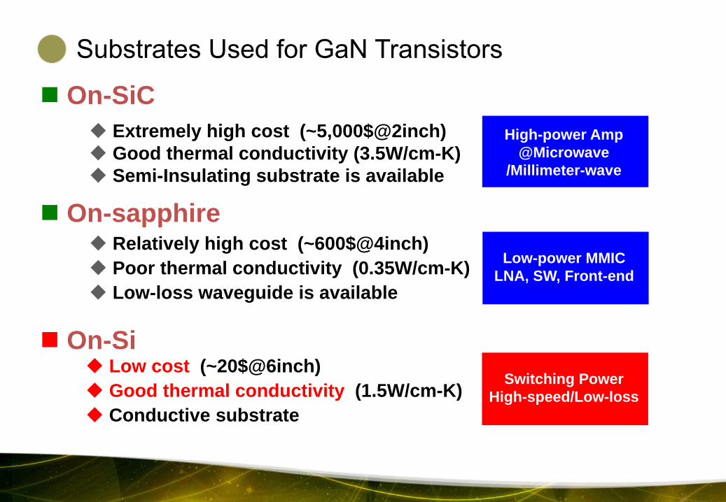
Substrates Used for GaN Transistors
On-sapphire
On-SiC
Relatively high cost (~600$@4inch) Poor thermal conductivity (0.35W/cm-K) Low-loss waveguide is available
On-Si
Extremely high cost (~5,000$@2inch) Good thermal conductivity (3.5W/cm-K) Semi-Insulating substrate is available
Low cost (~20$@6inch) Good thermal conductivity (1.5W/cm-K) Conductive substrate
Low-power MMICLNA, SW, Front-end
High-power Amp@Microwave
/Millimeter-wave
Switching PowerHigh-speed/Low-loss

GaN Epitaxial Growth Technique on Si Substrate
AlNAlGaN
Super-lattice Buffer
AlNGaN
CompressiveStrain
StrainRelaxation
GaN
Si(111) substrate
Lattice constant: Si>GaN>AlNThermal expansion coefficient: Si<GaN<AlN
MOCVD epitaxial structure
AlGaN/AlN initial layer GaN/AlN Super-lattice
6-inch epitaxy on Si
Mirror surface / Crack-free High mobility with good uniformity

Approaches for Normally-Off AlGaN/GaN HFETa-face FET (1) F-doped Gate (2) MIS-HFET (3) p-type Gate HFET
(GIT) (4)
Structure
Advantages Simple process Simple structure
Low leak current Controllability of
Vth
Low leak current Large Imax
Controllability of Vth
Good reliability confirmed
Challenges
Epitaxial Growth No polarization
induced charge Increase Imax
Stability of Doped Fluorine
Controllability of Vth
Stability of insulator/semiconductor interface
(3) S.Sugiura et al Phys Stat Solidi 5(2008) 1923.T.Imada et al Proc of IPEC 23C(2010),1027
(4)Y.Uemoto et al IEEE Trans Electron Dev, 54(2007) 3393.
(1) M.Kuroda et al IEEE Trans Electron Device,57(2010) 368.(2)Y.Cai et al IEEE Electron Dev Lett, 26(2005) 435.
Substrate
GaN
AlGaNS DG
Substrate
GaN
AlGaNS D
GInsulator
Substrate
GaN
AlGaNS DG
F-plasma treatment
Substrate
GaN
AlGaNS D
G
P-AlGaN
(e.g. a-GaN/r-sapphire)

Gate Injection Transistor (GIT)
Normally-Off Operationp-AlGaN lifts up the potentialat the channel
Low on-resistanceHole injection from p-AlGaN to AlGaN/GaN channelincreases the drain current using conductivity modulation
Gate
p-AlGaNi-AlGaN
i-GaN
Source Drain
mh << me
Schematic cross-section A New Normally-Off GaN Transistor - GIT -
I-V characteristics
Normally off
PanasonicGITNormally on
Conventional GaN-FET
Large drain current
0.0
0.2
0.4
0.6
0.8
1.0
-4 -2 0 2 4 6Gate Voltage (V)
Dra
in C
urre
nt(a
.u.)

GIT Operation
p‐AlGaNi‐AlGaN
i‐GaN
GateSourceDrain
- - --
No current flows
- - ---
off
p‐AlGaNi‐AlGaN
i-GaN
- - - - - - - - - -
GateSourceDrain
mh<< me
- - -
Large drain current
-- -- -- -- -
++
+ + +-
on
Vg = 0V p-gate potential depletes the
channel under the gate↓
No drain current
Vg > Vf of GaN-PN junctionHole injection
↓Electron generation
↓Large drain current
(conductivity modulation)

Reverse I-V Characteristics
No voltage-offset at the Vgs of 5V (FET mode) GIT can be operated as if a diode at the Vgs of 0V
(Reverse-conduction mode)
-400
-300
-200
-100
0
100
200
300
400
-10 -8 -6 -4 -2 0 2 4 6 8 10
Vds (V)
()
Vgs=5V
4V
3V
2V
1V, 0Vstep=+1V
FET mode
ReverseConduction
Mode
Vds (V)
Ids
(mA
/mm
)
Vgs=0V
Vgs=5V
On-state I-V Characteristics
Vgs=5V

Current-Collapse-FreeNo destruction and degradation was not observed up to 600V.
0
2
4
6
8
10
300 400 500 600 700
Drain-Source Voltage (V)
On-
resi
stan
ce (a
.u.)
Measured under the condition of practical use
Low On-Resistance
High FrequencyOperation
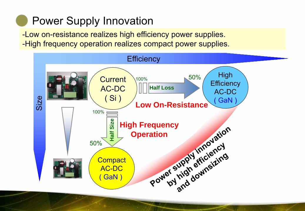
-Low on-resistance realizes high efficiency power supplies.-High frequency operation realizes compact power supplies.-Low on-resistance realizes high efficiency power supplies.-High frequency operation realizes compact power supplies.
CurrentAC-DC( Si )
HighEfficiencyAC-DC( GaN )
CompactAC-DC( GaN )
Half Loss
Hal
f Siz
e
Efficiency
Siz
e
100% 50%
100%
50%
Power Supply Innovation

Conclusion
GaN Predominance- Normally-Off- Current-Collapse-Free- Zero Recovery
Applications- Power Supply for
Data Centers and Base Transceiver Stations- Automotive (HEV / EV / PHEV) etc.

Request for your special attention and precautions in using the technical information andsemiconductors described in this book
(1) If any of the products or technical information described in this book is to be exported or provided to non-residents, the laws and regulations of the exporting country, especially, those with regard to security export control, must be observed.
(2) The technical information described in this book is intended only to show the main characteristics and application circuit examples of the products. No license is granted in and to any intellectual property right or other right owned by Panasonic Corporation or any other company. Therefore, no responsibility is assumed by our company as to the infringement upon any such right owned by any other company which may arise as a result of the use of technical information described in this book.
(3) The products described in this book are intended to be used for general applications (such as office equipment, communications equipment, measuring instruments and household appliances), or for specific applications as expressly stated in this book.Consult our sales staff in advance for information on the following applications:� Special applications (such as for airplanes, aerospace, automotive equipment, traffic signaling equipment, combustion equipment,
life support systems and safety devices) in which exceptional quality and reliability are required, or if the failure or malfunction of the products may directly jeopardize life or harm the human body.
It is to be understood that our company shall not be held responsible for any damage incurred as a result of or in connection with your using the products described in this book for any special application, unless our company agrees to your using the products in this book for any special application.
(4) The products and product specifications described in this book are subject to change without notice for modification and/or im-provement. At the final stage of your design, purchasing, or use of the products, therefore, ask for the most up-to-date Product Standards in advance to make sure that the latest specifications satisfy your requirements.
(5) When designing your equipment, comply with the range of absolute maximum rating and the guaranteed operating conditions (operating power supply voltage and operating environment etc.). Especially, please be careful not to exceed the range of absolute maximum rating on the transient state, such as power-on, power-off and mode-switching. Otherwise, we will not be liable for any defect which may arise later in your equipment.
Even when the products are used within the guaranteed values, take into the consideration of incidence of break down and failure mode, possible to occur to semiconductor products. Measures on the systems such as redundant design, arresting the spread of fire or preventing glitch are recommended in order to prevent physical injury, fire, social damages, for example, by using the products.
(6) Comply with the instructions for use in order to prevent breakdown and characteristics change due to external factors (ESD, EOS, thermal stress and mechanical stress) at the time of handling, mounting or at customer's process. When using products for which damp-proof packing is required, satisfy the conditions, such as shelf life and the elapsed time since first opening the packages.
(7) This book may be not reprinted or reproduced whether wholly or partially, without the prior written permission of our company.
20100202