Embed Size (px)
Citation preview
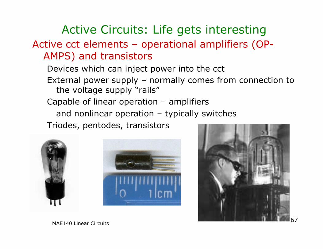
MAE140 Linear Circuits 67
Active Circuits: Life gets interesting Active cct elements – operational amplifiers (OP-
AMPS) and transistors Devices which can inject power into the cct External power supply – normally comes from connection to
the voltage supply “rails” Capable of linear operation – amplifiers
and nonlinear operation – typically switches Triodes, pentodes, transistors
MAE140 Linear Circuits 68
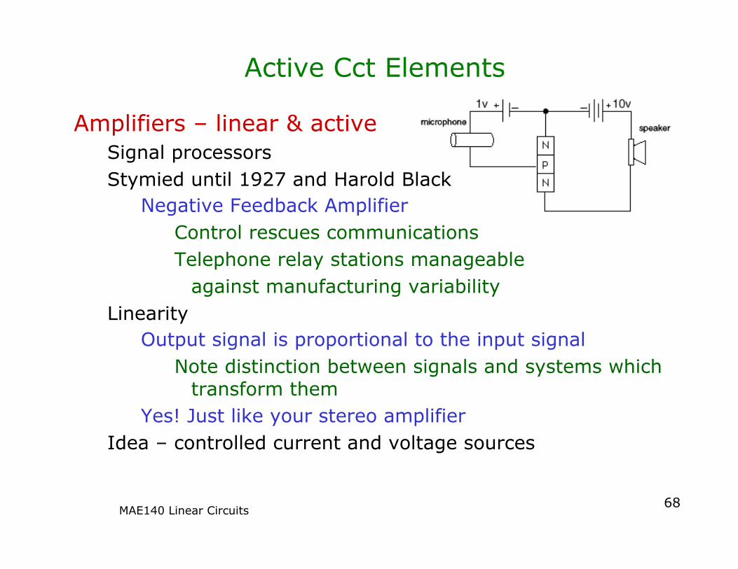
Active Cct Elements
Amplifiers – linear & active Signal processors Stymied until 1927 and Harold Black
Negative Feedback Amplifier Control rescues communications Telephone relay stations manageable against manufacturing variability
Linearity Output signal is proportional to the input signal
Note distinction between signals and systems which transform them
Yes! Just like your stereo amplifier Idea – controlled current and voltage sources
MAE140 Linear Circuits 69
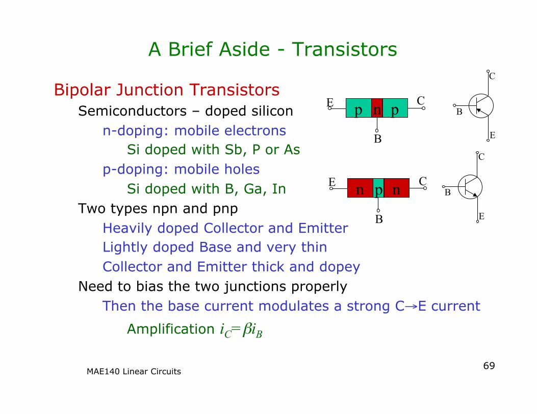
A Brief Aside - Transistors
Bipolar Junction Transistors Semiconductors – doped silicon
n-doping: mobile electrons Si doped with Sb, P or As
p-doping: mobile holes Si doped with B, Ga, In
Two types npn and pnp Heavily doped Collector and Emitter Lightly doped Base and very thin Collector and Emitter thick and dopey
Need to bias the two junctions properly Then the base current modulates a strong C→E current
Amplification iC=βiB
B
E
C
B
E
C
n p n E
B
C
p n p E
B
C
MAE140 Linear Circuits 70
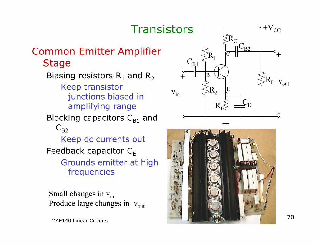
Transistors
Common Emitter Amplifier Stage Biasing resistors R1 and R2
Keep transistor junctions biased in amplifying range
Blocking capacitors CB1 and CB2 Keep dc currents out
Feedback capacitor CE Grounds emitter at high
frequencies
B
E
C
+VCC
RL
RE
RC
R2
R1 CB1
CB2
CE vin
vout +
-
+
-
Small changes in vin Produce large changes in vout
MAE140 Linear Circuits 71
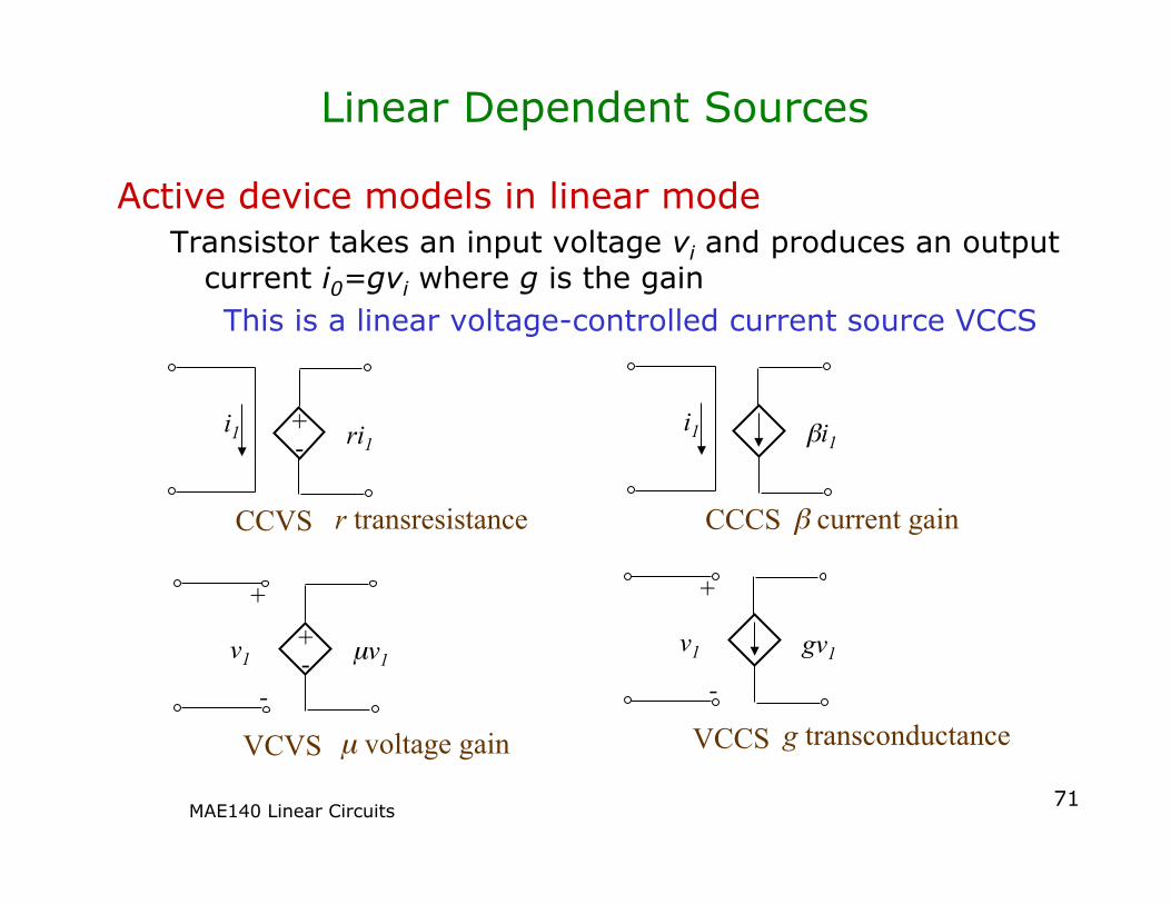
Linear Dependent Sources
Active device models in linear mode Transistor takes an input voltage vi and produces an output
current i0=gvi where g is the gain This is a linear voltage-controlled current source VCCS
+ -
i1 ri1
CCVS
i1 βi1
CCCS
VCVS
+ - v1 µv1
+
- VCCS
v1 gv1
+
-
r transresistance
g transconductance
β current gain
µ voltage gain
MAE140 Linear Circuits 72
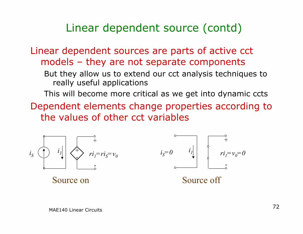
Linear dependent source (contd)
Linear dependent sources are parts of active cct models – they are not separate components But they allow us to extend our cct analysis techniques to
really useful applications This will become more critical as we get into dynamic ccts
Dependent elements change properties according to the values of other cct variables
+ -
i1 ri1=riS=v0 iS
+
-
i1 ri1=v0=0 iS=0
+
-
Source on Source off
MAE140 Linear Circuits 73
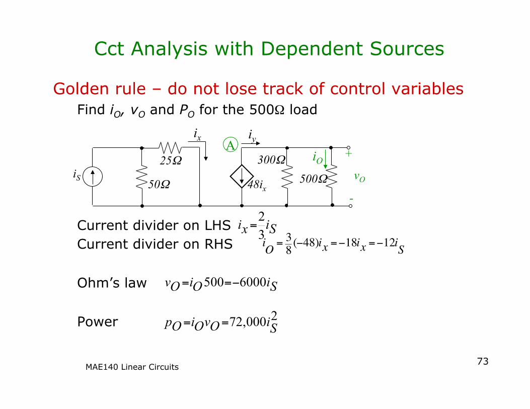
Cct Analysis with Dependent Sources
Golden rule – do not lose track of control variables Find iO, vO and PO for the 500Ω load
Current divider on LHS Current divider on RHS
Ohm’s law
Power
iy ix
iO iS 48ix
500Ω vO 300Ω 25Ω
50Ω
+
-
A
Sixi 32
=
€
iO = 38(−48)ix =−18ix =−12iS
SiOiOv 6000500 −==
2000,72 SiOvOiOp ==
MAE140 Linear Circuits 74
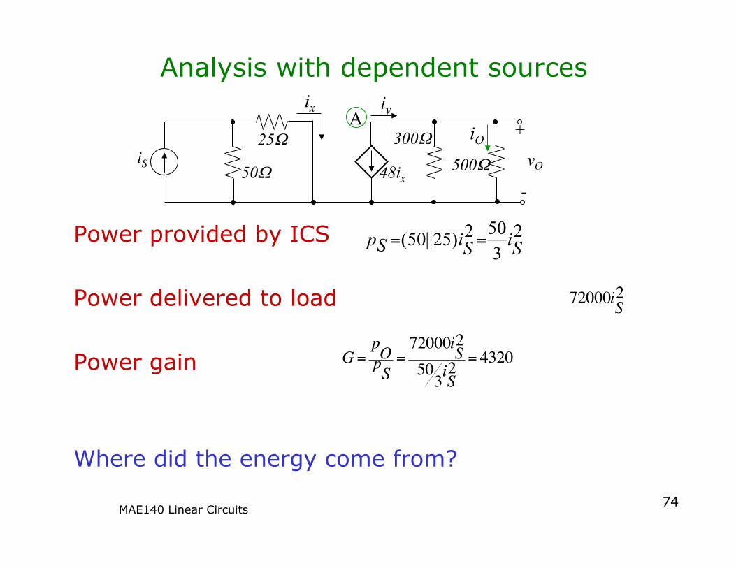
Analysis with dependent sources
Power provided by ICS
Power delivered to load
Power gain
Where did the energy come from?
iy ix
iO iS 48ix
500Ω vO 300Ω 25Ω
50Ω
+
-
A
23502)25||50( SiSiSp ==
€
72000iS2
€
G =pOpS
=72000iS
2
503iS2 = 4320
MAE140 Linear Circuits 75
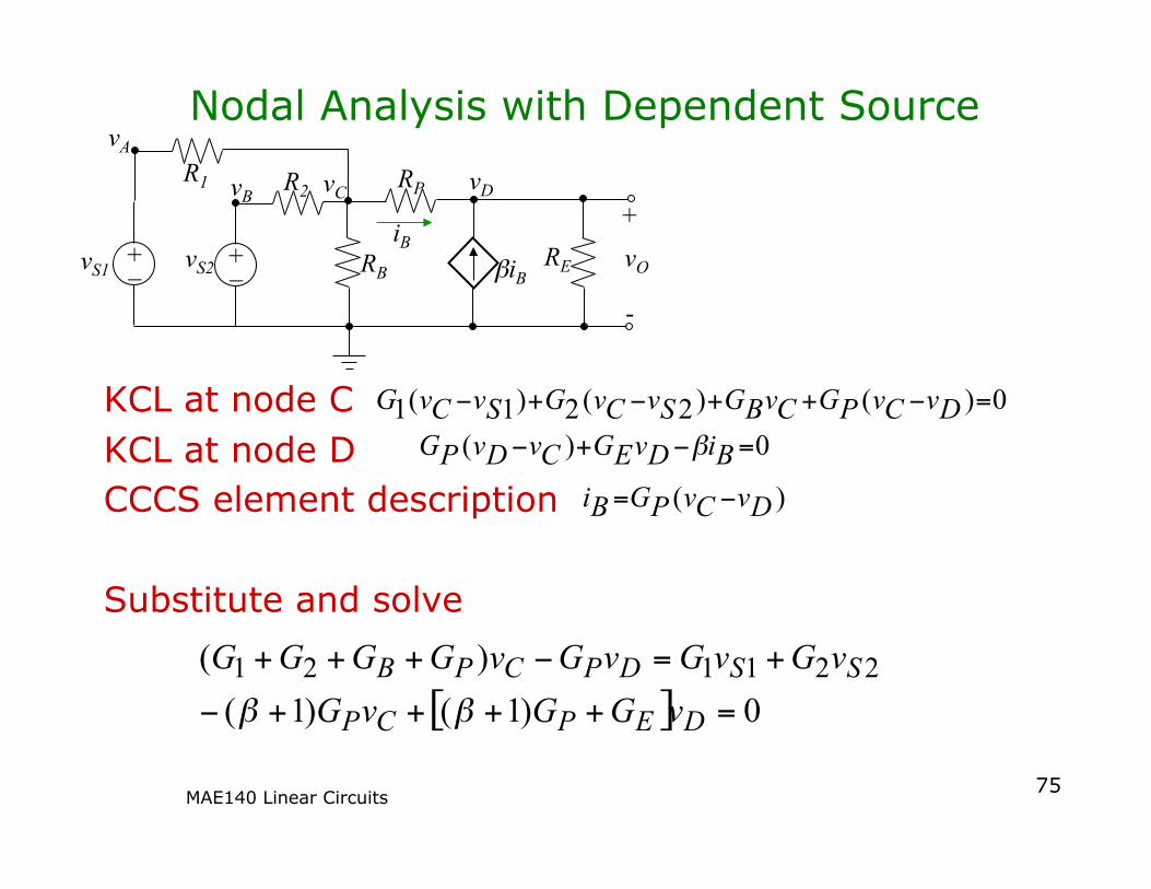
Nodal Analysis with Dependent Source
KCL at node C KCL at node D CCCS element description
Substitute and solve
+ _ vS1 + _ vS2
R1 R2
RB
RP
RE iB
βiB
vD vC vB
vA
vO +
-
0)()2(2)1(1 =−++−+− DvCvPGCvBGSvCvGSvCvG0)( =−+− BiDvEGCvDvPG β
)( DvCvPGBi −=
[ ] 0)1()1()( 221121
=++++−
+=−+++
DEPCP
SSDPCPBvGGvG
vGvGvGvGGGGββ
MAE140 Linear Circuits 76
T&R, 5th ed, Example 4-3 p 148
+ _ + - +
vx µvx
R1
vO vS R2
R3
R4
+
- -
iO Find vO in terms of vS What happens as µ→∞?
+ - +
vx µvx
R1 vO R2
R3
R4
+
- -
iO
1RSv
vA vB Node A:
Node B:
Solution:
SvGBvGAvGGG 13)321( =−++
AvxvBv µµ −=−=
SvGGGG
AvBvOv
+++
−=−==
3)1(211µ
µµ
For large gains µ: (1+µ)G3>>G1+G2
SvRR
SvGG
Ov13
3)1(1 −≈
+
−≈
µ
µ
This is a model of an inverting op-amp
MAE140 Linear Circuits 77
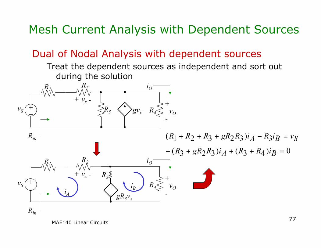
Mesh Current Analysis with Dependent Sources
Dual of Nodal Analysis with dependent sources Treat the dependent sources as independent and sort out
during the solution
+ _
R1 R2
R3 R4 vS vx
vO + +
-
-
Rin
iO
gvx
+ -
+ _
R1 R2
R3 R4 vS
vx vO
+ +
-
-
Rin
iO
gR3vx iA
iB
0)43()323(3)32321(
=+++−
=−+++
BiRRAiRgRR
vBiRAiRgRRRR S
MAE140 Linear Circuits 78
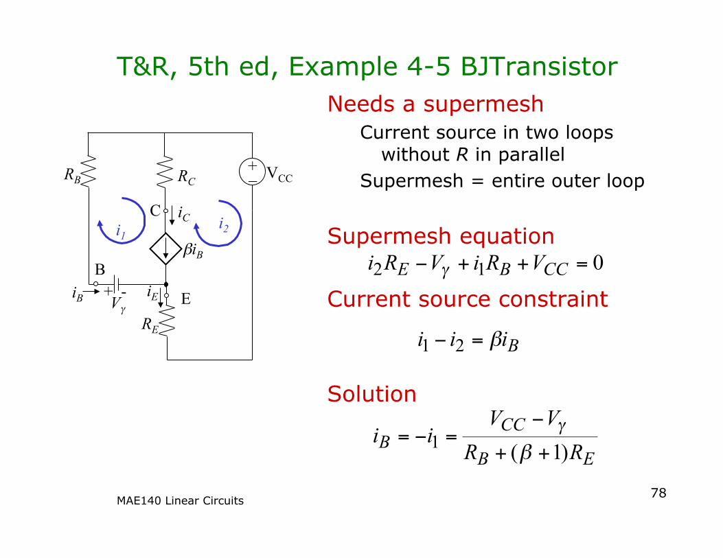
T&R, 5th ed, Example 4-5 BJTransistor Needs a supermesh
Current source in two loops without R in parallel
Supermesh = entire outer loop
Supermesh equation
Current source constraint
Solution
+ _ RB RC
RE
B
C
E Vγ + -
VCC
iB
iC
iE
βiB i1
i2
012 =++− CCBE VRiVRi γ
Biii β=− 21
EB
CCB RR
VVii
)1(1 ++
−=−=
βγ
MAE140 Linear Circuits 79
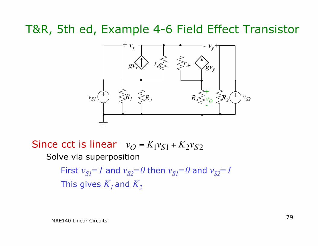
T&R, 5th ed, Example 4-6 Field Effect Transistor
Since cct is linear Solve via superposition
First vS1=1 and vS2=0 then vS1=0 and vS2=1 This gives K1 and K2
+ _ R1 + _ R2 R3 R4 vS1 vS2
vx
gvx
vy
gvy rds rds
+ + - -
-
+ vO
2211 SSO vKvKv +=
MAE140 Linear Circuits 80
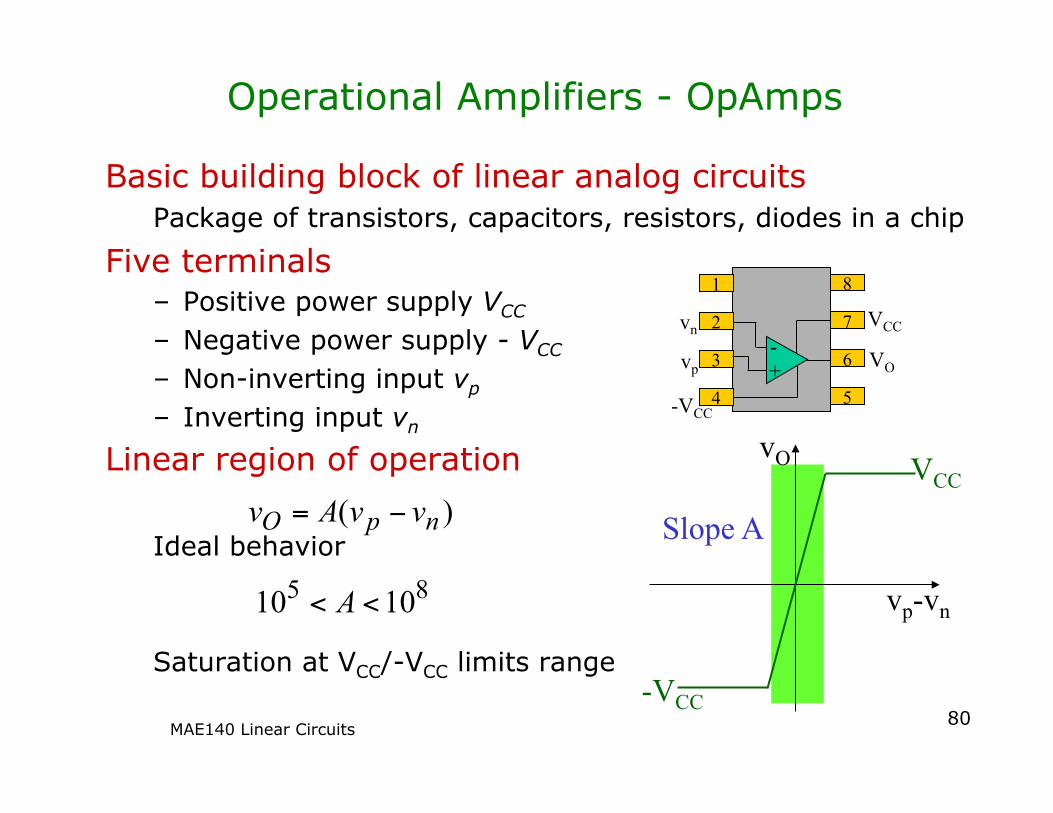
Operational Amplifiers - OpAmps
Basic building block of linear analog circuits Package of transistors, capacitors, resistors, diodes in a chip
Five terminals – Positive power supply VCC – Negative power supply - VCC – Non-inverting input vp – Inverting input vn
Linear region of operation
Ideal behavior
Saturation at VCC/-VCC limits range
1
2
3
4
8
7
6
5 + -
VCC
-VCC
vn
vp VO
vO VCC
-VCC
vp-vn
Slope A )( npO vvAv −=
85 1010 << A
MAE140 Linear Circuits 81
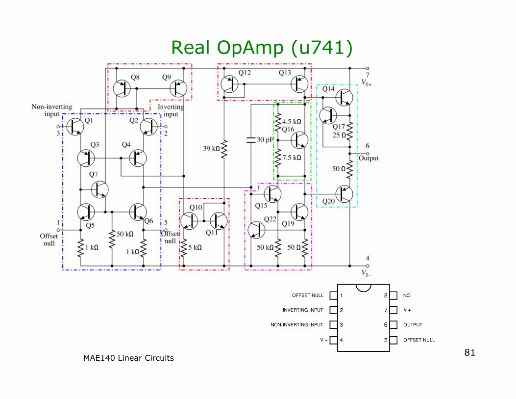
Real OpAmp (u741)
MAE140 Linear Circuits 82
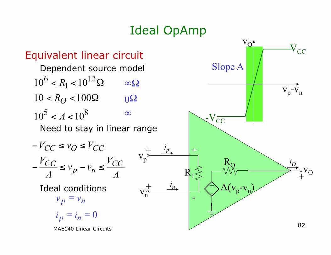
Ideal OpAmp
Equivalent linear circuit Dependent source model
Need to stay in linear range
Ideal conditions
vO VCC
-VCC
vp-vn
Slope A
+ -
R1 RO
A(vp-vn)
+
-
ip
in
iO vO
vn
vp
+
+
+
85
121
6
1010
100101010
<<
Ω<<
Ω<<
A
RR
O∞ Ω Ω ∞
0
AVvv
AV
VvV
CCnp
CC
CCOCC
≤−≤−
≤≤−
0 = =
=
n p
n p i i
v v
MAE140 Linear Circuits 83
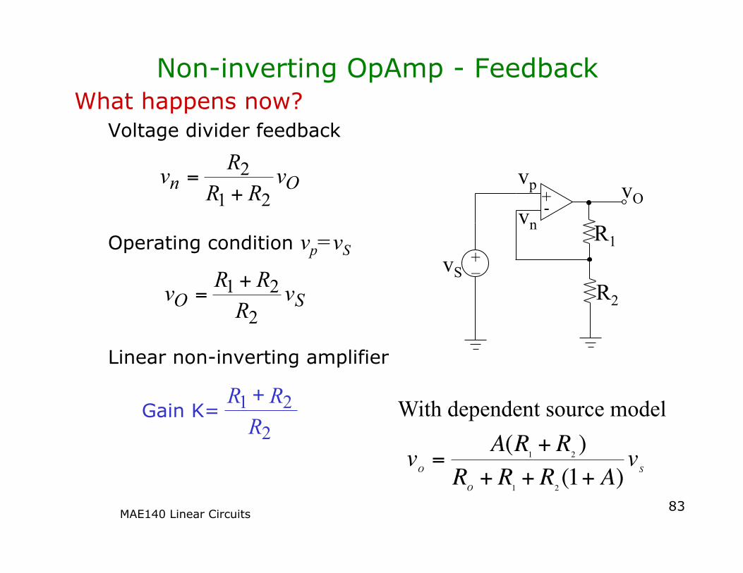
Non-inverting OpAmp - Feedback What happens now?
Voltage divider feedback
Operating condition vp=vS
Linear non-inverting amplifier
Gain K=
+ -
+ _
vp
vS
vO
R2
R1 vn
On vRR
Rv21
2+
=
SO vRRRv2
21 +=
2 2 1
R R R +
€
vO
=A(R
1+ R
2)
RO
+ R1+ R
2(1+ A)
vS
With dependent source model
MAE140 Linear Circuits 84
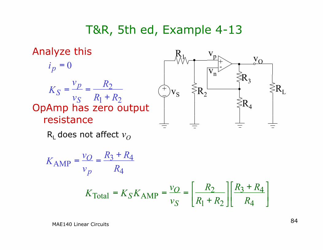
T&R, 5th ed, Example 4-13
Analyze this
OpAmp has zero output resistance RL does not affect vO
+ -
+ _
vp
vS
vO
R4
R3 vn
RL
R1
R2 2 1
2
0
R R R
v v
K
i
S p
S
p
+ = =
=
4 4 3
AMP R R R
v v K
p O + = =
+
+ = = =
4 4 3
2 1 2
AMP Total R R R
R R R
v v K K K
S O
S
MAE140 Linear Circuits 85
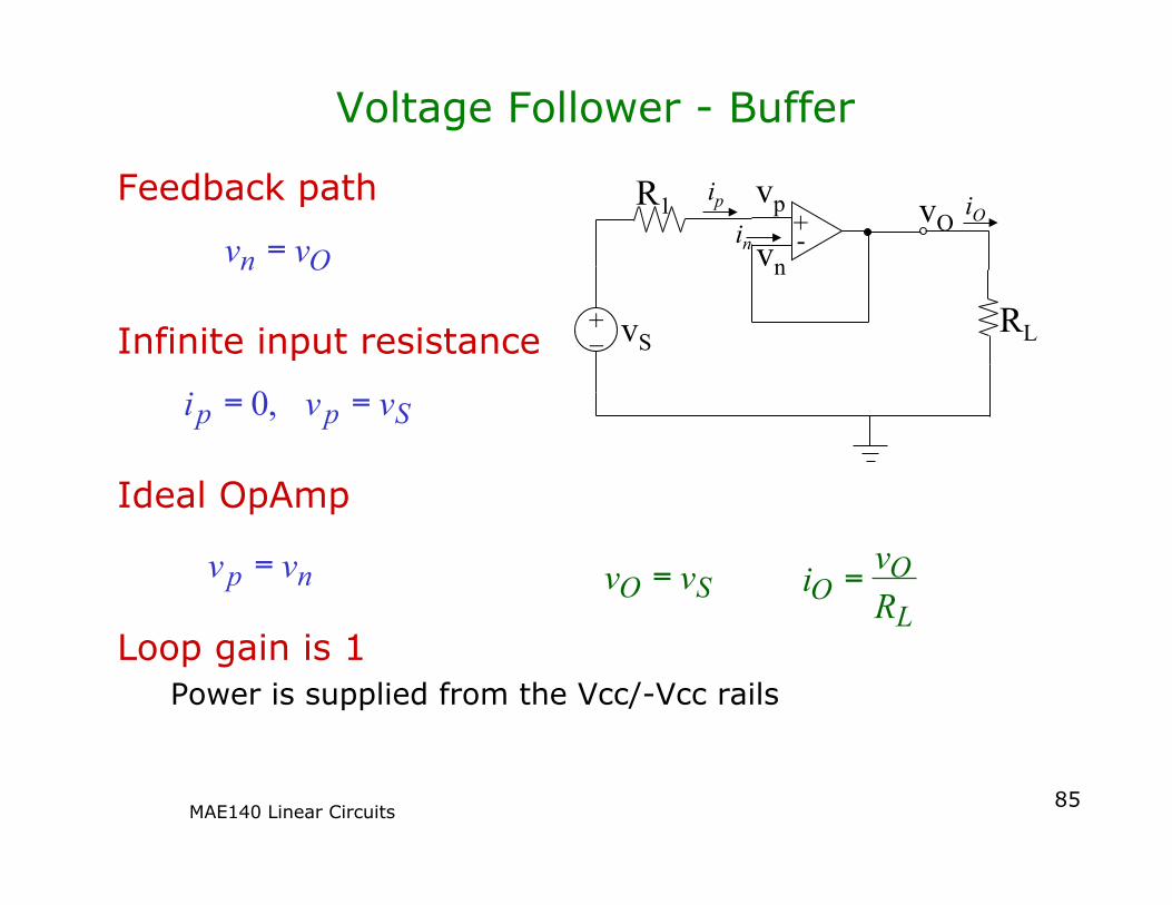
Voltage Follower - Buffer
Feedback path
Infinite input resistance
Ideal OpAmp
Loop gain is 1 Power is supplied from the Vcc/-Vcc rails
+ -
+ _
vp
vS
vO vn
RL
R1 iO in
ip
O n v v =
S p p v v i = = , 0
n p v v = S O v v =
L O
O R v i =
MAE140 Linear Circuits 86
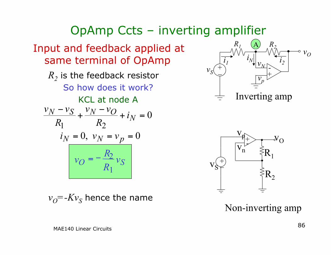
OpAmp Ccts – inverting amplifier Input and feedback applied at
same terminal of OpAmp R2 is the feedback resistor
So how does it work? KCL at node A
vO=-KvS hence the name
+ _ + - i1
R1 R2
i2 iN
vp
vN vS
vO A
+ -
+ _
vp
vS
vO
R2
R1 vn
021
=+−
+−
NONSN i
Rvv
Rvv
0,0 === pNN vvi
S O v R R v
1 2 - =
Inverting amp
Non-inverting amp
MAE140 Linear Circuits 87
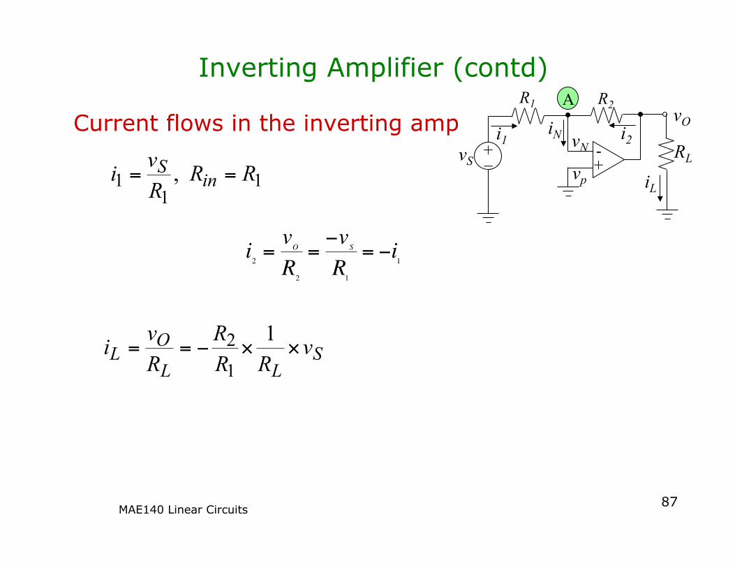
Inverting Amplifier (contd)
Current flows in the inverting amp + _ + - i1
R1 R2
i2 iN
vp
vN vS
vO A
11
1 , RRRvi inS ==
€
i2=v
O
R2
=−v
S
R1
= −i1
iL RL
SLL
OL v
RRR
Rvi ××−==
11
2
MAE140 Linear Circuits 88
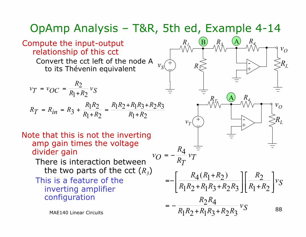
OpAmp Analysis – T&R, 5th ed, Example 4-14 Compute the input-output
relationship of this cct Convert the cct left of the node A
to its Thévenin equivalent
+ _ + -
R4 vO
A
RL vT
RT
21323121
2121
3
212
RRRRRRRR
RRRR
RinRTR
SvRRR
OCvTv
+++
=+
+==
+==
SvRRRRRRRR
SvRRR
RRRRRRRRR
TvTRR
Ov
32312142
212
323121
)21(4
4
++−=
+++
+−=
−=
+ _ + -
R1 R4
vS
vO A
RL
B
R2
R3
Note that this is not the inverting amp gain times the voltage divider gain There is interaction between
the two parts of the cct (R3) This is a feature of the
inverting amplifier configuration
MAE140 Linear Circuits 89
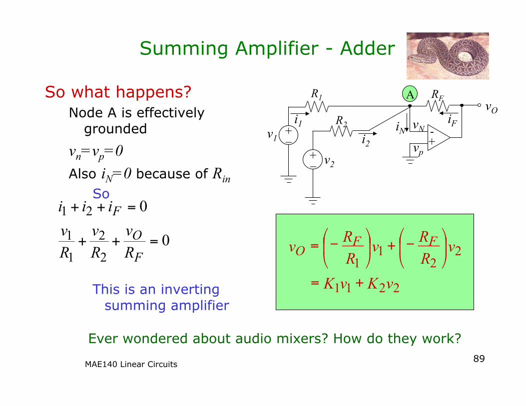
Summing Amplifier - Adder
So what happens? Node A is effectively
grounded
vn=vp=0 Also iN=0 because of Rin
So
This is an inverting summing amplifier
+ _ + - i1
R1 RF
iF iN vp
vN v1
vO A
+ _
i2 R2
v2
0
0
2
2
1
1
21
=++
=++
F
O
F
Rv
Rv
Rv
iii
2 2 1 1
2 2
1 1
v K v K
v R R v
R R v F F
O
+ =
- +
- =
Ever wondered about audio mixers? How do they work?
MAE140 Linear Circuits 90
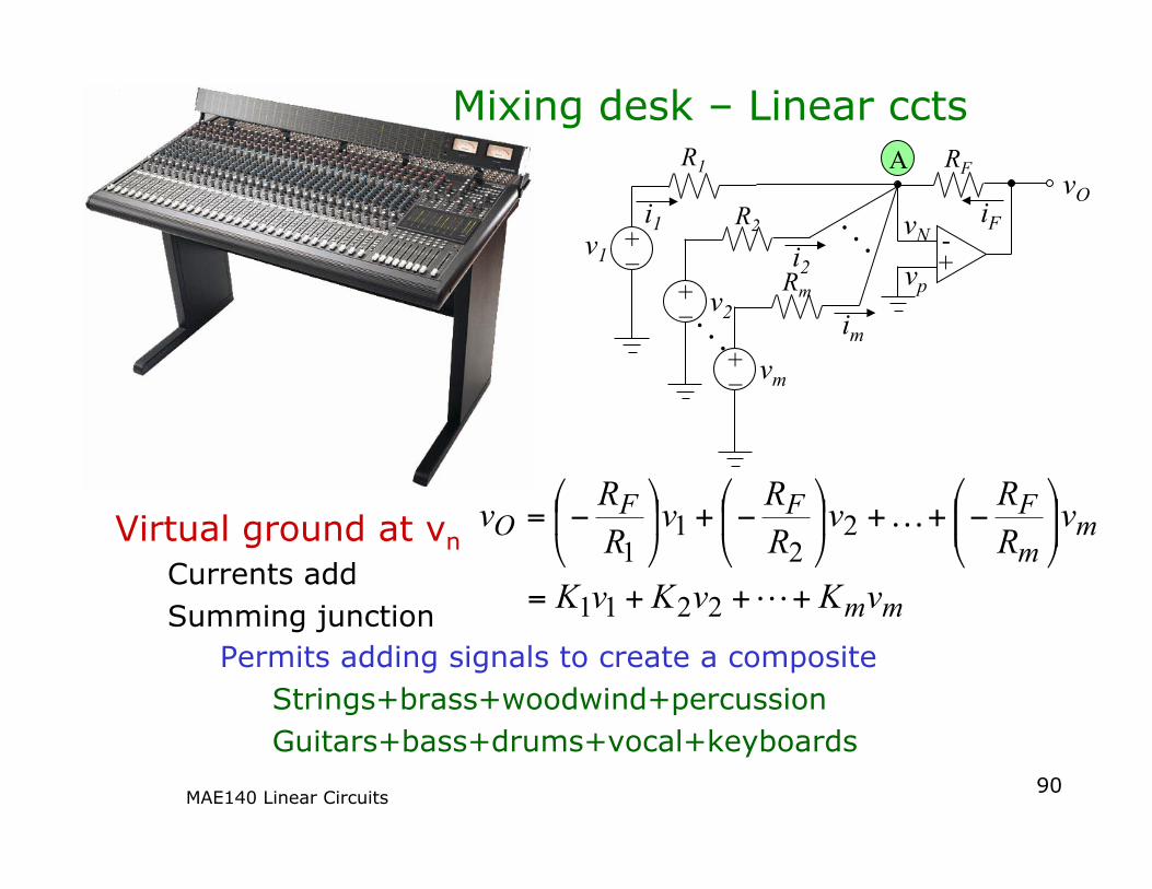
Virtual ground at vn Currents add Summing junction
Permits adding signals to create a composite Strings+brass+woodwind+percussion Guitars+bass+drums+vocal+keyboards
mm
mmFFF
O
vKvKvK
vRRv
RRv
RRv
+++=
−++
−+
−=
…
2211
22
11
+ _ + - i1
R1 RF
iF
vp
vN v1
vO A
+ _
i2 R2
v2
+ _
im vm
Rm
Mixing desk – Linear ccts
MAE140 Linear Circuits 91
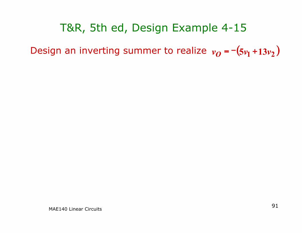
T&R, 5th ed, Design Example 4-15
Design an inverting summer to realize ( ) 2 1 13 5 v v v O + - =
MAE140 Linear Circuits 92
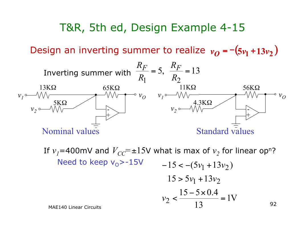
T&R, 5th ed, Design Example 4-15
Design an inverting summer to realize
Inverting summer with
If v1=400mV and VCC=±15V what is max of v2 for linear opn? Need to keep vO>-15V
( ) 2 1 13 5 v v v O + - =
13,521==
RR
RR FF
+ -
13KΩ 65KΩ v1 vO
5KΩ v2
11KΩ
+ -
56KΩ v1 vO
4.3KΩ v2
Nominal values Standard values
V113
4.051513515
)135(15
2
21
21
=×−
<
+>
+−<−
v
vvvv
MAE140 Linear Circuits 93
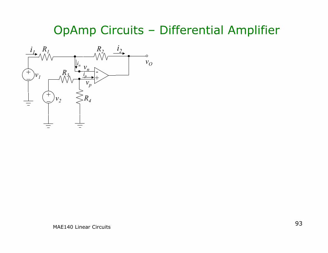
OpAmp Circuits – Differential Amplifier i1 R1
v1 + - + _
+ _ v2
vn
vp
vO R3
R4
R2
ip
i2
in
MAE140 Linear Circuits 94
OpAmp Circuits – Differential Amplifier
Use superposition to analyze v2=0: inverting amplifier
v1=0: non-inverting amplifier plus voltage divider
K1 inverting gain K2 non-inverting gain
11
21 v
RRvO −=
21
21
43
42 v
RRR
RRRvO
+
+=
i1 R1
v1 + - + _
+ _ v2
vn
vp
vO R3
R4
R2
ip
i2
in
2 2 1 1
2 1
2 1 4 3
4 1 2
2 1
v K v K
v R
R R R R
R v R R
v v v O O O
+ - =
+
+
+
- =
+ =
1
MAE140 Linear Circuits 95
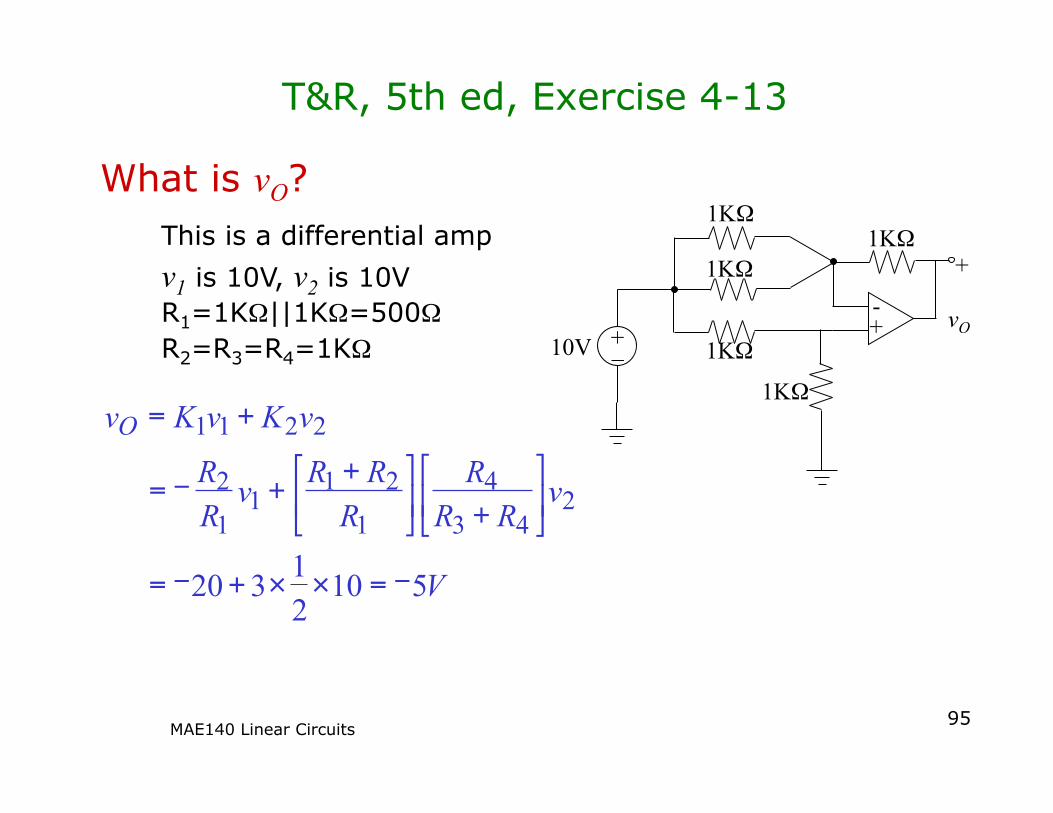
T&R, 5th ed, Exercise 4-13
What is vO?
+ _
1KΩ
10V
+ -
1KΩ
1KΩ
1KΩ
1KΩ
vO
+
V
v R R
R R
R R v R R
v K v K v O
5 10 2 1 3 20
2 4 3
4 1
2 1 1
1 2
2 2 1 1
- = × × + - =
+
+
+ - =
+ =
This is a differential amp v1 is 10V, v2 is 10V R1=1KΩ||1KΩ=500Ω R2=R3=R4=1KΩ
MAE140 Linear Circuits 96
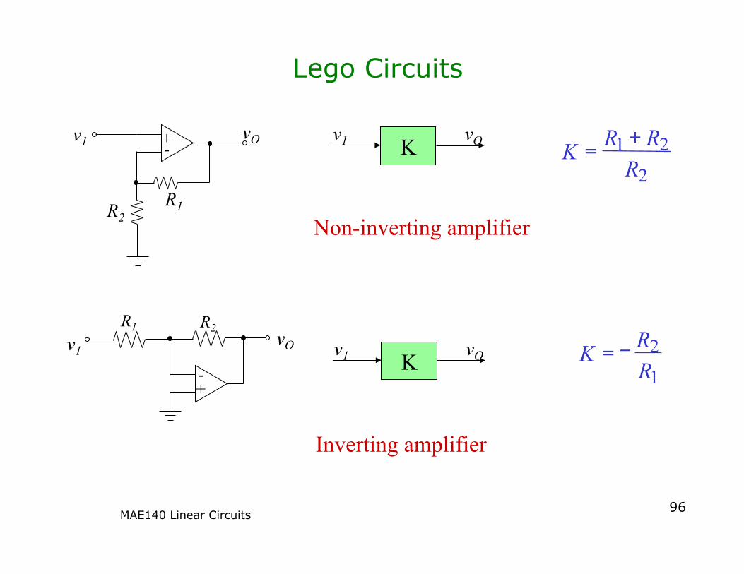
Lego Circuits
+ -
v1 vO
R2 R1
+ -
R1 R2 v1 vO
K v1 vO
K v1 vO
2 2 1
R R R K
+ =
1 2
R R K - =
Non-inverting amplifier
Inverting amplifier
MAE140 Linear Circuits 97
Lego Circuits (contd)
+ -
R1
R2
v1 vO
v2
RF K1
K2 +
v1
vO
v2
2 2
1 1
R R K
R R K
F
F
- =
- =
R1 v1 + -
v2
vO R3
R4
R2
K1
K2 +
v1
vO
v2
+
+
=
- =
4 3 4
1 2 1
2
1 2
1
R R R
R R R K
R R K
Inverting summer
Differential amplifier
MAE140 Linear Circuits 98
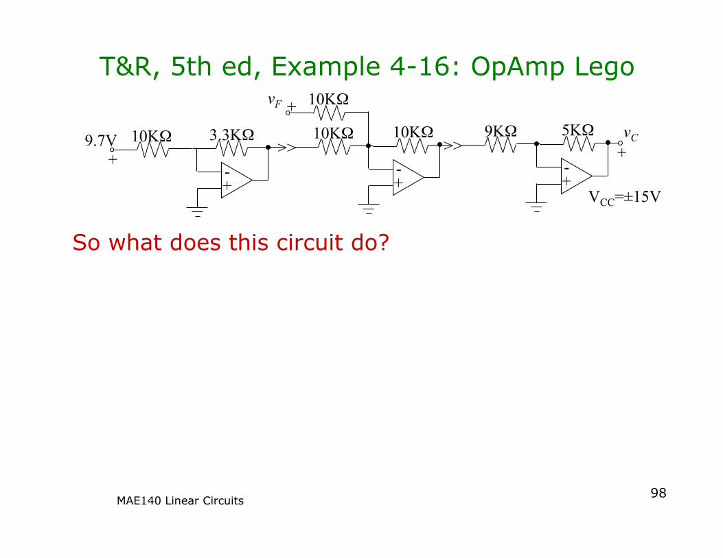
T&R, 5th ed, Example 4-16: OpAmp Lego
So what does this circuit do?
10KΩ 9.7V
+ - + - + -
3.3KΩ 10KΩ 10KΩ 9KΩ 5KΩ >> >>
10KΩ vF
+ + vC
+
VCC=±15V
MAE140 Linear Circuits 99
Example 4-16: OpAmp Lego
So what does this circuit do?
It converts tens of ºF to tens of ºC Max current drawn by each stage is 1.5mA
10KΩ 9.7V
+ - + - + -
3.3KΩ 10KΩ 10KΩ 9KΩ 5KΩ >> >>
10KΩ vF
+ + vC
+
VCC=±15V
-0.33 -1
-1
+ 95−
9.7V -3.2V
vF
3.2-vF
vC
MAE140 Linear Circuits 100
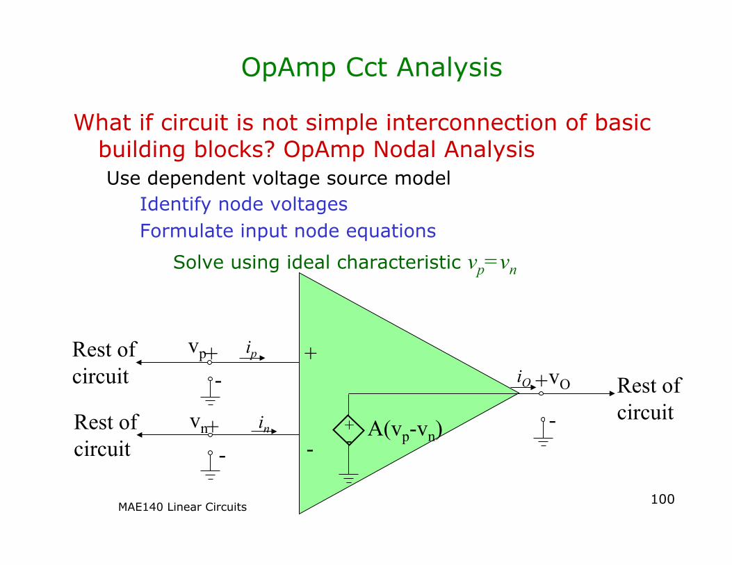
OpAmp Cct Analysis
What if circuit is not simple interconnection of basic building blocks? OpAmp Nodal Analysis Use dependent voltage source model
Identify node voltages Formulate input node equations
Solve using ideal characteristic vp=vn
+ - A(vp-vn)
+
-
ip
in
iO vO
vn
vp +
+
+
-
- -
Rest of circuit
Rest of circuit
Rest of circuit
MAE140 Linear Circuits 101
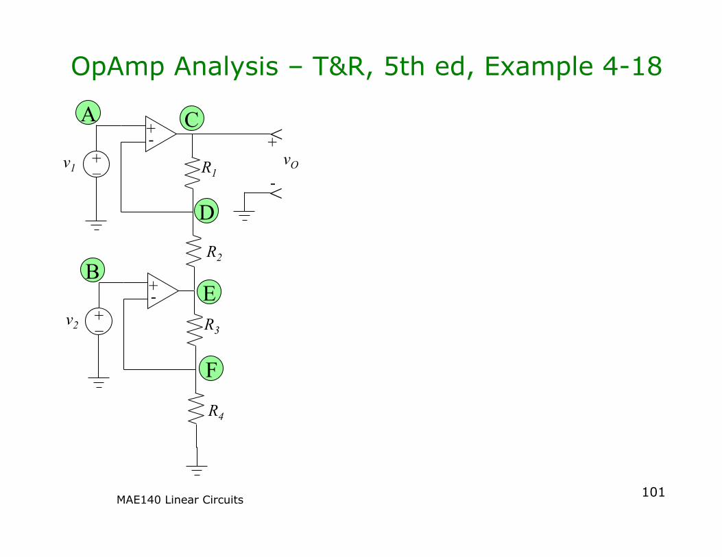
OpAmp Analysis – T&R, 5th ed, Example 4-18
R1 v1
+ - + _
R3 v2
+ - + _
R2
R4
<
<
vO -
+ A
B
C
D
E
F
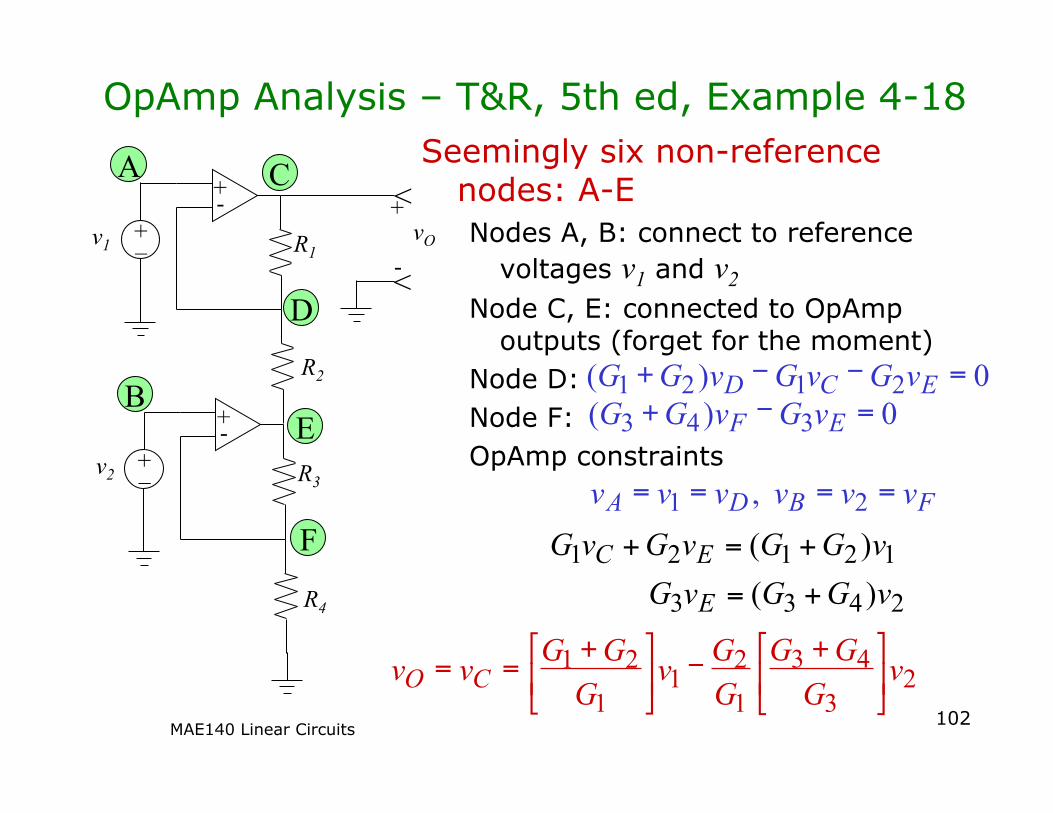
MAE140 Linear Circuits 102
OpAmp Analysis – T&R, 5th ed, Example 4-18 Seemingly six non-reference
nodes: A-E Nodes A, B: connect to reference
voltages v1 and v2 Node C, E: connected to OpAmp
outputs (forget for the moment) Node D: Node F: OpAmp constraints
R1 v1
+ - + _
R3 v2
+ - + _
R2
R4
<
<
vO -
+ A
B
C
D
E
F
0 ) ( 2 1 2 1 = - - + E C D v G v G v G G 0 ) ( 3 4 3 = - + E F v G v G G
F B D A v v v v v v = = = = 2 1 ,
2433
12121)()(vGGvGvGGvGvG
E
EC+=
+=+
2 3
4 3 1 2
1 1
2 1 v G
G G G G v
G G G v v C O
+
-
+
= =
MAE140 Linear Circuits 103
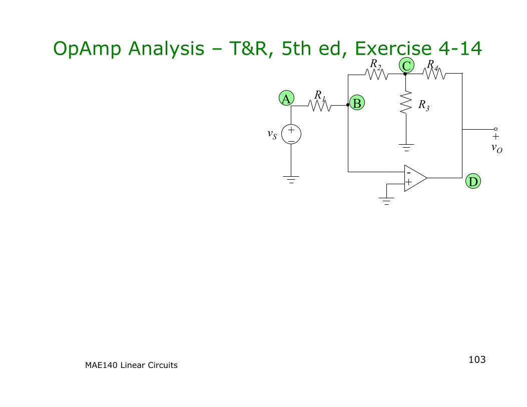
OpAmp Analysis – T&R, 5th ed, Exercise 4-14
+ _
R1
vS
+ -
R4 R2
R3
vO +
B A
C
D
MAE140 Linear Circuits 104
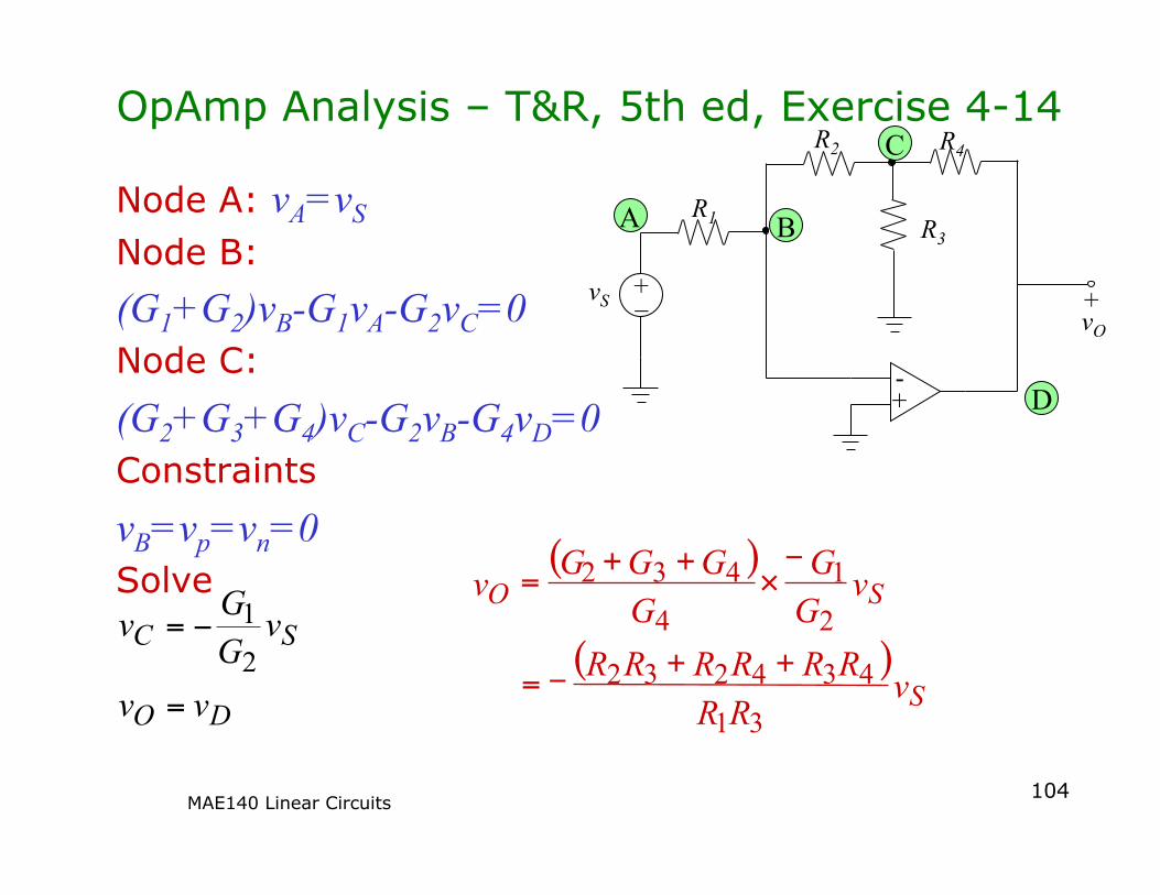
OpAmp Analysis – T&R, 5th ed, Exercise 4-14
Node A: vA=vS Node B: (G1+G2)vB-G1vA-G2vC=0 Node C:
(G2+G3+G4)vC-G2vB-G4vD=0 Constraints
vB=vp=vn=0 Solve
+ _
R1
vS
+ -
R4 R2
R3
vO +
B A
C
D
DO
SC
vv
vGGv
=
−=2
1
( )
( ) S
S O
v R R
R R R R R R
v G G
G G G G v
3 1 4 3 4 2 3 2
2 1
4 4 3 2
+ + - =
- × + +
=
MAE140 Linear Circuits 105
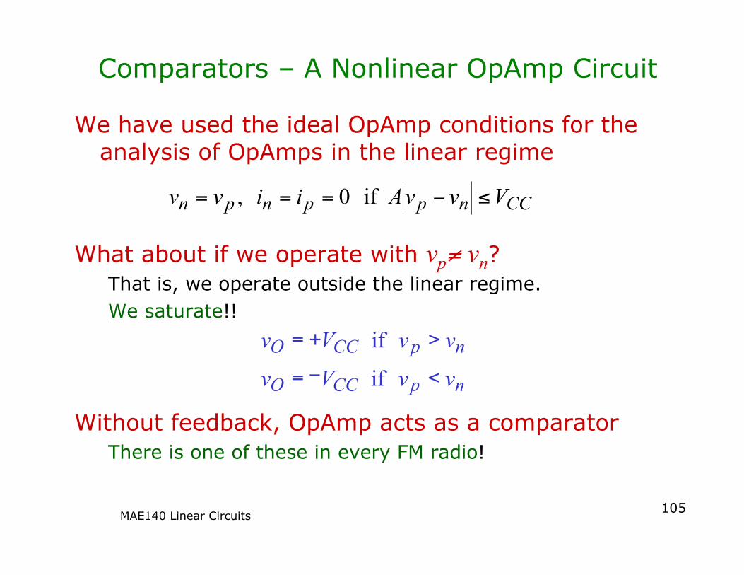
Comparators – A Nonlinear OpAmp Circuit
We have used the ideal OpAmp conditions for the analysis of OpAmps in the linear regime
What about if we operate with vp≠ vn? That is, we operate outside the linear regime. We saturate!!
Without feedback, OpAmp acts as a comparator There is one of these in every FM radio!
CCnppnpn VvvAiivv ≤−=== if0,
n p CC O
n p CC O v v V v
v v V v < - =
> + =
if
if
MAE140 Linear Circuits 106
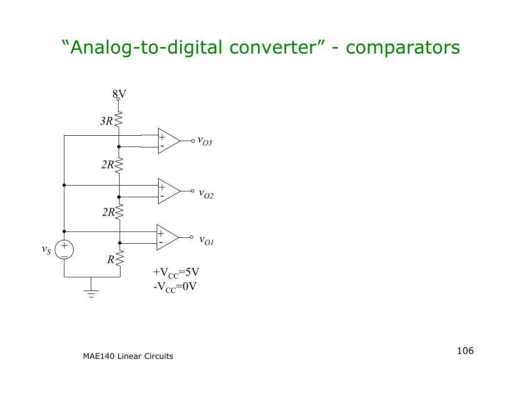
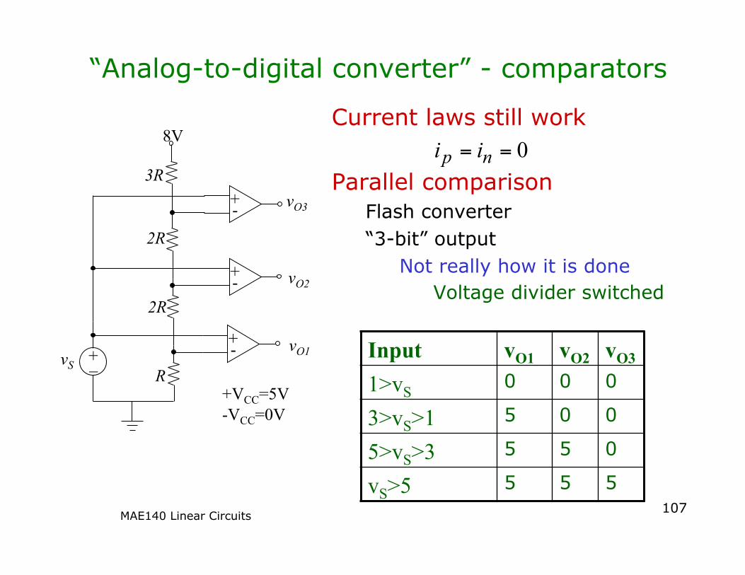
“Analog-to-digital converter” - comparators
+ _
2R
vS + -
+ -
+ -
3R
2R
R
vO1
vO2
vO3
8V
+VCC=5V -VCC=0V
MAE140 Linear Circuits 107
“Analog-to-digital converter” - comparators
Current laws still work
Parallel comparison Flash converter “3-bit” output
Not really how it is done Voltage divider switched
+ _
2R
vS + -
+ -
+ -
3R
2R
R
vO1
vO2
vO3
8V
+VCC=5V -VCC=0V
Input vO1 vO2 vO3 1>vS 0 0 0
3>vS>1 5 0 0
5>vS>3 5 5 0
vS>5 5 5 5
0== np ii
MAE140 Linear Circuits 108
OpAmp Circuit Design – the whole point
Given an input-output relationship design a cct to implement it Build a cct to implement vO=5v1+10v2+20v3
MAE140 Linear Circuits 109
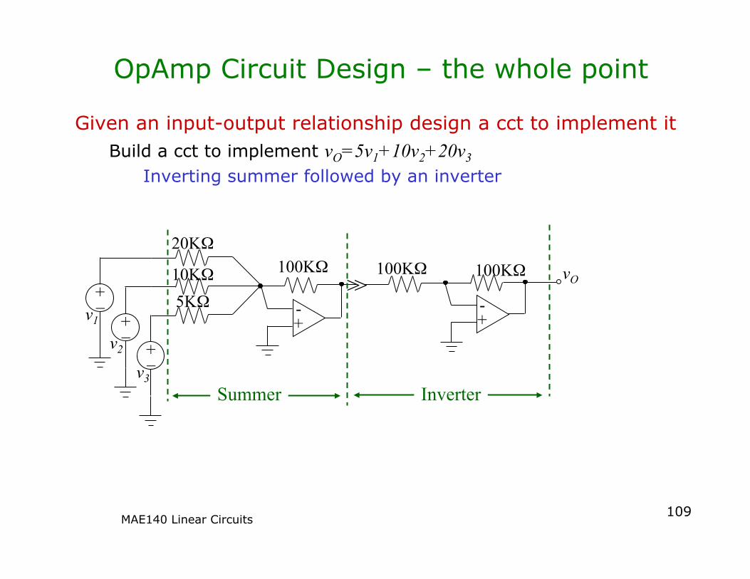
OpAmp Circuit Design – the whole point
Given an input-output relationship design a cct to implement it Build a cct to implement vO=5v1+10v2+20v3
Inverting summer followed by an inverter
+ _
20KΩ
v1 + - + -
+ _
+ _
v2
v3
10KΩ 5KΩ
100KΩ > >
100KΩ 100KΩ vO
Summer Inverter
MAE140 Linear Circuits 110
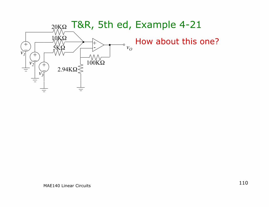
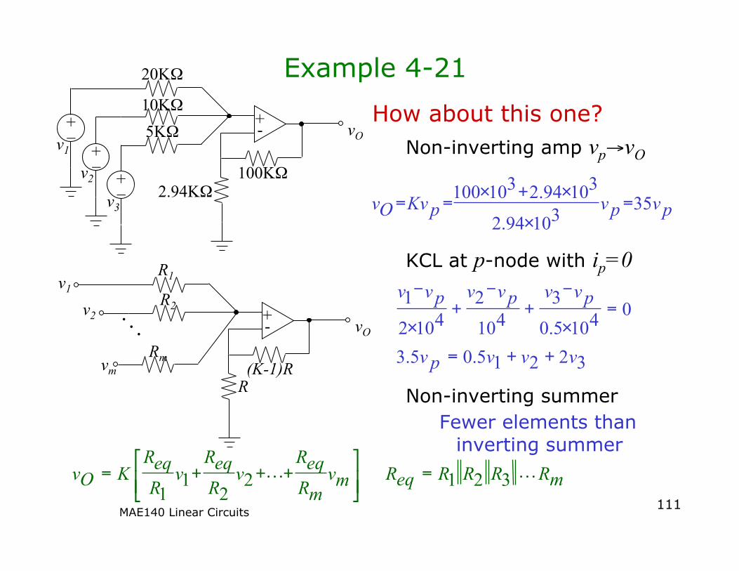
T&R, 5th ed, Example 4-21
+ _
20KΩ
v1 + _
+ _
v2
v3
10KΩ 5KΩ
100KΩ
+ - vO
2.94KΩ
How about this one?
MAE140 Linear Circuits 111
Example 4-21
How about this one? Non-inverting amp vp→vO
KCL at p-node with ip=0
Non-inverting summer Fewer elements than
inverting summer
+ _
20KΩ
v1 + _
+ _
v2
v3
10KΩ 5KΩ
100KΩ
+ - vO
2.94KΩ p v p v p Kv O v 35 3 10 94 . 2
3 10 94 . 2 3 10 100 = ×
× + × = =
- -
3 2 2 1 5 . 0 5 . 3
0 4 10 5 . 0 3
4 10 2
4 10 2 1
v v v p v
p v v p v v p v v
+ + =
= ×
+ + × -
R1 v1 v2
vm
+ - vO
R2
Rm (K-1)R
R
m R R R R eq R m v m R eq R
v R eq R
v R eq R
K O v 3 2 1 2 2 1
1 = + + + =
MAE140 Linear Circuits 112
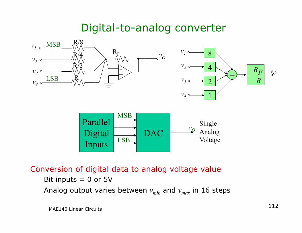
Digital-to-analog converter
Conversion of digital data to analog voltage value Bit inputs = 0 or 5V Analog output varies between vmin and vmax in 16 steps
R/8 v1
+ -
v2 R/4 R/2
RF vO
v3 v4
R
MSB
LSB
8
2
4
1
+
v1
v2
v3
v4
vO RFR−
Parallel Digital Inputs
DAC
MSB
LSB
vO Single Analog Voltage
MAE140 Linear Circuits 113
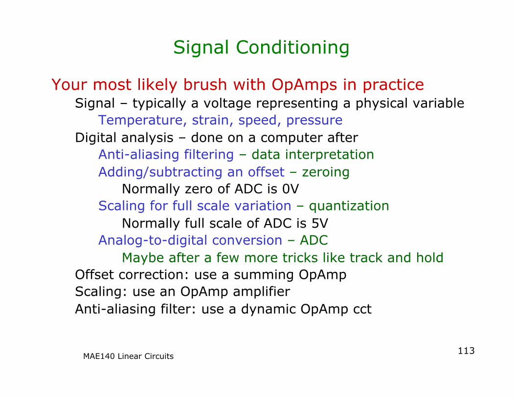
Signal Conditioning
Your most likely brush with OpAmps in practice Signal – typically a voltage representing a physical variable
Temperature, strain, speed, pressure Digital analysis – done on a computer after
Anti-aliasing filtering – data interpretation Adding/subtracting an offset – zeroing
Normally zero of ADC is 0V Scaling for full scale variation – quantization
Normally full scale of ADC is 5V Analog-to-digital conversion – ADC
Maybe after a few more tricks like track and hold Offset correction: use a summing OpAmp Scaling: use an OpAmp amplifier Anti-aliasing filter: use a dynamic OpAmp cct
MAE140 Linear Circuits 114
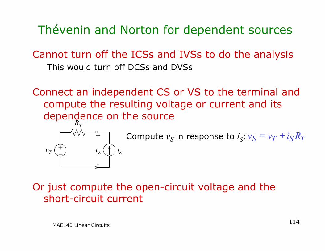
Thévenin and Norton for dependent sources
Cannot turn off the ICSs and IVSs to do the analysis This would turn off DCSs and DVSs
Connect an independent CS or VS to the terminal and compute the resulting voltage or current and its dependence on the source
Or just compute the open-circuit voltage and the short-circuit current
+ _
RT
vT iS vS
+
-
Compute vS in response to iS: T S T S R i v v + =
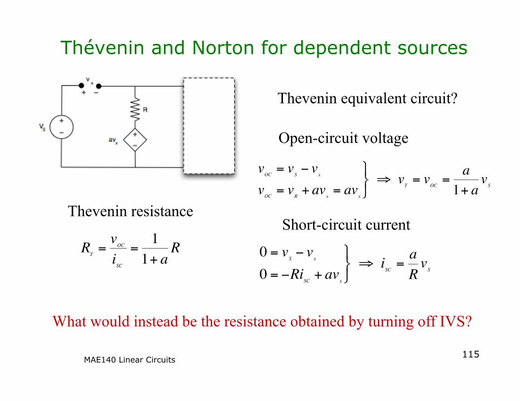
MAE140 Linear Circuits 115
Thévenin and Norton for dependent sources
Thevenin equivalent circuit?
€
vOC
= vS− v
x
vOC
= vR+ av
x= av
x
⇒ vT
= vOC
=a
1+ av
S
Open-circuit voltage
Short-circuit current
€
0 = vS− v
x
0 = −RiSC
+ avx
⇒ iSC
=aRv
S
€
RT
=v
OC
iSC
=11+ a
R
Thevenin resistance
What would instead be the resistance obtained by turning off IVS?
MAE140 Linear Circuits 116
Where to now?
Where have we been? Nodal and mesh analysis Thévenin and Norton equivalence Dependent sources and active cct models OpAmps and resistive linear active cct design
Where to now? Capacitors and inductors (Ch.6) Laplace Transforms and their use for ODEs and ccts (Ch.9)
s-domain cct design and analysis (Ch.10) Frequency response (Ch.12) and filter design (Ch.14)
We will depart from the book more during this phase


![Digital Chaotic Synchronized Communication System · coupled chaotic circuits and systems has been studied intensely [14] and some interesting applications such as broadband com-munication](https://img.pdfslide.us/doc/110x75/5e86a95e58f7f502e224fabc/digital-chaotic-synchronized-communication-coupled-chaotic-circuits-and-systems.jpg)