Embed Size (px)
Citation preview
Achievements and ResultsAnnual Report 2001

The double-axis articulated scanner is capable of directing light reflectedfrom a laser beam along variable paths an its x- and y- axis. If hundreds and thousands of such micro-mechanical elements are combined in opticalcross-connects, they can be used to switch data in a fiber-optic network.

Achievements and ResultsAnnual Report 2001
4 Fraunhofer ISIT Achievements and Results – Annual Report 2001
Preface............................................. 6
Profile of the InstituteBrief Portrait.................................... 11
Main Fields of Activity...................... 13
Offers for Research and ServiceService Offers...................................21
Customers....................................... 22
Innovation Catalogue.......................24
Representative FiguresBudget.............................................26
Staff Development........................... 27
The Fraunhofer-Gesellschaft at a GlanceThe Research Organization...............28
Location of the Research Establishments...................29
Representative Results of Work
IC-TechnologyApplication Specific Trench IGBTs..... 32
Array of Microguns for Parallel E-Beam Nanolithography...... 34
Microsystems TechnologyOptical MEMS for Telecommunication Networks...........36
MP-CC: A Competence Cluster for Silicon and Polymer Micro System Technologyin Schleswig-Holstein / Germany....... 37
Variable RF-MEMS Capacitors...........39
Digital Micromirror Arrays for Optical Switching.............................40
Resist Development Tool for Graytone Lithography................. 42
IC-DesignFinite Element Simulation of a RF-Switch..................................44
Development of Designkits forTechnology Dependent AcceleratedChipfinishing....................................45
Biotechnical MicrosystemsBio-MST Study “Detection of Biological Weapons”... 46
Module IntegrationA New Pilot Line for Wafer-Level-Packaging..................... 48
Manufacturing of an Optical Module for UV-Laser Ablation andPolishing the Cornea Surfaces ofHuman Eyes.....................................50
Rework of Electronic Assemblies...... 52
Important Names, Data, EventsLecturing Assignments at Universities.................................. 58
Memberships in Coordinationboardsand Committees............................... 58
Cooperation with Institutes andUniversities.......................................58
Trade Fairs and Exhibitions............... 59
Miscellaneous Events........................59
Scientific PublicationsJournal Papers and Contributions to Conferences.......... 60
Talks and Poster Presentations..........60
Diploma Theses................................62
General View on Projects..............63
Patents........................................... 64
Contact and Further Information....................................65
Imprint........................................... 65
Achievements and Results Annual Report 2001
Fraunhofer ISIT Achievements and Results – Annual Report 2001 5
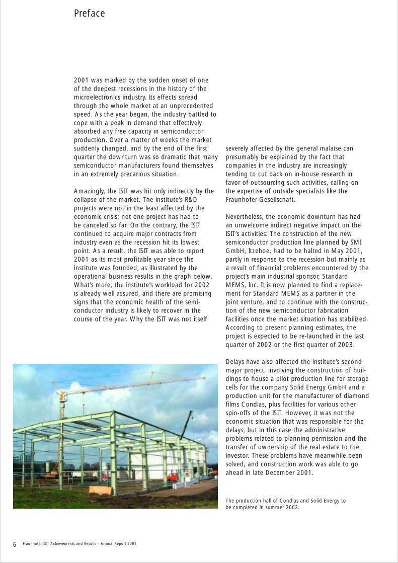
The production hall of Condias and Solid Energy to be completed in summer 2002.
6 Fraunhofer ISIT Achievements and Results – Annual Report 2001
2001 was marked by the sudden onset of one of the deepest recessions in the history of themicroelectronics industry. Its effects spreadthrough the whole market at an unprecedentedspeed. As the year began, the industry battled tocope with a peak in demand that effectivelyabsorbed any free capacity in semiconductor production. Over a matter of weeks the marketsuddenly changed, and by the end of the firstquarter the downturn was so dramatic that manysemiconductor manufacturers found themselvesin an extremely precarious situation.
Amazingly, the ISIT was hit only indirectly by thecollapse of the market. The institute’s R&D projects were not in the least affected by theeconomic crisis; not one project has had to be canceled so far. On the contrary, the ISIT continued to acquire major contracts from industry even as the recession hit its lowestpoint. As a result, the ISIT was able to report2001 as its most profitable year since the institute was founded, as illustrated by the operational business results in the graph below.What’s more, the institute’s workload for 2002 is already well assured, and there are promisingsigns that the economic health of the semi-conductor industry is likely to recover in the course of the year. Why the ISIT was not itself
severely affected by the general malaise can presumably be explained by the fact that companies in the industry are increasingly tending to cut back on in-house research in favor of outsourcing such activities, calling onthe expertise of outside specialists like theFraunhofer-Gesellschaft.
Nevertheless, the economic downturn has hadan unwelcome indirect negative impact on theISIT’s activities: The construction of the new semiconductor production line planned by SMIGmbH, Itzehoe, had to be halted in May 2001,partly in response to the recession but mainly asa result of financial problems encountered by theproject’s main industrial sponsor, StandardMEMS, Inc. It is now planned to find a replace-ment for Standard MEMS as a partner in thejoint venture, and to continue with the construc-tion of the new semiconductor fabrication facilities once the market situation has stabilized.According to present planning estimates, theproject is expected to be re-launched in the lastquarter of 2002 or the first quarter of 2003.
Delays have also affected the institute’s secondmajor project, involving the construction of buil-dings to house a pilot production line for storagecells for the company Solid Energy GmbH and aproduction unit for the manufacturer of diamondfilms Condias, plus facilities for various otherspin-offs of the ISIT. However, it was not the economic situation that was responsible for thedelays, but in this case the administrative problems related to planning permission and thetransfer of ownership of the real estate to theinvestor. These problems have meanwhile beensolved, and construction work was able to goahead in late December 2001.
Preface
Fraunhofer ISIT Achievements and Results – Annual Report 2001 7
A satisfactory solution has ultimately also beenfound for the ISIT, whereby the investor hasagreed to integrate workspace for spin-offs fromthe ISIT successively on a modular basis. The twocompanies involved are now waiting impatientlyfor the building work to be completed in thespring of 2002. They were both able to securethe necessary funds for the first stage of construction in 2001, and as a result the firstproduction plant is also ready for installation inthe building, as soon as it is finished. SolidEnergy intends to install a pilot production linefor lithium storage cells for the telecommunica-tions industry, with an output of around 5 milliondevices per year. Condias GmbH will be settingup a production unit for the manufacture of conductive diamond films (diamond-like carbonfilm), which have potential uses in a large number of applications.
One of the more interesting possible uses ofthese diamond films is in waste treatmentsystems for effluents that are difficult to disposeof or break down. The company’s electrolyticprocess based on conductive diamond layers is capable of breaking down even the most stable compounds. On the customer side, a consortium composed of almost all of Germany’sdockyards is intending to build sewage plants formarine vessels where bilge water (the mixed-composition polluted waste water that collects in the hull of ships) can be processed in an environmentally sound manner, rather than beingdischarged into the ocean, as at present. Condias GmbH is a spin-off of the FraunhoferInstitute for Surface Engineering and Thin Films(IST) in Braunschweig, set up jointly by the ISTand the ISIT in Itzehoe. In this connection, I would like to express my deepest thanks to thestaff of the IST, and especially to ProfessorBräuer, for their cooperation.
Another company, eBiochip GmbH, which worksin the field of electrical biochips, has also startedto establish a presence in the market in terms ofturnover. Its success, and the results of manyprojects in this field being worked on at the ISIT,are an indication that the time has now come forelectrical biochips to begin to find their first prac-tical applications in the detection of DNA/RNA,proteins and haptenes. eBiochip’s business isbased on the further development and produc-tion of detection systems based on biochipsdeveloped at the ISIT. I am convinced that theresearch market currently being served byeBiochip will soon turn into an end-user market.
There is good news to report in the field of inter-connection and packaging techniques. A separa-te department for interconnection and packagingtechniques, AVT, has been set up at the ISITthrough the integration of the former Centrumfür Mikroverbindungstechnik, CEM gGmbH in
Bund/Projektträger 6,2 %
Land Schleswig-Holstein 4 %
Sonstige 2,5 %
Industrie 77,6 %
EU 9,7 %
Ertragsgruppe Betrag in kEuro
Industrie 13.779
EU 1.714
Land Schleswig-Holstein 718
Bund/Projektträger 1.097
Sonstige 439
Summe Erträge BHH 17.747
Grundfinanzierung BHH -448
Aufwand BHH 17.299
Wirtschaftsdaten Budget zum Betriebshaushalt 2001
8 Fraunhofer ISIT Achievements and Results – Annual Report 2001
Neumünster. The merger was completed in 2001and CEM gGmbH was officially wound up in theautumn of 2001. The company’s former owners,the “Deutsche Verband für Schweißen und ver-wandte Verfahren”, DVS, and the “Fachverbandfür Sensorik”, AMA, have transferred their originalinvestment to the ISIT as a donation, for which Iwould like to thank them most sincerely. The new department for interconnection andpackaging techniques at the ISIT has greatlyexpanded with respect to the number of staffemployed by CEM gGmbH in Neumünster, and isnow operating on the lines of the Fraunhoferfunding model, predominantly through industrialsources of revenue. Special emphasis has beenplaced on expanding the services provided tosmall and medium-sized firms in the electronics-processing industry in Schleswig-Holstein. The AVT department at present generates anannual turnover of 1 million Euro from minor service contracts, mainly related to the solving of
Preface
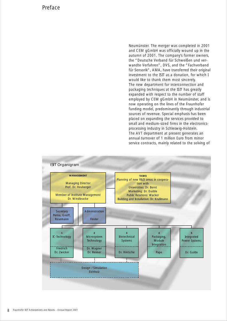
1
IC-Technology
FriedrichDr. Zwicker
SecretaryPerna, Greiff,
Rosemann
MANAGEMENT
Managing DirectorProf. Dr. Heuberger
Member of Institute ManagementDr. Windbracke
Design / SimulationEichholz
2
MicrosystemTechnology
Dr. WagnerDr. Reimer
Administration
Finder
TASKS
Planning of new R&D areas in coopera-tion with
Universities: Dr. BerntMarketing: Dr. Dudde
Public Relations: WackerBuilding and Installation: Dr. Krullmann
4
Packaging,Module
Integration
Pape
5
IntegratedPower Systems
Dr. Gulde
3
BiotechnicalSystems
Dr. Hintsche
ISIT Organigram
Fraunhofer ISIT Achievements and Results – Annual Report 2001 9
soldering problems in the manufacture of electronic modules or circuit assemblies.The problem of recruiting qualified staff hasbecome much less acute in 2001 as a result ofthe recession, but it is still almost impossible tofind suitable candidates in certain specialistfields, for instance circuit designers. Here, theGerman government’s “green card” initiative,which relaxes the conditions for the acquisitionof work and residence permits for certain cate-gories of non-EU citizens, is beginning to have apositive effect – there are now 5 members ofstaff at the ISIT who have benefited from thisarrangement. Nevertheless, we have to expectfurther full-scale confrontations with this problem, for instance when the second semiconductor manufacturing facility is expanded.It remains an urgent request that political decision-makers work towards creating more flexible conditions in the labor market, ratherthan acerbating the situation by bowing to short-sighted trade-union pressure or imposingexcessive bureaucratic restrictions.
Meanwhile, the ISIT continues to persevere in itsefforts to give young people a taste for the fieldsof microelectronics, microsystems engineering and microengineering at an early stage in theireducation. Noteworthy activities include a jointlobbying initiative with the comprehensive vocational training center in Itzehoe, in an effortto establish “microtechnologist” as an officialcategory in the German registry of recognizedtraining professions. This initiative is complemen-ted by the institute’s practice of offering sponso-red, paid placements to students at participatingschools/colleges, allowing them to gain workexperience at the ISIT during academic vacations.Both schemes are in such great demand that theISIT is rapidly reaching the limits of its capacity.
Overall, despite the recession in the semiconductorindustry, 2001 was a highly satisfactory year forthe ISIT. Once again, it was demonstrated thatthe ISIT’s new operating philosophy responds tothe needs of industry, and is much appreciatedby its customers. The key feature of this conceptis that the ISIT, in collaboration with its partnersin industry, is capable of offering a completerange of services, from the development of newsystems and the construction of demonstration
and test models through to series production.Now that the ISIT no longer employs inefficientlyutilized laboratory technology for its specializedservices, but instead makes use of cost-optimized,qualified and certified industrial manufacturingprocesses from the outset, the institute is also ina position to compete on costs.
Thanks to the commitment and outstanding efforts of the highly qualified experts working forthe ISIT and its partners, it has been possible tosuccessfully translate this theory into practice,and for this I would like to express my mostheartfelt gratitude to everyone involved in theseprojects.
Anton Heuberger
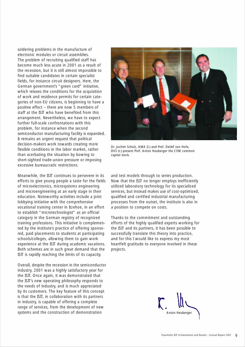
Dr. Jochim Scholz, AMA (l.) and Prof. Detlef von Hofe, DVS (r.) present Prof. Anton Heuberger the CEM commoncapital stock.
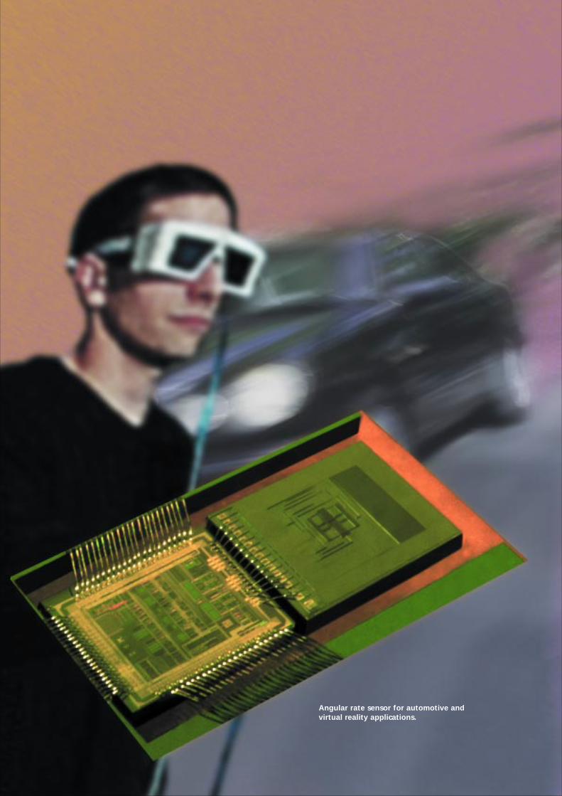
Angular rate sensor for automotive and virtual reality applications.
12 Fraunhofer ISIT Achievements and Results – Annual Report 2001
Main fields of Activity
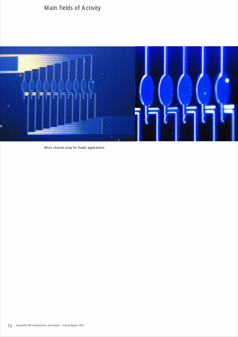
Micro channel array for fluidic applications.
Fraunhofer ISIT Achievements and Results – Annual Report 2001 13
IC-Technology
The IC-Technology department is focused on the development and fabrication of active andpassive silicon based devices.
In the field of active devices IGBTs, PowerMOSand diodes are of special importance. Here, ISITcan rely on a qualified core technology for powerdevices provided by our industrial partner.Customer specific development of power devicesis supported by simulation, design and electricalcharacterisation.
Further, ISIT has many years of experience in developing advanced CMOS processes with appropriate simulation and circuit designcapability.
Passive components like chip-capacitors, -resis-tors and -coils are another field of ISIT activities.Evaluation of new materials and its integration incomplete processes is one important topic forpassive IC development.
In addition ISIT offers customer specific waferprocessing in small and medium quantities based on standard IC and MST technology. This includes the development of new single processes and process modules for all relevantfields of semiconductor technology.
Detlef Friedrich+49(0)4821 / 17-4301email: [email protected]
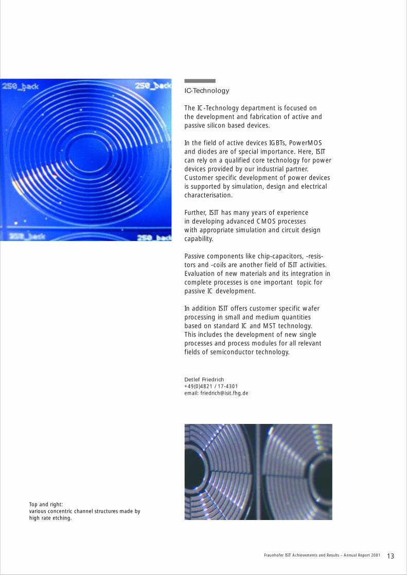
Top and right:various concentric channel structures made by high rate etching.
14 Fraunhofer ISIT Achievements and Results – Annual Report 2001
Chemical-Mechanical Polishing
Planarisation by means of chemical-mechanicalpolishing (CMP) is a key process for the fabri-cation of advanced ICs. The institute’s CMP application lab is equipped with CMP clustertools, single- and double-sided polishers andpost-CMP cleaners for substrate diameters of upto 300 mm and offers services on all aspects of CMP development like
• Testing of CMP equipment• Development of CMP processes for
- dielectrics (oxide, low-k materials, ...)- metals (tungsten, copper, ...)- silicon
• Testing of polishing slurries and pads• Post-CMP cleaning• CMP-related measurement• Custom-specific CMP services for device
manufacturing
In the field of CMP ISIT co-operates closely withequipment and pad/slurry manufacturers, pro-duction CMP users and the wafer industry.
Dr. Gerfried Zwicker+49(0)4821 / 17-4309email: [email protected]
IC-Design
Besides the main tasks of designing and testingmixed-signal ASICs, mainly in co-operation with in-house departments for microsystem development, the IC-Design department offersthe design of micromechanical and microopticalelements using analogue HDL for modelling andIC-layout and IC-verification tools.
State of the art IC-Design, FEM, and mathematicssoftware is used. For test purposes laboratoriesequipped with hardware for electrical measure-ments in time and frequency domain and for mechanical and optical standard tests areavailable.
Jörg Eichholz+49 (0) 4821 / 17 - 4537email: [email protected]
Main fields of Activity
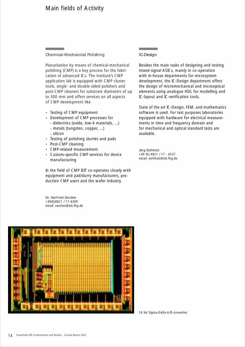
16 bit Sigma-Delta-A/D-converter.
Fraunhofer ISIT Achievements and Results – Annual Report 2001 15
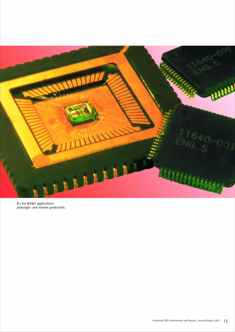
ICs for MEMS applications: prototype- and volume production.
Bildunterschriften?
16 Fraunhofer ISIT Achievements and Results – Annual Report 2001
Microsystems – MEMS
The MEMS department focuses on the applicationspecific development of optical, mechanical, fluidic, and RF-MEMS components and the integration to microsystems. We have access tothe 6-inch silicon frontend technology of the in-house industrial semiconductor production.Specific MEMS processes, such as wet etchingand deep RIE of Si, deposition of non-IC-compa-tible materials, thick resist lithography, grey-scalelithography, electroplating, replication technologies,wafer bonding and chemical-mechanical polishingare available in a separate cleanroom.
The optical MEMS activities are driven by applica-tions for optical communication and measuringsystems. Examples are fiber-optic switchingsystems, laser scanners, digital micromirror arrays,spectrometers, and also passive optical compo-nents , e.g. refractive and diffravtive microlenses.RF-MEMS components, such as RF-switches, tuna-ble capacitors and micro-relays are developed forwireless communication applications. Examples offluidic microsystems are pneumatic microvalves,sensor-controlled micro-pipettes and micropumps.The physical sensor group focuses on mechanicalsensors, especially angular rate, acceleration and pressure, and on thermal sensors. In theEUROPRACTICE frame we offer design-house service also for external MEMS foundry processes.The MEMS department works in close collaborationwith the ASIC-Design and the packaging departments in order to offer integrated micro-system solutions.
Dr. Bernd Wagner+49 (0) 48 21 / 17-42 23email: [email protected]
Dr. Klaus Reimer+49 (0) 48 21 / 17 45 06email: [email protected]
Biotechnical Microsystems
The department Biotechnical Microsystems of isfocusing its activities in the field of electrical bio-sensor technologies. Our activities aim at thedesign and construction of novel sensing arraysin miniaturized formats. The development of socalled ultramicroelectrodes enable novel sensorconstructions and the evaluation of highly sensi-tive and new approaches of selective detectingprinciples, e.g. the redox recycling.
The integration of transducers made in silicontechnology and microfluidic systems with activemanipulation of biomolecules opens new appli-cations in biochemical assays, medical diagnosticsand environmental analytics.
Sub-µm-electrode arrays have been developed as a widely applicable technology platform for analytic approaches. In combination withmicrofluidic components on chip and miniaturizedor integrated electronics these components formthe basis of smart portable analytical systems.
The department Biotechnical Microsystems offersR&D and services in the multi-channel sensorarray technology as an attractive feature for fullyelectrical DNA and protein chips. Also a novelmicromachined glucose sensor enables long termonline monitoring of human body fluids. Such biochips may be used as parts of ”lab-on-chips” and micro-total analysis systems.For market activities a spin off company (www. ebiochipsystems.com) have been positioned to improve the way of biochemicaland molecular biological analysis.
Dr. Rainer Hintsche+ 49 (0) 48 21/ 17-42 21email: [email protected]
Main fields of Activity
Fraunhofer ISIT Achievements and Results – Annual Report 2001 17
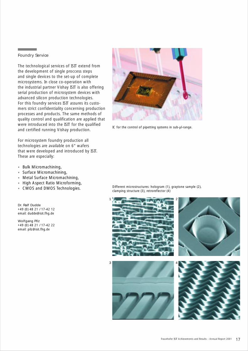
Foundry Service
The technological services of ISIT extend from the development of single proccess steps and single devices to the set-up of completemicrosystems. In close co-operation with the industrial partner Vishay ISIT is also offeringserial production of microsystem devices withadvanced silicon production technologies. For this foundry services ISIT assures its custo-mers strict confidentiality concerning productionprocesses and products. The same methods ofquality control and qualification are applied thatwere introduced into the ISIT for the qualifiedand certified running Vishay production.
For microsystem foundry production all technologies are available on 6‘‘ wafers that were developed and introduced by ISIT.These are especially:
• Bulk Micromachining,• Surface Micromachining,• Metal Surface Micromachining,• High Aspect Ratio Microforming,• CMOS and DMOS Technologies.
Dr. Ralf Dudde+49 (0) 48 21 / 17-42 12email: [email protected]
Wolfgang Pilz+49 (0) 48 21 / 17-42 22email: [email protected]
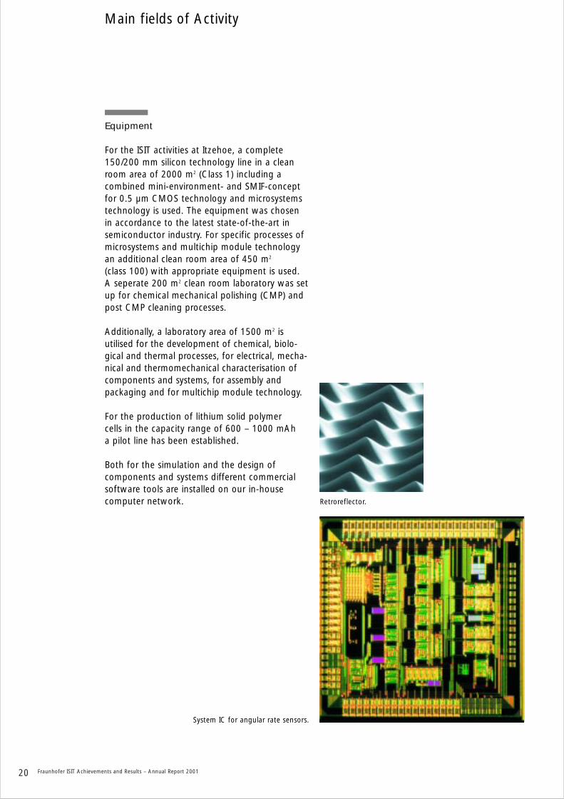
Different microstructures: hologram (1), graytone sample (2),clamping structure (3), retroreflector (4)
1 2
3 4
IC for the control of pipetting systems in sub-µl-range.
18 Fraunhofer ISIT Achievements and Results – Annual Report 2001
Assembly and Packaging Technology forMicrosystems, Sensors and Multichip Modules
In advanced packaging technology ISIT focuseson wafer level packaging (WLP) and direct chipattach techniques for multichip modules (MCMs)and for MEMS components. For WLP a 150 mmwafer pilot line for small to medium volume runshas been established with following features:under bump metallization, BCB passivation, bumping, grinding, backsite metallization, parameter test and dicing. The bonding of baredice and microsensors is realised by applyingchip-on-board (COB) and especially flip-chiptech-nology, where bare ICs are mounted andsimultaneously interconnected face down ontothe substrate. The processes available at ISITinclude wafer preparation with chemical depo-sition of NiAu, different bumping techniques(printed solder bumps, Au stud bumps), flip-chipplacement and inter-connection by adhesive joining or soldering. Furthermore, ISIT deals withmounting and packaging technology of powerelectronic components and modules.
Standard processes for hermetic package sealing are available, e.g. metallic packages aresealed by laser welding in inert gas atmosphere.Furthermore, ISIT works on wafer level encap-sulation of MEMS devices using glass frit andmetallic seal bonding. Automatic equipment facilitates to enable the production of demons-tration series under industrial conditions.
Karin Pape+49(0)48 21 / 17-42 29email: [email protected]
Thomas Harder+49(0)48 21 / 17-46 20email: [email protected]
Quality and Reliability of Microelectronic Assemblies
The main competence is attributed to the evalu-ation of the manufacturing quality and the reliability of microelectronic assemblies andmodules including the as-delivered quality ofcomponents and circuit boards. Methods aredestructive metallographic as well as nondestructive (e.g. x-ray) principles. The evaluationof the long-time behaviour of the assemblies isbased on the matrix of requirements using modelcalculations, environmental and load tests up tofailure analyses. For optimisation of manufac-turing processes the institute applies processmodels and fabricates samples on in-line equipment including mass production as well asrework systems. Furthermore, in the field of thermal management and reliability ISIT works on customer specific power modules.
Karin Pape+49(0)48 21 / 17-42 29email: [email protected]
Dr. Thomas Ahrens+49(0)48 21 / 17-46 05email: [email protected]
Main fields of Activity
Fraunhofer ISIT Achievements and Results – Annual Report 2001 19
Integrated Power Systems
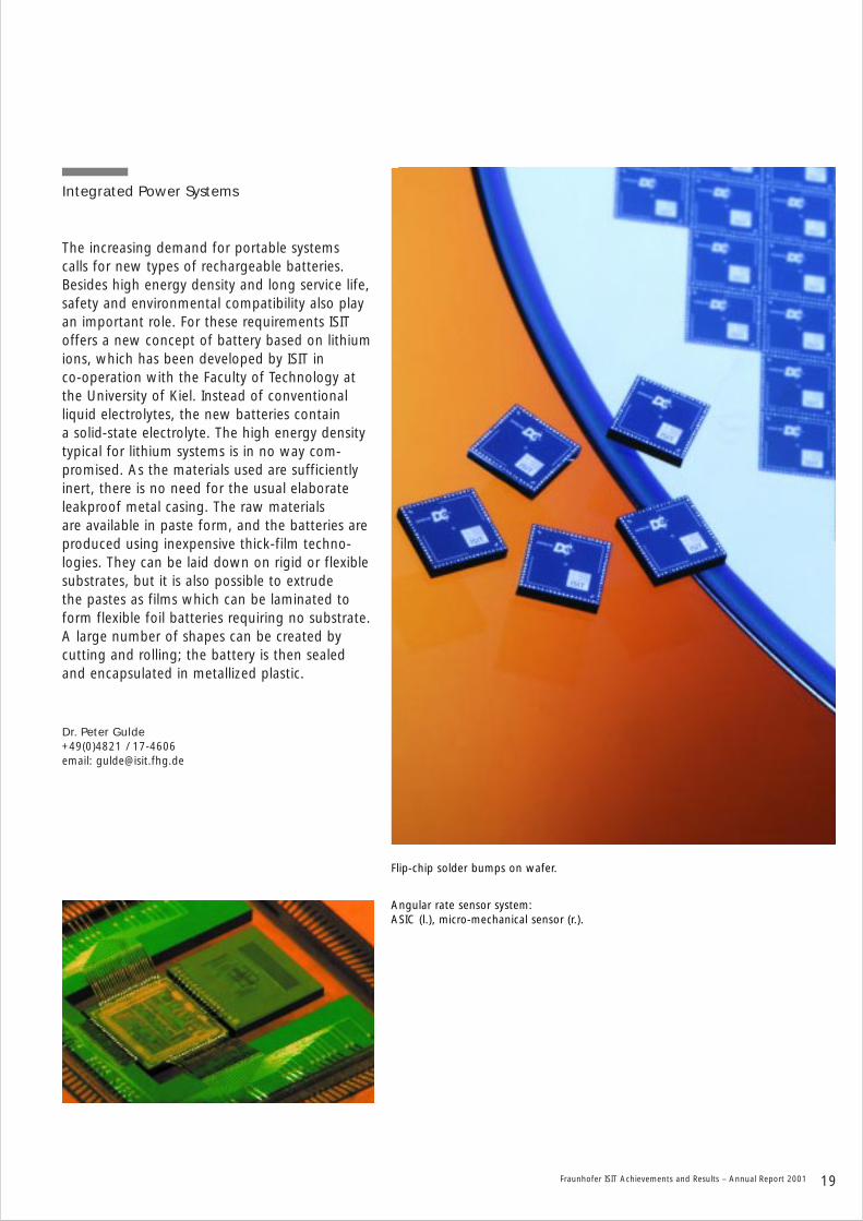
The increasing demand for portable systems calls for new types of rechargeable batteries.Besides high energy density and long service life,safety and environmental compatibility also playan important role. For these requirements ISIToffers a new concept of battery based on lithiumions, which has been developed by ISIT in co-operation with the Faculty of Technology atthe University of Kiel. Instead of conventionalliquid electrolytes, the new batteries contain a solid-state electrolyte. The high energy densitytypical for lithium systems is in no way com-promised. As the materials used are sufficientlyinert, there is no need for the usual elaborateleakproof metal casing. The raw materials are available in paste form, and the batteries are produced using inexpensive thick-film techno-logies. They can be laid down on rigid or flexiblesubstrates, but it is also possible to extrude the pastes as films which can be laminated toform flexible foil batteries requiring no substrate.A large number of shapes can be created by cutting and rolling; the battery is then sealed and encapsulated in metallized plastic.
Dr. Peter Gulde+49(0)4821 / 17-4606email: [email protected]
Flip-chip solder bumps on wafer.
Angular rate sensor system: ASIC (l.), micro-mechanical sensor (r.).
20 Fraunhofer ISIT Achievements and Results – Annual Report 2001
Retroreflector.
Equipment
For the ISIT activities at Itzehoe, a complete150/200 mm silicon technology line in a cleanroom area of 2000 m2 (Class 1) including a combined mini-environment- and SMIF-conceptfor 0.5 µm CMOS technology and microsystemstechnology is used. The equipment was chosenin accordance to the latest state-of-the-art insemiconductor industry. For specific processes ofmicrosystems and multichip module technologyan additional clean room area of 450 m2
(class 100) with appropriate equipment is used.A seperate 200 m2 clean room laboratory was setup for chemical mechanical polishing (CMP) andpost CMP cleaning processes.
Additionally, a laboratory area of 1500 m2 is utilised for the development of chemical, biolo-gical and thermal processes, for electrical, mecha-nical and thermomechanical characterisation ofcomponents and systems, for assembly and packaging and for multichip module technology.
For the production of lithium solid polymer cells in the capacity range of 600 – 1000 mAh a pilot line has been established.
Both for the simulation and the design of components and systems different commercialsoftware tools are installed on our in-house computer network.
System IC for angular rate sensors.
Main fields of Activity

Fraunhofer ISIT Achievements and Results – Annual Report 2001 21
Service Offers
Microelectronic components andmicrosystems are used in a multitudeof products.
The institute offers its service to different branches of industry and cooperates with small and mediumsized firms as well as with big companies.
From single components to completesystems ISIT offers design, simulationand manufacturing to their customers.The customers specifies the field ofapplication of the desired productsand the profile of requirements.
The execution of the tasks is accom-plished in close cooperation with the client. After the realisation ofdemonstration models and prototypes,the technology developed within theproject will be transferred to thecustomer. Confidentiality of results andexchanged intellectual property isensured.
The services of ISIT are very profitablefor small- and medium-sized enter-prises which cannot afford the bigcapital investments of a technologicalinfrastructure. They can utilise thecompetence of the institute for development, testing and introductionof necessary technological innovations.
The auditorium and lecture rooms of ISIT cover an area of circa 1000 m2
and are available for conferences,workshops and other events for up to400 participants.
Service Offers of ISIT in Detail
Studies for development of appli-cation-specific sensors, actuators, optical and mechanical components,microsystems, MCMs as well as for the basics of future integration tech-nologies.
Contract research for the developmentof demonstrators to verify the feasibili-ty of components and systems.
Production of prototypes of integratedsubsystems for the development ofsystems and products.
Design and manufacturing of com-ponents and assemblies in pilot- andcustomer specific series by ISIT.
Design of components and systemsutilising industrial foundries (analogue/mixed-signal ASICs and microsystems).
Transfer of the developed technologies,components and subsystems to indus-trial technology suppliers for the production phase or the manufacturingin ISIT following industrial quality standards, respectively.
Development of production tools and process technologies for the fabrication of semiconductors andmicrosystems in co-operation withequipment manufacturers.
Development of individual processesfor the production of integrated circuits and microsystems.
Integration of semiconductor com-ponents with biological materials.
Module integration of microelectronicsystems and preparation of sampleseries for MCM and Chip-Size packages(CSP).
Mounting and packaging technologiesfor microsystems, sensors and MCMs.
Evaluation of quality and reliability ofmicroelectronic assemblies and powermodules.
Failure and process analysis in soldering technology.
Consulting and support for setting uptechnological production facilities.
Technology-oriented seminars with practical training sessions andcustomer specific in-house courses.
Offers for Research and Service
22 Fraunhofer ISIT Achievements and Results – Annual Report 2001
Customers
ISIT cooperates with companies of different sectors and sizes. In the following some companies are presented as a reference:
Bullith Batteries AG, München
Bundesanstalt für Materialforschung und -prüfung,Berlin
Braun AG, Kronberg
CamLine, Petershausen
C – MAC Electromag n.v. Ronse, Belgium
Conti Temic, Ottobrunn
Continental AG, Hannover
Contrade GmbH, Wiernsheim
Corning Frequency ControlGmbH & Co. KG,Neckarbischofsheim
Creavis GmbH, Marl
Daimler Benz Aerospace, Bremen
Danfoss Lighting Controls,Nordborg, Denmark
Danfoss Drives, Graasten, Denmark
Danfoss Silicon Power, Nortorf
Danfoss Silicon Power GmbH,Schleswig
Datacon, Radfeld/Tirol
Decker Anlagenbau GmbH, Berg
Degussa AG, Hanau
Detectomat Brandmeldesysteme GmbH,Timmendorfer Strand
Disetronic Medical Systems AG,Burgdorf, Switzerland
Dräger Pro Tech GmbH, Lübeck
D-Tech GmbH, Bielefeld
EADS, Ottobrunn
EADS, Ulm
Easylab, Itzehoe
eBiochip Systems GmbH, Itzehoe
Eppendorf-Netheler-Hinz GmbH,Hamburg
ESW-EXTEL Systems GmbH,Wedel
Evotec Biosystems GmbH,Hamburg
Fibronix, Kiel
Flextronics International,Althofen, Austria
Force Computers GmbH,Neubiberg
Fresnel Optics, Apolda
Fuba GmbH, Gittfelde
Heidelberger Druckmaschinen,Kiel
HL Planartechnik GmbH,Dortmund
IBM- Speichersysteme GmbH,Mainz
IC-Haus GmbH, Bodenheim
ICT, München
Implex GmbH, Ismaning/München
Infineon Technologies AG,München
ISiltec GmbH, Erlangen
ITT Automotive Europe GmbH,Eberhahn
Judex Datasystems A/S, Aalborg, Denmark
Kapsch, Wien, Austria
Kember Associates,Bristol, UK
Kendrion Binder Magnete GmbH, VS-Villingen
Kolbenschmidt Pierburg AG,Neuss
Kugler GmbH, Salem
Kuhnke GmbH, Malente
LEICA, Jena
Litef, Freiburg
Mannesmann VDO AG,Babenhausen
Offers for Research and Service
ABB, Heidelberg
Advanced Technology Line LTO.,Anyang City, Korea
Alcatel Kirk, Ballerup, DK
Alcatel, Stuttgart
APPLIED MATERIALS, Santa Clara,USA
Astrium, München
Atmel GmbH, Heilbronn
Atotech Deutschland GmbH,Berlin
Basler Vision Technologies,Ahrensburg
Bayer AG, Leverkusen
Becker Automotive Systems,Karlsbad
Beiersdorf AG, Hamburg
BERU, Ludwigsburg
BioGaia Fermentation AB(BioGaia), Lund, Sweden
Biotronik GmbH, Berlin
Bodenseewerk Gerätetechnik,Überlingen
Borg Instruments, Remchingen
Bosch Telecom GmbH, Backnang
Bosch, Reutlingen
Fraunhofer ISIT Achievements and Results – Annual Report 2001 23
Mannesmann VDO AG, Karben
Mair Elektronik GmbH, Neufahrn
Max Stegmann GmbH,Donaueschingen
microParts GmbH, Dortmund
Miele & Cie., Gütersloh
Minimax GmbH, Bad Oldesloe
Montronic-Schackmann GmbH,Rheinstetten
Motorola GmbH, Flensburg
mrt – Micro-Resist-Technology,Berlin
MST Systemtechnik GmbH,Doanuworth
m-u-t GmbH, Wedel
Nanophotonics AG, Mainz
Neutronics Althofen ElectronicsGmbH, Althofen, Austria
Nokia Research Center, Nokia Group, Helsinki, Finland
November AG, Erlangen
Novo ZYMES A/S (NOVO),Bagsvaerd, Denmark
NU-Tech GmbH, Neumünster
OK Media Disc ServiceGmbH & Co.KG, Nortorf
Orbis Technologies Ltd.,Branbury, UK
Orga Kartensysteme GmbH,Flintbeck
Oticon, A/S, Hellerup, Denmark
PAV Card GmbH, Lütjensee
PAS GmbH, Itzehoe
Pohlmann & Partner GmbH,Quickborn
Perkin Elmer Optoelectronics,Wiesbaden
Pharmacia & Upjoh AB(Pharmacia), Strängnäs, Sweden
Philips Semiconductors, Gratkorn
Philips Semiconductors, Hamburg
P. M. C. GmbH, Usingen
PräTEC GmbH, Rohr
Quintenz Hybridtechnik, Neuried bei München
Raytheon Anschütz GmbH, Kiel
Robert Bosch GmbH, Salzgitter
Scana Holography CompanyGmbH, Schenefeld
SEF GmbH, Scharnebek
SensLab GmbH, Leipzig
SensoNor, Horten, Norway
Sentech Instruments GmbH,Berlin
Sextant, Avionique, Valence, France
Siemens AG, Bocholt
Siemens AG, Zentrale Technik,Erlangen
Siemens AG, München
Siemens VDO Automotive AG,Karben
SMA Regelsysteme GmbH,Niestetal
Smith Meter GmbH, Ellerbeck
Solid Energy GmbH, Itzehoe
Sparkolor, Inc., Santa Clara, USA
ST Microelectronics, Mailand, Italy
Technolas, München
TELE QUARZ GmbH, Neckar-Bischofsheim
Temic microelectronic GmbH,Ottobrunn
Tesa AG, Hamburg
Thomson, Paris, France
Trelleborg GmbH, Werk 2,Neumünster
Tricumed GmbH, Kiel
Trioptics GmbH, Wedel
Tronics, Grenoble, France
VDMA Fachgemeinschaft Fluidtechnik, Frankfurt
Vega, Schiltach
Vishay, Holon, Israel
Vishay Semiconductor GmbH,Itzehoe
Mannesmann-VDO, Karben
Wabco Fahrzeugbremsen,Hannover
Peter Wolters CMP SystemeGmbH, Rendsburg
Woowon Technology, Korea
W. S. I. Wafer Service International, Evry Cedex, Paris, France
YAGEO EUROPE GmbH,Pinneberg
24 Fraunhofer ISIT Achievements and Results – Annual Report 2001
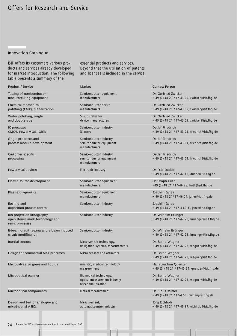
Product / Service Market Contact Person
Testing of semiconductor Semiconductor equipment Dr. Gerfried Zwickermanufacturing equipment manufacturers + 49 (0) 48 21 / 17-43 09, [email protected]
Chemical-mechanical Semiconductor device Dr. Gerfried Zwickerpolishing (CMP), planarization manufacturers + 49 (0) 48 21 / 17-43 09, [email protected]
Wafer polishing, single Si substrates for Dr. Gerfried Zwickerand double side device manufacturers + 49 (0) 48 21 / 17-43 09, [email protected]
IC processes Semiconductor industry Detlef FriedrichCMOS, PowerMOS, IGBTs IC-users + 49 (0) 48 21 / 17-43 01, [email protected]
Single processes and Semiconductor industry Detlef Friedrichprocess module development semiconductor equipment + 49 (0) 48 21 / 17-43 01, [email protected]
manufacturers
Customer specific Semiconductor industry Detlef Friedrichprocessing semiconductor equipment + 49 (0) 48 21 / 17-43 01, [email protected]
manufacturers
PowerMOS devices Electronic industry Dr. Ralf Dudde+ 49 (0) 48 21 / 17-42 12, [email protected]
Plasma source development Semiconductor equipment Christoph Huthmanufacturers +49 (0) 48 21 / 17-46 28, [email protected]
Plasma diagnostics Semiconductor equipment Joachim Janesmanufacturers + 49 (0) 48 21/ 17-46 04, [email protected]
Etching and Semiconductor industry Joachim Janesdeposition process control + 49 (0) 48 21 / 17-4 60 4l, [email protected]
Ion projection,lithography Semiconductor industry Dr. Wilhelm Brüngeropen stencil mask technology and + 49 (0) 48 21 / 17-42 28, [email protected] processes
E-beam circuit testing and e-beam induced Semiconductor industry Dr. Wilhelm Brüngercircuit modification + 49 (0) 48 21 / 17-42 28, [email protected]
Inertial sensors Motorvehicle technology, Dr. Bernd Wagnernavigation systems, measurements + 49 (0) 48 21 / 17-42 23, [email protected]
Design for commercial MST processes Micro sensors and actuators Dr. Bernd Wagner+ 49 (0) 48 21 / 17-42 23, [email protected]
Microvalves for gases and liquids Analytic, medical technology Hans Joachim Quenzermeasurement + 49 (0 ) 48 21 / 17-45 24, [email protected]
Microoptical scanner Biomedical technology, Dr. Bernd Wagneroptical measurement industry, + 49 (0) 48 21 / 17-42 23, [email protected]
Microoptical components Optical measurement Dr. Klaus Reimer+ 49 (0) 48 21 / 17-4 50, [email protected]
Design and test of analogue and Measurement, Jörg Eichholzmixed-signal ASICs automaticcontrol industry + 49 (0) 48 21 / 17-45 37, [email protected]
Innovation Catalogue
ISIT offers its customers various pro-ducts and services already developedfor market introduction. The followingtable presents a summary of the
essential products and services.Beyond that the utilisation of patentsand licences is included in the service.
Offers for Research and Service
Fraunhofer ISIT Achievements and Results – Annual Report 2001 25
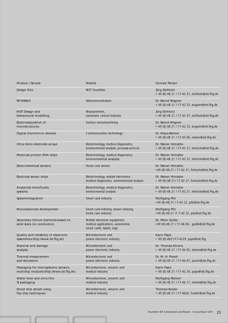
Product / Service Market Contact Person
Design Kits MST foundries Jörg Eichholz+ 49 (0) 48 21 / 17-45 37, [email protected]
RF-MEMS Telecommunication Dr. Bernd Wagner+ 49 (0) 48 21 / 17-42 23, [email protected]
MST Design and Measurement, Jörg Eichholzbehavioural modelling automatic control industry + 49 (0) 48 21 / 17-45 37, [email protected]
Electrodeposition of Surface micromachining Dr. Bernd Wagnermicrostructures + 49 (0) 48 21 / 17-42 23, [email protected]
Digital micromirror devices Communication technology Dr. Klaus Reimer+ 49 (0) 48 21 / 17-45 06, [email protected]
Ultra micro electrode arrays Biotechnology, medical diagnostics, Dr. Rainer Hintscheenvironmental analysis, process control + 49 (0) 48 21 / 17-42 21, [email protected]
Electrical protein DNA chips Biotechnology, medical diagnostics, Dr. Rainer Hintscheenvironmental analysis + 49 (0) 48 21 / 17-42 21, [email protected]
Electrochemical sensors Home care service Dr. Rainer Hintsche+49 (0) 48 21 / 17-42 21, [email protected]
Electrical sensor chips Biotechnology, related electronics Dr. Rainer Hintschemedical diagnostics, environmental analysis + 49 (0) 48 21/ 17-42 21, [email protected]
Analytical microfluidic Biotechnology ,medical diagnostics, Dr. Rainer Hintsche systems environmental analysis + 49 (0) 48 21 / 17-42 21, [email protected]
Systemintegration Smart card industry Wolfgang Pilz+49 (0) 48 21 / 7-42 22, [email protected]
Microelectrode development Smart card industry, sensor industry, Wolfgang Pilzhome care industry +49 (0) 48 21 /1 7-42 22, [email protected]
Secondary lithium batteries based on Mobile electronic equipment, Dr. Peter Guldesolid state ion conductors medical applications, automotive, +49 (0) 48 21 / 17-46 06, [email protected]
smart cards, labels, tags
Quality and reliability of electronic Microelectronic and Karin Pape assemblies (http://www.isit.fhg.de) power electronic industry + 49 (0) 4821/17-4229, [email protected]
Material and damage Microelectronic and Dr. Thomas Ahrensanalysis power electronic industry + 49 (0) 48 21 / 17-46 05, [email protected]
Thermal measurement Microelectronic and Dr. M. H. Poechand simulation power electronic industry + 49 (0) 48 21 / 17-46 07, [email protected]
Packaging for microsystems, sensors, Microelectronic, sensoric and Karin Papemultichip modules (http://www.isit.fhg.de) medical industry + 49 (0) 48 21 / 17-42 29, [email protected]
Wafer level and ultra thin Microelectronic, sensoric and Wolfgang Reinert Si packaging medical industry + 49 (0) 48 21 / 17-46 17, [email protected]
Direct chip attach using Microelectronic, sensoric and Thomas Harderflip chip techniques medical industry + 49 (0) 48 21 / 17-4620, [email protected]
26 Fraunhofer ISIT Achievements and Results – Annual Report 2001
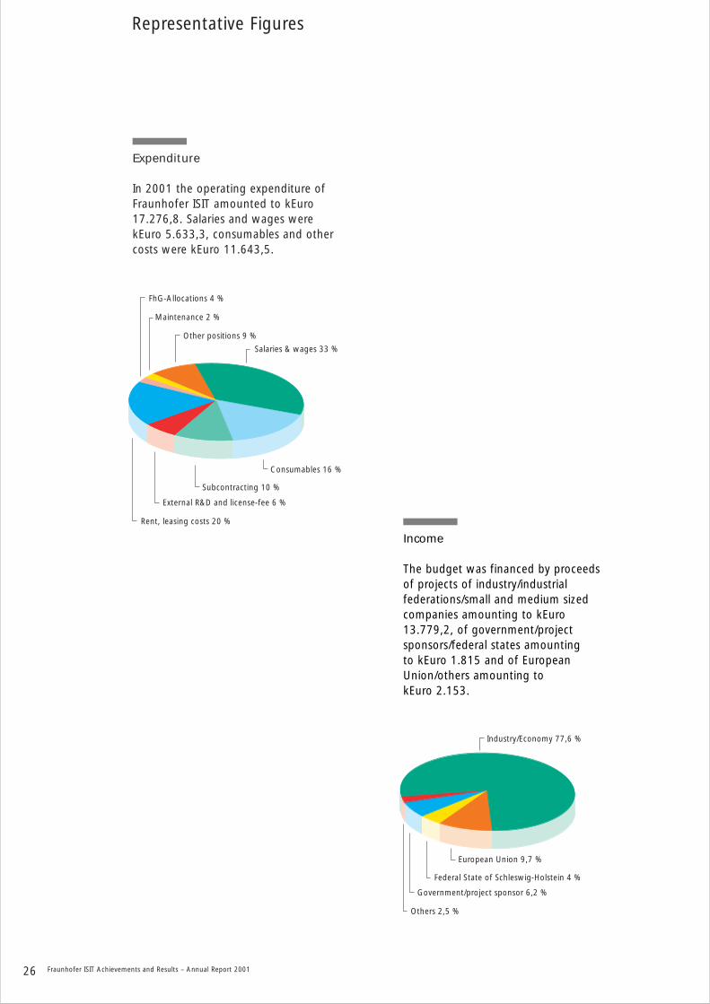
Expenditure
In 2001 the operating expenditure ofFraunhofer ISIT amounted to kEuro17.276,8. Salaries and wages werekEuro 5.633,3, consumables and othercosts were kEuro 11.643,5.
Representative Figures
Maintenance 2 %
Salaries & wages 33 %
Rent, leasing costs 20 %
External R&D and license-fee 6 %
Subcontracting 10 %
Consumables 16 %
Other positions 9 %
FhG-Allocations 4 %
Government/project sponsor 6,2 %
Industry/Economy 77,6 %
Federal State of Schleswig-Holstein 4 %
European Union 9,7 %
Others 2,5 %
Income
The budget was financed by proceedsof projects of industry/industrial federations/small and medium sizedcompanies amounting to kEuro13.779,2, of government/project sponsors/federal states amounting to kEuro 1.815 and of EuropeanUnion/others amounting to kEuro 2.153.
Fraunhofer ISIT Achievements and Results – Annual Report 2001 27
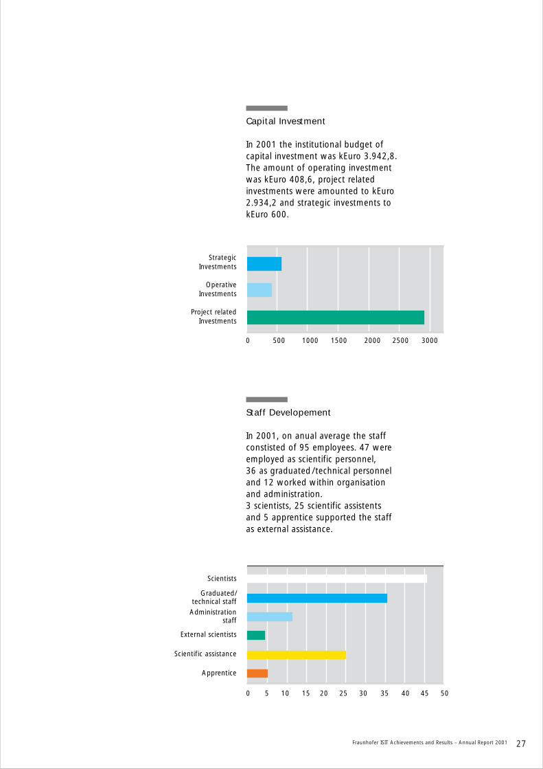
Scientists
Graduated/technical staff
Administrationstaff
External scientists
Scientific assistance
Apprentice
Capital Investment
In 2001 the institutional budget ofcapital investment was kEuro 3.942,8.The amount of operating investmentwas kEuro 408,6, project relatedinvestments were amounted to kEuro2.934,2 and strategic investments tokEuro 600.
StrategicInvestments
OperativeInvestments
Project relatedInvestments
2000 2500 3000500 1000 15000
50454035302520151050
Staff Developement
In 2001, on anual average the staffconstisted of 95 employees. 47 wereemployed as scientific personnel, 36 as graduated/ technical personneland 12 worked within organisationand administration. 3 scientists, 25 scientific assistentsand 5 apprentice supported the staffas external assistance.
28 Fraunhofer ISIT Achievements and Results – Annual Report 2001
The Fraunhofer-Gesellschaft
The Fraunhofer-Gesellschaft is the leading organization for institutes of applied research inEurope, undertaking contract research on behalfof industry, the service sector and the govern-ment. Commissioned by customers in industry, it provides rapid, economical and immediatelyapplicable solutions to technical and organi-zational problems. Within the framework of theEuropean Union’s technology programs, theFraunhofer-Gesellschaft is actively involved inindustrial consortiums which seek technical solutions to improve the competitiveness ofEuropean industry.
The Fraunhofer-Gesellschaft also assumes amajor role in strategic research: Commissionedand funded by Federal and Länder ministries and governments, the organization undertakesfuture-oriented research projects which contri-bute to the development of innovations in spheres of major public concern and in key technologies. Typical research fields include communications, energy, microelectronics, manufacturing, transport and the environment.
The global alignment of industry and researchhas made international collaboration imperative.Furthermore, affiliate Fraunhofer institutes inEurope, in the USA and in Asia ensure contact tothe most important current and future economicmarkets.
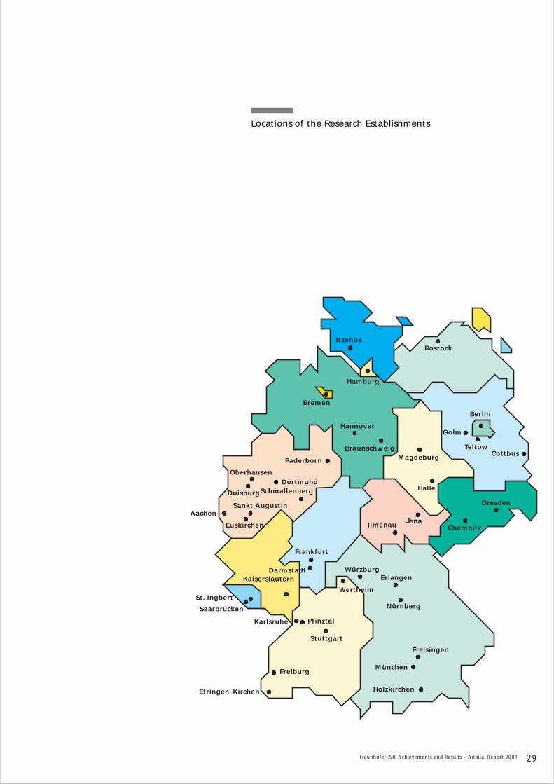
At present, the organization maintains 56 researchestablishments at locations throughout Germany.A staff of some 11,000 – the majority of whomare qualified scientists and engineers – generatethe annual research volume of more than 900million. Of this amount, over 800 million is derivedfrom contract research. Research contracts onbehalf of industry and publicly financed researchprojects generate approximately two thirds of theFraunhofer-Gesellschaft’s contract revenue. One third is contributed by the Federal andLänder governments, as a means of enabling the institutes to work on solutions to problemsthat are expected to attain economic and socialrelevance in the next five to ten years.
Fraunhofer scientists specialize in complex research tasks involving a broad spectrum ofresearch fields. When required, several institutespool their interdisciplinary expertise to developsystem solutions.
The Fraunhofer-Gesellschaft was founded in1949 and is a recognized non-profit organization.Its members include well-known companies andprivate patrons who contribute to the promotionof its application-oriented policy.
The organization takes its name from Joseph vonFraunhofer (1787-1826), the successful Munichresearcher, inventor and entrepreneur.
The Fraunhofer-Gesellschaft at a Glance
Fraunhofer ISIT Achievements and Results – Annual Report 2001 29
Paderborn
ItzehoeRostock
Bremen
Hamburg
Berlin
CottbusTeltow
Golm
Magdeburg
Halle
Dresden
ChemnitzJenaIlmenau
WürzburgErlangen
Nürnberg
Wertheim
Braunschweig
Hannover
OberhausenDortmund
SchmallenbergDuisburg
AachenSankt Augustin
Euskirchen
Frankfurt
Darmstadt
St. Ingbert
Saarbrücken
Kaiserslautern
PfinztalKarlsruhe
Stuttgart
Freiburg
Efringen–Kirchen
Freisingen
München
Holzkirchen
Locations of the Research Establishments


Representative Results of Work
32 Fraunhofer ISIT Achievements and Results – Annual Report 2001
Application Specific Trench IGBTs
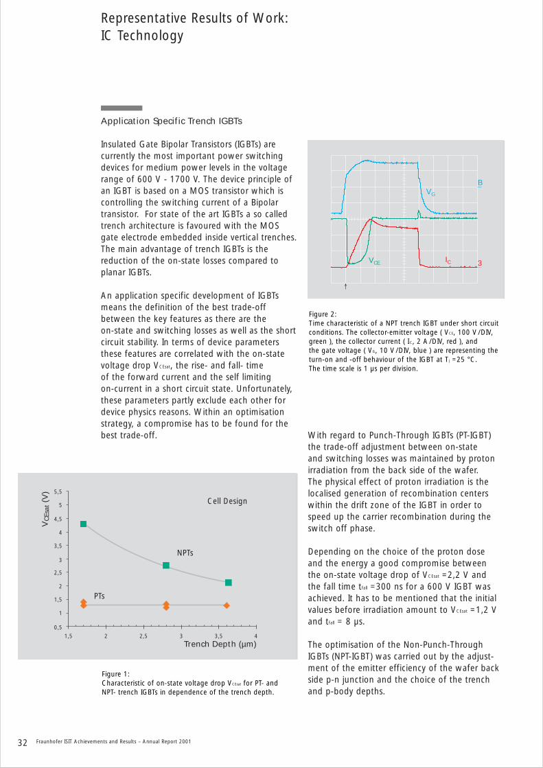
Insulated Gate Bipolar Transistors (IGBTs) are currently the most important power switchingdevices for medium power levels in the voltagerange of 600 V - 1700 V. The device principle ofan IGBT is based on a MOS transistor which iscontrolling the switching current of a Bipolartransistor. For state of the art IGBTs a so calledtrench architecture is favoured with the MOSgate electrode embedded inside vertical trenches.The main advantage of trench IGBTs is the reduction of the on-state losses compared to planar IGBTs.
An application specific development of IGBTsmeans the definition of the best trade-off between the key features as there are the on-state and switching losses as well as the shortcircuit stability. In terms of device parametersthese features are correlated with the on-statevoltage drop VCEsat, the rise- and fall- time of the forward current and the self limiting on-current in a short circuit state. Unfortunately,these parameters partly exclude each other fordevice physics reasons. Within an optimisationstrategy, a compromise has to be found for thebest trade-off. With regard to Punch-Through IGBTs (PT-IGBT)
the trade-off adjustment between on-state and switching losses was maintained by protonirradiation from the back side of the wafer. The physical effect of proton irradiation is thelocalised generation of recombination centerswithin the drift zone of the IGBT in order tospeed up the carrier recombination during theswitch off phase.
Depending on the choice of the proton dose and the energy a good compromise between the on-state voltage drop of VCEsat =2,2 V and the fall time tfall =300 ns for a 600 V IGBT wasachieved. It has to be mentioned that the initialvalues before irradiation amount to VCEsat =1,2 Vand tfall = 8 µs.
The optimisation of the Non-Punch-ThroughIGBTs (NPT-IGBT) was carried out by the adjust-ment of the emitter efficiency of the wafer backside p-n junction and the choice of the trenchand p-body depths.
Representative Results of Work:IC Technology
Trench Depth (µm)1,5 2 2,5 3 3,5 4
Cell Design
NPTs
0,5
1
1,5
2
2,5
3
3,5
4
4,5
5
5,5
VC
Esat
(V)
PTs
Figure 1: Characteristic of on-state voltage drop VCEsat for PT- and NPT- trench IGBTs in dependence of the trench depth.
3
B
VCE IC
VG
Figure 2: Time characteristic of a NPT trench IGBT under short circuitconditions. The collector-emitter voltage ( VCE, 100 V /DIV,green ), the collector current ( I C, 2 A /DIV, red ), and the gate voltage ( VG, 10 V /DIV, blue ) are representing the turn-on and -off behaviour of the IGBT at Tj =25 °C. The time scale is 1 µs per division.
Fraunhofer ISIT Achievements and Results – Annual Report 2001 33
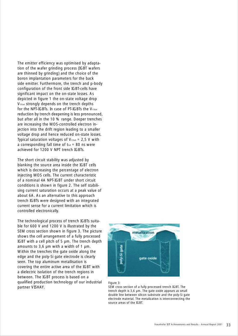
Figure 3: SEM cross section of a fully processed trench IGBT. Thetrench depth is 3,6 µm. The gate oxide appears as smalldouble line between silicon substrate and the poly-Si gateelectrode material. The metalization is interconnecting thesource areas of the IGBT.
The emitter efficiency was optimised by adapta-tion of the wafer grinding process (IGBT wafersare thinned by grinding) and the choice of theboron implantation parameters for the back side emitter. Furthermore, the trench and p-bodyconfiguration of the front side IGBT-cells havesignificant impact on the on-state losses. Asdepicted in figure 1 the on-state voltage dropVCEsat strongly depends on the trench depths for the NPT-IGBTs. In case of PT-IGBTs the VCEsat
reduction by trench deepening is less pronounced,but after all in the 10 % range. Deeper trenchesare increasing the MOS-controlled electron in-jection into the drift region leading to a smallervoltage drop and hence reduced on-state losses. Typical saturation voltages of VCEsat = 2,5 V with a corresponding fall time of tfall = 80 ns wereachieved for 1200 V NPT trench IGBTs.
The short circuit stability was adjusted by blanking the source area inside the IGBT cellswhich is decreasing the percentage of electroninjecting MOS cells. The current characteristic of a nominal 4A NPT-IGBT under short circuitconditions is shown in figure 2. The self stabili-sing current saturation occurs at a peak value ofabout 6A. As an alternative to this approachtrench IGBTs were designed with an integratedcurrent sense for a current limitation which iscontrolled electronically.
The technological process of trench IGBTs suita-ble for 600 V and 1200 V is illustrated by theSEM cross section shown in figure 3. The pictureshows the cell arrangement of a fully processedIGBT with a cell pitch of 5 µm. The trench depthamounts to 3,6 µm with a width of 1 µm.Within the trenches the gate oxide along theedge and the poly-Si gate electrode is clearlyseen. The top aluminum metallisation is covering the entire active area of the IGBT witha dielectric isolation of the trench regions in between. The IGBT process is based on a qualified production technology of our industrialpartner VISHAY.
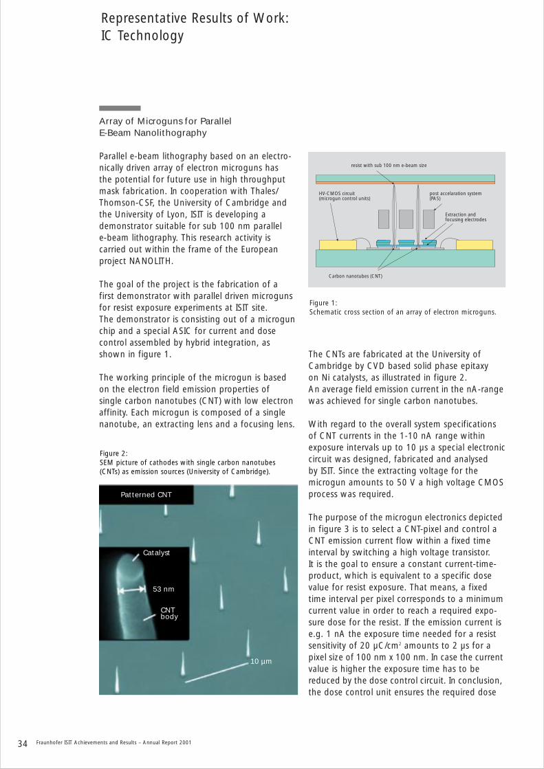
Figure 1: Schematic cross section of an array of electron microguns.
34 Fraunhofer ISIT Achievements and Results – Annual Report 2001
Array of Microguns for Parallel E-Beam Nanolithography
Parallel e-beam lithography based on an electro-nically driven array of electron microguns has the potential for future use in high throughputmask fabrication. In cooperation with Thales/Thomson-CSF, the University of Cambridge andthe University of Lyon, ISIT is developing ademonstrator suitable for sub 100 nm parallel e-beam lithography. This research activity is carried out within the frame of the Europeanproject NANOLITH.
The goal of the project is the fabrication of a first demonstrator with parallel driven microgunsfor resist exposure experiments at ISIT site. The demonstrator is consisting out of a microgunchip and a special ASIC for current and dosecontrol assembled by hybrid integration, asshown in figure 1.
The working principle of the microgun is basedon the electron field emission properties of single carbon nanotubes (CNT) with low electronaffinity. Each microgun is composed of a singlenanotube, an extracting lens and a focusing lens.
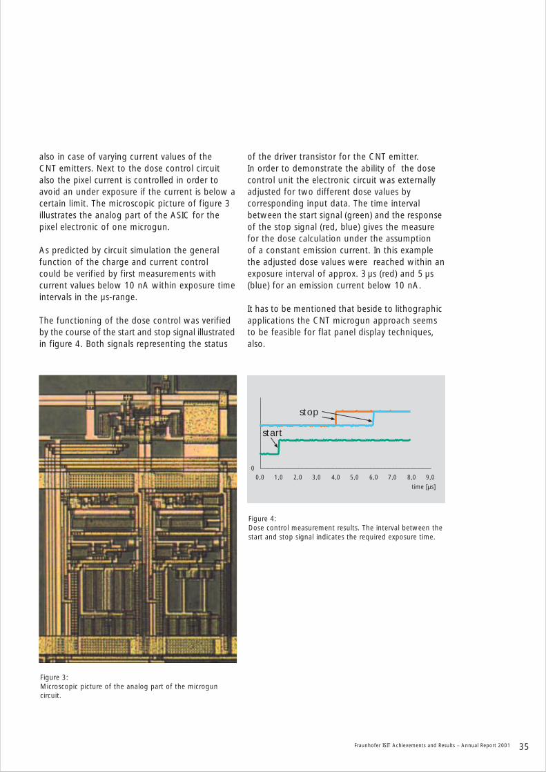
The CNTs are fabricated at the University ofCambridge by CVD based solid phase epitaxy on Ni catalysts, as illustrated in figure 2. An average field emission current in the nA-rangewas achieved for single carbon nanotubes.
With regard to the overall system specificationsof CNT currents in the 1-10 nA range withinexposure intervals up to 10 µs a special electroniccircuit was designed, fabricated and analysed by ISIT. Since the extracting voltage for themicrogun amounts to 50 V a high voltage CMOSprocess was required.
The purpose of the microgun electronics depictedin figure 3 is to select a CNT-pixel and control aCNT emission current flow within a fixed timeinterval by switching a high voltage transistor. It is the goal to ensure a constant current-time-product, which is equivalent to a specific dosevalue for resist exposure. That means, a fixedtime interval per pixel corresponds to a minimumcurrent value in order to reach a required expo-sure dose for the resist. If the emission current ise.g. 1 nA the exposure time needed for a resistsensitivity of 20 µC/cm2 amounts to 2 µs for apixel size of 100 nm x 100 nm. In case the currentvalue is higher the exposure time has to be reduced by the dose control circuit. In conclusion,the dose control unit ensures the required dose
Representative Results of Work:IC Technology
resist with sub 100 nm e-beam size
post accelaration system(PAS)
Extraction andfocusing electrodes
HV-CMOS circuit(microgun control units)
Carbon nanotubes (CNT)
Patterned CNT
Catalyst
53 nm
CNTbody
10 µm
Figure 2: SEM picture of cathodes with single carbon nanotubes(CNTs) as emission sources (University of Cambridge).
also in case of varying current values of the CNT emitters. Next to the dose control circuitalso the pixel current is controlled in order toavoid an under exposure if the current is below acertain limit. The microscopic picture of figure 3illustrates the analog part of the ASIC for thepixel electronic of one microgun.
As predicted by circuit simulation the generalfunction of the charge and current control could be verified by first measurements with current values below 10 nA within exposure timeintervals in the µs-range.
The functioning of the dose control was verifiedby the course of the start and stop signal illustratedin figure 4. Both signals representing the status
Figure 4: Dose control measurement results. The interval between thestart and stop signal indicates the required exposure time.
Figure 3: Microscopic picture of the analog part of the microgun circuit.
Fraunhofer ISIT Achievements and Results – Annual Report 2001 35
of the driver transistor for the CNT emitter. In order to demonstrate the ability of the dosecontrol unit the electronic circuit was externallyadjusted for two different dose values by corresponding input data. The time interval between the start signal (green) and the responseof the stop signal (red, blue) gives the measurefor the dose calculation under the assumption of a constant emission current. In this examplethe adjusted dose values were reached within anexposure interval of approx. 3 µs (red) and 5 µs(blue) for an emission current below 10 nA.
It has to be mentioned that beside to lithographicapplications the CNT microgun approach seemsto be feasible for flat panel display techniques,also.
00,0 1,0 2,0 3,0 4,0 5,0 6,0 7,0 8,0 9,0
time [µs]
stop
start
36 Fraunhofer ISIT Achievements and Results – Annual Report 2001
Optical MEMS Switches forTelecommunication Networks
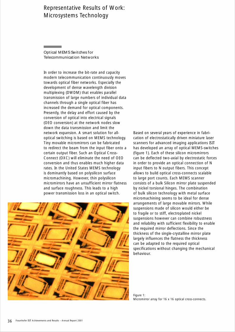
In order to increase the bit-rate and capacitymodern telecommunication continuously movestowards optical fiber networks. Especially thedevelopment of dense wavelength division multiplexing (DWDM) that enables parallel transmission of large numbers of individual datachannels through a single optical fiber has increased the demand for optical components.Presently, the delay and effort caused by the conversion of optical into electrical signals (OEO conversion) at the network nodes slowdown the data transmission and limit the network expansion. A smart solution for all-optical switching is based on MEMS technology.Tiny movable micromirrors can be fabricated to redirect the beam from the input fiber onto acertain output fiber. Such an Optical Cross-Connect (OXC) will eliminate the need of OEOconversion and thus enables much higher datarates. In the United States MEMS technology is dominantly based on polysilicon surface micromachining. However, thin polysiliconmicromirrors have an unsufficient mirror flatnessand surface roughness. This leads to a highpower transmission loss in an optical switch.
Based on several years of experience in fabri-cation of electrostatically driven miniature laserscanners for advanced imaging applications ISIThas developed an array of optical MEMS-switches(figure 1). Each of these silicon micromirrors can be deflected two-axial by electrostatic forcesin order to provide an optical connection of Ninput fibers to N output fibers. This conceptallows to build optical cross-connects scalable to large port counts. Each MEMS scanner consists of a bulk Silicon mirror plate suspendedby nickel torsional hinges. The combination of bulk silicon technology with metal surfacemicromachining seems to be ideal for densearrangements of large movable mirrors. Whilesuspensions made of silicon would either be to fragile or to stiff, electroplated nickel suspensions however can combine robustnessand reliability with sufficient flexibility to enablethe required mirror deflections. Since the thickness of the single-crystalline mirror plate largely influences the flatness the thickness can be adapted to the required optical specifications without changing the mechanicalbehaviour.
Representative Results of Work:Microsystems Technology
Figure 1: Micromirror array for 16 x 16 optical cross-connects.
Fraunhofer ISIT Achievements and Results – Annual Report 2001 37
MP-CC: A Competence Cluster for Silicon and Polymer Micro System Technology inSchleswig-Holstein/Germany
The “Micro Plastics – Competence Cluster” (MP-CC) integrates in unique way the knowledgeand technological skills of fine mechanics, plastics engineering and silicon technology inSchleswig-Holstein. On the one hand, the projectpartners act as a technology and service providerfor customer specific products. On the otherhand, the joint network develops and prototypeshigh tech products for MST applications likemicro lenses, diffractive optical elements (DOEs)or fluidic channel structures.
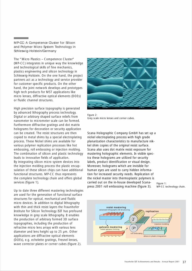
High precision surface topography is generatedby advanced lithography process technology.Digital or arbitrary shaped surface reliefs fromnanometer to micrometer scale can be formed.Furthermore diffractive gratings and dot matrixholograms for decoration or security applicationcan be created. The resist structures are thencopied to metal shims by a special electroplatingprocess. These Nickel shims are available forvarious polymer replication processes like hotembossing, roll embossing or injection molding.The combination of silicon and plastic technologyleads to innovative fields of application. By integrating silicon micro system devices intothe injection molding process the plastic encap-sulation of these silicon chips can have additionalfunctional structures. MP-CC thus represents the complete technology chain and offers globalservices (figure 1).
Up to date three different mastering technologiesare used for the generation of functional surfacestructures for optical, mechanical and fluidicmicro devices. In addition to digital lithographywith thin and thick resist layers the FraunhoferInstitute for Silicon Technology ISIT has profoundknowledge in grey scale lithography. It enablesthe production of arbitrary formed 3D surface topographies, including the production of refractive micro lens arrays with various lens diameter and lens height up to 25 µm. Otherapplications are diffractive optical elements(DOEs), e.g. echelette gratings, Fresnel lenses,wave corrector plates or corner cubes (figure 2).
replication
silicon-in plastic integration
roll embossing
injection molding
nickel galvano forming
advanced lithographic 3D structuring
galvano mastering
resist mastering
Figure 2: Grey scale micro lenses and corner cubes.
Figure 1: MP-CC technology chain.
Scana Holographic Company GmbH has set up anickel electroplating process with high gradeplanarization characteristics to manufacture nik-kel shim copies of the original resist surface.Scana also uses dot matrix resist exposure formastering holographic elements. In visible spec-tra these holograms are utilized for securitylabels, product identification or visual design.Moreover, holograms which are invisible forhuman eyes are used to carry hidden informa-tion for increased security needs. Replication ofthe nickel master into thermoplastic polymers iscarried out on the in-house developed Scana-press 2001 roll embossing machine (figure 3).
38 Fraunhofer ISIT Achievements and Results – Annual Report 2001
For higher aspect ratios, replication by hot injection molding process is preferred. The corecompetence of Kuhnke GmbH is injection molding for various applications like electricalrelays or pneumatic valves. The high volumemanufacturing of plastic precision components isbased on fine mechanics for molding tool construction and excellent micro injection processcontrol. Besides the replication of 3D surfaces a key technology will be the integration ofSilicon MEMS devices in polymer encapsulationwithin the injection molding process. In additionthe molded plastic housing can contain functional geometrical elements. Examples aremicro channels or armature shafts.
As a potential application partner Basler VisionTechnologies takes over the role of prototypingoptical elements and systems. The costs of automated optical quality control like compactdisc inspection or web inspection (paper, textileor rolled steel production) can be lowered substantially through the use of high qualitypolymer optics.
The IZET Innovationszentrum Itzehoe completesthe scope of the competence cluster by providing marketing and market analysis skills and knowledge. The website www.mp-cc.de integrates the marketing efforts of MP-CC products and services and acts as a common data base.
The interaction between the particular techno-logy processes is ensured by internal standardinterface geometries. Fast prototyping of new geometry designs is offered. MP-CC servicesare open to any potential customer and reachesfrom advisory consultation up to full customeradapted production.
Representative Results of Work:Microsystems Technology
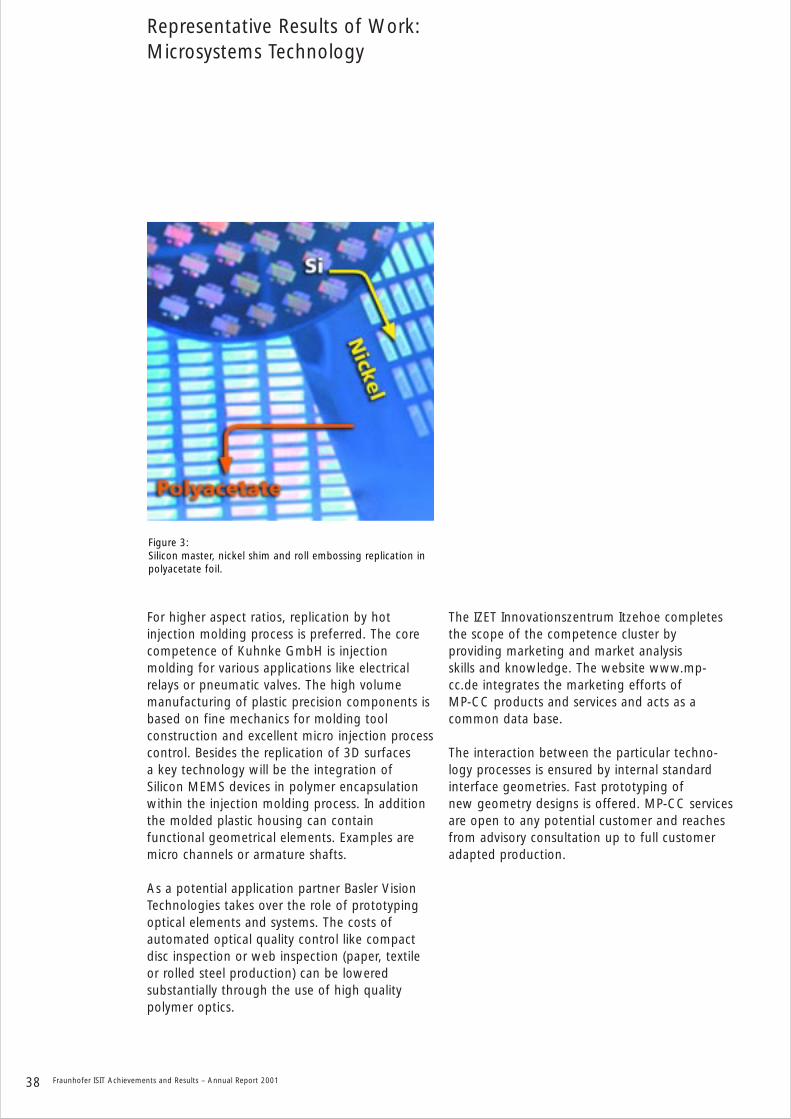
Figure 3: Silicon master, nickel shim and roll embossing replication inpolyacetate foil.
Fraunhofer ISIT Achievements and Results – Annual Report 2001 39
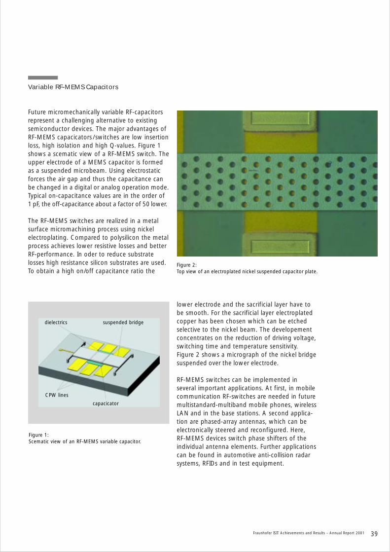
Variable RF-MEMS Capacitors
Future micromechanically variable RF-capacitorsrepresent a challenging alternative to existingsemiconductor devices. The major advantages ofRF-MEMS capacicators / switches are low insertionloss, high isolation and high Q-values. Figure 1shows a scematic view of a RF-MEMS switch. Theupper electrode of a MEMS capacitor is formedas a suspended microbeam. Using electrostaticforces the air gap and thus the capacitance canbe changed in a digital or analog operation mode.Typical on-capacitance values are in the order of1 pF, the off-capacitance about a factor of 50 lower.
The RF-MEMS switches are realized in a metalsurface micromachining process using nickel electroplating. Compared to polysilicon the metalprocess achieves lower resistive losses and betterRF-performance. In oder to reduce substrate losses high resistance silicon substrates are used.To obtain a high on/off capacitance ratio the
lower electrode and the sacrificial layer have tobe smooth. For the sacrificial layer electroplatedcopper has been chosen which can be etchedselective to the nickel beam. The developementconcentrates on the reduction of driving voltage,switching time and temperature sensitivity. Figure 2 shows a micrograph of the nickel bridgesuspended over the lower electrode.
RF-MEMS switches can be implemented in several important applications. At first, in mobilecommunication RF-switches are needed in futuremultistandard-multiband mobile phones, wirelessLAN and in the base stations. A second applica-tion are phased-array antennas, which can be electronically steered and reconfigured. Here, RF-MEMS devices switch phase shifters of theindividual antenna elements. Further applicationscan be found in automotive anti-collision radarsystems, RFIDs and in test equipment.
Figure 1: Scematic view of an RF-MEMS variable capacitor.
Figure 2: Top view of an electroplated nickel suspended capacitor plate.
dielectrics suspended bridge
CPW lines
capacicator
40 Fraunhofer ISIT Achievements and Results – Annual Report 2001
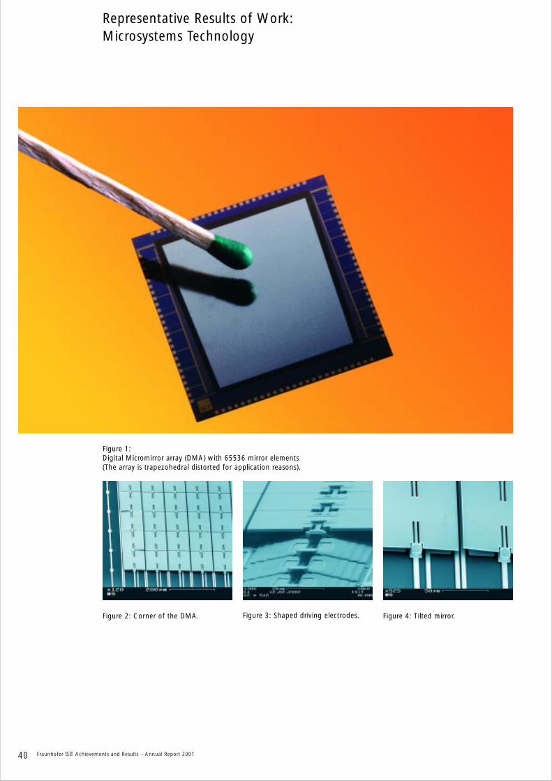
Figure 1: Digital Micromirror array (DMA) with 65536 mirror elements (The array is trapezohedral distorted for application reasons).
Figure 2: Corner of the DMA. Figure 4: Tilted mirror.Figure 3: Shaped driving electrodes.
Representative Results of Work:Microsystems Technology
Fraunhofer ISIT Achievements and Results – Annual Report 2001 41
Digital Micromirror Arrays for Optical Switching
Fraunhofer ISIT is active in the field of digitalmicromirror arrays (DMA) for more than sevenyears. Optimizing our metal surface micro-machining technology we are able to fabricateDMAs with 420 mm2 array area and 65536 elements with optical surface quality (figure 1+2).
DMAs are becoming a key component for a new class of digital devices, such as projectiondisplays, imaging systems and printing systems.Especially in telecommunication optical switchingis an important feature. Selection free connectionof optical fiber bundles e.g. in telephone centraloffices is one of the main application.
The actual process flow allows a wide range of parameter variation. A single mirror line with afew tenth of elements is just possible as an arrayof 256 x 256 elements. The mirrorplate sizecould vary from 50 µm x 50 µm to 150 µm x 150µm (more details see table 1). Our 3D electro-plating enables us to integrate wedge shapedelectrodes (figure 3) to reduce the address voltage for the electrostatic mirror actuation.
Chip size: Up to 30 mm x 30 mmMirror edgelength: 50 µm to 150 µmMirror array size: Up to 256 x 256 elem.Tilting angle: Up to ± 15° (mech.)Resonant frequency: Up to 25 kHzSwitching speed About 50 µsMirrorplate flatness: < 120 nmDriving voltage: 160 V (typical value)
60 V (biassing mode)Monolithical integration on address circuit: Feasible
Figure 5: White light interferometer plot of100 µm mirror plate flatness.
Table 1: Typical parameters for DMAs at Fraunhofer ISIT.
A good CD control reduces the mirror spacing toless than 2 µm (figure 4). The stress optimizedelectroplating process for the mirrorplate resultsin flatness values smaller than 120 nm (figure 5).Because of the low process temperatures duringthe metal surface micro-machining processmonolithical integration of the mirrorarray on apreprocessed wafer with the mirror address circuits fabricated in BCD technology is feasible.
42 Fraunhofer ISIT Achievements and Results – Annual Report 2001
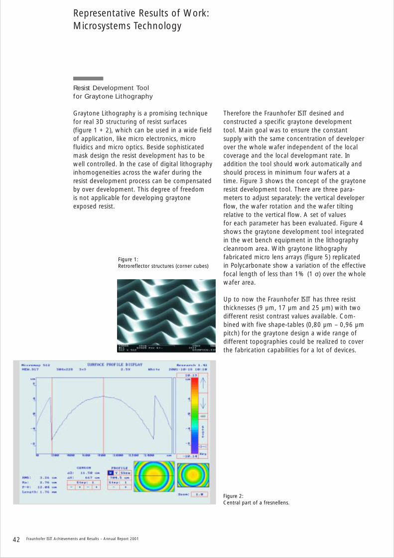
Resist Development Tool for Graytone Lithography
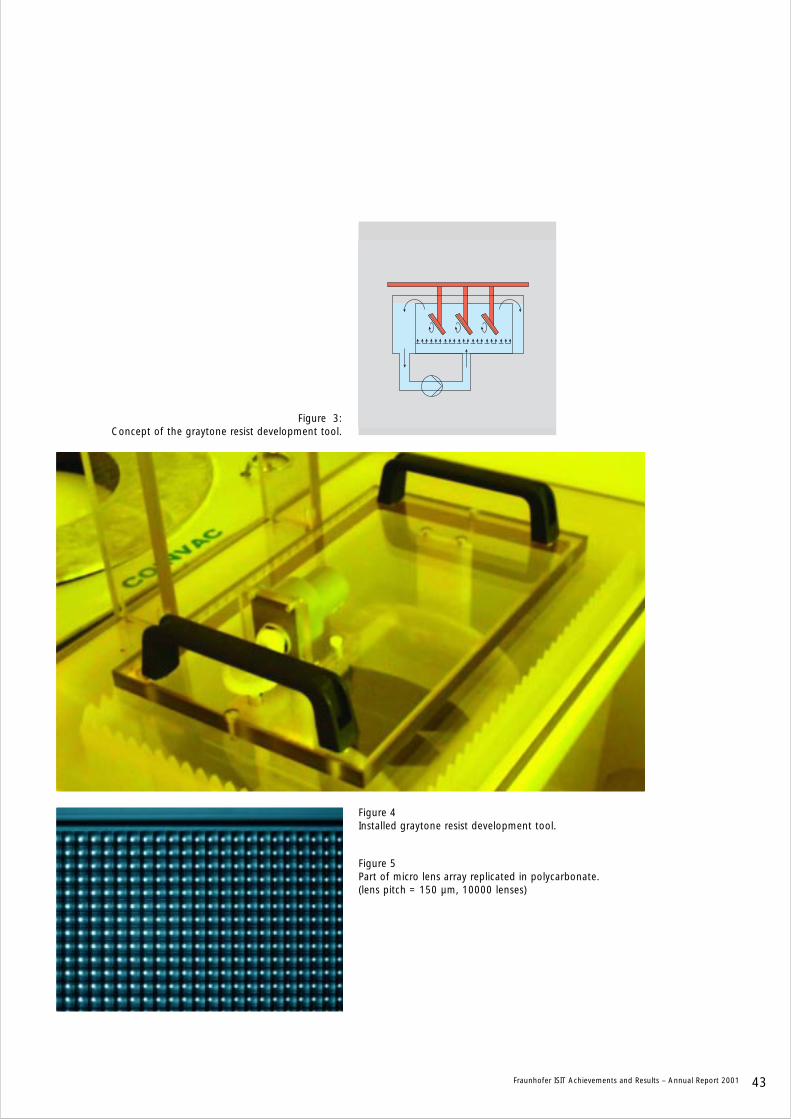
Graytone Lithography is a promising techniquefor real 3D structuring of resist surfaces (figure 1 + 2), which can be used in a wide fieldof application, like micro electronics, micro fluidics and micro optics. Beside sophisticatedmask design the resist development has to bewell controlled. In the case of digital lithographyinhomogeneities across the wafer during theresist development process can be compensatedby over development. This degree of freedom is not applicable for developing graytone exposed resist.
Therefore the Fraunhofer ISIT desined and constructed a specific graytone developmenttool. Main goal was to ensure the constant supply with the same concentration of developerover the whole wafer independent of the localcoverage and the local developmant rate. Inaddition the tool should work automatically andshould process in minimum four wafers at atime. Figure 3 shows the concept of the graytoneresist development tool. There are three para-meters to adjust separately: the vertical developerflow, the wafer rotation and the wafer tiltingrelative to the vertical flow. A set of values for each parameter has been evaluated. Figure 4shows the graytone development tool integratedin the wet bench equipment in the lithographycleanroom area. With graytone lithography fabricated micro lens arrays (figure 5) replicatedin Polycarbonate show a variation of the effectivefocal length of less than 1% (1 σ) over the wholewafer area.
Up to now the Fraunhofer ISIT has three resistthicknesses (9 µm, 17 µm and 25 µm) with twodifferent resist contrast values available. Com-bined with five shape-tables (0,80 µm – 0,96 µmpitch) for the graytone design a wide range ofdifferent topographies could be realized to coverthe fabrication capabilities for a lot of devices.
Representative Results of Work:Microsystems Technology
Figure 1: Retroreflector structures (corner cubes)
Figure 2:Central part of a fresnellens.
Fraunhofer ISIT Achievements and Results – Annual Report 2001 43
Figure 3: Concept of the graytone resist development tool.
Figure 5Part of micro lens array replicated in polycarbonate. (lens pitch = 150 µm, 10000 lenses)
Figure 4Installed graytone resist development tool.
44 Fraunhofer ISIT Achievements and Results – Annual Report 2001
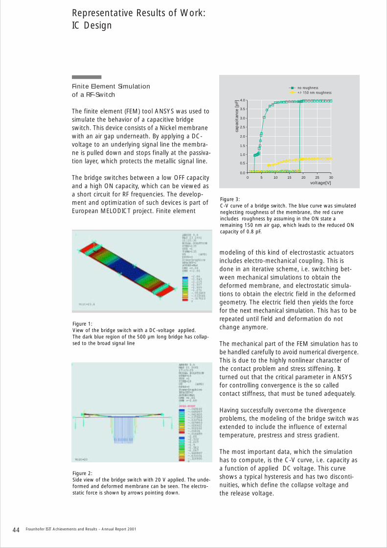
Finite Element Simulation of a RF-Switch
The finite element (FEM) tool ANSYS was used tosimulate the behavior of a capacitive bridgeswitch. This device consists of a Nickel membranewith an air gap underneath. By applying a DC-voltage to an underlying signal line the membra-ne is pulled down and stops finally at the passiva-tion layer, which protects the metallic signal line.
The bridge switches between a low OFF capacityand a high ON capacity, which can be viewed asa short circuit for RF frequencies. The develop-ment and optimization of such devices is part ofEuropean MELODICT project. Finite element
modeling of this kind of electrostastic actuatorsincludes electro-mechanical coupling. This isdone in an iterative scheme, i.e. switching bet-ween mechanical simulations to obtain thedeformed membrane, and electrostatic simula-tions to obtain the electric field in the deformedgeometry. The electric field then yields the forcefor the next mechanical simulation. This has to berepeated until field and deformation do notchange anymore.
The mechanical part of the FEM simulation has tobe handled carefully to avoid numerical divergence.This is due to the highly nonlinear character ofthe contact problem and stress stiffening. It turned out that the critical parameter in ANSYSfor controlling convergence is the so called contact stiffness, that must be tuned adequately.
Having successfully overcome the divergence problems, the modeling of the bridge switch wasextended to include the influence of externaltemperature, prestress and stress gradient.
The most important data, which the simulationhas to compute, is the C-V curve, i.e. capacity asa function of applied DC voltage. This curveshows a typical hysteresis and has two disconti-nuities, which define the collapse voltage andthe release voltage.
Representative Results of Work:IC Design
0 5 10 15 20
voltage[V]
3.0
cap
acit
ance
[p
F]
2.5
2.0
1.5
1.0
0.5
0.0
3.5
4.0
25 30
no roughness+/- 150 nm roughness
Figure 1:View of the bridge switch with a DC-voltage applied.The dark blue region of the 500 µm long bridge has collap-sed to the broad signal line
Figure 2: Side view of the bridge switch with 20 V applied. The unde-formed and deformed membrane can be seen. The electro-static force is shown by arrows pointing down.
Figure 3:C-V curve of a bridge switch. The blue curve was simulatedneglecting roughness of the membrane, the red curve includes roughness by assuming in the ON state a remaining 150 nm air gap, which leads to the reduced ONcapacity of 0.8 pF.
Fraunhofer ISIT Achievements and Results – Annual Report 2001 45
Development of Designkits for TechnologyDependent Accelerated Chipfinishing
With the ability to process an increasing amount ofdesigns in an increasing number of different tech-nologies the need for accelerated chipfinishing pro-cedures has arised to speed up the time from thefinished product design to final mask design. Theaim is it to take the single product design, made byISIT or the customer himself, and to generate acost and place optimised final mask design. Toreduce errors the procedure is fully automised andintegrated in the design environment of CADENCE,the IC-design-software that is used.
FhG-ISIT Customers
Designs
Technology A
Technology B
Technology C Designkit • Litho Mark Generator • Reticle Array Optimizer • Final Mask Placement
Submission to Mask-Shop
Figure 1: Design flow.
Figure 2: Cross-Section window.
Figure 3: Stepping array optimisation basedon generic algorithms.
Generator for Lithography and Monitoring StructuresTo introduce new technologies an important taskis the generation of a set of process dependendstructures for alignment and monitoring. This setcan be generated automatically and the resultcan be checked by the integrated cross-sectionviewer. It is actually planned to integrate anadditional direct interface to fab control systemsto control the direct effect of process modifica-tions on the given structures.
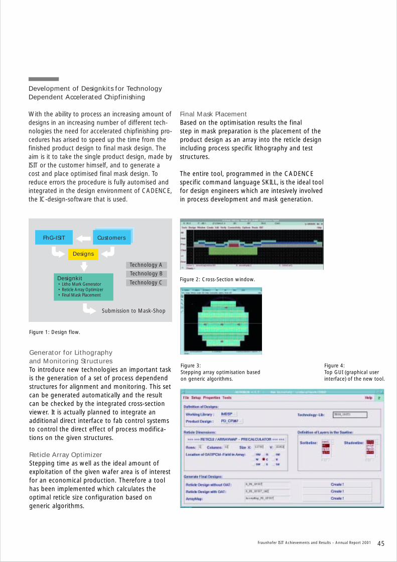
Reticle Array OptimizerStepping time as well as the ideal amount ofexploitation of the given wafer area is of interestfor an economical production. Therefore a toolhas been implemented which calculates the optimal reticle size configuration based on generic algorithms.
Figure 4: Top GUI (graphical user interface) of the new tool.
Final Mask PlacementBased on the optimisation results the final step in mask preparation is the placement of theproduct design as an array into the reticle designincluding process specific lithography and teststructures.
The entire tool, programmed in the CADENCEspecific command language SKILL, is the ideal toolfor design engineers which are intesively involvedin process development and mask generation.
46 Fraunhofer ISIT Achievements and Results – Annual Report 2001
fluidic control waste data transmissionenvironmental
sample
samplepreparation
electricalbiochip
evaluationelectronics
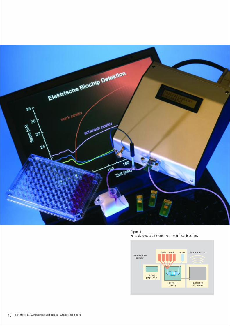
Figure 1:Portable detection system with electrical biochips.

Fraunhofer ISIT Achievements and Results – Annual Report 2001 47
Bio-MST Study “Detection of biological weapons”
“The threat potentials posed by biologicalweapons are largely underestimated by theGerman politics as well as by the German public.”
This is the first sentence of a study published in July 2001 bearing the subtitle “defence strategies from the viewpoint of new micro-system and biochip technologies.”
The approximately 90-pages study reviewing the detection of biological weapons was compiledby Anton Heuberger and Rainer Hintsche on behalf of the federal ministry of defence and published by the Fraunhofer Institute ofscientific-technical trend analysis (INT), more than3 month before the tragic attacks have happenedin the USA. Due to the anthrax attacks in theUSA the statements in the study proved to be very close to reality and gained great interestin the public.
The study shows the immense threat potentialposed by the use of different biological weapons.It brings to attention the often much higher toxicity of such substances compared to chemicalsand the relatively easy availability. In the closingwords it warns explicitly of the danger of attacksby terrorist organisations. “Due to the fact thatwe are living in a time of great politic stabilitythe need for action results primarily due to thethreat posed by terrorism including state terrorismby rouges countries. It would be fatal to waitwith preventive measures until the first worst casehas happened.“
The analysis of existing and utilised systems forthe defence of biological weapons reveals a limitation towards classical decentralised labsystems, except a few very conventional andinsufficient systems in the USA. The immediateset-up of a rapid to be activated and possiblearea-wide detection system for the protection ofthe civil population is strongly recommended.Here the application of electrical biochip technology, developed at ISIT in the department“biotechnical microsystems” in combination with a microfluidic module is an option.
The application of an autonomous detectionsystem automatically taking environmental samples (water, air) and testing them for severalbiological hazardous substances was evaluated.The results of the tests are transmitted to a central control station. The core of the detectionsystem consists of electrical biochips and anti-body-coated particles. In initial feasibility studiessuch a system proved the suitability for a highlysensitive and specific detection of environmentaltoxins.
Even the detection of picomolar concentrationsof proteins like toxins was proven. This very low detection limit is suitable for the detection of the most toxic biological weapon known to mankind, the botulinus toxin (0.1 µg are lethal for an average human). With a total of 5 death victims the USA had to learn howinsufficient they are prepared for such attacksand as a result remarkably increased the financial support for the development of protective systems. It is to be hoped that therehas not to be a first tragic case in Germany before it will act in a similar way.
Source: Anton Heuberger und Rainer Hintsche,“Detektion biologischer Kampfstoffe – Abwehr-strategien unter dem Gesichtspunkt neuerMikrosystem- und Biochiptechnologien”, Erstellt im Auftrag des Bundesministeriums derVerteidigung, Herausgegeben vom FraunhoferInstitut für Naturwissenschaftlich-TechnischeTrendanalysen (INT), Juli 2001.
Representative Results of Work:Biotechnical Microsystems
Figure 2: Scheme of a bioweapons detector.
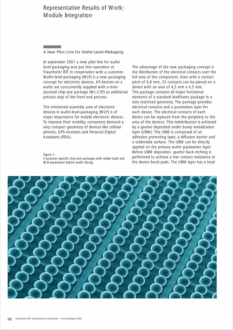
48 Fraunhofer ISIT Achievements and Results – Annual Report 2001
A New Pilot Line for Wafer-Level-Packaging
In september 2001 a new pilot line for waferlevel packaging was put into operation atFraunhofer ISIT in cooperation with a customer.Wafer-level-packaging (WLP) is a new packagingconcept for electronic devices. All devices on awafer are concurrently supplied with a mini-aturized chip-size package (WL-CSP) as additionalprocess step of the front end process.
The minimized assembly area of electronic devices in wafer-level-packaging (WLP) is ofmajor importance for mobile electronic devices.To improve their mobility, consumers demand avery compact geometry of devices like cellularphones, GPS-receivers and Personal DigitalAssistants (PDA).
The advantage of the new packaging concept isthe distribution of the electrical contacts over thefull area of the component. Even with a contactpitch of 0,8 mm, 25 contacts can be placed on adevice with an area of 4,5 mm x 4,5 mm.This package contains all major functional elements of a standard leadframe package in avery restricted geometry. The package provideselectrical contacts and a passivation layer foreach device. The electrical contacts of each device can be replaced from the periphery to thearea of the devices. This redistribution is achievedby a sputter deposited under bump metalizationlayer (UBM). The UBM is composed of an adhesion promoting layer, a diffusion barrier anda solderable surface. The UBM can be directlyapplied on the primary wafer passivation layer.Before UBM depositon, sputter back etching isperformed to achieve a low contact resistance tothe device bond pads. The UBM layer has a total
Representative Results of Work:Module Integration
Figure 1: Crustomer specific chip-size packages with solder balls andBCB passivation before wafer dicing.
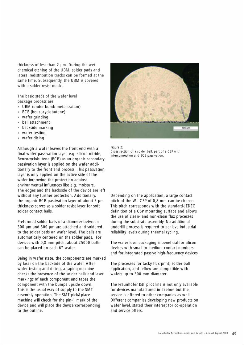
Fraunhofer ISIT Achievements and Results – Annual Report 2001 49
thickness of less than 2 µm. During the wet chemical etching of the UBM, solder pads andlateral redistribution tracks can be formed at thesame time. Subsequently, the UBM is coveredwith a solder resist mask.
The basic steps of the wafer level package process are:• UBM (under bumb metallization)• BCB (benzocyclobutene)• wafer grinding• ball attachment• backside marking• wafer testing• wafer dicing
Although a wafer leaves the front end with afinal wafer passivation layer, e.g. silicon nitride,Benzocyclobutene (BCB) as an organic secondarypassivation layer is applied on the wafer addi-tionally to the front end process. This passivationlayer is only applied on the active side of thewafer improving the protection against environmental influences like e.g. moisture. The edges and the backside of the device are leftwithout any further protection. Additionally, the organic BCB passivation layer of about 5 µmthickness serves as a solder resist layer for softsolder contact balls.
Preformed solder balls of a diameter between300 µm and 500 µm are attached and solderedto the solder pads on wafer level. The balls areautomatically centered on the solder pads. Fordevices with 0,8 mm pitch, about 25000 ballscan be placed on each 6" wafer.
Being in wafer state, the components are markedby laser on the backside of the wafer. After wafer testing and dicing, a taping machinechecks the presence of the solder balls and lasermarkings of each component and tapes the component with the bumps upside down. This is the usual way of supply to the SMTassembly operation. The SMT pick&place machine will check for the pin-1 mark of thedevice and will place the device corresponding to the outline.
Depending on the application, a large contactpitch of the WL-CSP of 0,8 mm can be chosen.This pitch corresponds with the standard-JEDECdefinition of a CSP mounting surface and allowsthe use of clean- and non-clean flux processesduring the substrate assembly. No additionalunderfill process is required to achieve industrialreliability levels during thermal cycling.
The wafer level packaging is beneficial for silicondevices with small to medium contact numbersand for integrated passive high-frequency devices.
The processes for tacky flux print, solder ballapplication, and reflow are compatible withwafers up to 300 mm diameter.
The Fraunhofer ISIT pilot line is not only availablefor devices manufactured in Itzehoe but the service is offered to other companies as well.Different companies developing new products onwafer level, stated their interest for co-operationand service offers.
Figure 2: Cross section of a solder ball, part of a CSP withinterconnection and BCB passivation.
50 Fraunhofer ISIT Achievements and Results – Annual Report 2001
Manufacturing of an Optical Module forUV-Laser Ablation and Polishing the Cornea Surfaces of Human Eyes
ManufacturingUsing UV-Lasers the dream to live without glassesor contact lenses is becoming real. Today wave-front aberrations caused by astigmatism or higher order aberrations can be compensated bya thickness modelling of the outer cornea.
Laser Treatment TechniquesLaser ablation techniques of the human corneahave been continuously improved. Older techniques directly ablated the outer cornea (PRK-treatment) by laser radiation.
The actual Lasik-technique cuts first a 160 µm thincircular flap of the epithel that is bend to one sideand then thins down the cornea by local laserablation to achieve the desired wavefront correc-tion. The flap is then bent back and pressed. By capillary forces, the flap sucks down to the cornea by itself serving as a natural plaster.The treatment of the inner cornea is less painfuland improves and fasten the heal up process.Today, the healing process is performed accordingto scientific directions of the commission for refrac-tive surgery on an area around 6 mm diameter toavoid so called ghost pictures in the dark. Thiseffect is caused when the pupil widens beyondthe laser treated zone. The patient senses a secondview area. According to the directions, a minimumcornea thickness above 250 µm is retained.
The Zyoptix-technique developed by the germancompany Technolas Ophthalmologische SystemeGmbH, a subsidiary of Bausch & Lomb is the furthest developed laser treatment techniquetoday, offering a fast individually designed treatment. It is based on the above mentionedLasik-method with further improvements in themeasurement of physiological eye anomalies,improved laser scan control by fast eye trackingand truncated gaussian laser beam profile withtwo spot sizes to ablate and polish the corneasurface. With this technique, the surgeon is ableto provide an individual treatment to correct thespecific wavefront aberrations of each eye of apatient.
Laser Beam ModificationA special UV-radiation intensity profile was developed by Fraunhofer ISIT and Technolas toachieve smooth transitions between overlappingablation spots on the cornea. In a joint researcheffort, the feasibility for a intensity profiling, radiation hard UV-mask with very low backreflection and indication of use could be demon-strated. The glass chips are manufactured ondouble side polished 150 mm quartz wafer. The demanded truncated gaussian intensity profile could be realised by a special computerbased mask structuring algorithm. Experimentaldevices used chips precision bonded in cavities of chip card-like carriers to ease handling andshipping. During the development phase, different departments became involved rangingfrom mask design, microsystems technologyincluding wafer dicing and inspection operationsup to module integration.
Maturing of a Process FlowTo provide a sufficient number of experimentalchips, Fraunhofer ISIT established a customerspecific production flow with all the requiredquality assessment steps and work organisation.Embedded in a logistics schedule provided byTechnolas, ISIT became one link of a supply-chain. The internal process flow was re-organisedat ISIT to avoid extra work and improve efficiency. A further optimisation was gained from harmo-nising the ISIT process flow with the processes ofthe other suppliers and the customer itself.
The single work-steps became distributed to the site which is best experienced. In this way, a cost efficient, well balanced and supervisedprocess flow could be realised for this precisionexperimental device. Each work step is defined ina work description to provide the base for a later quality audit through Technolas. The operators are trained frequently to secure ahigh state of knowledge.
Each single treatment opening in the chips isinspected before and after dicing to screen out
Representative Results of Work:Module Integration
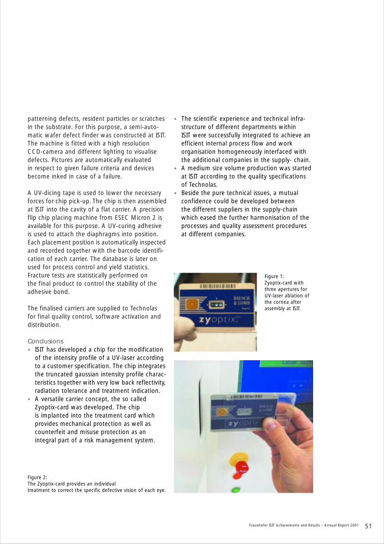
Fraunhofer ISIT Achievements and Results – Annual Report 2001 51
patterning defects, resident particles or scratchesin the substrate. For this purpose, a semi-auto-matic wafer defect finder was constructed at ISIT.The machine is fitted with a high resolutionCCD-camera and different lighting to visualisedefects. Pictures are automatically evaluated in respect to given failure criteria and devicesbecome inked in case of a failure.
A UV-dicing tape is used to lower the necessaryforces for chip pick-up. The chip is then assembledat ISIT into the cavity of a flat carrier. A precisionflip chip placing machine from ESEC Micron 2 isavailable for this purpose. A UV-curing adhesiveis used to attach the diaphragms into position.Each placement position is automatically inspectedand recorded together with the barcode identifi-cation of each carrier. The database is later onused for process control and yield statistics.Fracture tests are statistically performed on the final product to control the stability of theadhesive bond.
The finalised carriers are supplied to Technolasfor final quality control, software activation anddistribution.
Conclusions• ISIT has developed a chip for the modification
of the intensity profile of a UV-laser accordingto a customer specification. The chip integratesthe truncated gaussian intensity profile charac-teristics together with very low back reflectivity,radiation tolerance and treatment indication.
• A versatile carrier concept, the so called Zyoptix-card was developed. The chip is implanted into the treatment card whichprovides mechanical protection as well ascounterfeit and misuse protection as an integral part of a risk management system.
• The scientific experience and technical infra-structure of different departments within ISIT were successfully integrated to achieve anefficient internal process flow and work organisation homogeneously interfaced withthe additional companies in the supply- chain.
• A medium size volume production was startedat ISIT according to the quality specificationsof Technolas.
• Beside the pure technical issues, a mutual confidence could be developed between the different suppliers in the supply-chainwhich eased the further harmonisation of theprocesses and quality assessment proceduresat different companies.
Figure 1: Zyoptix-card withthree apertures forUV-laser ablation ofthe cornea afterassembly at ISIT.
Figure 2: The Zyoptix-card provides an individual treatment to correct the specific defective vision of each eye.
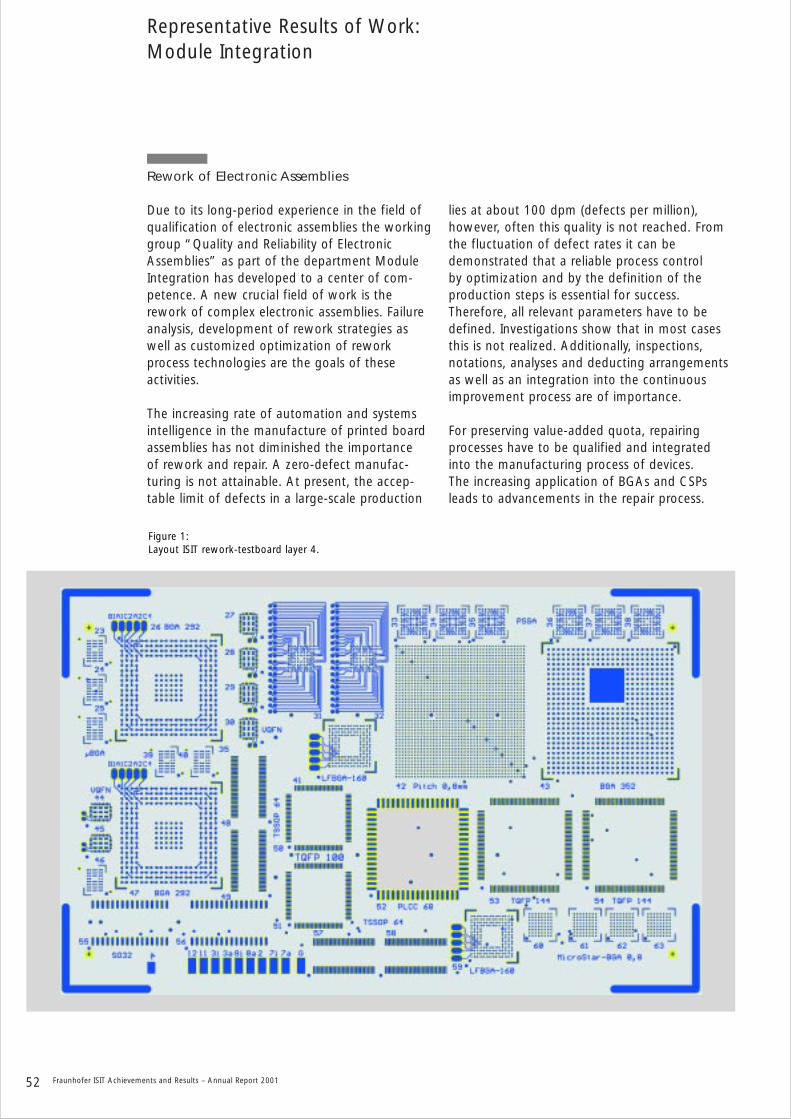
52 Fraunhofer ISIT Achievements and Results – Annual Report 2001
Rework of Electronic Assemblies
Due to its long-period experience in the field ofqualification of electronic assemblies the workinggroup “Quality and Reliability of ElectronicAssemblies” as part of the department ModuleIntegration has developed to a center of com-petence. A new crucial field of work is therework of complex electronic assemblies. Failureanalysis, development of rework strategies aswell as customized optimization of rework process technologies are the goals of these activities.
The increasing rate of automation and systemsintelligence in the manufacture of printed boardassemblies has not diminished the importance of rework and repair. A zero-defect manufac-turing is not attainable. At present, the accep-table limit of defects in a large-scale production
lies at about 100 dpm (defects per million),however, often this quality is not reached. From the fluctuation of defect rates it can be demonstrated that a reliable process control by optimization and by the definition of the production steps is essential for success.Therefore, all relevant parameters have to bedefined. Investigations show that in most casesthis is not realized. Additionally, inspections,notations, analyses and deducting arrangementsas well as an integration into the continuousimprovement process are of importance.
For preserving value-added quota, repairing processes have to be qualified and integratedinto the manufacturing process of devices. The increasing application of BGAs and CSPsleads to advancements in the repair process.
Representative Results of Work:Module Integration
Figure 1: Layout ISIT rework-testboard layer 4.
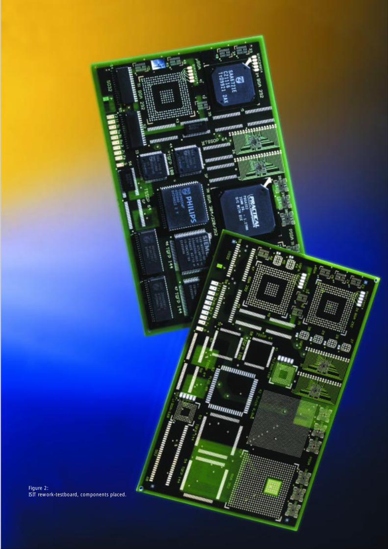
Figure 2: ISIT rework-testboard, components placed.
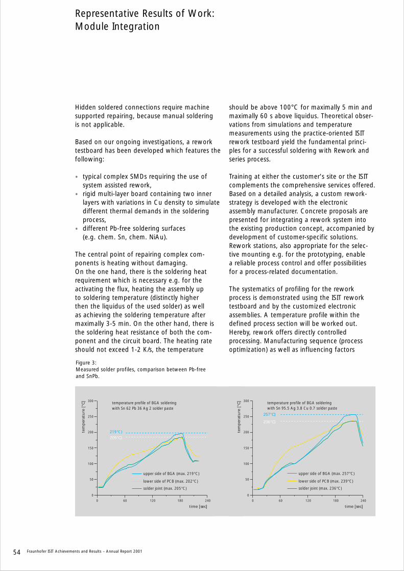
54 Fraunhofer ISIT Achievements and Results – Annual Report 2001
Hidden soldered connections require machinesupported repairing, because manual soldering is not applicable.
Based on our ongoing investigations, a reworktestboard has been developed which features thefollowing:
• typical complex SMDs requiring the use ofsystem assisted rework,
• rigid multi-layer board containing two innerlayers with variations in Cu density to simulatedifferent thermal demands in the solderingprocess,
• different Pb-free soldering surfaces (e.g. chem. Sn, chem. NiAu).
The central point of repairing complex com-ponents is heating without damaging. On the one hand, there is the soldering heatrequirement which is necessary e.g. for the activating the flux, heating the assembly up to soldering temperature (distinctly higher then the liquidus of the used solder) as well as achieving the soldering temperature aftermaximally 3-5 min. On the other hand, there isthe soldering heat resistance of both the com-ponent and the circuit board. The heating rateshould not exceed 1-2 K/s, the temperature
should be above 100°C for maximally 5 min andmaximally 60 s above liquidus. Theoretical obser-vations from simulations and temperature measurements using the practice-oriented ISITrework testboard yield the fundamental princi-ples for a successful soldering with Rework andseries process.
Training at either the customer's site or the ISITcomplements the comprehensive services offered.Based on a detailed analysis, a custom rework-strategy is developed with the electronic assembly manufacturer. Concrete proposals arepresented for integrating a rework system intothe existing production concept, accompanied bydevelopment of customer-specific solutions.Rework stations, also appropriate for the selec-tive mounting e.g. for the prototyping, enable a reliable process control and offer possibilitiesfor a process-related documentation.
The systematics of profiling for the rework process is demonstrated using the ISIT reworktestboard and by the customized electronicassemblies. A temperature profile within the defined process section will be worked out.Hereby, rework offers directly controlled processing. Manufacturing sequence (processoptimization) as well as influencing factors
Representative Results of Work:Module Integration
300
tem
per
atu
re [
°C]
250
200
150
100
50
0
0 60 120 180 240
time [sec]
upper side of BGA (max. 257°C)
lower side of PCB (max. 239°C)
solder joint (max. 236°C)
temperature profile of BGA solderingwith Sn 95.5 Ag 3.8 Cu 0.7 solder paste
257°C)
236°C)
300
tem
per
atu
re [
°C]
250
200
150
100
50
0
0 60 120 180 240
time [sec]
temperature profile of BGA solderingwith Sn 62 Pb 36 Ag 2 solder paste
upper side of BGA (max. 219°C)
lower side of PCB (max. 202°C)
solder joint (max. 205°C)
219°C)205°C)
Figure 3: Measured solder profiles, comparison between Pb-free and SnPb.
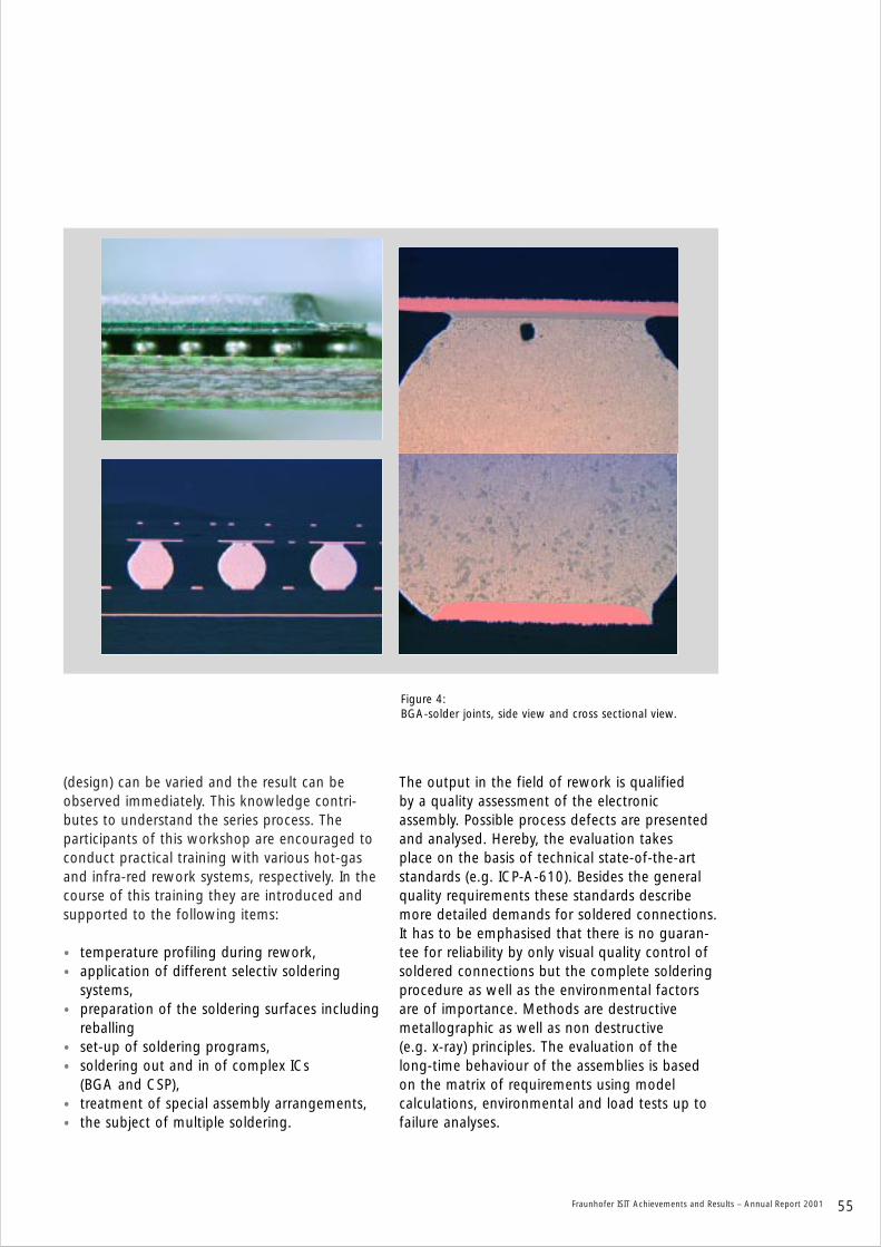
Fraunhofer ISIT Achievements and Results – Annual Report 2001 55
(design) can be varied and the result can beobserved immediately. This knowledge contri-butes to understand the series process. The participants of this workshop are encouraged toconduct practical training with various hot-gasand infra-red rework systems, respectively. In thecourse of this training they are introduced andsupported to the following items:
• temperature profiling during rework,• application of different selectiv soldering
systems,• preparation of the soldering surfaces including
reballing• set-up of soldering programs,• soldering out and in of complex ICs
(BGA and CSP), • treatment of special assembly arrangements,• the subject of multiple soldering.
The output in the field of rework is qualified by a quality assessment of the electronic assembly. Possible process defects are presentedand analysed. Hereby, the evaluation takes place on the basis of technical state-of-the-artstandards (e.g. ICP-A-610). Besides the generalquality requirements these standards describemore detailed demands for soldered connections.It has to be emphasised that there is no guaran-tee for reliability by only visual quality control ofsoldered connections but the complete solderingprocedure as well as the environmental factorsare of importance. Methods are destructivemetallographic as well as non destructive (e.g. x-ray) principles. The evaluation of the long-time behaviour of the assemblies is basedon the matrix of requirements using model calculations, environmental and load tests up tofailure analyses.
Figure 4: BGA-solder joints, side view and cross sectional view.


Important Names, Data, EventsAnnual Report 2001
58 Fraunhofer ISIT Achievements and Results – Annual Report 2001
Lecturing Assignments at Universities
H. Bernt:Halbleitertechnologie I und II, Technische Fakultät der Christian-Albrechts-Universität, Kiel
A. Heuberger:Lehrstuhl für Halbleitertechnologie,Christian-Albrechts-Universität, Kiel
P. Lange:Lehrbeauftragter Elektrotechnik, Fachhochschule Westküste, Heide
Memberships inCoordination Boards and Committees
T. Ahrens:Coordinator of AOI-Anwenderkreis(Automated Optical Inspection)
T. Ahrens:Member of DVS FachausschußLöten
T. Ahrens:Member of DVS FachausschußMikroverbindungstechnik
T. Ahrens:Member of Hamburger Lötzirkel
W. H. Brünger:Member of Steering Committee:Electron, Ion and Photon Beamsand Nanofabrication, EIPBN, USA
W. H. Brünger:Member of VDI Fachausschuß:Maskentechnik, VDI, Düsseldorf
W. H. Brünger:Section Head: Micro and NanoEngineering, MNE 01, Grenoble
T. Harder:Member of European Network˝Adhesives in Electronics˝
T. Harder:Member of European Network˝COMPETE˝
A. Heuberger:Advisory Editor of InternationalJournal of SemiconductorManufacturing Technology;Microelectronic Engineering
A. Heuberger:Member of NEXUS Board
A. Heuberger:Member of NEXUS ExcecutiveBoard
A. Heuberger:Member of NEXUS AcademicWorking Group
A. Heuberger:2. Chairman of an InternationalConference on Micro Electro,Opto, Mechanic Systems andComponents
R. Hintsche:National Delegate of COSTNanoscience & TechnologyAdvisory Group (NanoSTAG)
K. Pape:Member of VDI FachausschußAssembly Test, VDI, Frankfurt
K. Pape:Member of BVS, Bonn
K. Pape:Member of FED
H. C. Petzold:Member of NEXUS Executive Board
H. C. Petzold:Co-editor of mst news
M. Reiter:Member of Gf Korr “ArbeitskreisKorrosionsschutz in der Elektronik”
M. Reiter:Member of “ArbeitskreisLotpasten”
M. Reiter:Member of “Arbeitskreis BleifreieVerbindungstechnik in derElektronik”
M. Reiter:Member of “Industrie-ArbeitskreisKnow-How-Transfer mikrotechni-scher Produktion”
G. Zwicker:Head of Fachgruppe Planarisierung /Fachausschuss Verfahren / Fach-bereich Halbleitertechnologie und–fertigung der GMM des VDE/VDI
Cooperation withInstitutes and Universities
Institut für fluidtechnische Antriebeund Steuerungen, RWTH, Aachen
Institut für Werkstoffe derElektrotechnik, RWTH, Aachen
Aalborg University, Aalborg,Denmark
Hahn-Meitner-Institut, Berlin
Technische Universität Berlin
TU Braunschweig, FachbereichElektrotechnik, Institut fürElektrophysik
Technical University of Budapest,Department of ElectronicTechnology, Budapest, Ungarn
Cambridge University, UK
Rutherford Appleton Laboratories,Didicot, UK
TU Dresden, Institut für Halbleiter-und Mikrosystemtechnik
Karl-Franzens University, Graz,Austria
Ernst-Moritz-Arndt-Universität(EMAU), Greifswald
CEA Leti, Grenoble, France
Max-Planck-Institut fürMikrostrukturphysik, Halle
UniversitätskrankenhausEppendorf, Hamburg
Universität Hamburg, Abteilung fürBiochemie und Molekularbiologie
Fachhochschule Westküste, Heide
University of Technology, Helsinki,Finland
Institut für Fügetechnik undWerkstoffprüfung (IFW), Jena
Christian-Albrechts-Universität,Technische Fakultät und Institut fürMeereskunde, Kiel
FH Kiel
IEMN-ISEN, Lille, France
City University, London, UK
Important Names, Data, Events
Fraunhofer ISIT Achievements and Results – Annual Report 2001 59
University of Southern California,Los Angeles, USA
Université catholique de Louvain,Louvain-la-Neuve, Belgium
Fachhochschule Lübeck
CNRS-Université Claude Benard,Lyon, France
TU München
Universität der Bundeswehr,München
SINTEF, Oslo, Norway
Universität Oulu, Finland
Rutherford Appleton LaboratoryOxford, UK
University of Perugia, Perugia, Italy
Royal Institute of Technology(KTH), Stockholm, Sweden
VDI/VDE-TechnologenzentrumInformationstechnik, Teltow
Fachhochschule Wedel
Technische Universität Wien,Austria
Trade Fairs andExhibitions
Flip Chip & Chip Scale Europe 2001. International Convention &Exhibition on Innovative ElectronicPackaging and AssemblyTechnologies, March 21 – March 22, 2001,Böblingen
Hannover Messe 2001, AMA Sensorik Centrum.April 23 – April 28, 2001,Hannover
Hannover Messe 2001,Innovation Market for Research and Development.April 23 – April 28, 2001,Hannover
SMT/ES&S/Hybrid 2001. System Integration in MicroElectronics, Exhibition andConference, April 24 – April 26, 2001,Nürnberg
Sensor 2001. 10th International Trade Fair andInternational Congress: "Sensoren,Messaufnehmer und Systeme”.May 8 – May 10, 2001, Nürnberg
Laser 2001. 15th International Trade Fair andInternational Congress, June 18 – June 22, 2001,München
Productronica 2001.14th International Trade Fair forElectronic Production, November 6 – November 9, 2001,München
Miscellaneous Events
“Aspekte moderner Siliziumtech-nologie” Public lectures. Monthlypresentations, ISIT Itzehoe
“Inspektion in der Baugruppen-fertigung” Seminar. February 7 – February 8, 2001, ISIT Itzehoe
“Mikrotechnologie: Arbeitsplätzeder Zukunft”. Information eventand press conference. Speakers:Michael Rocca, Staatssekretär imMinisterium für Wirtschaft,Technologie und Verkehr desLandes Schleswig-Holstein, Prof.Anton Heuberger, ISIT, Hans-Joachim Ramlow, ÜAZ, February 14, 2001, ISIT Itzehoe
“Manuelles Löten von SMT-Bauelementen” Seminar. February 21 – February 23, 2001, ISIT Itzehoe
“Der Lötprozess in derElektronikfertigung” Seminar.March 5 – March 7, 2001, ISIT Itzehoe
“SMT-Rework-Praktikum” Seminar.April 4 – April 5, 2001, ISIT Itzehoe
“Direktmontage ungehäusterBauelemente” Seminar. May 16 – May 17, 2001, ISIT Itzehoe
ISIT-, Vishay-Presentation at “Tagder beruflichen Bildung” organizedby Berufliche Schule des KreisesSteinburg. July 17, 2001, Itzehoe
“Mobiles SMT-Rework-Praktikum”Seminar. September 5 – September 6, 2001, DVS,Düsseldorf
ISIT, Vishay-Presentation at “Tag der Ausbildung” organized byÜAZ Itzehoe. September 15, 2001,Itzehoe
“Direktmontage ungehäusterBauelemente” Seminar. September 19 – September 20, 2001,ISIT Itzehoe
“Der Lötprozess in derElektronikfertigung” Seminar.October 15 – October 17, 2001,ISIT Itzehoe
“Manuelles Löten von SMT-Bau-elementen” Seminar. November 14 – November 16, 2001, ISIT Itzehoe
“SMT-Rework-Praktikum” Seminar.November 14 – November 16,2001, ISIT Itzehoe
“Erfolgreiche Integration des CEMin das Fraunhofer ISIT” Press conference. Speakers: Prof. Detlefvon Hofe, Deutscher Verband fürSchweißen und verwandteVerfahren, Dr. Joachim Scholz,Fachverband für Sensorik e.V.,Karin Pape, ISIT, Prof. AntonHeuberger, ISIT, December 20,2001, ISIT Itzehoe
60 Fraunhofer ISIT Achievements and Results – Annual Report 2001
Journal Papers and Contributions toConference
T. Ahrens:Zerstörungsfreie Prüfung in derQualitätsbewertung elektronischerBaugruppen.VTE – Aufbau- und Verbindungs-technik in der Elektronik 4, p.194-203, August, 2001
T. Ahrens:Elektronische Baugruppen zerstö-rungsfrei prüfen.VTE – Aufbau- und Verbindungs-technik in der Elektronik 6, p.305-313, December, 2001
M. Christophersen, P. Merz, J. Quenzer, J. Carstensen, H. Föll:Deep Electrochemical TrenchEtching with Organic HydrofluoricElectrolytes.Sensors and Actuators A, 88 (3) ,p. 241-246, 2001
T. Harder, W. Reinert:Low-Profile Flip Chip Assemblyusing Ultra-Thin ICs. Proceedingsof 13th European Microelectronicsand Packaging Conf. (IMAPS), p.310, Strasbourg May, June, 2001
W.I. Milne, K. B. K. Teo, M. Chhowalla, G. A. Amaratunga,J. Yuan, J. Robertson, P. Legagneux, G. Pirio, D. Pribat,K. Bouzehouane, W. H. BrüngerC. Trautmann:Carbon Films for Use as the ElectronSource in a Parallel e-Beam Litho-graphy System. New Diamond andFrontier Carbon Technology Vol 11,No.4, p. 235, 2001
H. Pristauz, W. Reinert:Handling Concepts for Ultra-ThinWafers. Proceedings of 13thEuropean Microelectronics andPackaging Conf. (IMAPS),Strasbourg p. 336, May, June,2001
O. Schwarzelbach, G. Fakas, W. Nienkirchen:New Approach for FrequencyMatching of Tuning ForkGyrocopes by Using a NonlinearDriving Concept. Proceedings ofTransducers 01 11 th InternationalConference on Solid-State Sensorsand Actuators, p. 464-467, June 10 – June 14, 2001
V. Sukhorukov, M. Kürschner, S. Dilky, T. Lisec, B. Wagner, W. A. Schenk, R. Benz, U. Zimmermannn:Phloretic-Induced Changes ofLipophilic Ion Transport across thePlasma Membrane of MammalianCells. Biophysical Journal, Vol. 81, p. 1006-1013, 2001
Talks and PosterPresentations
T. Ahrens:Rework komplexer SMT-Baugruppen.Seminar: Manuelles Löten vonSMT- Bauelementen, ISIT, Itzehoe,February 21, 2001
T. Ahrens:Lötqualität. Seminar: Der Lötprozessin der Fertigung elektronischerBaugruppen, ISIT, Itzehoe, March 5,2001
T. Ahrens:Rework-Strategien. Seminar: DerLötprozess in der Fertigung elektro-nischer Baugruppen, ISIT, Itzehoe,March 6, 2001
T. Ahrens:Einbau der Zuverlässigkeit.Seminar: Der Lötprozess in derFertigung elektronischerBaugruppen, ISIT, Itzehoe, March 7, 2001
T. Ahrens:Rework and Repair von elektroni-schen Baugruppen.4. Europäische Elektroniktechnologie-Kolleg, Colonia St. Jordi, Mallorca,Spanien, March 16, 2001
T. Ahrens: Rework-Strategien.Der Lötprozess in der Fertigungelektronischer Baugruppen, ISIT,Itzehoe, October 15, 2001
T. Ahrens:Baugruppen- und Fehlerbewertung.Seminar: Der Lötprozess in derFertigung elektronischer Bau-gruppen, ISIT, Itzehoe, October 16,2001
T. Ahrens:Lötqualität.Seminar: Der Lötprozess in der Fer-tigung elektronischer Baugruppen,ISIT, Itzehoe, October 16, 2001
Scientific Publications
62 Fraunhofer ISIT Achievements and Results – Annual Report 2001
Diploma Theses
L. Blohm:Realisierung der drahtlosenAnbindung eines µC-gesteuertenMessgerätes an eine PC-Plattformin Verbindung mit der Optimierungder Datenerfassungs- undSteuersoftware.Fachhochschule Westküste, Heide,2001
U. Bott:Untersuchung und Weiterentwick-lung eines Herstellungsprozessesvon Mikrolinsen auf Glassubstraten.Fachhochschule Lübeck, 2001
C. Werlich:Entwicklung eines autarkenGatetreiberbausteins für Zuverlässigkeitsuntersuchungen.Fachhochschule Westküste, Heide,2001
Scientific Publications
Fraunhofer ISIT Achievements and Results – Annual Report 2001 63
Overview of Projects
• Hochtemperatur-Elektronik-Studie
• Entwicklung von Super-Junction-Strukturen für Hochvolt-PowerMOS-Anwendungen
• Halbleiterbauelemente hoherLeistung
• Entwicklung einer Fertigungs-technologie für NPT-Trench-IGBTsim Spannungsbereich bis 1.2 KV
• Entwicklung eines Prozess-moduls zur Herstellung lokalerWärmesenken auf vollständigprozessierten BCDMOS Wafern
• Prozessierung von Wafern mittelsSilizium-Trockenätzen zur Erzeugung spezieller Si-Strukturen
• Fabrication of CapacitorStructures
• Development of a Metal ResistorProcess Module and its Integrationinto an Existing ID-Process
• Evaluierung eines IR-Ofens zurthermischen Behandlung dickerLacke, IR BAKER
• Fabrication of Inductor Structures
• Prozessentwicklung zurHerstellung von Nonostrukturenin Siliziumnitrid
• Herstellung von SiGe Bragg-Gittern
• Optische Reflexionsgitter aufTantalpentoxid
• Einsatz der Ionen-Projektions-Lithographie im Fertigungs-prozess für die kontaktloseStrukturierung planarer, magnetischer Speichermedien
• Kalte Ionenquelle für die Ionen-Projektions-Lithographie
• Ausgasverhalten von e-beam-Lacken
• Arrays of Microguns for Parallele-Beam Nanolithography,NANOLITH
• Entwicklung von Post-CMP-Reinigungsprozessen für dieFertigung von zukünftigen integrierten Schaltkreisen in derSi-Technologie
• Erprobung eines Post-CMP-Reinigungssystems auf der Basisdes Jet-Steam-Cleaning für300mm Wafer
• Aufstellung und Erprobungeiner Waferreinigungsanlage auf der Basis von Ozon mit kryomagnetischer Silizium-scheibenlagerung
• Evaluierung von Slurries zumchemisch-mechanischen Polierenvon SiO2
• Planarisierung von Glaswafern
• Prozessentwicklung für dieHerstellung von terrasiertenSilizium-Strukturen
• Maskenentwurf für “IntegratedDiscretes”
• Developement of an MicroGyroscope (Mechanics andElectronics), STARS
• Entwicklung eines ASICs fürAutomotive-Anwendungen(LIBRA)
• Entwurf einer 1/0- Schaltung fürHandy-Anwendungen
• Untersuchung an mikromecha-nischen Drehraten-Sensoren
• Entwicklung eines mikromecha-nischen Luftmassensensors
• Entwicklung eines in Silizium-technologie hergestellten pneumatischen 3/2-Wege-Mikroventils
• European Access to Manu-facturing Service for MEMS onSOI Micromachining Technologies
• Herstellung und Replikation vongroßflächigen 3D-Nano- undMikrostrukturen, NanoFab
• Entwicklung von kapazitiven HF-Schaltern
• Herstellung eines statischenSpiegel-Arrays mit Grauton-Lithographie
• Entwicklung und Herstellungvon Flowsensoren
• Musterfertigung von Blenden-karten mit Soft-Blenden
• Fertigung eines Spiegelarraysmit elektrischem Anschluß undBeurteilung der Mikrospiegel-technologie
• Micro Well Plates with Trans-parent Stimulation Electrodes
• Entwicklung eines 4x4 Arraysvon Zweiachsen-Mikrospiegeln
• Fabrication, Assembly andTesting of a Miniature Two-AxisLaser Scanner and a HighVoltage Amplifier
• Micromachined ElectromechanicalDevices for Integrated WirelessCommunication Transceivers,MELODICT
• Entwicklung eins modularenMikroanalysesystems, EASY-LAB
• Micro-Scanning Endoscope with Diagnostic and AnhancedResolution Attributes
• Entwicklung eines Spektrometersmit Stufenplatten
• Herstellung von Nanolichtquellenzur hochauflösenden Inspektionvon biologischen Proben
• Kostengünstige Herstellung vonMikrosystemen: Verbundtechnikvon Kunststoff und Silizium(MP-CC)
• Entwicklung eines hochdruck-festen Drucksensors
• Herstellung mikrooptischerLinsenarrays aus Glas
• Electric DNA Chips for BioprocessControl
• Integriertes mikrobiologischesSensorsystem zur Abwasser-analyse
• Silizium-Chipsystem für die biochemische Analysentechnik:Technologische Plattform undSystemintegration Teilvorhaben:Messverfahren und bio-chemische Assays
• Silizium-Chipsystem für die biochemische Analysentechnik:Technologische Plattform undSystemintegration, Teilvorhaben:Testchips und Testverfahren
• Entwicklung von Ultramikro-elektrodenarrays und Integrationin ein automatisiertes fluidischesAnalysesystem
• Advanced Insulin Infusion Usinga Control Loop
• Festkörper-Lithiumakkumulatoren
• Manufacturing Cluster, EUROPRACTICE III MC 1
• Network of Excellence inMultifunctional Microsystems,NEXUS 2000
• Customer Support and DesignCentre for Physical MeasurementSystems, EUROPRACTICE IIICCMeSys
• Microactuator CompetenceCentre, EUROPRACTICE IIICCMicro
• Alternatives Löten von Mikrobau-steinen
• Laserlöten von Silizium-Pyrexmittels Glaslot zur Kapselungvon Mikrosensoren
• Mikrosystemtechnik 2000+, µ-Encoder mit zentrischer optischer Abtastung
• Bonden mit Cu-Draht in derLeistungselektronik
• Flip-Chip-Technologie mitgedünnten Siliziumchips fürintelligente Etiketten (Smart-Label)
• Chipkartenbestückung mitGrautonblenden
• Ultra-Thin Packaging Solutionsusing Thin Silicon
• Thematic Network “Adhesives inElectronics”
• Flip Chip Die Bonder for Ultra-Thin Silicon
• Herstellung porenarmer Weich-lötverbindungen
• Reflow und Wellenlöten mitbleifreien Loten
• Zuverlässigkeit mikrotechnischerLötverbindungen
• Die elektronische Baugruppe derZukunft
• Modulintegration und Gehäuse-technik für großflächige Mikro-systeme
• Stressoptimierte Montage undGehäusetechnik für mikrome-chanisch hergestellte Silizium-Drehratensensoren
General View on Projects
Imprint
Editor Claus Wacker
Layout / SettingAnne Brodmeier, Hamburg
LithographyTypoDesign GmbH, Hamburg
PrintingBeisner Druck GmbH, Hamburg
Photographs:Title, pp. 10, 14, 15, 17 top, 19, 20 bottom, 36, 40 top, 46, 53 photo company Itzehoe
p. 51 Technolas
other pictures ISIT
Contact
Please contact us for further information. We would be glad to answer your questions.
Fraunhofer-Institutfür Siliziumtechnologie ItzehoeFraunhoferstraße 125524 ItzehoeTelephone +49(0) 4821 / 17-4211 (Secretary)Fax +49(o) 4821 / 17-4251e-mail [email protected]://www.isit.fhg.de
Press and Public RelationsClaus WackerTelephone +49 (0) 48 21 / 17-42 14email [email protected]