Embed Size (px)
Citation preview
Abstract This paper proposes a novel flexible display technologies using ultra-thin glass substrate. Flexible thin glass substrate as a panel material for TFTs are proposed for the energy saving. There are many attractive applications for such TFTs on thin glass like highly functional systems, and rather simple paper displays and printable displays. They are suitable as high performance mobile terminals. The Si based TFTs crystallized using semiconductor blue laser have an advantage as a highly functional panel by improving the performance with reducing the production cost. The device structure of organic TFTs on thin flexible glass is more suitable for reducing drastically an energy cost in which the semiconductor layer may be coated by a spin coating method.
Low energy-cost TFT technologies using ultra-thin flexible glass substrateNoriyoshi Yamauchi1, Taketsugu Itoh2 and Takashi Noguchi3
1Information, Production and Systems, Waseda University, Kitakyushu, Japan2Corning Holding Japan G.K., Tokyo, Japan
3Faculty of Engineering, University of the Ryukyu, Okinawa, Japan
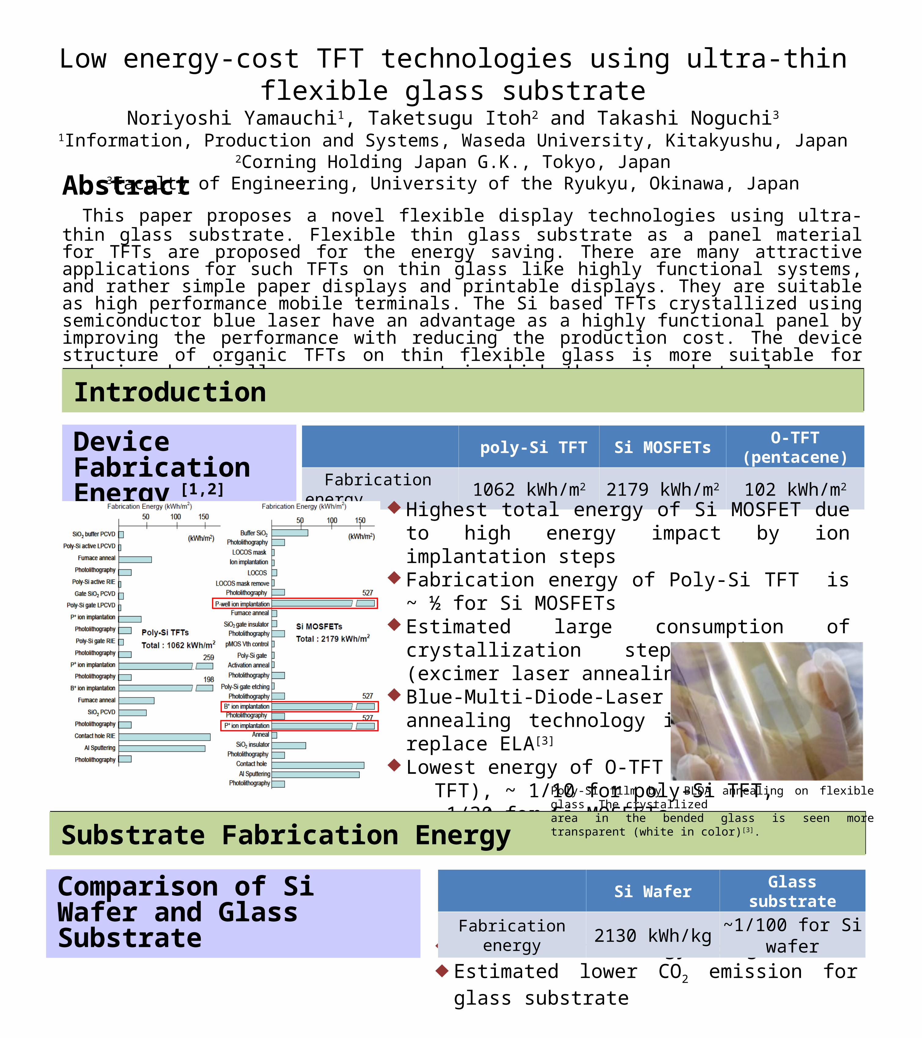
Device Fabrication Energy [1,2]
poly-Si TFT Si MOSFETs O-TFT (pentacene)
Fabrication energy 1062 kWh/m2 2179 kWh/m2 102 kWh/m2
Highest total energy of Si MOSFET due to high energy impact by ion implantation steps
Fabrication energy of Poly-Si TFT is ~ ½ for Si MOSFETs Estimated large consumption of crystallization step
using ELA (excimer laser annealing) for LTPS Blue-Multi-Diode-Laser (BLDA) annealing technology is
available to replace ELA[3] Lowest energy of O-TFT (organic TFT), ~ 1/10 for poly-Si TFT, 1/30 for Si MOSFETs
IntroductionIntroduction
Substrate Fabrication Energy Substrate Fabrication Energy
Low substrate energy for glass Estimated lower CO2 emission for glass substrate
Si Wafer Glass substrate
Fabrication energy 2130 kWh/kg ~1/100 for Si waferComparison of Si Wafer and Glass Substrate
Poly-Si film by BLDA annealing on flexible glass. The crystallized area in the bended glass is seen more transparent (white in color)[3].
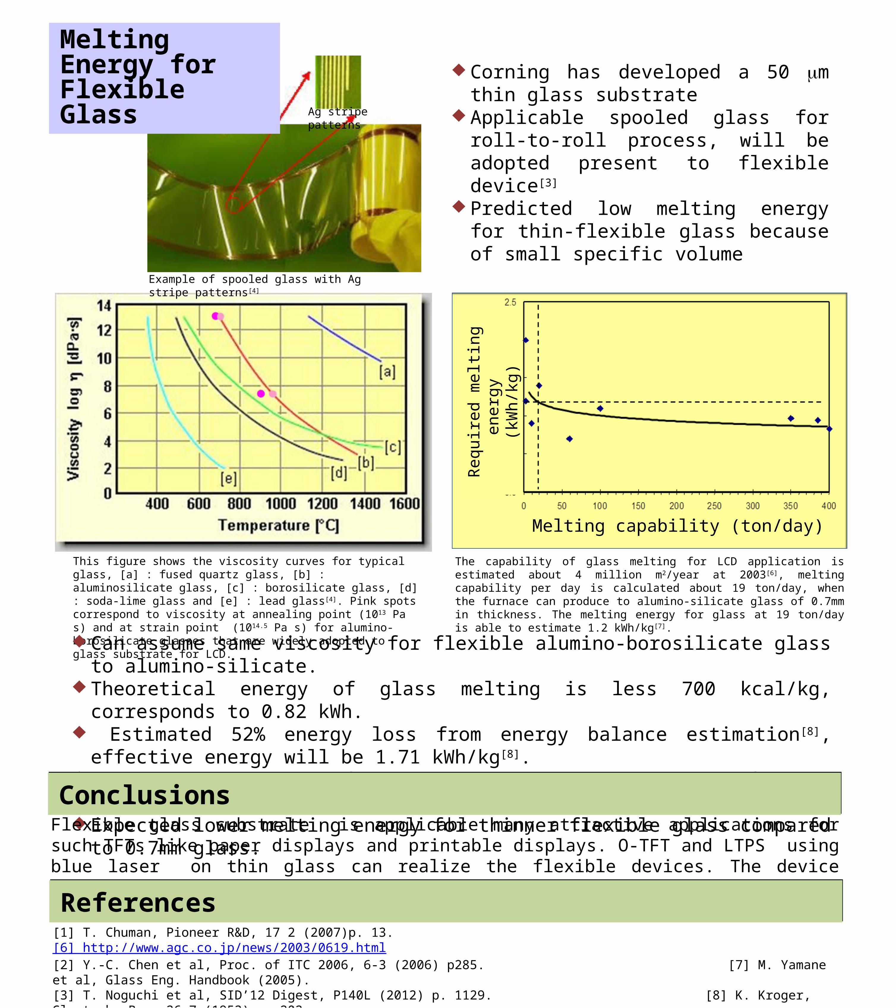
This figure shows the viscosity curves for typical glass, [a] : fused quartz glass, [b] : aluminosilicate glass, [c] : borosilicate glass, [d] : soda-lime glass and [e] : lead glass[4]. Pink spots correspond to viscosity at annealing point (1013 Pa s) and at strain point (1014.5 Pa s) for alumino-borosilicate glasses that are widely adopted to glass substrate for LCD.
Melting capability (ton/day)
Requ
ired
mel
ting
ener
gy
(kW
h/kg
)
Corning has developed a 50 m thin glass substrate
Applicable spooled glass for roll-to-roll process, will be adopted present to flexible device[3]
Predicted low melting energy for thin-flexible glass because of small specific volume
Melting Energy forFlexible Glass
Example of spooled glass with Ag stripe patterns[4]
Can assume same viscosity for flexible alumino-borosilicate glass to alumino-silicate. Theoretical energy of glass melting is less 700 kcal/kg, corresponds to 0.82 kWh. Estimated 52% energy loss from energy balance estimation[8], effective energy will be 1.71
kWh/kg[8]. Estimated 1.2 kWh/kg from practical melting capability for LCD glass industry. Expected lower melting energy for thinner flexible glass compared to 0.7mm glass.
ConclusionsConclusionsFlexible glass substrate is applicable many attractive applications for such TFTs like paper displays and printable displays. O-TFT and LTPS using blue laser on thin glass can realize the flexible devices. The device structure on thin glass is more suitable in term of energy saving.
Ag stripe patterns
The capability of glass melting for LCD application is estimated about 4 million m2/year at 2003[6], melting capability per day is calculated about 19 ton/day, when the furnace can produce to alumino-silicate glass of 0.7mm in thickness. The melting energy for glass at 19 ton/day is able to estimate 1.2 kWh/kg[7].
ReferencesReferences[1] T. Chuman, Pioneer R&D, 17 2 (2007)p. 13. [6] http://www.agc.co.jp/news/2003/0619.html[2] Y.-C. Chen et al, Proc. of ITC 2006, 6-3 (2006) p285. [7] M. Yamane et al, Glass Eng. Handbook (2005).[3] T. Noguchi et al, SID’12 Digest, P140L (2012) p. 1129. [8] K. Kroger, Glastech. Ber, 26 7 (1953) p. 202.[4] S. Garner et al, SID’12 Digest, 26.1(2012) p.342. [5] M. Lindig, ,Glass (2004) p. 294.