Embed Size (px)
Citation preview

General DescriptionThe MAX16930/MAX16931 offer two high-voltage, synchronous step-down controllers and a step-up preboost controller. They operate with an input voltage supply from 2V to 42V with preboost active and can “operate in drop-out condition by running at 95% duty cycle. The devices are intended for applications with mid- to high-power requirements that operate at a wide input voltage range such as during automotive cold-crank or engine stop-start conditions.
The MAX16930/MAX16931 step-down controllers operate 180° out-of-phase at frequencies up to 2.2MHz to allow small external components, reduced output ripple, and to guarantee no AM band interference. The switching frequency is resistor adjustable. The FSYNC input programmability enables three frequency modes for optimized performance: forced fixed-frequency operation, skip mode with ultra-low quiescent current (20µA), and synchronization to an external clock. The devices also provide a spread-spectrum option to minimize EMI interference.
The MAX16930/MAX16931 are offered with an asynchronous step-up controller. This preboost cir-cuitry turns on during low input voltage conditions. It is designed to provide power to step-down controller chan-nels with input voltages as low as 2V.
The devices also feature a power-OK monitor and overvoltage and undervoltage lockout. Protection features include cycle-by-cycle current limit and thermal shutdown.
The devices are available in 40-pin TQFN-EP and side-wettable QFND-EP packages and are specified for operation over the -40°C to +125°C automotive temperature range.
Benefits and Features Meets Stringent OEM Module Power Consumption
and Performance Specifications• 20µA Quiescent Current in Skip Mode• ±1% Output-Voltage Accuracy: 5.0V/3.3V Fixed or
Adjustable Between 1V and 10V Enables Crank-Ready Designs
• Integrated Preboost for Operation Down to 2V in Bootstrap Mode
• Wide Input Supply Range from 3.5V to 36V (without Preboost)
EMI Reduction Features Reduce Interference with Sensitive Radio Bands without Sacrificing Wide Input Voltage Range• 50ns (typ) Minimum On-Time Guarantees Skip-
Free Operation for 3.3V Output from Car Battery at 2.2MHz
• Frequency-Synchronization Input• Resistor-Programmable Frequency Between
200kHz and 2.2MHz Integration and Thermally Enhanced Packages Save
Board Space and Cost• Dual, 2MHz Step-Down Controllers • 180° Out-of-Phase Operation• Current-Mode Controllers with Forced-Continuous
and Skip Modes • Thermally Enhanced 40-Pin TQFN-EP and
Side-Wettable QFND-EP Packages Protection Features Improve System Reliability
• Supply Overvoltage and Undervoltage Lockout• Overtemperature and Short-Circuit Protection
ApplicationsPOL Applications for Automotive Power
Distributed DC Power Systems
Navigation and Radio Head UnitsSelector Guide and Ordering Information appear at end of data sheet.
19-6631; Rev 13; 7/16
MAX16930/MAX16931 2MHz, 36V, Dual Buck with Preboost and 20µA Quiescent Current

IN, INS, CS3P, CS3N, FB3, EN1, EN2, EN3, TERM to PGND_ .......................................-0.3V to +42V
CS1, CS2, OUT1, OUT2 to AGND ........................-0.3V to +11VCS1 to OUT1 ........................................................-0.2V to +0.2VCS2 to OUT2 ........................................................-0.2V to +0.2VCS3P to CS3N ......................................................-0.2V to +0.2V BIAS, FSYNC, FOSC to AGND .............................-0.3V to +6.0VCOMP1, COMP2, BSTON to AGND .....................-0.3V to +6.0VFB1, FB2, FSELBST, EXTVCC to AGND ..............-0.3V to +6.0VDL_ to PGND_ (Note 1) ........................................-0.3V to +6.0VBST_ to LX_ (Note 1) ...........................................-0.3V to + 6.0VDH_ to LX_ (Note 1) ............................................-0.3V to + 6.0V
LX_ to PGND_ (Note 1) .........................................-0.3V to +42VPGND_ to AGND ..................................................-0.3V to +0.3VPGOOD1, PGOOD2 to AGND.......... ...................-0.3V to +6.0VContinuous Power Dissipation (TA = +70NC)
TQFN (derate 37mW/NC above +70NC).....................2963mW QFND (derate 29.4mW/NC above +70NC)............ .....2350mWOperating Temperature Range. ....................... -40NC to +125NCJunction Temperature Range ..........................................+150NCStorage Temperature Range ............................ -65NC to +150NCLead Temperature (soldering, 10s) ................................+300NCSoldering Temperature (reflow)...................................... +260NC
TQFN Junction-to-Ambient Thermal Resistance (qJA) ..........27°C/W Junction-to-Case Thermal Resistance (qJC) .................1°C/W
QFND Junction-to-Ambient Thermal Resistance (qJA) ..........34°C/W Junction-to-Case Thermal Resistance (qJC) ..............3.9°C/W
Absolute Maximum Ratings
Note 1: Self-protected against transient voltages exceeding these limits for ≤ 50ns under normal operation and loads up to the maximum rated output current.
Note 2: Package thermal resistances were obtained using the method described in JEDEC specification JESD51-7, using a four-layer board. For detailed information on package thermal considerations, refer to www.maximintegrated.com/thermal-tutorial.
Stresses beyond those listed under “Absolute Maximum Ratings” may cause permanent damage to the device. These are stress ratings only, and functional opera-tion of the device at these or any other conditions beyond those indicated in the operational sections of the specifications is not implied. Exposure to absolute maximum rating conditions for extended periods may affect device reliability.
Package Thermal Characteristics (Note 2)
Electrical Characteristics(VIN = 14V, VBIAS = 5V, CBIAS = 6.8µF, TA = TJ = -40NC to +125NC, unless otherwise noted.) (Note 3)
MAX16930/MAX16931 2MHz, 36V, Dual Buck with Preboost and 20µA Quiescent Current
www.maximintegrated.com Maxim Integrated 2
PARAMETER SYMBOL CONDITIONS MIN TYP MAX UNIT
SYNCHRONOUS STEP-DOWN DC-DC CONVERTERS
Supply Voltage Range VIN
Normal operation 3.5 36
Vt < 1s 42
With preboost after initial startup condition is satisfied
2.0 36
Supply Current IIN
VEN1 = VEN2 = VEN3 = 0V 8 20
FA
VEN1 = 5V, VOUT1 = 5V, VEN2 = VEN3 = 0V, VEXTVCC = 5V, no switching
30 40
VEN2 = 5V, VOUT2 = 3.3V, VEN1 = VEN3 = 0V, VEXTVCC = 3.3V, no switching
20 30
VEN1 = VEN2 = 5V, VOUT1 = 5V, VOUT2 = 3.3V, VEN3 = 0V, VEXTVCC = 3.3V, no switching
25 40
Buck 1 Fixed Output Voltage VOUT1VFB1 = VBIAS, PWM mode 4.95 5 5.05
VVFB1 = VBIAS, skip mode 4.95 5 5.075
Buck 2 Fixed Output Voltage VOUT2VFB2 = VBIAS, PWM mode 3.234 3.3 3.366
VVFB2 = VBIAS, skip mode 3.234 3.3 3.4
Output Voltage Adjustable Range
Buck 1, buck 2 1 10 V

Electrical Characteristics (continued)(VIN = 14V, VBIAS = 5V, CBIAS = 6.8µF, TA = TJ = -40NC to +125NC, unless otherwise noted.) (Note 3)
MAX16930/MAX16931 2MHz, 36V, Dual Buck with Preboost and 20µA Quiescent Current
www.maximintegrated.com Maxim Integrated 3
PARAMETER SYMBOL CONDITIONS MIN TYP MAX UNIT
Regulated Feedback Voltage VFB1,2 0.99 1.0 1.01 V
Output Overvoltage ThresholdFB rising +10 +15 +20
%FB falling (Note 4) +5 +10 +15
Feedback Leakage Current IFB1,2 TA = +25NC 0.01 1 FA
Feedback Line Regulation Error VIN = 3.5V to 36V, VFB = 1V 0.00 %/V
Transconductance(from FB_ to COMP_)
gm VFB = 1V, VBIAS = 5V (Note 5) 1200 2400 FS
Dead Time
MAX16930, DL_ low to DH_ high 35
nsMAX16930, DH_ low to DL_ high 60
MAX16931, DL_ low to DH_ high 60
MAX16931, DH_ low to DL_ high 100
Maximum Duty-Cycle Buck 1, buck 2 95 %
Minimum On-Time tON(MIN) Buck 1, buck 2 50 ns
PWM Switching Frequency Range
Programmable, high frequency, MAX16930
1 2.2MHz
Programmable, low frequency,MAX16931
0.2 1
Buck 2 Switching Frequency MAX16930ATLT/V+, MAX16930BATLU/V+ only
1/2fSW MHz
Switching Frequency Accuracy fSW
MAX16930, RFOSC = 13.7kI, VBIAS = 5V
1.98 2.2 2.42 MHz
MAX16931, RFOSC = 80.6kI, VBIAS = 5V
360 400 440 kHz
Spread-Spectrum Range Spread spectrum enabled ±6 %
FSYNC INPUT
FSYNC Frequency RangeMinimum sync pulse of 100ns, MAX16930 1.2 2.4 MHz
Minimum sync pulse of 100ns, MAX16931 240 1200 kHz
FSYNC Switching ThresholdsHigh threshold 1.5
VLow threshold 0.6
CS Current-Limit Voltage Threshold
VLIMIT1,2 VCS - VOUT, VBIAS = 5V, VOUT R 2.5V 64 80 96 mV
Skip Mode Threshold Current sense = 80mV 15 mV
Soft-Start Ramp TimeBuck 1 and buck 2, fixed soft-start time regardless of frequency
2 6 10 ms
Phase Shift Between Buck1 and Buck 2
180 °
LX1, LX2 Leakage Current VIN = 6V, VLX_ = VIN, TA = +25NC 0.01 1 FA
DH1, DH2 Pullup Resistance VBIAS = 5V, IDH_ = -100mA 10 20 I
DH1, DH2 Pulldown Resistance VBIAS = 5V, IDH_ = +100mA 2 4 I

Electrical Characteristics (continued)(VIN = 14V, VBIAS = 5V, CBIAS = 6.8µF, TA = TJ = -40NC to +125NC, unless otherwise noted.) (Note 3)
MAX16930/MAX16931 2MHz, 36V, Dual Buck with Preboost and 20µA Quiescent Current
www.maximintegrated.com Maxim Integrated 4
PARAMETER SYMBOL CONDITIONS MIN TYP MAX UNIT
DL1, DL2 Pullup Resistance VBIAS = 5V, IDL_ = -100mA 4 8 I
DL1, DL2 Pulldown Resistance VBIAS = 5V, IDL_ = +100mA 1.5 3 I
PGOOD1, PGOOD2 ThresholdPGOOD_H % of VOUT_, rising 85 90 95
%PGOOD_F % of VOUT_, falling 80 85 90
PGOOD1, PGOOD2 Leakage Current
VPGOOD1,2 = 5V, TA = +25NC 0.01 1 FA
PGOOD1, PGOOD2 Startup Delay Time
Buck 1 and buck 2 after soft-start is complete
64 Cycles
PGOOD1, PGOOD2 Debounce Time
Fault detection 8 20 40 Fs
INTERNAL LDO: BIAS
Internal BIAS Voltage VIN > 6V 4.75 5 5.25 V
BIAS UVLO ThresholdVBIAS rising 3.1 3.4
VVBIAS falling 2.7 2.9
Hysteresis 0.2 V
External VCC Threshold VTH,EXTVCC EXTVCC rising, HYST = 110mV 3 3.2 V
THERMAL OVERLOAD
Thermal Shutdown Temperature (Note 5) 170 NC
Thermal Shutdown Hysteresis (Note 5) 20 NC
EN LOGIC INPUT
High Threshold 1.8 V
Low Threshold 0.8 V
Input Current EN1, EN2 logic inputs only, TA = +25NC 0.01 1 FA
PREBOOST
Minimum On Time TONBST 60 ns
Minimum Off Time TOFFBST 60 ns
Switching Frequency fBOOSTVFSELBST = 0V, RFOSC = 13.7kI 1.98 2.2 2.42
MHzVFSELBST = VBIAS, RFOSC = 13.7kI 0.4 0.44 0.48
Current Limit ILIMBST CS3P - CS3N 108 120 132 mV
INS Unlock Threshold VINS,UV
One-time latch during startup; preboost is disabled until the VINS rises above this threshold (MAX16930ATLV/V+, MAX16930BATLW/V+ (Note 6))
1 1.05 1.1 V

Note 3: Limits are 100% production tested at TA = +25°C. Limits over the operating temperature range and relevant supply volt-age are guaranteed by design and characterization. Typical values are at TA = +25°C.
Note 4: Overvoltage protection is detected at the FB1/FB2 pins. If the feedback voltage reaches overvoltage threshold of FB1/FB2 + 15% (typ), the corresponding controllers stop switching. The controllers resume switching once the output drops below FB1/FB2 + 10% (typ).
Note 5: Guaranteed by design; not production tested.Note 6: INS pin functionality is disabled for the MAX16930ATLV/V+, MAX16930BATLW/V+. EN3 directly controls the turn-on and
turn-off of the boost controller.
Electrical Characteristics (continued)(VIN = 14V, VBIAS = 5V, CBIAS = 6.8µF, TA = TJ = -40NC to +125NC, unless otherwise noted.) (Note 3)
MAX16930/MAX16931 2MHz, 36V, Dual Buck with Preboost and 20µA Quiescent Current
www.maximintegrated.com Maxim Integrated 5
PARAMETER SYMBOL CONDITIONS MIN TYP MAX UNIT
INS Off Threshold VINS,OFF
Battery rising and EN3 high, preboost turns off if VINS is above this threshold (MAX16930ATLV/V+, MAX16930BATLW/V+ (Note 6))
1.2 1.25 1.3
V
INS On Threshold VINS,ON,SW
Battery falling and EN3 high, preboost turns back on when VINS falls below this threshold (MAX16930ATLV/V+, MAX16930BATLW/V+ (Note 6))
1.1 1.15 1.2
INS ThresholdUndervoltage Lockout
VINS,UV
Battery rising and EN3 high (MAX16930ATLV/V+, MAX16930BATLW/V+ (Note 6))
0.325 0.35 0.375
VBattery falling and EN3 high, preboost turns off when VINS falls below this threshold (MAX16930ATLV/V+, MAX16930BATLW/V+ (Note 6))
0.275 0.3 0.325
BSTON Leakage Current VBSTON = 5V, TA = +25NC 0.01 1 FA
BSTON Debounce Time Fault detection 10 Fs
DL3 Pullup Resistance VBIAS = 5V, IDL3 = -100mA 4 8 I
DL3 Pulldown resistance VBIAS = 5V, IDL3 = +100mA 1 2 I
Feedback Voltage VFB3 No load on boost output 1.1875 1.25 1.3125 V
Boost Load Regulation Error0mV < VCS3P - VCS3N < 120mV, error proportional to input current
0.7 %/A
EN3 ThresholdHigh threshold 3.5
VLow threshold 2
EN3 Input Current VEN3 = 5.5V 7 14 FA
TERM Resistance ITERM = 10mA 70 150 I
TERM Leakage Current VTERM = 14V, VEN3 = 0V, TA = +25NC 0.01 1 FA
INS and FB3 Leakage Current TA = +25NC 0.01 1 FA

Typical Operating Characteristics(TA = +25°C, unless otherwise noted.)
MAX16930/MAX16931 2MHz, 36V, Dual Buck with Preboost and 20µA Quiescent Current
Maxim Integrated 6www.maximintegrated.com
NO-LOAD STARTUP SEQUENCE(VFSYNC = 0V)
MAX16930 toc01
2ms/div
VBAT5V/div
VOUT12V/divVOUT22V/div
VPGOOD15V/div
VPGOOD25V/div
FULL-LOAD STARTUP SEQUENCE(VFSYNC = 0V)
MAX16930 toc02
4ms/div
VBAT5V/div
VOUT12V/divIOUT12A/div
VOUT22V/divIOUT22A/divVPGOOD25V/div
VPGOOD15V/div
QUIESCENT CURRENTvs. SUPPLY VOLTAGE
MAX
1693
0 to
c04
SUPPLY VOLTAGE (V)
QUIE
SCEN
T CU
RREN
T (µ
A)
35302510 15 205
10
20
30
40
50
60
70
80
00 40
BUCK 1EXTVCC = VOUT2
BUCK 2EXTVCC = VOUT2
SWITCHING FREQUENCYvs. LOAD CURRENT
MAX
1693
0 to
c07
LOAD CURRENT (A)
SWIT
CHIN
G FR
EQUE
NCY
(MHz
)
542 31
2.12
2.142.16
2.18
2.20
2.222.24
2.26
2.282.30
2.100 6
BUCK 2
BUCK 1
BUCK 1 EFFICIENCY
MAX
1693
0 to
c05
IOUT1 (A)
EFFI
CIEN
CY (%
)
1.0E+001.0E-011.0E-021.0E-04 1.0E-031.0E-05
10
2030
40
50
6070
80
90100
01.0E-06 1.0E+01
PWM MODE
SKIP MODE
EXTVCC = VOUT1fSW = 2.2MHzL = 2.2µHVBAT = 14VVOUT1 = 5V
EXTVCC =GND
EXTVCC =VOUT1
EXTVCC =GND
SWITCHING FREQUENCYvs. RFOSC (MAX16930)
MAX
1693
0 to
c08
RFOSC (kΩ)
SWIT
CHIN
G FR
EQUE
NCY
(MHz
)
2515 20
1.2
1.4
1.6
1.8
2.0
2.2
2.4
1.010 30
VBIAS = 5V
VBIAS = 3.3V
QUIESCENT CURRENTvs. TEMPERATURE
MAX
1693
0 to
c03
TEMPERATURE (°C)
QUIE
SCEN
T CU
RREN
T (µ
A)
1201008060-20 0 20 40-40
10
20
30
40
50
60
0-60 140
VEN1 = VBATVEN2 = 0V
EXTVCC = VOUT1
VEN1 = 0VVEN2 = VBAT
EXTVCC = VOUT2
BUCK 2 EFFICIENCY
MAX
1693
0 to
c06
IOUT1 (A)
EFFI
CIEN
CY (%
)
1.0E+001.0E-011.0E-021.0E-04 1.0E-031.0E-05
10
2030
40
50
6070
80
90100
01.0E-06 1.0E+01
PWM MODE
SKIP MODE
EXTVCC = VOUT2fSW = 2.2MHzL = 2.2µHVBAT = 14VVOUT2 = 3.3V
EXTVCC =GND
EXTVCC =VOUT2
EXTVCC =GND

Typical Operating Characteristics (continued)(TA = +25°C, unless otherwise noted.)
MAX16930/MAX16931 2MHz, 36V, Dual Buck with Preboost and 20µA Quiescent Current
Maxim Integrated 7www.maximintegrated.com
SWITCHING FREQUENCYvs. RFOSC (MAX16931)
MAX
1693
0 to
c09
RFOSC (kΩ)
SWIT
CHIN
G FR
EQUE
NCY
(MHz
)
140 150 16040 50 60 70 80 90 110 120 130100
0.3
0.4
0.6
0.5
0.7
0.8
0.9
1.1
1.0
0.230 170
VBIAS = 3.3V
VBIAS = 5V
LOAD TRANSIENT RESPONSEMAX16930 toc11
400µs/div
VOUT1100mV/div
IOUT11A/div
LOAD DUMPMAX16930 toc14
LOAD DUMP, PWM100ms/div
VPGOOD25V/div
VBAT10V/div
VOUT21V/div
SWITCHING FREQUENCYvs. TEMPERATURE
MAX
1693
0 to
c10
TEMPERATURE (ºC)
SWIT
CHIN
G FR
EQUE
NCY
(MHz
)80 100 1200-40 -20 40 6020
2.05
2.10
2.15
2.20
2.25
2.30
2.40
2.35
2.00-60 140
RFOSC = 13.7kΩ
EXTERNAL FSYNC TRANSITIONMAX16930 toc12
400ns/div
VLX210V/div
VLX110V/div
VFSYNC2V/div
SLOW VIN RAMPMAX16930 toc15
10s/div
VPGOOD15V/div
VPGOOD25V/div
VBAT5V/div
VOUT12V/div
VOUT22V/div
DIPS AND DROPSMAX16930 toc13
40ms/div
VPGOOD15V/div
VBAT10V/div
VOUT15V/div
SHORT-CIRCUIT RESPONSEMAX16930 toc16
200µs/div
VPGOOD12V/div
IOUT12A/div
VOUT11V/div

Typical Operating Characteristics (continued)(TA = +25°C, unless otherwise noted.)
MAX16930/MAX16931 2MHz, 36V, Dual Buck with Preboost and 20µA Quiescent Current
Maxim Integrated 8www.maximintegrated.com
OUTPUT OVERVOLTAGE RESPONSEMAX16930 toc17
1s/div
VPGOOD12V/div
VOUT11V/div
BUCK 2 LOAD REGULATION
MAX
1693
0 to
c19
IOUT_ (A)
V OUT
_ (V)
541 2 3
3.290
3.291
3.293
3.292
3.294
3.296
3.295
3.297
3.2890 6
VFSYNC = VBIAS
FB2 LINE REGULATION
MAX
1693
0 to
c22
VSUP (V)
V OUT
_ (V)
252015105
0.995
1.000
1.005
1.010
0.9900 4030 35
VOUT1 = 1.8V
BUCK 1 LOAD REGULATION
MAX
1693
0 to
c18
IOUT_ (A)V O
UT_ (
V)541 2 3
4.990
4.991
4.992
4.994
4.993
4.995
4.997
4.996
4.998
4.9890 6
VFSYNC = VBIAS
VOUT_ vs. TEMPERATURE
MAX
1693
0 to
c20
TEMPERATURE (ºC)
V OUT
_ (%
nomi
nal)
604020-20 0-40
99.75
99.80
99.85
99.90
99.95
100.00
100.05
100.10
99.70-60 14080 100 120
VOUT2
VOUT1
EXTVCC = VGNDVFSYNC = VBIASIOUT_ =0A
MINIMUM ON-TIME (BUCK 1)MAX16930 toc23
200ns/div
VBAT5V/div
VOUT11V/div
IOUT1 = 300mA
FB1 LINE REGULATION
MAX
1693
0 to
c21
VSUP (V)
V OUT
_ (V)
252015105
0.995
1.000
1.005
1.010
0.9900 4030 35
VOUT1 =1.8V

Typical Operating Characteristics (continued)(TA = +25°C, unless otherwise noted.)
MAX16930/MAX16931 2MHz, 36V, Dual Buck with Preboost and 20µA Quiescent Current
Maxim Integrated 9www.maximintegrated.com
MINIMUM ON-TIME (BUCK 2)MAX16930 toc24
200ns/div
VBAT5V/div
VOUT11V/div
IOUT2 = 300mA
BOOST ENABLEMAX16930 toc26
2s/div
VBAT5V/div
VIN5V/div
VSNS1V/divVBSTON5V/div
SPECTRAL ENERGY DENSITYvs. FREQUENCY
MAX
1693
0 to
c29
FREQUENCY (kHz)
OUTP
UT S
PECT
RUM
(dBµ
V)
480400380 440 460320360340320
0
20
10
30
40
50
-10300 500
MEASURED ON THE MAX16931BATLS/V+
COLD CRANK (PREBOOST ON)MAX16930 toc25
400ms/div
VBAT10V/divVIN5V/div
VOUT15V/divVPGOOD15V/div
VBSTON5V/div
VOUT25V/divVPGOOD25V/div
LX WAVEFORMSMAX16930 toc27
200ns/div
VLX15V/div
IOUT1 = IOUT2 = 1A
VLX25V/div
VLXBST5V/div
SPECTRAL ENERGY DENSITYvs. FREQUENCY
MAX
1693
0 to
c30
FREQUENCY (Hz)
OUTP
UT S
PECT
RUM
(dBµ
V)
1.0M 1.1M960k
-5
0
1520
25
5
10
30
3540
-10800k 1.2M
MEASURED AT VOUT2 ONTHE MAX16930BATLU/V+
PREBOOST LOAD REGULATION
MAX
1693
0 to
c28
IOUT_ (A)
V OUT
_ (V)
53 421
9.60
9.55
9.75
9.70
9.65
9.85
9.80
9.90
9.95
9.500 6
VBAT = 7V
SPECTRAL ENERGY DENSITYvs. FREQUENCY
MAX
1693
0 to
c31
FREQUENCY (MHz)
OUTP
UT S
PECT
RUM
(dBµ
V)
2.2 2.42.0
-5
0
15
20
5
10
25
30
35
-101.8 2.6
MEASURED ON THE MAX16930BATLS/V+

Pin Description
Pin Configuration
MAX16930/MAX16931 2MHz, 36V, Dual Buck with Preboost and 20µA Quiescent Current
www.maximintegrated.com Maxim Integrated 10
PIN NAME FUNCTION
1 LX1Inductor Connection for Buck 1. Connect LX1 to the switched side of the inductor. LX1 serves as the lower supply rail for the DH1 high-side gate drive.
2 DL1 Low-Side Gate Drive Output for Buck 1. DL1 output voltage swings from VPGND1 to VBIAS.
3 PGND1 Power Ground for Buck 1
4 CS1Positive Current-Sense Input for Buck 1. Connect CS1 to the positive terminal of the current-sense resistor. See the Current Limiting and Current-Sense Inputs and Current-Sense Measurement sections.
5 OUT1
Output Sense and Negative Current-Sense Input for Buck 1. When using the internal preset 5V feedback divider (FB1 = BIAS), the buck uses OUT1 to sense the output voltage. Connect OUT1 to the negative terminal of the current-sense resistor. See the Current Limiting and Current-Sense Inputs and Current-Sense Measurement sections.
6 FB1Feedback Input for Buck 1. Connect FB1 to BIAS for the 5V fixed output or to a resistive divider between OUT1 and GND to adjust the output voltage between 1V and 10V. In adjustable mode, FB1 regulates to 1V (typ). See the Setting the Output Voltage in Buck Converters section.
7 COMP1 Buck 1 Error-Amplifier Output. Connect an RC network to COMP1 to compensate buck 1.
8 BIAS5V Internal Linear Regulator Output. Bypass BIAS to GND with a low-ESR ceramic capacitor of 6.8FF minimum value. BIAS provides the power to the internal circuitry and external loads. See the Fixed 5V Linear Regulator (BIAS) section.
9 AGND Signal Ground for IC
10 EXTVCC 3.1V to 5.2V Input to the Switchover Comparator
TQFN/SIDE-WETTABLE QFND
MAX16930MAX16931
TOP VIEW
35
36
34
33
12
11
13
DL1
CS1
OUT1 FB1
COM
P1
14
LX1
CS2
FB2
COM
P2
PGND
2
DL2
LX2
FOSC
FSYN
C
1 2
BSTON
4 5 6 7
27282930 26 24 23 22
EN2
EN1
DL3
TERM
CS3N
CS3PPG
ND1
OUT2
3
25
37EN3 INS
38
39
40
N.C.
BST1
DH1
FB3
PGOOD1
IN+
FSELBST
32
15
PGND3BST2
31
16
17
18
19
20 PGOOD2
BIAS
AGND
EXTV
CCN.
C.
8 9 10
21
DH2

Pin Description (continued)
MAX16930/MAX16931 2MHz, 36V, Dual Buck with Preboost and 20µA Quiescent Current
www.maximintegrated.com Maxim Integrated 11
PIN NAME FUNCTION
11 INSupply Input. Connect IN to the output of the preboost. Bypass IN with sufficient capacitance to supply the two out-of-phase buck converters.
12 PGOOD1
Open-Drain Power-Good Output for Buck 1. PGOOD1 is low if OUT1 is more than 15% (typ) below the normal regulation point. PGOOD1 asserts low during soft-start and in shutdown. PGOOD1 becomes high impedance when OUT1 is in regulation. To obtain a logic signal, pullup PGOOD1 with an external resistor connected to a positive voltage lower than 5.5V. Place a minimum of 100W (RPGOOD1) in series with PGOOD1. See the Voltage Monitoring (PGOOD_) section for details.
13 FB3
Preboost Feedback Input. Connect FB3 to the center tap of a resistive-divider between the boost regulator output and TERM to adjust the output voltage. FB3 regulates to 1.25V (typ). Ensure that the parallel combination of the resistor-divider network is > 500W. See the Setting the Output Voltage in Boost Converter section.
14 INS
Input Voltage Sense for Preboost. The voltage at INS is compared to internal comparator reference. Program the preboost threshold by using resistor-divider from BAT to INS to TERM pin. Ensure that the parallel combination of the resistor-divider network is > 500W. For the MAX16930ATLV/V+ and MAX16930BATLW/V+, the INS functionality is disabled; however, the INS pin should still be connected using the resistor-divider between VBAT and the TERM pin.
15 CS3PPositive Current-Sense Input for Preboost. Connect CS3P to the positive terminal of the current-sense resistor. See the Current Limit in Boost Controller and Shunt Resistor Selection in Boost Converter sections.
16 CS3NNegative Current-Sense Input for Preboost. Connect CS3N to the negative terminal of the current-sense resistor. See the Current Limit in Boost Controller and Shunt Resistor Selection in Boost Converter sections.
17 TERMGround Switch. TERM opens when the voltage at EN3 is logic-low. Use TERM to terminate the preboost feedback and INS resistive divider.
18 DL3 Preboost n-Channel MOSFET Gate-Drive Output
19 PGND3Power Ground for Preboost. All the high-current paths for the preboost should terminate to this ground.
20 PGOOD2
Open-Drain Power-Good Output for Buck 2. PGOOD2 is low if OUT2 is more than 90% (typ) below the normal regulation point. PGOOD2 asserts low during soft-start and in shutdown. PGOOD2 becomes high impedance when OUT2 is in regulation. To obtain a logic signal, pullup PGOOD2 with an external resistor connected to a positive voltage lower than 5.5V.
21, 38 N.C. No Connection
22 FSYNCExternal Clock Synchronization Input. Synchronization to the controller operating frequency ratio is 1. Keep fSYNC a minimum of 10% greater than the maximum internal switching frequency for stable operation. See the Switching Frequency/External Synchronization section.
23 FOSCFrequency Setting Input. Connect a resistor from FOSC to AGND to set the switching frequency of the DC-DC converters.
24 COMP2 Buck 2 Error Amplifier Output. Connect an RC network to COMP2 to compensate buck 2.
25 FB2Feedback Input for Buck 2. Connect FB2 to BIAS for the 3.3V fixed output or to a resistive divider between OUT2 and GND to adjust the output voltage between 1V and 10V. In adjustable mode, FB2 regulates to 1V (typ). See the Setting the Output Voltage in Buck Converters section.

Pin Description (continued)
MAX16930/MAX16931 2MHz, 36V, Dual Buck with Preboost and 20µA Quiescent Current
www.maximintegrated.com Maxim Integrated 12
PIN NAME FUNCTION
26 OUT2
Output Sense and Negative Current-Sense Input for Buck 2. When using the internal preset 3.3V feedback-divider (FB2 = BIAS), the buck uses OUT2 to sense the output voltage. Connect OUT2 to the negative terminal of the current-sense resistor. See the Current Limiting and Current-Sense Inputs and Current-Sense Measurement sections.
27 CS2Positive Current-Sense Input for Buck 2. Connect CS2 to the positive terminal of the current-sense resistor. See the Current Limiting and Current-Sense Inputs and Current-Sense Measurement sections.
28 PGND2 Power Ground for Buck 2
29 DL2 Low-Side Gate Drive Output for Buck 2. DL2 output voltage swings from VPGND2 to VBIAS.
30 LX2Inductor Connection for Buck 2. Connect LX2 to the switched side of the inductor. LX2 serves as the lower supply rail for the DH2 high-side gate drive.
31 DH2 High-Side Gate Drive Output for Buck 2. DH2 output voltage swings from VLX2 to VBST2.
32 BST2Boost Capacitor Connection for High-Side Gate Voltage of Buck 2. Connect a high-voltage diode between BIAS and BST2. Connect a ceramic capacitor between BST2 and LX2. See the High-Side Gate-Driver Supply (BST_) section.
33 FSELBST
Frequency Select Pin for the Preboost. When pulled low, the preboost will have the same switching frequency as buck 1. When pulled high, the preboost will have a switching frequency that is 1/5th that of buck 1. FSELBST is only active for the MAX16930. FSELBST should be connected to ground for the MAX16931.
34 BSTONPreboost On-Indicator Output. To obtain a logic signal, pull up BSTON with an external resistor connected to a positive voltage lower than 5.5V. BSTON goes high to indicate that the preboost is on.
35 EN2High-Voltage Tolerant, Active-High Digital Enable Input for Buck 2. Driving EN2 high enables buck 2.
36 EN1High-Voltage Tolerant, Active-High Digital Enable Input for Buck 1. Driving EN1 high enables buck 1.
37 EN3High-Voltage Tolerant, Active-High Digital Enable Input for Preboost. When EN3 is high, the external preboost is enabled and begins switching if VINS drops below VINS,OLV and required conditions are met (see the Preboost section).
39 BST1Boost Capacitor Connection for High-Side Gate Voltage of Buck 1. Connect a high-voltage diode between BIAS and BST1. Connect a ceramic capacitor between BST1 and LX1. See the High-Side Gate-Driver Supply (BST_) section.
40 DH1 High-Side Gate-Drive Output for Buck 1. DH1 output voltage swings from VLX1 to VBST1.
— EP
Exposed Pad. Connect the exposed pad to ground. Connecting the exposed pad to ground does not remove the requirement for proper ground connections to PGND1, PGND2, PGND3, and AGND. The exposed pad is attached with epoxy to the substrate of the die, making it an excellent path to remove heat from the IC.
Detailed DescriptionThe MAX16930/MAX16931 are automotive-rated triple-output switching power supplies. These devices inte-grate two synchronous step-down controllers and an asynchronous step-up controller and can provide up to three independently controlled power rails as follows:
• A preboost with adjustable output voltage.
• A buck controller with a fixed 5V output voltage or an adjustable 1V to 10V output voltage.
• A buck controller with a fixed 3.3V output voltage or an adjustable 1V to 10V output voltage.
The buck controllers and the preboost can each provide up to 10A output current and are independently control-lable.
Buck 1, buck 2, and the preboost are enabled and disabled by the EN1, EN2, and EN3 control inputs, respectively. These are active-high inputs and can be connected directly to car battery.
• EN1 and EN2 enable the respective buck controllers. Connect EN1 and EN2 directly to VBAT or to power-supply sequencing logic.
• EN3 controls the boost controller
In standby mode (only buck 2 is active), the total supply current is reduced to 30µA (typ). When all three con-trollers are disabled, the total current drawn is further reduced to 6.8µA.
Fixed 5V Linear Regulator (BIAS)The internal circuitry of the MAX16930/MAX16931 requires a 5V bias supply. An internal 5V linear regulator (BIAS) generates this bias supply. Bypass BIAS with a 6.8µF or greater ceramic capacitor to guarantee stability under the full-load condition.
The internal linear regulator can source up to 100mA (150mA under EXTVCC switchover, see the EXTVCC Switchover section). Use the following equation to esti-mate the internal current requirements for the MAX16930/MAX16931:
IBIAS = ICC + fSW(QG_DL3 + QG_DH1 + QG_DL1 + QG_DH2 + QG_DL2) = 10mA to 50mA (typ)
where ICC is the internal supply current, 5mA (typ), fSW is the switching frequency, and QG_ is the MOSFET’s total gate charge (specification limits at VGS = 5V). To minimize the internal power dissipation, bypass BIAS to an external 5V rail.
EXTVCC SwitchoverThe internal linear regulator can be bypassed by con-necting an external supply (3V to 5.2V) or the output of one of the buck converters to EXTVCC. BIAS inter-nally switches to EXTVCC and the internal linear regulator turns off. This configuration has several advantages:
• It reduces the internal power dissipation of the MAX16930/MAX16931.
• The low-load efficiency improves as the internal sup-ply current gets scaled down proportionally to the duty cycle.
If VEXTVCC drops below VTH,EXTVCC = 3.0V (min), the internal regulator enables and switches back to BIAS.
Undervoltage Lockout (UVLO)The BIAS input undervoltage-lockout (UVLO) circuitry inhibits switching if the 5V bias supply (BIAS) is below its 2.9V (typ) UVLO falling threshold. Once the 5V bias supply (BIAS) rises above its UVLO rising threshold and EN1 and EN2 enable the buck controllers, the controllers start switching and the output voltages begin to ramp up using soft-start.
Buck ControllersThe MAX16930/MAX16931 provide two buck controllers with synchronous rectification. The step-down controllers use a PWM, current-mode control scheme. External logic-level MOSFETs allow for optimized load-current design. Fixed-frequency operation with optimal interleaving minimizes input ripple current from the minimum to the maximum input voltages. Output-current sensing provides an accurate current limit with a sense resistor or power dissipation can be reduced using loss-less current sensing across the inductor.
Soft-StartOnce a buck converter is enabled by driving the cor-responding EN_ high, the soft-start circuitry gradually ramps up the reference voltage during soft-start time (tSSTART = 6ms (typ)) to reduce the input surge currents during startup. Before the device can begin the soft-start, the following conditions must be met:
1) VBIAS exceeds the 3.4V (max) undervoltage lockout threshold.
2) VEN_ is logic-high.
MAX16930/MAX16931 2MHz, 36V, Dual Buck with Preboost and 20µA Quiescent Current
www.maximintegrated.com Maxim Integrated 13
Switching Frequency/External SynchronizationThe MAX16930 provides an internal oscillator adjust-able from 1MHz to 2.2MHz. The MAX16931 provides an internal oscillator adjustable from 200kHz to 1MHz. High-frequency operation optimizes the application for the smallest component size, trading off efficiency to higher switching losses. Low-frequency operation offers the best overall efficiency at the expense of component size and board space. To set the switching frequency, connect a resistor RFOSC from FOSC to AGND. See TOCs 8 and 9 in the Typical Operating Characteristics section to determine the relationship between switching frequency and RFOSC.
Buck 1 and the boost converter are synchronized with the internal clock-signal rising edge, while buck 2 is synchronized with the clock-signal falling edge. The preboost enables the low-side switch (DL3) with the rising edge of the cycle while buck 1 turns on its high-side n-channel MOSFET (DH1).
The devices can be synchronized to an external clock by connecting the external clock signal to FSYNC. A rising edge on FSYNC resets the internal clock. Keep the FSYNC frequency between 110% and 125% of the internal frequency. The FSYNC signal should have a 50% duty cycle.
Light-Load Efficiency Skip Mode (VFSYNC = 0V)Drive FSYNC low to enable skip mode. In skip mode, the devices stop switching until the FB voltage drops below the reference voltage. Once the FB voltage has dropped below the reference voltage, the devices begin switching until the inductor current reaches 30% (skip threshold) of the maximum current defined by the inductor DCR or output shunt resistor.
Forced-PWM Mode (VFSYNC)Driving FSYNC high prevents the devices from enter-ing skip mode by disabling the zero-crossing detection of the inductor current. This forces the low-side gate-driver waveform to constantly be the complement of the high-side gate-drive waveform, so the inductor cur-rent reverses at light loads and discharges the output capacitor. The benefit of forced PWM mode is to keep the switching frequency constant under all load conditions. However, forced-frequency operation diverts a consider-able amount of the output current to PGND, reducing the efficiency under light-load conditions.
Forced-PWM mode is useful for improving load-transient response and eliminating unknown frequency harmonics that can interfere with AM radio bands.
Maximum Duty-Cycle OperationThe devices have a maximum duty cycle of 95%. The internal logic of the IC looks for approximately 8 to 10 consecutive high-side FET ON pulses and decides to turn ON the low-side FET for 150ns (typ) every 12µs. The input voltage at which the devices enter dropout changes depending on the input voltage, output voltage, switching frequency, load current, and the efficiency of the design. The input voltage at which the devices enter dropout can be approximated as:
VOUT = [VOUT + (IOUT x RON_H)]/0.95
Note: The above equation does not take into account the efficiency and switching frequency, but is a good first-order approximation. Use the RON_H max number from the data sheet of the high-side MOSFET used.
Spread SpectrumThe MAX16930AGLS/MAX16930BAGLU/MAX16931BAGLS feature enhanced EMI performance. They perform Q6% dithering of the switching frequency to reduce peak emission noise at the clock frequency and its harmon-ics, making it easier to meet stringent emission limits. When using an external clock source (i.e., driving the FSYNC input with an external clock), spread spectrum is disabled.
Buck 2 Switching FrequencyFor the MAX16930ATLT and MAX16930BATLU, the switch-ing frequency of buck 2 is set to 1/2 of fSW (buck 1 switching frequency). When using these devices, the external compo-nents of buck 2 should be sized to account for the reduced switching frequencies (see the Design Procedure section).
MOSFET Gate Drivers (DH_ and DL_)The DH_ high-side n-channel MOSFET drivers are pow-ered from capacitors at BST_ while the low-side drivers (DL_) are powered by the 5V linear regulator (BIAS). On each channel, a shoot-through protection circuit monitors the gate-to-source voltage of the external MOSFETs to prevent a MOSFET from turning on until the complemen-tary switch is fully off. There must be a low-resistance, low-inductance path from the DL_ and DH_ drivers to the MOSFET gates for the protection circuits to work properly. Follow the instructions listed to provide the necessary low-resistance and low-inductance path:
• Use very short, wide traces (50 mils to 100 mils wide if the MOSFET is 1in from the driver).
It may be necessary to decrease the slew rate for the gate drivers to reduce switching noise or to compensate for low-gate charge capacitors. For the low-side drivers,
MAX16930/MAX16931 2MHz, 36V, Dual Buck with Preboost and 20µA Quiescent Current
www.maximintegrated.com Maxim Integrated 14

use gate capacitors in the range of 1nF to 5nF from DL_ to GND. For the high-side drivers, connect a small 5I to 10I resistor between BST_ and the bootstrap capacitor.Note: Gate drivers must be protected during shutdown, at the absence of the supply voltage (VBIAS = 0V) when the gate is pulled high either capacitively or by the leak-age path on the PCB. Therefore, external gate pulldown resistors are needed, especially at DL3 to prevent mak-ing a direct path from VBAT to GND.
High-Side Gate-Driver Supply (BST_)The high-side MOSFET is turned on by closing an inter-nal switch between BST_ and DH_ and transferring the bootstrap capacitor’s (at BST_) charge to the gate of the high-side MOSFET. This charge refreshes when the high-side MOSFET turns off and the LX_ voltage drops down to ground potential, taking the negative terminal of the capacitor to the same potential. At this time the bootstrap diode recharges the positive terminal of the bootstrap capacitor.The selected n-channel high-side MOSFET determines the appropriate boost capacitance values (CBST_ in the Typical Operating Circuit) according to the following equation:
=∆
GBST_
BST_
QC
V
where QG is the total gate charge of the high-side MOSFET and DVBST_ is the voltage variation allowed on the high-side MOSFET driver after turn-on. Choose DVBST_ such that the available gate-drive voltage is not significantly degraded (e.g., DVBST_ = 100mV to 300mV) when determining CBST_. The boost capacitor should be a low-ESR ceramic capacitor. A minimum value of 100nF works in most cases.
Current Limiting and Current-Sense Inputs (OUT_ and CS_)The current-limit circuit uses differential current-sense inputs (OUT_ and CS_) to limit the peak inductor current. If the magnitude of the current-sense signal exceeds the current-limit threshold (VLIMIT1,2 = 80mV (typ)), the PWM controller turns off the high-side MOSFET. The actual maximum load current is less than the peak current-limit threshold by an amount equal to half of the inductor ripple current. Therefore, the maximum load capability is a function of the current-sense resistance, inductor value, switching frequency, and duty cycle (VOUT_/VIN).For the most accurate current sensing, use a current-sense shunt resistor (RSH) between the inductor and the output
capacitor. Connect CS_ to the inductor side of RSH and OUT_ to the capacitor side. Dimension RSH such that the maximum inductor current (IL,MAX = ILOAD,MAX+1/2 IRIPPLE,PP) induces a voltage of VLIMIT1,2 across RSH including all tolerances. For higher efficiency, the current can also be measured directly across the inductor. This method could cause up to 30% error over the entire tem-perature range and requires a filter network in the current-sense circuit. See the Current-Sense Measurement section.
Voltage Monitoring (PGOOD_)The MAX16930/MAX16931 include several power monitoring signals to facilitate power-supply sequencing and supervision. PGOOD_ can be used to enable circuits that are supplied by the corresponding voltage rail, or to turn on subsequent supplies. Each PGOOD_ goes high (high impedance) when the corresponding regulator output voltage is in regulation. Each PGOOD_ goes low when the corresponding regula-tor output voltage drops below 15% (typ) or rises above 15% (typ) of its nominal regulated voltage. Connect a 10kI (typ) pullup resistor from PGOOD_ to the relevant logic rail to level-shift the signal. PGOOD_ asserts low during soft-start, soft-discharge, and when either buck converter is disabled (either EN1 or EN2 is low). To ensure latchup immunity on the PGOOD1 pin in compli-ance with the AEC-Q100 guidelines, a minimum resis-tance of 100I should be placed between the PGOOD1 pin and any other external components.
Supply Monitoring (INS)The supply voltage in automotive systems can vary sig-nificantly and indicate potentially dangerous situations for the application. Undervoltage transients can indicate impending loss of power (for example during engine-start with a weak battery), while overvoltage conditions can quickly exceed the thermal budget of the application.The devices include a dedicated battery voltage sensor at INS to quickly detect overvoltage and undervoltage for the boost converter.
MAX16930/MAX16931 2MHz, 36V, Dual Buck with Preboost and 20µA Quiescent Current
www.maximintegrated.com Maxim Integrated 15
SIGNALVBAT(MIN)
(V)VBAT(TYP)
(V)VBAT(MAX)
(V)
VINS,OFF 10.38 10.81 11.25
VINS,ON,SW 9.515 9.95 10.38
VINS,UV Rising
2.81 3.0275 3.24
VINS,UV Falling
2.38 2.6 2.81

Connect INS to the center tap of a resistive divider from the input voltage (battery) to TERM to set the threshold voltage for VINS,OFF, VINS,ON,SW, and VINS,UV. For example, with a 153kI ±1% resistor between INS and VBAT and a 20kI ±1% resistor between INS and TERM, the following typical automotive VBAT levels can be sensed, allowing for proper turn-on/turn-off of the pre-boost. If this setting is not sufficient, optimize the divider for the most critical level. For the MAX16930ATLV/V+ and MAX16930BATLW/V+, the INS pin functionality is disabled; however, the INS pin should still be connected using the resistor-divider between VBAT and the TERM pin, as explained above.
PreboostThe MAX16930/MAX16931 include an asynchronous current-mode preboost with adjustable output. This pre-boost can be used independently, but is ideally suited for applications that need to stay fully functional during input voltage dropouts typical for automotive cold-crank or start-stop.
The preboost is turned on by bringing EN3 high.
EN3 can be used for power-supply sequencing and implementing a boost timeout to prevent overheating the components used for the boost converter.
While the boost circuit is essential to maintain functionality during undervoltage events, it reduces system efficiency. During normal operation, the boost diode dissipates power and the resistive dividers at INS and FB3 sink significant amounts of quiescent current. To ensure latchup immunity on the INS and FB3 pins in compli-ance with the AEC-Q100 guidelines, ensure that the parallel combination of this resistor-divider network used on these pins is > 500ω.
Increasing the Efficiency of the Boost Circuit (TERM)The MAX16930/MAX16931 provide a feature to improve the efficiency of the boost circuit when it is not active:
• TERM provides a switch to GND for the INS and FB3 voltage-dividers. This switch opens during standby mode and shutdown mode to reduce the quiescent current by 240µA, assuming that resistors used in the voltage-divider network are in the range of 100kI.
Preboost n-Channel MOSFET Driver (DL3)DL3 drives the gate of an external n-channel MOSFET. The driver is powered by the 5V (typ) internal regulator (BIAS) or the external bypass supply (EVTVCC). DL3 asserts low during standby mode.
Switching Frequency in Boost ControllerThe preboost switching frequency (fBOOST) is derived from the buck controllers switching frequency (fSW) by setting FOSC. See the Electrical Characteristics table. On the MAX16930, fBOOST can be set equal to fSW by connecting FBSTSEL to ground or to 1/5fSW by connect-ing FBSTSEL to BIAS. The gate driver of the preboost turns on simultaneously with the high-side driver of buck 1. FSELBST should be connected to ground on the MAX16931.
Current Limit in Boost ControllerA current-sense resistor (RCS), connected CS3P and CS3N, sets the current limit of the boost converter. The CS input has a voltage trip level (VCS) of 120mV (typ). The low 120mV current-limit threshold reduces the power dissipation in the current-sense resistor. Use a current-sense filter to reduce capacitive coupling during turn on. See the Shunt Resistor Selection in Boost Converter section.
Thermal-Overload, Overcurrent, and Overvoltage and Undervoltage BehaviorThermal-Overload ProtectionThermal-overload protection limits total power dissipation in the devices. When the junction temperature exceeds +170NC, an internal thermal sensor shuts down the devices, allowing them to cool. The thermal sensor turns on the devices again after the junction temperature cools by 20NC.
Overcurrent ProtectionIf the inductor current on the MAX16930 and MAX16931 exceed the maximum current limit programmed at CS_ and OUT_, the respective driver turns off. In an overcurrent mode, this results in shorter and shorter high-side pulses.
A hard short results in a minimum on-time pulse every clock cycle. Choose the components so they can withstand the short-circuit current if required.
Overvoltage ProtectionThe devices limit the output voltage of the buck convert-ers by turning off the high-side gate driver at approxi-mately 115% of the regulated output voltage. The output voltage needs to come back in regulation before the high-side gate driver starts switching again.
MAX16930/MAX16931 2MHz, 36V, Dual Buck with Preboost and 20µA Quiescent Current
www.maximintegrated.com Maxim Integrated 16

Design ProcedureBuck Converter Design ProcedureEffective Input Voltage Range in Buck ConvertersAlthough the MAX16930/MAX16931 can operate from input supplies up to 36V (42V transients) and regulate down to 1V, the minimum voltage conversion ratio (VOUT/VIN) might be limited by the minimum controllable on-time. For proper fixed-frequency PWM operation and optimal efficiency, buck 1 and buck 2 should operate in continu-ous conduction during normal operating conditions. For continuous conduction, set the voltage conversion ratio as follows:
>OUTON(MIN) SW
IN
Vt × f
V
where tON(MIN) is 50ns (typ) and fSW is the switching frequency in Hz. If the desired voltage conversion does not meet the above condition, pulse skipping occurs to decrease the effective duty cycle. Decrease the switching frequency if constant switching frequency is required. The same is true for the maximum voltage conversion ratio.
The maximum voltage conversion ratio is limited by the maximum duty cycle (95%).
<−OUT
IN DROP
V0.95
V V
where VDROP = IOUT (RON,HS + RDCR) is the sum of the parasitic voltage drops in the high-side path and fSW is the programmed switching frequency. During low drop operation, the devices reduce fSW to 25% (max) of the programmed frequency. In practice, the above condition should be met with adequate margin for good load-tran-sient response.
Setting the Output Voltage in Buck ConvertersConnect FB1 and FB2 to BIAS to enable the fixed buck controller output voltages (5V and 3.3V) set by a preset internal resistive voltage-divider connected between the feedback (FB_) and AGND. To externally adjust the output voltage between 1V and 10V, connect a resistive divider from the output (OUT_) to FB_ to AGND (see the Typical Operating Circuit. Calculate RFB_1 and RFB_2 with the following equation:
= −
OUT_FB_1 FB_2
FB_
VR R 1
V
where VFB_ = 1V (typ) (see the Electrical Characteristics table).
DC output accuracy specifications in the Electrical Characteristics table refer to the error comparator’s threshold, VFB_ = 1V (typ). When the inductor conducts continuously, the devices regulate the peak of the output ripple, so the actual DC output voltage is lower than the slope-compensated trip level by 50% of the output ripple voltage.
In discontinuous conduction mode (skip or STDBY active and IOUT < ILOAD(SKIP)), the devices regulate the valley of the output ripple, so the output voltage has a DC regulation level higher than the error-comparator threshold.
Inductor Selection in Buck ConvertersThree key inductor parameters must be specified for operation with the MAX16930/MAX16931: inductance value (L), inductor saturation current (ISAT), and DC resistance (RDCR). To determine the optimum induc-tance, knowing the typical duty cycle (D) is important.
= =− +
OUT OUT
IN IN OUT DS(ON) DCR
V VD OR D
V V I (R R )
if the RDCR of the inductor and RDS(ON) of the MOSFET are available with VIN = (VBAT - VDIODE). All values should be typical to optimize the design for normal operation.
InductanceThe exact inductor value is not critical and can be adjusted in order to make trade-offs among size, cost, efficiency, and transient response requirements.• Lower inductor values increase LIR, which minimizes
size and cost and improves transient response at the cost of reduced efficiency due to higher peak currents.
• Higher inductance values decrease LIR, which increases efficiency by reducing the RMS current at the cost of requiring larger output capacitors to meet load-transient specifications.
The ratio of the inductor peak-to-peak AC current to DC average current (LIR) must be selected first. A good ini-tial value is a 30% peak-to-peak ripple current to average-current ratio (LIR = 0.3). The switching frequency, input voltage, output voltage, and selected LIR then determine the inductor value as follows:
IN OUT
SW OUT
(V V )x DL[µH]
f [MHz]xI x LIR
−=
where VIN, VOUT, and IOUT are typical values (so that efficiency is optimum for typical conditions).
MAX16930/MAX16931 2MHz, 36V, Dual Buck with Preboost and 20µA Quiescent Current
www.maximintegrated.com Maxim Integrated 17

Peak Inductor CurrentInductors are rated for maximum saturation current. The maximum inductor current equals the maximum load current in addition to half of the peak-to-peak ripple current:
∆= + INDUCTOR
PEAK LOAD(MAX)I
I I2
For the selected inductance value, the actual peak-to-peak inductor ripple current (DIINDUCTOR) is calculated as:
−∆ = OUT IN OUT
INDUCTORIN SW
V (V V )I
V x f x L
where DIINDUCTOR is in mA, L is in µH, and fSW is in kHz.
Once the peak current and the inductance are known, the inductor can be selected. The saturation current should be larger than IPEAK or at least in a range where the inductance does not degrade significantly. The MOSFETs are required to handle the same range of current without dissipating too much power.
MOSFET Selection in Buck ConvertersEach step-down controller drives two external logic-level n-channel MOSFETs as the circuit switch elements. The key selection parameters to choose these MOSFETs include the items in the following sections.
Threshold VoltageAll four n-channel MOSFETs must be a logic-level type with guaranteed on-resistance specifications at VGS = 4.5V. If the internal regulator is bypassed (for example: VEXTVCC = 3.3V), then the n-channel MOSFETs should be chosen to have guaranteed on-resistance at that gate-to-source voltage.
Maximum Drain-to-Source Voltage (VDS(MAX))All MOSFETs must be chosen with an appropriate VDS rating to handle all VIN voltage conditions.
Current CapabilityThe n-channel MOSFETs must deliver the average current to the load and the peak current during switching. Choose MOSFETs with the appropriate average current at VGS = 4.5V or VGS = VEXTVCC when the internal linear regulator is bypassed. For load currents below approximately 3A, dual MOSFETs in a single package can be an economical solution. To reduce switching noise for smaller MOSFETs, use a series resistor in the BST_ path and additional gate capacitance. Contact the factory for guidance using gate resistors.
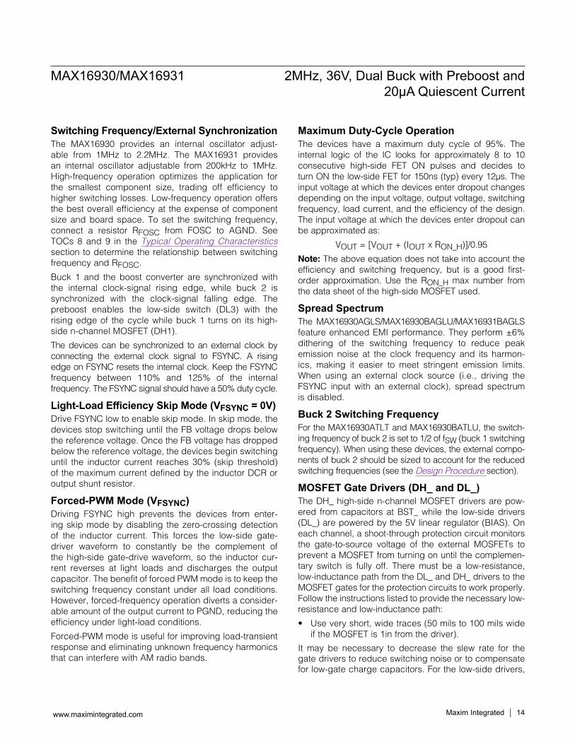
Current-Sense MeasurementFor the best current-sense accuracy and overcur-rent protection, use a ±1% tolerance current-sense resistor between the inductor and output as shown in Figure 1A. This configuration constantly monitors the inductor current, allowing accurate current-limit pro-tection. Use low-inductance current-sense resistors for accurate measurement.
Alternatively, high-power applications that do not require highly accurate current-limit protection can reduce the overall power dissipation by connecting a series RC circuit across the inductor (Figure 1B) with an equivalent time constant:
= + CSHL DCR
R2R R
R1 R2
and:
= +
DCREQ
L 1 1R
C R1 R2
where RCSHL is the required current-sense resistor and RDCR is the inductor’s series DC resistor. Use the induc-tance and RDCR values provided by the inductor manufacturer.
Carefully observe the PCB layout guidelines to ensure the noise and DC errors do no corrupt the differential current-sense signals seen by CS_ and OUT_. Place the sense resistor close to the devices with short, direct traces, making a Kelvin-sense connection to the current-sense resistor.
Input Capacitor in Buck ConvertersThe discontinuous input current of the buck converter causes large input ripple currents and therefore the input capacitor must be carefully chosen to withstand the input ripple current and keep the input voltage ripple within design requirements. The 180° ripple phase operation increases the frequency of the input capacitor ripple current to twice the individual converter switching frequency. When using ripple phasing, the worst-case input capacitor ripple current is when the converter with the highest output current is on.
The input voltage ripple is composed of DVQ (caused by the capacitor discharge) and DVESR (caused by the ESR of the input capacitor). The total voltage ripple is the sum of DVQ and DVESR that peaks at the end of an on-cycle.
MAX16930/MAX16931 2MHz, 36V, Dual Buck with Preboost and 20µA Quiescent Current
www.maximintegrated.com Maxim Integrated 18
Calculate the input capacitance and ESR required for a specific ripple using the following equation:
( )
ESR
P PLOAD(MAX)
OUTLOAD(MAX)
ININ
Q SW
VESR[ ]
II
2
VI x
VC [µF]
V x f
−
∆W =
∆ +
=
∆
where:
( )−
−∆ = IN OUT OUT
P PIN SW
V V x VI
V x f x L
ILOAD(MAX) is the maximum output current in A, DIP-P is the peak-to-peak inductor current in A, fSW is the switch-ing frequency in MHz, and L is the inductor value in µH.
The internal 5V linear regulator (BIAS) includes an output UVLO with hysteresis to avoid unintentional chattering during turn-on. Use additional bulk capacitance if the input source impedance is high. At lower input voltage, additional input capacitance helps avoid possible under-shoot below the undervoltage lockout threshold during transient loading.
Figure 1. Current-Sense Configurartions
MAX16930/MAX16931 2MHz, 36V, Dual Buck with Preboost and 20µA Quiescent Current
www.maximintegrated.com Maxim Integrated 19
COUT
COUT
CIN
CIN
L
NL
NH
INPUT (VIN)
A) OUTPUT SERIES RESISTOR SENSING
DH_
LX_
DL_
GND
CS_
OUT_
L
NL
NH
R2
CEQ
DCR
R1
INPUT (VIN)
B) LOSSLESS INDUCTOR SENSING
DH_
LX_
DL_
GND
CS_
OUT_
INDUCTOR
RCSHL = ( )RDCRR2
R1 + R2
RDCR = [ + ]1R1
1R2
LCEQ
MAX16930/MAX16931
MAX16930/MAX16931
RSENSE

Output Capacitor in Buck ConvertersThe actual capacitance value required relates to the physical size needed to achieve low ESR, as well as to the chemistry of the capacitor technology. The capacitor is usually selected by ESR and the voltage rating rather than by capacitance value.
When using low-capacity filter capacitors, such as ceramic capacitors, size is usually determined by the capacity needed to prevent VSAG and VSOAR from causing problems during load transients. Generally, once enough capacitance is added to meet the over-shoot requirement, undershoot at the rising load edge is no longer a problem (see the Transient Considerations section). However, low-capacity filter capacitors typically have high-ESR zeros that can affect the overall stability.
The total voltage sag (VSAG) can be calculated as follows:
∆=
× −
∆ − ∆+
2LOAD(MAX)
SAGOUT IN MAX OUT
LOAD(MAX)
OUT
L( I )V
2C ((V D ) V )
I (t t)
C
The amount of overshoot (VSOAR) during a full-load to no-load transient due to stored inductor energy can be calculated as:
∆≈
2LOAD(MAX)
SOAROUT OUT
( I ) LV
2C V
ESR ConsiderationsThe output filter capacitor must have low enough equivalent series resistance (ESR) to meet output ripple and load-transient requirements, yet have high enough ESR to satisfy stability requirements. When using high-capacitance, low-ESR capacitors, the filter capacitor’s ESR dominates the output-voltage ripple. So the output capacitor’s size depends on the maximum ESR required to meet the output-voltage ripple (VRIPPLE(P-P)) specifications:
− =RIPPLE(P P) LOAD(MAX)V ESR xI x LIR
In standby mode, the inductor current becomes discon-tinuous, with peak currents set by the idle-mode current-sense threshold (VCS,SKIP = 26mV (typ)).
Transient ConsiderationsThe output capacitor must be large enough to absorb the inductor energy while transitioning from no-load to full-load condition without tripping the overvoltage fault
protection. The total output-voltage sag is the sum of the voltage sag while the inductor is ramping up and the voltage sag before the next pulse can occur. Therefore:
( )
( )
∆=
−
∆ − ∆+
2LOAD(MAX)
OUTSAG IN MAX OUT
LOAD(MAX)
SAG
L IC
2V (V x D V )
I t t
V
where DMAX is the maximum duty factor (approximately 95%), L is the inductor value in µH, COUT is the output capacitor value in µF, t is the switching period (1/fSW) in µs, and Dt equals (VOUT/VIN) x t.
The MAX16930/MAX16931 use a current-mode control scheme that regulates the output voltage by forcing the required current through the external inductor, so the controller uses the voltage drop across the DC resistance of the inductor or the alternate series current-sense resistor to measure the inductor current. Current-mode control eliminates the double pole in the feedback loop caused by the inductor and output capacitor result-ing in a smaller phase shift and requiring less elaborate error-amplifier compensation than voltage-mode control. A single series resistor (RC) and capacitor (CC) is all that is required to have a stable, high-bandwidth loop in applications where ceramic capacitors are used for out-put filtering (see Figure 2). For other types of capacitors, due to the higher capacitance and ESR, the frequency of the zero created by the capacitance and ESR is lower than the desired closed-loop crossover frequency. To stabilize a nonceramic output capacitor loop, add another compensation capacitor (CF) from COMP to AGND to cancel this ESR zero.
The basic regulator loop is modeled as a power modulator, output feedback divider, and an error amplifier as shown in Figure 2. The power modulator has a DC gain set by gmc x RLOAD, with a pole and zero pair set by RLOAD, the output capacitor (COUT), and its ESR. The loop response is set by the following equations:
MOD(dc) mc LOADGAIN g R= ×
where RLOAD = VOUT/ILOUT(MAX) in I and gmc = 1/(AV_CS x RDC) in S. AV_CS is the voltage gain of the current-sense amplifier and is typically 11V/V. RDC is the DC resistance of the inductor or the current-sense resistor in I.
MAX16930/MAX16931 2MHz, 36V, Dual Buck with Preboost and 20µA Quiescent Current
www.maximintegrated.com Maxim Integrated 20

In a current-mode step-down converter, the output capac-itor and the load resistance introduce a pole at the follow-ing frequency:
pMODOUT LOAD
1f
2 C R=
π × ×
The unity gain frequency of the power stage is set by COUT and gmc:
mcUGAINpMOD
OUT
gf
2 C=
π ×The output capacitor and its ESR also introduce a zero at:
zMODOUT
1f
2 ESR C=
π × ×
When COUT is composed of “n” identical capacitors in parallel, the resulting COUT = n x COUT(EACH), and ESR = ESR(EACH)/n. Note that the capacitor zero for a parallel combination of alike capacitors is the same as for an indi-vidual capacitor.
The feedback voltage-divider has a gain of GAINFB = VFB/VOUT, where VFB is 1V (typ).
The transconductance error amplifier has a DC gain of GAINEA(DC) = gm,EA x ROUT,EA, where gm,EA is the error amplifier transconductance, which is 1200µS (typ), and ROUT,EA is the output resistance of the error amplifier, which is 30MI (typ) (see the Electrical Characteristics table.)
A dominant pole (fdpEA) is set by the compensation capacitor (CC) and the amplifier output resistance (ROUT,EA). A zero (fZEA) is set by the compensation resistor (RC) and the compensation capacitor (CC). There is an optional pole (fPEA) set by CF and RC to cancel the output capacitor ESR zero if it occurs near the crossover frequency (fC), where the loop gain equals 1 (0dB)). Thus:
=π × × +dpEA
C OUT,EA C
1f
2 C (R R )
zEAC C
1f
2 C R=
π × ×
pEAF C
1f
2 C R=
π × ×
The loop-gain crossover frequency (fC) should be set below 1/5th of the switching frequency and much higher than the power-modulator pole (fpMOD). Select a value for fC in the range:
<< ≤ SWpMOD C
ff f
5
At the crossover frequency, the total loop gain must be equal to 1. So:
C CFB
MOD(f ) EA(f )OUT
VGAIN GAIN 1
V× × =
CEA(f ) m,EA CGAIN g R= ×
CpMOD
MOD(f ) MOD(dc)C
fGAIN GAIN
f= ×
Therefore:
CFB
MOD(f ) m,EA COUT
VGAIN g R 1
V× × × =
Solving for RC:
C
OUTC
m,EA FB MOD(f )
VR
g V GAIN=
× ×
Figure 2. Compensation Network
MAX16930/MAX16931 2MHz, 36V, Dual Buck with Preboost and 20µA Quiescent Current
www.maximintegrated.com Maxim Integrated 21
CS_
OUT_
FB_
R1
RESR
CC
CF
RC
R2
VREF
COUT
gmc = 1/(AVCS x RDC)
CURRENT-MODEPOWER
MODULATION
ERRORAMP
COMP_
gmea = 1200µS
30MI

Set the error-amplifier compensation zero formed by RC and CC at the fpMOD. Calculate the value of CC as follows:
C1
C2 f RpMOD C
=π × ×
If fzMOD is less than 5 x fC, add a second capacitor CF from COMP to AGND. The value of CF is:
F1
C2 f RzMOD C
=π × ×
As the load current decreases, the modulator pole also decreases; however, the modulator gain increases accordingly and the crossover frequency remains the same.
Below is a numerical example to calculate the compensation network component values of Figure 2:
AV_CS = 11V/V
RDCR = 15mI
gmc = 1/(AV_CS x RDC) = 1/(11 x 0.015) = 6.06
VOUT = 5V
IOUT(MAX) = 5.33A
RLOAD = VOUT/IOUT(MAX) = 5V/5.33A = 0.9375I
COUT = 2x47µF = 94µF
ESR = 9mI/2 = 4.5mI
fSW = 26.4/65.5kI = 0.403MHz
= × =MOD(dc)GAIN 6.06 0.9375 5.68
pMOD1
f 1.8kHz2 94µF 0.9375
= ≈π × ×
<< ≤ SWpMOD C
ff f
5
C1.8kHz f 80.6kHz<< ≤
select fC = 40kHz
zMOD1
f 376kHz2 4.5m 94µF
= ≈π × W ×
since fzMOD > fC:RC ≈ 16kI
CC ≈ 5.6nF
CF ≈ 27pF
Boost Converter Design Procedure Setting the Output Voltage in Boost ConverterAdjust the boost converter output voltage by connecting a resistive divider from the output of the boost converter to FBBST to TERM (Figure 3) and RB2 (FB3 to TERM resistor). Calculate RB1 (VOUT(BOOST) to FBBST resistor) using the following equation:
= −
)OUT(BOOSTB1 B2
FB3
VR R 1
V
where VFB3 = 1.2V (typ) (see the Electrical Characteristics table).
Inductor Selection in Boost ConverterDuty cycle and frequency are important to calculate the inductor size, as the inductor current ramps up during the on-time of the switch and ramps down during its off-time. A higher switching frequency generally improves transient response and reduces component size.
However, if the boost components are to be used as the input filter components during nonboost operation, a low frequency is advantageous.
The boost frequency is selected as a multiple of the buck frequency by setting the input voltage of FSELBST.
• If VFSELBST =VGND, then fBOOST = fSW
• If VFSELBST = VBIAS, then fBOOST = 1/5fSW
Figure 3. Boost Converter Adjustable Output Voltage
MAX16930/MAX16931 2MHz, 36V, Dual Buck with Preboost and 20µA Quiescent Current
www.maximintegrated.com Maxim Integrated 22
RB1
RB2
VOUT(BOOST)
TERM
FB3
MAX16930/MAX16931

The duty-cycle range of the boost converter depends on the effective input to output-voltage ratio. In the following calculations, the duty cycle refers to the on-time of the boost MOSFET:
−=
OUT(MAX) BAT(MIN)MAX
OUT(MAX)
V VD
V
or including the voltage drops across the inductor, MOSFET (VON,FET), and the boost diode (VD):
− + +=
OUT(MAX) BAT(MIN) D OUT DCMAX
OUT(MAX)
V V V (I xR )D
V
In some applications, it may be beneficial to maintain discontinuous conduction (DCM) in the boost converter under all conditions. This formula defines the maximum size of the inductor for DCM mode:
LMAX < VIN(MIN) x DMAX/(2 x (IOUT(MAX)/1 - DMAX)) x fSW(MIN)
The ratio of the inductor peak-to-peak AC current to DC average current (LIR) must be selected first. A good initial value is a 30% peak-to-peak ripple current to average-current ratio (LIR = 0.3). The switching frequency, input voltage, output voltage, and selected LIR determine the inductor value as follows:
×=
×IN
SW
V DL[µH]
f [MHz] LIR
where:
D = (VOUT - VIN)/VOUT VIN = Typical input voltage VOUT = Typical output voltage
LIR = 0.3 x IOUT/1 - D
Select the inductor with a saturation current rating higher than the peak switch current limit of the converter:
∆> +
L,RIP,MAXL,PEAK L,MAX
II I
2
Running a boost converter in continuous conduction mode introduces a right-half plane zero into the transfer func-tion, which can only be compensated by reducing band-width in the voltage feedback loop by adding a capacitor across the low-side feedback resistor. This results in a system that is slow to respond to load and line changes.
If the boost converter response is too slow, increase the ripple current. A smaller inductor and higher frequency generally improves the preboost, especially for high input to output ratios.
MOSFET Selection in Boost ConverterThe key selection parameters to choose the n-channel MOSFET used in the boost converter are as follows.
Threshold VoltageThe boost n-channel MOSFETs must be a logic-level type with guaranteed on-resistance specifications at VGS = 4.5V.
Maximum Drain-to-Source Voltage (VDS(MAX))The MOSFET must be chosen with an appropriate VDS rating to handle all VIN voltage conditions.
Current CapabilityThe n-channel MOSFET must deliver the input current (IIN(MAX)):
=−
MAXIN(MAX) LOAD(MAX)
MAX
DI I x
1 D
Choose MOSFETs with the appropriate average current at VGS = 4.5V.
Diode Selection in Boost ConverterThe diode must deliver the average output current (IOUT) plus the peak inductor current (ILPEAK). The boost diode current can be higher during nonboost operation when it supplies current to both buck converters under full-load conditions.
Use a boost diode with a power dissipation of P = IOUT x VDIODE or higher. To reduce the power dissipation, use a Schottky diode.
Input Capacitor Selection in Boost ConverterThe input current for the boost converter is continuous and the RMS ripple current at the input capacitor is low. Calculate the minimum input capacitor value and maxi-mum ESR using the following equations:
∆=
∆
∆=
∆
LBAT
SW Q
ESR
L
I x DC
4 x f x V
VESR
I
MAX16930/MAX16931 2MHz, 36V, Dual Buck with Preboost and 20µA Quiescent Current
www.maximintegrated.com Maxim Integrated 23

where:
−∆ = BAT DS
LSW
(V V ) x DI
L x f
VDS is the total voltage drop across the external MOSFET plus the voltage drop across the inductor ESR. DIL is peak-to-peak inductor ripple current as calculated above. DVQ is the portion of input ripple due to the capacitor discharge and DVESR is the contribution due to ESR of the capacitor. Assume the input capacitor ripple contri-bution due to ESR (DVESR) and capacitor discharge (DVQ) are equal when using a combination of ceramic and aluminum capacitors. During the converter turn-on, a large current is drawn from the input source especially at high output-to-input differential.
Output Capacitor Selection in Boost ConverterIn a boost converter, the output capacitor supplies the load current when the boost MOSFET is on. The required output capacitance is high, especially at higher duty cycles. Also, the output capacitor ESR needs to be low enough to minimize the voltage drop while supporting the load current. Use the following equations to calculate the output capacitor for a specified output ripple. All ripple values are peak-to-peak.
∆=
=∆
ESR
OUT
OUT MAXOUT
Q SW
VESR
I
I x DC
V x f
IOUT is the load current in A, fSW is in MHz, COUT is µF, DVQ is the portion of the ripple due to the capacitor discharge, and DVESR is the contribution due to the ESR of the capacitor. DMAX is the maximum duty cycle at the minimum input voltage. Use a combination of low-ESR ceramic and high-value, low-cost aluminum capacitors for lower output ripple and noise.
Shunt Resistor Selection in Boost ConverterThe current-sense resistor (RCS), connected between the battery and the inductor, sets the current limit. The CS input has a voltage trip level (VCS) of 120mV (typ).
Set the current-limit threshold high enough to accommodate the component variations. Use the follow-ing equation to calculate the value of RCS:
= CSCS
IN(MAX)
VR
I
where IIN(MAX) is the peak current that flows through the MOSFET at full load and minimum VIN.
IIN(MAX) = ILOAD(MAX) /(1 - DMAX)
When the voltage produced by this current (through the current-sense resistor) exceeds the current-limit comparator threshold, the MOSFET driver (DL3) quickly terminates the on-cycle.
MAX16930/MAX16931 2MHz, 36V, Dual Buck with Preboost and 20µA Quiescent Current
www.maximintegrated.com Maxim Integrated 24
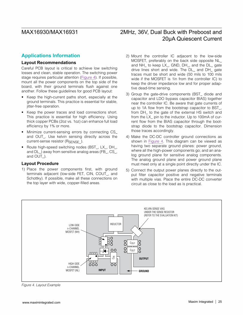
Applications InformationLayout RecommendationsCareful PCB layout is critical to achieve low switching losses and clean, stable operation. The switching power stage requires particular attention (Figure 4). If possible, mount all the power components on the top side of the board, with their ground terminals flush against one another. Follow these guidelines for good PCB layout:
• Keep the high-current paths short, especially at the ground terminals. This practice is essential for stable, jitter-free operation.
• Keep the power traces and load connections short. This practice is essential for high efficiency. Using thick copper PCBs (2oz vs. 1oz) can enhance full load efficiency by 1% or more.
• Minimize current-sensing errors by connecting CS_ and OUT_. Use kelvin sensing directly across the current-sense resistor (RSENSE_).
• Route high-speed switching nodes (BST_, LX_, DH_, and DL_) away from sensitive analog areas (FB_, CS_, and OUT_).
Layout Procedure1) Place the power components first, with ground
terminals adjacent (low-side FET, CIN, COUT_, and Schottky). If possible, make all these connections on the top layer with wide, copper-filled areas.
2) Mount the controller IC adjacent to the low-side MOSFET, preferably on the back side opposite NL_ and NH_ to keep LX_, GND, DH_, and the DL_ gate drive lines short and wide. The DL_ and DH_ gate traces must be short and wide (50 mils to 100 mils wide if the MOSFET is 1in from the controller IC) to keep the driver impedance low and for proper adap-tive dead-time sensing.
3) Group the gate-drive components (BST_ diode and capacitor and LDO bypass capacitor BIAS) together near the controller IC. Be aware that gate currents of up to 1A flow from the bootstrap capacitor to BST_, from DH_ to the gate of the external HS switch and from the LX_ pin to the inductor. Up to 100mA of cur-rent flow from the BIAS capacitor through the boot-strap diode to the bootstrap capacitor. Dimension those traces accordingly.
4) Make the DC-DC controller ground connections as shown in Figure 4. This diagram can be viewed as having two separate ground planes: power ground, where all the high-power components go; and an ana-log ground plane for sensitive analog components. The analog ground plane and power ground plane must meet only at a single point directly under the IC.
5) Connect the output power planes directly to the out-put filter capacitor positive and negative terminals with multiple vias. Place the entire DC-DC converter circuit as close to the load as is practical.
Figure 4. Layout Example
MAX16930/MAX16931 2MHz, 36V, Dual Buck with Preboost and 20µA Quiescent Current
www.maximintegrated.com Maxim Integrated 25
INDUCTOR
COUT
COUT
C IN
INPUT
KELVIN-SENSE VIASUNDER THE SENSE RESISTOR(REFER TO THE EVALUATION KIT)
GROUND
OUTPUT
LOW-SIDEn-CHANNEL
MOSFET (NH)
HIGH-SIDEn-CHANNEL
MOSFET (NL)

Block Diagram
MAX16930/MAX16931 2MHz, 36V, Dual Buck with Preboost and 20µA Quiescent Current
www.maximintegrated.com Maxim Integrated 26
EAMP1
PGOODCOMP
PGOOD1 COMP1
PGOOD LOW LEVEL
PGOOD HIGH LEVEL
FB1
OUT1
CS1
EN1
80 mV(TYP) MAXDIFFERENTIAL INPUT
CS3P
BSTON
CS3N
FB3
TERM
50 mV(TYP) MAXDIFFERENT INPUT
FEEDBACKSELECT LOGIC
REF = 1V
CURRENT LIMITTHRESHOLD
OSCILLATOR
TIED HIGH (PWM MODE)
TIED LOW (SKIP MODE)
CLK2
VIN
CLK1
INTERNALSOFT START
SLOPECOMP LOGIC
CLK 180°OUT OF PHASE
INTERNAL LINEARREGULATOR
SWITCHOVER
SLOPE COMPLOGIC
DC-DC3CONTROL LOGIC
DC-DC1CONTROL LOGIC
BOOST ENFLAG
ZEROCROSSCOMP
CSA1
CSA3
REF3 = 1.25V
EN3
EP
EAMP3
PWM3
CL
CURRENT LIMITTHRESHOLD
LOW GAIN EAMP, NOCOMP PIN REQUIRED
CL3
PWM1
LX1
LX2
LX1
BIAS
CLK1STEP-DOWN DC-DC1
GATE DRIVELOGIC
EN1 BST1
DH1
LX1
DL1
PGND1
PGND2
BIAS
EXTVCCIF 3.1V <
VEXTVCC < 5.2V
PWM1
ZX1
SPREAD SPECTRUMOPTION AVAILABLE WITHINTERNAL CLOCK ONLY
EXTERNALCLOCK INPUT
FSYNCSELECT LOGIC
DC-DC2 CONTROL LOGICSAME AS DC-DC1 ABOVE
FSYNC
FOSC
COMP2
INS
FB2
OUT2
CS2
EN2
PGOOD2
AGND
CLK2STEP-DOWN DC-DC2
GATE DRIVELOGIC
EN2 BST2
DH2
LX2
DL2
PWM2
ZX2
LX2
IN
VIN STEP-UP DC-DC3
GATE DRIVELOGIC
BOOSTENABLED PGND3
DL3
BIAS
PWM3
CLK3
EN3 EN GOESHIGH
CHECK FOR INSTHRESHOLDS
BOOSTENABLED
CLK3
CLK1
IF LOW, CLK3 = CLK1
IF HIGH, CLK3 = CLK1/5
FSELBST FSELBSTINPUT
TIED LOW
TIED HIGH
PRE-BST SNSTHRESHOLD
COMPARATOR
START-UP TURNON THRESHOLD
BOOST ON-OFFTHRESHOLDS
UVLO THRESHOLD
MAX16930

Typical Operating Circuit
MAX16930/MAX16931 2MHz, 36V, Dual Buck with Preboost and 20µA Quiescent Current
www.maximintegrated.com Maxim Integrated 27
MAX16930MAX16931
IN
TERM
IN
IN
OUT2
TERM
VBAT
BIAS
PGND
1 IN
FB3
PGND
3
EN3
INS
IN
TERM
CS3P
CS3N
DL3EN1
DL1
BST1
LX1
DH1
PGOOD1
RPGOOD1
COMP1
FB1
CS1
OUT1
FSELBST
BSTON
N.C.
PGND2
BST2
LX2
DH2
EN2
PGOO
D2
EXTV
CC
FB2
CS2
OUT2
COM
P2
N.C.
FSYN
C
AGND
FOSC
OUT1 BIAS
BIAS
BIAS
DL2
OUT1

Selector Guide
MAX16930/MAX16931 2MHz, 36V, Dual Buck with Preboost and 20µA Quiescent Current
www.maximintegrated.com Maxim Integrated 28
PARTBUCK 1 SWITCHING FREQUENCY (fSW1)
BUCK 2 SWITCHING FREQUENCY (fSW2)
SPREAD SPECTRUM (%)
INS ACTIVE
MAX16930AGLC/VY+* 1MHz to 2.2MHz fSW1 — Active
MAX16930AGLR/VY+ 1MHz to 2.2MHz fSW1 — Active
MAX16930ATLR/V+ 1MHz to 2.2MHz fSW1 — Active
MAX16930ATLT/V+ 1MHz to 2.2MHz 1/2fSW1 — Active
MAX16930ATLV/V+ 1MHz to 2.2MHz fSW1 — Inactive
MAX16930BAGLD/VY+* 1MHz to 2.2MHz fSW1 6 Active
MAX16930BAGLS/VY+ 1MHz to 2.2MHz fSW1 6 Active
MAX16930BATLS/V+ 1MHz to 2.2MHz fSW1 6 Active
MAX16930BATLU/V+ 1MHz to 2.2MHz 1/2fSW1 6 Active
MAX16930BATLW/V+ 1MHz to 2.2MHz fSW1 6 Inactive
MAX16931ATLR/V+ 200kHz to 1MHz fSW1 — Active
MAX16931BATLS/V+ 200kHz to 1MHz fSW1 6 Active
*Future product—contact factory for availability.

Ordering Information
Note: Insert the desired suffix letter (from Selector Guide) into the blank to indicate buck 2 switching frequency and spread spectrum. /V denotes an automotive qualified part.+Denotes a lead(Pb)-free/RoHS-compliant package.*Future product—contact factory for availability.**Exposed pad.†Exposed pad side-wettable flanked package.
Package InformationFor the latest package outline information and land patterns (foot-prints), go to www.maximintegrated.com/packages. Note that a “+”, “#”, or “-” in the package code indicates RoHS status only. Package drawings may show a different suffix character, but the drawing pertains to the package regardless of RoHS status.
Chip InformationPROCESS: BiCMOS
MAX16930/MAX16931 2MHz, 36V, Dual Buck with Preboost and 20µA Quiescent Current
www.maximintegrated.com Maxim Integrated 29
PARTTEMP
RANGEPIN-PACKAGE
MAX16930AGL_/VY+-40°C to +125°C
40 QFND-EP†
MAX16930ATL_/V+-40°C to +125°C
40 TQFN-EP**
MAX16930BAGL_/VY+-40°C to +125°C
40 QFND-EP†
MAX16930BATL_/V+-40°C to +125°C
40 TQFN-EP**
MAX16931AGL_/VY+*-40°C to +125°C
40 QFND-EP**
MAX16931ATL_/V+-40°C to +125°C
40 TQFN-EP**
MAX16931BAGL_/VY+*-40°C to +125°C
40 QFND-EP**
MAX16931BATL_/V+-40°C to +125°C
40 TQFN-EP**
PACKAGETYPE
PACKAGECODE
OUTLINENO.
LANDPATTERN NO.
40 TQFN-EP T4066+5 21-0141 90-0055
40 QFND-EP G4066Y+1 21-0564 90-0362

Revision History
Maxim Integrated cannot assume responsibility for use of any circuitry other than circuitry entirely embodied in a Maxim Integrated product. No circuit patent licenses are implied. Maxim Integrated reserves the right to change the circuitry and specifications without notice at any time. The parametric values (min and max limits) shown in the Electrical Characteristics table are guaranteed. Other parametric values quoted in this data sheet are provided for guidance.
Maxim Integrated and the Maxim Integrated logo are trademarks of Maxim Integrated Products, Inc.
MAX16930/MAX16931 2MHz, 36V, Dual Buck with Preboost and 20µA Quiescent Current
© 2016 Maxim Integrated Products, Inc. 30
REVISION NUMBER
REVISION DATE
DESCRIPTIONPAGES
CHANGED
0 3/13 Initial release —
1 7/13Changed Supply Monitor section resistor value, updated inductor selection in Boost Converter section, and updated land pattern number in Package Information
15, 23, 28
2 8/13 Removed future product asterisk from MAX16931 28
3 12/13Added side-wettable part to data sheet, updated thermal information for TQFN, and updated exposed pad package info updated
1, 2, 10, 28
4 4/14Added latchup information about the RPGOOD1 resistor to the PGOOD1 Pin Description, Voltage Monitoring (PGOOD_) section, Preboost section, and Typical Operating Circuit; added the Maximum Duty-Cycle Operation section
11, 14–16, 27
5 6/14
Added new parts and also clarified feedback/output/GND connection information; updated Electrical Characteristics, Pin Description, Supply Monitoring (INS), Setting the Output Voltage in Buck Converters, Typical Operating Circuit, and Selector Guide sections
4, 5, 11, 16, 17, 27, 28
6 7/14 Removed future product designations from Selector Guide 28
7 1/15 Updated Benefits and Features section 1
8 3/15Added new Note 1 to Absolute Maximum Ratings section and renumbered the remaining notes in Package Thermal Characteristics and Electrical Characteristics sections
2–5
9 5/15Added MAX16930AGLC/VY+ and MAX16930AGLD/VY+ to Selector Guide and removed future product designations from Ordering Information
28
10 2/16Updated Selector Guide and added MAX16930BATL_/V+, MAX16930BAGL_/VY+, MAX16931BATL_/V+, and MAX16931BAGL_/VY+ to Ordering Information
28, 29
11 4/16Updated part numbers with B variation, updated TOCs 29–31, Selector Guide, changing MAX16930AGLD/VY+* to MAX16930BAGLD/VY+*, and deleting MAX16930BATLR/V+
3–5, 9, 11, 14, 16, 28
12 4/16 Added future product designation to two listings in Ordering Information 29
13 7/16 Added MAX16930AGLR/VY+ and MAX16930BAGLS/VY+ to Selector Guide 28