Embed Size (px)
Citation preview
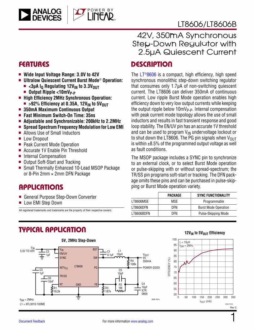
LT8606/LT8606B
1Rev C
For more information www.analog.com
FEATURES
TYPICAL APPLICATION
DESCRIPTION
42V, 350mA Synchronous Step-Down Regulator with
2.5µA Quiescent Current
The LT®8606 is a compact, high efficiency, high speed synchronous monolithic step-down switching regulator that consumes only 1.7µA of non-switching quiescent current. The LT8606 can deliver 350mA of continuous current. Low ripple Burst Mode operation enables high efficiency down to very low output currents while keeping the output ripple below 10mVP-P. Internal compensation with peak current mode topology allows the use of small inductors and results in fast transient response and good loop stability. The EN/UV pin has an accurate 1V threshold and can be used to program VIN undervoltage lockout or to shut down the LT8606. The PG pin signals when VOUT is within ±8.5% of the programmed output voltage as well as fault conditions.
The MSOP package includes a SYNC pin to synchronize to an external clock, or to select Burst Mode operation or pulse-skipping with or without spread-spectrum; the TR/SS pin programs soft-start or tracking. The DFN pack-age omits these pins and can be purchased in pulse-skip-ping or Burst Mode operation variety.APPLICATIONS
n Wide Input Voltage Range: 3.0V to 42V n Ultralow Quiescent Current Burst Mode® Operation:
n <3µA IQ Regulating 12VIN to 3.3VOUT n Output Ripple <10mVP-P
n High Efficiency 2MHz Synchronous Operation: n >92% Efficiency at 0.35A, 12VIN to 5VOUT
n 350mA Maximum Continuous Output n Fast Minimum Switch-On Time: 35ns n Adjustable and Synchronizable: 200kHz to 2.2MHz n Spread Spectrum Frequency Modulation for Low EMI n Allows Use of Small Inductors n Low Dropout n Peak Current Mode Operation n Accurate 1V Enable Pin Threshold n Internal Compensation n Output Soft-Start and Tracking n Small Thermally Enhanced 10-Lead MSOP Package
or 8-Pin 2mm × 2mm DFN Package
n General Purpose Step-Down Converter n Low EMI Step Down
All registered trademarks and trademarks are the property of their respective owners.
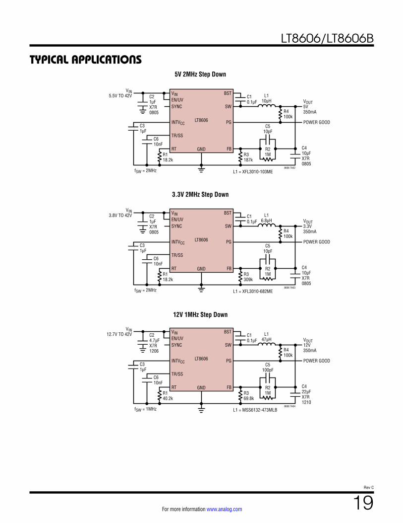
5V, 2MHz Step-Down
12VIN to 5VOUT Efficiency
VIN BSTEN/UV
C10.1µF
C510pF
R21M
C21µF
VIN5.5V TO 42V
C610nF
C31µF
VOUT5V350mA
POWER GOOD
R3187k
8606 TA01a
L110µH
SYNC
INTVCC
TR/SS
RT
LT8606
GND
SW
PG
FB
R4100k
R118.2k
L1 = XFL3010-103ME
C410µFX7R0805
fSW = 2MHz
fSW = 2MHzL = 10µH
IOUT (mA)0 50 100 150 200 250 300 350
50
55
60
65
70
75
80
85
90
95
100
EFFI
CIEN
CY (%
)
8606 TA01b
PACKAGE SYNC FUNCTIONALITY
LT8606MSE MSE Programmable
LT8606DFN DFN Burst Mode Operation
LT8606BDFN DFN Pulse-Skipping Mode
Document Feedback
LT8606/LT8606B
2Rev C
For more information www.analog.com
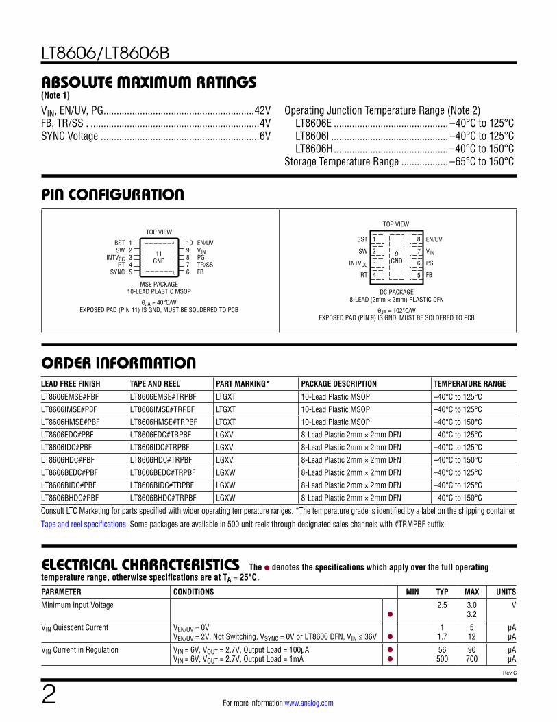
PIN CONFIGURATION
ABSOLUTE MAXIMUM RATINGS
VIN, EN/UV, PG ..........................................................42VFB, TR/SS . .................................................................4VSYNC Voltage . ............................................................6V
(Note 1)
12345
BSTSW
INTVCCRT
SYNC
109876
EN/UVVINPGTR/SSFB
TOP VIEW
11GND
MSE PACKAGE10-LEAD PLASTIC MSOP
θJA = 40°C/WEXPOSED PAD (PIN 11) IS GND, MUST BE SOLDERED TO PCB
TOP VIEW
BST
SW
INTVCC
RT
EN/UV
VIN
PG
FB
DC PACKAGE8-LEAD (2mm × 2mm) PLASTIC DFN
θJA = 102°C/WEXPOSED PAD (PIN 9) IS GND, MUST BE SOLDERED TO PCB
9GND
4
1
2
3 6
5
7
8
ORDER INFORMATIONLEAD FREE FINISH TAPE AND REEL PART MARKING* PACKAGE DESCRIPTION TEMPERATURE RANGE
LT8606EMSE#PBF LT8606EMSE#TRPBF LTGXT 10-Lead Plastic MSOP –40°C to 125°CLT8606IMSE#PBF LT8606IMSE#TRPBF LTGXT 10-Lead Plastic MSOP –40°C to 125°CLT8606HMSE#PBF LT8606HMSE#TRPBF LTGXT 10-Lead Plastic MSOP –40°C to 150°CLT8606EDC#PBF LT8606EDC#TRPBF LGXV 8-Lead Plastic 2mm × 2mm DFN –40°C to 125°CLT8606IDC#PBF LT8606IDC#TRPBF LGXV 8-Lead Plastic 2mm × 2mm DFN –40°C to 125°CLT8606HDC#PBF LT8606HDC#TRPBF LGXV 8-Lead Plastic 2mm × 2mm DFN –40°C to 150°CLT8606BEDC#PBF LT8606BEDC#TRPBF LGXW 8-Lead Plastic 2mm × 2mm DFN –40°C to 125°CLT8606BIDC#PBF LT8606BIDC#TRPBF LGXW 8-Lead Plastic 2mm × 2mm DFN –40°C to 125°CLT8606BHDC#PBF LT8606BHDC#TRPBF LGXW 8-Lead Plastic 2mm × 2mm DFN –40°C to 150°C
Consult LTC Marketing for parts specified with wider operating temperature ranges. *The temperature grade is identified by a label on the shipping container.
Tape and reel specifications. Some packages are available in 500 unit reels through designated sales channels with #TRMPBF suffix.
The l denotes the specifications which apply over the full operating temperature range, otherwise specifications are at TA = 25°C.ELECTRICAL CHARACTERISTICS
Operating Junction Temperature Range (Note 2) LT8606E ............................................ –40°C to 125°C LT8606I ............................................. –40°C to 125°C LT8606H ............................................ –40°C to 150°CStorage Temperature Range .................. –65°C to 150°C
PARAMETER CONDITIONS MIN TYP MAX UNITS
Minimum Input Voltage
l
2.5 3.0 3.2
V
VIN Quiescent Current VEN/UV = 0V VEN/UV = 2V, Not Switching, VSYNC = 0V or LT8606 DFN, VIN ≤ 36V
l
1 1.7
5 12
µA µA
VIN Current in Regulation VIN = 6V, VOUT = 2.7V, Output Load = 100µA VIN = 6V, VOUT = 2.7V, Output Load = 1mA
l
l
56 500
90 700
µA µA
LT8606/LT8606B
3Rev C
For more information www.analog.com
The l denotes the specifications which apply over the full operating temperature range, otherwise specifications are at TA = 25°C.
Note 1: Stresses beyond those listed under Absolute Maximum Ratings may cause permanent damage to the device. Exposure to any Absolute Maximum Rating condition for extended periods may affect device reliability and lifetime. Absolute Maximum Ratings are those values beyond which the life of a device may be impaired.Note 2: The LT8606E is guaranteed to meet performance specifications from 0°C to 125°C junction temperature. Specifications over the –40°C to 125°C operating junction temperature range are assured by design, characterization, and correlation with statistical process controls. The LT8606I is guaranteed over the full –40°C to 125°C operating junction
temperature range. The LT8606H is guaranteed over the full –40°C to 150°C operating junction temperature range. High junction temperatures degrade operating lifetimes. Operating lifetime is derated at junction temperatures greater than 125°C.Note 3: This IC includes overtemperature protection that is intended to protect the device during overload conditions. Junction temperature will exceed 150°C when overtemperature protection is active. Continuous operation above the specified maximum operating junction temperature will reduce lifetime.
PARAMETER CONDITIONS MIN TYP MAX UNITS
Feedback Reference Voltage MSOP Package VIN = 6V, ILOAD = 100mA VIN = 6V, ILOAD = 100mA
l
0.774 0.762
0.778 0.778
0.782 0.798
V V
DFN Package VIN = 6V, ILOAD = 100mA VIN = 6V, ILOAD = 100mA
l
0.771 0.753
0.778 0.778
0.785 0.803
V V
Feedback Voltage Line Regulation VIN = 4.0V to 40V l ±0.02 ±0.06 %/V
Feedback Pin Input Current VFB = 1V ±20 nA
Minimum On-Time ILOAD = 350mA, SYNC = 0V or LT8606 DFN ILOAD = 350mA, SYNC = 1.9V or LT8606B DFN
l
l
35 35
65 60
ns ns
Minimum Off Time ILOAD = 300mA l 93 130 ns
Oscillator Frequency MSOP Package RT = 221k, ILOAD = 250mA RT = 60.4k, ILOAD = 250mA RT = 18.2k, ILOAD = 250mA
l
l
l
155 640 1.90
200 700 2.00
245 760 2.10
kHz kHz
MHz
DFN Package RT = 221k, ILOAD = 250mA RT = 60.4k, ILOAD = 250mA RT = 18.2k, ILOAD = 250mA
l
l
l
140 610 1.85
200 700 2.00
260 790 2.15
kHz kHz
MHz
Top Power NMOS On-Resistance ILOAD = 250mA 375 mΩ
Top Power NMOS Current Limit MSOP Package l 0.65 0.9 1.15 A
DFN Package l 0.65 1.1 1.4 A
Bottom Power NMOS On-Resistance 240 mΩ
SW Leakage Current VIN = 36V 5 µA
EN/UV Pin Threshold EN/UV Rising l 0.99 1.05 1.11 V
EN/UV Pin Hysteresis 50 mV
EN/UV Pin Current VEN/UV = 2V ±20 nA
PG Upper Threshold Offset from VFB VFB Rising l 5.0 8.5 13.0 %
PG Lower Threshold Offset from VFB VFB Falling l 5.0 8.5 13.0 %
PG Hysteresis 0.5 %
PG Leakage VPG = 42V ±200 nA
PG Pull-Down Resistance VPG = 0.1V 550 1200 Ω
Sync Low Input Voltage MSOP Only l 0.4 0.9 V
Sync High Input Voltage INTVCC = 3.5V, MSOP Only l 2.7 3.2 V
TR/SS Source Current MSOP Only l 1 2 3 µA
TR/SS Pull-Down Resistance Fault Condition, TR/SS = 0.1V, MSOP Only 300 900 Ω
Spread Spectrum Modulation Frequency VSYNC = 3.3V, MSOP Only 0.5 3 6 kHz
ELECTRICAL CHARACTERISTICS
LT8606/LT8606B
4Rev C
For more information www.analog.com
FB Voltage Load Regulation
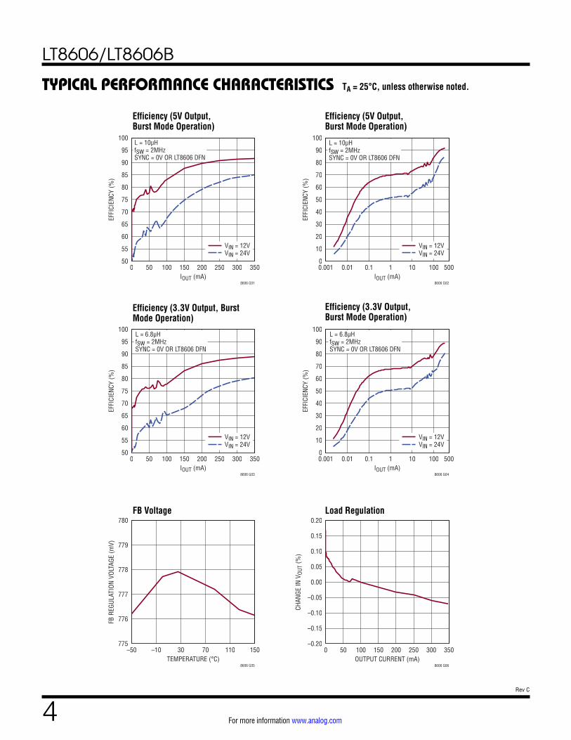
Efficiency (3.3V Output, Burst Mode Operation)
TYPICAL PERFORMANCE CHARACTERISTICS
Efficiency (5V Output, Burst Mode Operation)
Efficiency (5V Output, Burst Mode Operation)
Efficiency (3.3V Output, Burst Mode Operation)
IOUT (mA)0 50 100 150 200 250 300 350
50
55
60
65
70
75
80
85
90
95
100
EFFI
CIEN
CY (%
)
8606 G01
L = 10µHfSW = 2MHzSYNC = 0V OR LT8606 DFN
VIN = 12VVIN = 24V
IOUT (mA)0.001 0.01 0.1 1 10 100 5000
10
20
30
40
50
60
70
80
90
100
EFFI
CIEN
CY (%
)
8606 G02
VIN = 12VVIN = 24V
L = 10µHfSW = 2MHzSYNC = 0V OR LT8606 DFN
IOUT (mA)0 50 100 150 200 250 300 350
50
55
60
65
70
75
80
85
90
95
100
EFFI
CIEN
CY (%
)
8606 G03
VIN = 12VVIN = 24V
L = 6.8µHfSW = 2MHzSYNC = 0V OR LT8606 DFN
IOUT (mA)0.001 0.01 0.1 1 10 100 5000
10
20
30
40
50
60
70
80
90
100
EFFI
CIEN
CY (%
)
8606 G04
VIN = 12VVIN = 24V
L = 6.8µHfSW = 2MHzSYNC = 0V OR LT8606 DFN
TEMPERATURE (°C)–50 –10 30 70 110 150
775
776
777
778
779
780
FB R
EGUL
ATIO
N VO
LTAG
E (m
V)
8606 G05OUTPUT CURRENT (mA)
0 50 100 150 200 250 300 350–0.20
–0.15
–0.10
–0.05
0.00
0.05
0.10
0.15
0.20
CHAN
GE IN
VOU
T (%
)
8606 G06
TA = 25°C, unless otherwise noted.
LT8606/LT8606B
5Rev C
For more information www.analog.com
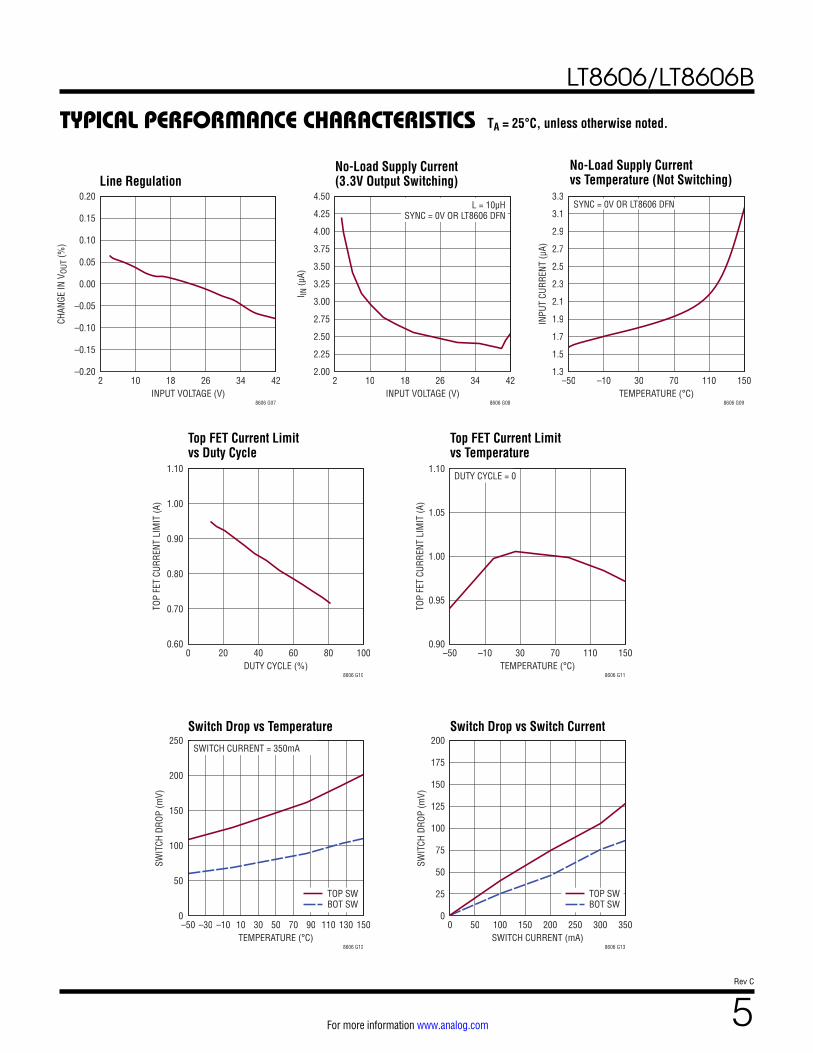
TYPICAL PERFORMANCE CHARACTERISTICS
Line RegulationNo-Load Supply Current (3.3V Output Switching)
No-Load Supply Current vs Temperature (Not Switching)
Top FET Current Limit vs Duty Cycle
Top FET Current Limit vs Temperature
Switch Drop vs Temperature Switch Drop vs Switch Current
INPUT VOLTAGE (V)2 10 18 26 34 42
–0.20
–0.15
–0.10
–0.05
0.00
0.05
0.10
0.15
0.20
CHAN
GE IN
VOU
T (%
)
8606 G07INPUT VOLTAGE (V)
2 10 18 26 34 422.00
2.25
2.50
2.75
3.00
3.25
3.50
3.75
4.00
4.25
4.50
I IN (µ
A)
8606 G08
L = 10µHSYNC = 0V OR LT8606 DFN
TEMPERATURE (°C)–50 –10 30 70 110 150
1.3
1.5
1.7
1.9
2.1
2.3
2.5
2.7
2.9
3.1
3.3
INPU
T CU
RREN
T (µ
A)
8606 G09
SYNC = 0V OR LT8606 DFN
DUTY CYCLE (%)0 20 40 60 80 100
0.60
0.70
0.80
0.90
1.00
1.10
TOP
FET
CURR
ENT
LIM
IT (A
)
8606 G10
DUTY CYCLE = 0
TEMPERATURE (°C)–50 –10 30 70 110 150
0.90
0.95
1.00
1.05
1.10
TOP
FET
CURR
ENT
LIM
IT (A
)
8606 G11
SWITCH CURRENT = 350mA
TEMPERATURE (°C)–50 –30 –10 10 30 50 70 90 110 130 150
0
50
100
150
200
250
SWIT
CH D
ROP
(mV)
8606 G12
TOP SWBOT SW
SWITCH CURRENT (mA)0 50 100 150 200 250 300 350
0
25
50
75
100
125
150
175
200
SWIT
CH D
ROP
(mV)
8606 G13
TOP SWBOT SW
TA = 25°C, unless otherwise noted.

LT8606/LT8606B
6Rev C
For more information www.analog.com
TYPICAL PERFORMANCE CHARACTERISTICS TA = 25°C, unless otherwise noted.
Minimum On-Time vs Temperature
Minimum Off-Time vs Temperature
Dropout Voltage vs Output CurrentSwitching Frequency vs Temperature
Burst Frequency vs Output Current
Minimum Load to Full Frequency (SYNC Float to 1.9V) (MSOP Package)
IOUT = 350mA
TEMPERATURE (°C)–50 –30 –10 10 30 50 70 90 110 130 150
30
31
32
33
34
35
36
37
38
39
40
MIN
IMUM
ON–
TIM
E (n
s)
8606 G14
IOUT = 300mA
TEMPERATURE (°C)–50 –30 –10 10 30 50 70 90 110 130 150
80
85
90
95
100
105
110
MIN
IMUM
OFF
–TIM
E (n
s)
8606 G15
L = XFL3010–682ME
0 0.05 0.10 0.15 0.20 0.25 0.30 0.350
50
100
150
200
250
DROP
OUT
VOLT
AGE
(mV)
8606 G16OUTPUT CURRENT (A)
RT = 18.2kΩ
TEMPERATURE (°C)–50 –10 30 70 110 150
1975
1980
1985
1990
1995
2000
2005
2010
2015
2020
2025
SWIT
CHIN
G FR
EQUE
NCY
(kHz
)
8606 G17
OUTPUT CURRENT (mA)0 25 50 75 100 125
0
250
500
750
1000
1250
1500
1750
2000
2250
2500
SWIT
CHIN
G FR
EQUE
NCY
(kHz
)
8606 G18
L = 6.8µHVIN = 12VVOUT = 3.3VSYNC = 0V OR LT8606 DFN
L = 10µHVIN = 12VVOUT = 5VRT = 18.2kΩ
INPUT VOLTAGE (V)0 5 10 15 20 25 30 35 40 45
0
5
10
15
20
OUTP
UT C
URRE
NT (m
A)
8606 G19
LT8606/LT8606B
7Rev C
For more information www.analog.com
TYPICAL PERFORMANCE CHARACTERISTICS TA = 25°C, unless otherwise noted.
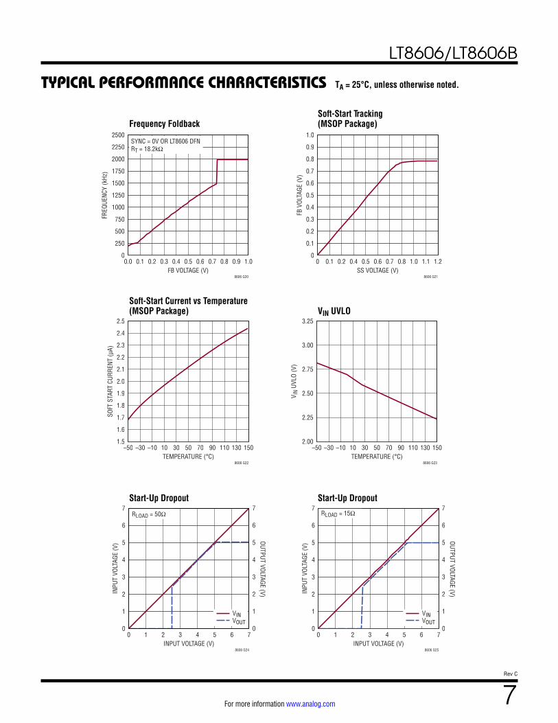
Frequency FoldbackSoft-Start Tracking (MSOP Package)
Soft-Start Current vs Temperature (MSOP Package) VIN UVLO
Start-Up Dropout Start-Up Dropout
FB VOLTAGE (V)0.0 0.1 0.2 0.3 0.4 0.5 0.6 0.7 0.8 0.9 1.0
0
250
500
750
1000
1250
1500
1750
2000
2250
2500
FREQ
UENC
Y (k
Hz)
8606 G20
SYNC = 0V OR LT8606 DFNRT = 18.2kΩ
SS VOLTAGE (V)0 0.1 0.2 0.4 0.5 0.6 0.7 0.8 1.0 1.1 1.2
0
0.1
0.2
0.3
0.4
0.5
0.6
0.7
0.8
0.9
1.0
FB V
OLTA
GE (V
)
8606 G21
TEMPERATURE (°C)–50 –30 –10 10 30 50 70 90 110 130 150
1.5
1.6
1.7
1.8
1.9
2.0
2.1
2.2
2.3
2.4
2.5
SOFT
STA
RT C
URRE
NT (µ
A)
8606 G22TEMPERATURE (°C)
–50 –30 –10 10 30 50 70 90 110 130 1502.00
2.25
2.50
2.75
3.00
3.25
V IN
UVLO
(V)
8606 G23
RLOAD = 50Ω
INPUT VOLTAGE (V)0 1 2 3 4 5 6 7
0
1
2
3
4
5
6
7
0
1
2
3
4
5
6
7
INPU
T VO
LTAG
E (V
)
OUTPUT VOLTAGE (V)
8606 G24
VINVOUT
RLOAD = 15Ω
INPUT VOLTAGE (V)0 1 2 3 4 5 6 7
0
1
2
3
4
5
6
7
0
1
2
3
4
5
6
7
INPU
T VO
LTAG
E (V
)
OUTPUT VOLTAGE (V)
8606 G25
VINVOUT
LT8606/LT8606B
8Rev C
For more information www.analog.com
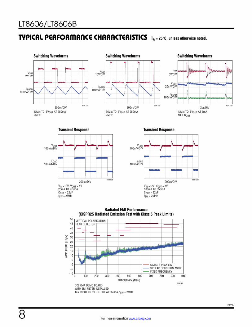
TYPICAL PERFORMANCE CHARACTERISTICS
Transient Response Transient Response
Switching Waveforms Switching Waveforms Switching Waveforms
200ns/DIV
VSW5V/DIV
ILOAD100mA/DIV
8606 G26
12VIN TO 5VOUT AT 250mA2MHz
200ns/DIV
VSW10V/DIV
ILOAD100mA/DIV
8606 G27
36VIN TO 5VOUT AT 250mA2MHz
2µs/DIV
SW5V/DIV
ILOAD100mA/DIV
VOUT20mV/DIV
8606 G28
12VIN TO 5VOUT AT 5mA10µF COUT
200µs/DIV
VOUT100mV/DIV
ILOAD100mA/DIV
8606 G29
VIN =12V, VOUT = 5V25mA TO 275mACOUT = 22µFfSW = 2MHz
200µs/DIV
VOUT100mV/DIV
ILOAD100mA/DIV
8606 G30
VIN =12V, VOUT = 5V100mA TO 350mACOUT = 22µFfSW = 2MHz
TA = 25°C, unless otherwise noted.
FREQUENCY (MHz)
AMPL
ITUD
E (d
BµV)
50
–5
40
25
15
5
30
45
35
20
10
0
–10
8606 G31
0 500 900300 700 1000400 800200 600100
VERTICAL POLARIZATIONPEAK DETECTOR
CLASS 5 PEAK LIMITSPREAD SPECTRUM MODEFIXED FREQUENCY
DC2564A DEMO BOARDWITH EMI FILTER INSTALLED14V INPUT TO 5V OUTPUT AT 350mA, fSW = 2MHz
Radiated EMI Performance (CISPR25 Radiated Emission Test with Class 5 Peak Limits)
LT8606/LT8606B
9Rev C
For more information www.analog.com
PIN FUNCTIONSBST: This pin is used to provide a drive voltage, higher than the input voltage, to the topside power switch. Place a 0.1µF boost capacitor as close as possible to the IC. Do not place a resistor in series with this pin.
SW: The SW pin is the output of the internal power switches. Connect this pin to the inductor and boost capacitor. This node should be kept small on the PCB for good performance.
INTVCC Internal 3.5V Regulator Bypass Pin. The internal power drivers and control circuits are powered from this voltage. INTVCC max output current is 20mA. Voltage on INTVCC will vary between 2.8V and 3.5V. Decouple this pin to power ground with at least a 1μF low ESR ceramic capacitor. Do not load the INTVCC pin with exter-nal circuitry.
RT: A resistor is tied between RT and ground to set the switching frequency. When synchronizing, the RT resistor should be chosen to set the LT8606 switching frequency to equal or below the lowest synchronization input.
SYNC (MSOP Only): External Clock Synchronization Input. Ground this pin for low ripple Burst Mode operation at low output loads. Tie to a clock source for synchroni-zation to an external frequency. Leave floating for pulse-skipping mode with no spread spectrum modulation. Tie to INTVCC or tie to a voltage between 3.2V and 5.0V for pulse-skipping mode with spread spectrum modulation. When in pulse-skipping mode, the IQ regulating no load will increase to several mA. There is no SYNC pin on the LT8606 DFN package. The LT8606 DFN package internally ties SYNC to ground. The LT8606B package internally floats SYNC.
FB: The LT8606 regulates the FB pin to 0.778V. Connect the feedback resistor divider tap to this pin.
TR/SS (MSOP Only): Output Tracking and Soft-Start Pin. This pin allows user control of output voltage ramp rate during start-up. A TR/SS voltage below 0.778V forces the LT8606 to regulate the FB pin to equal the TR/SS pin volt-age. When TR/SS is above 0.778V, the tracking function is disabled and the internal reference resumes control of the error amplifier. An internal 2μA pull-up current from INTVCC on this pin allows a capacitor to program out-put voltage slew rate. This pin is pulled to ground with a 300Ω MOSFET during shutdown and fault conditions; use a series resistor if driving from a low impedance output. There is no TR/SS pin on the LT8606 or LT8606B DFN and the node is internally floated.
PG: The PG pin is the open-drain output of an internal comparator. PG remains low until the FB pin is within ±8.5% of the final regulation voltage, and there are no fault conditions. PG is valid when VIN is above 3.2V and when EN/UV is high. PG is pulled low when VIN is above 3.2V and EN/UV is low. If VIN is near zero, PG will be high impedance.
VIN: The VIN pin supplies current to the LT8606 internal circuitry and to the internal topside power switch. This pin must be locally bypassed. Be sure to place the positive terminal of the input capacitor as close as possible to the VIN pins, and the negative capacitor terminal as close as possible to the GND pins.
EN/UV: The LT8606 is shut down when this pin is low and active when this pin is high. The hysteretic threshold volt-age is 1.05V going up and 1.00V going down. Tie to VIN if the shutdown feature is not used. An external resistor divider from VIN can be used to program a VIN threshold below which the LT8606 will shut down.
GND: Exposed Pad Pin. The exposed pad must be con-nected to the negative terminal of the input capacitor and soldered to the PCB in order to lower the thermal resistance.
LT8606/LT8606B
10Rev C
For more information www.analog.com
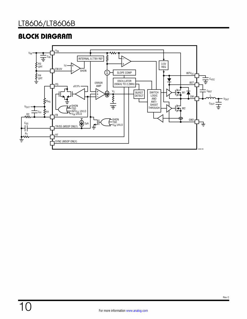
BLOCK DIAGRAM
++–
+–
SLOPE COMP
INTERNAL 0.778V REF
OSCILLATOR200kHz TO 2.2MHz
BURSTDETECT
3.5VREG
M1
M2
CBST
COUT
VOUT
8606 BD
SW L
BST
SWITCHLOGICANDANTI-
SHOOTTHROUGH
ERRORAMP
SHDN
±8.5%
VC
SHDNTSDINTVCC UVLOVIN UVLO
SHDNTSDVIN UVLO
EN/UV1V +
–INTVCC
GND
PG
FBR1
RPG
R2
RT
CSS
VOUT
CFF
TR/SS (MSOP ONLY)2µA
RT
SYNC (MSOP ONLY)
VINVIN
CIN
CVCC
R3OPT
R4OPT
LT8606/LT8606B
11Rev C
For more information www.analog.com
OPERATIONThe LT8606 is a monolithic constant frequency current mode step-down DC/DC converter. An oscillator with frequency set using a resistor on the RT pin turns on the internal top power switch at the beginning of each clock cycle. Current in the inductor then increases until the top switch current comparator trips and turns off the top power switch. The peak inductor current at which the top switch turns off is controlled by the voltage on the internal VC node. The error amplifier servos the VC node by comparing the voltage on the VFB pin with an inter-nal 0.778V reference. When the load current increases it causes a reduction in the feedback voltage relative to the reference leading the error amplifier to raise the VC volt-age until the average inductor current matches the new load current. When the top power switch turns off the synchronous power switch turns on until the next clock cycle begins or inductor current falls to zero. If overload conditions result in excess current flowing through the bottom switch, the next clock cycle will be delayed until switch current returns to a safe level.
If the EN/UV pin is low, the LT8606 is shut down and draws 1µA from the input. When the EN/UV pin is above 1.05V, the switching regulator becomes active.
To optimize efficiency at light loads, the LT8606 enters Burst Mode operation during light load situations.
Between bursts, all circuitry associated with controlling the output switch is shut down, reducing the input supply current to 1.7μA. In a typical application, 3.0μA will be consumed from the input supply when regulating with no load. The SYNC pin is tied low to use Burst Mode opera-tion and can be floated to use pulse-skipping mode. If a clock is applied to the SYNC pin the part will synchronize to an external clock frequency and operate in pulse-skip-ping mode. While in pulse-skipping mode the oscillator operates continuously and positive SW transitions are aligned to the clock. During light loads, switch pulses are skipped to regulate the output and the quiescent cur-rent will be several mA. The SYNC pin may be tied high for spread spectrum modulation mode, and the LT8606 will operate similar to pulse-skipping mode but vary the clock frequency to reduce EMI. The LT8606 DFN has no SYNC pin and will always operate in Burst Mode opera-tion. The LT8606B has no SYNC pin and will operate in pulse-skipping mode.
Comparators monitoring the FB pin voltage will pull the PG pin low if the output voltage varies more than ±8.5% (typi-cal) from the set point, or if a fault condition is present.
The oscillator reduces the LT8606’s operating frequency when the voltage at the FB pin is low and the part is in Burst Mode operation. This frequency foldback helps to control the inductor current when the output voltage is lower than the programmed value which occurs during start-up.
LT8606/LT8606B
12Rev C
For more information www.analog.com
APPLICATIONS INFORMATION
Achieving Ultralow Quiescent Current
To enhance efficiency at light loads, the LT8606 enters into low ripple Burst Mode operation, which keeps the output capacitor charged to the desired output voltage while minimizing the input quiescent current and mini-mizing output voltage ripple. In Burst Mode operation the LT8606 delivers single small pulses of current to the out-put capacitor followed by sleep periods where the output power is supplied by the output capacitor. While in sleep mode the LT8606 consumes 1.7μA.
As the output load decreases, the frequency of single cur-rent pulses decreases (see Figure 1) and the percentage of time the LT8606 is in sleep mode increases, result-ing in much higher light load efficiency than for typical converters. By maximizing the time between pulses, the converter quiescent current approaches 3.0µA for a typi-cal application when there is no output load. Therefore, to optimize the quiescent current performance at light loads, the current in the feedback resistor divider must be minimized as it appears to the output as load current.
While in Burst Mode operation the current limit of the top switch is approximately 150mA resulting in output voltage ripple shown in Figure 3. Increasing the output capacitance will decrease the output ripple proportionally. As load ramps upward from zero the switching frequency will increase but only up to the switching frequency pro-grammed by the resistor at the RT pin as shown in Table 1. The output load at which the LT8606 reaches the pro-grammed frequency varies based on input voltage, output voltage, and inductor choice.
For some applications it is desirable for the LT8606 to operate in pulse-skipping mode, offering two major differ-ences from Burst Mode operation. First is the clock stays awake at all times and all switching cycles are aligned to the clock. In this mode much of the internal circuitry is awake at all times, increasing quiescent current to several hundred µA. Second is that full switching frequency is reached at lower output load than in Burst Mode operation as shown in Figure 2. To enable pulse-skipping mode the SYNC pin is floated. To achieve spread spectrum modula-tion with pulse-skipping mode, the SYNC pin is tied high. While a clock is applied to the SYNC pin the LT8606 will
Figure 2. Full Switching Frequency Minimum Load vs VIN in Pulse Skipping Mode (MSOP ONLY)
Figure 3. Burst Mode Operation
Figure 1. SW Burst Mode Frequency vs Output Current
0 25 50 75 100 1250
250
500
750
1000
1250
1500
1750
2000
2250
2500
SWIT
CHIN
G FR
EQUE
NCY
(kHz
)
8606 F01
L = 6.8µHVIN = 12VVOUT = 3.3VSYNC = 0V
OUTPUT CURRENT (mA)
INPUT VOLTAGE (V)0 5 10 15 20 25 30 35 40 45
0
5
10
15
20
OUTP
UT C
URRE
NT (m
A)
8606 F02
L = 10µHVIN = 12VVOUT = 5VRT = 18.2kΩ
2µs/DIV
SW5V/DIV
ILOAD100mA/DIV
VOUT20mV/DIV
8606 F03
also operate in pulse-skipping mode. The LT8606 DFN is always programmed for Burst Mode operation and cannot enter pulse-skipping mode. The LT8606B DFN is programmed for pulse-skipping mode and cannot enter Burst Mode operation.
LT8606/LT8606B
13Rev C
For more information www.analog.com
APPLICATIONS INFORMATIONFB Resistor Network
The output voltage is programmed with a resistor divider between the output and the FB pin. Choose the resistor values according to:
R1=R2 VOUT
0.778V–1⎛
⎝⎜⎞⎠⎟
1% resistors are recommended to maintain output volt-age accuracy.
The total resistance of the FB resistor divider should be selected to be as large as possible when good low load efficiency is desired: The resistor divider generates a small load on the output, which should be minimized to optimize the quiescent current at low loads.
When using large FB resistors, a 10pF phase lead capaci-tor should be connected from VOUT to FB.
Setting the Switching Frequency
The LT8606 uses a constant frequency PWM architec-ture that can be programmed to switch from 200kHz to 2.2MHz by using a resistor tied from the RT pin to ground. A table showing the necessary RT value for a desired switching frequency is in Table 1. When in spread spectrum modulation mode, the frequency is modulated upwards of the frequency set by RT.
Table 1. SW Frequency vs RT ValuefSW (MHz) RT (kΩ)
0.2 2210.300 1430.400 1100.500 86.60.600 71.50.700 60.40.800 52.30.900 46.41.000 40.21.200 33.21.400 27.41.600 23.71.800 20.52.000 18.22.200 16.2
Operating Frequency Selection and Trade-Offs
Selection of the operating frequency is a trade-off between efficiency, component size, and input voltage range. The advantage of high frequency operation is that smaller inductor and capacitor values may be used. The disad-vantages are lower efficiency and a smaller input voltage range.
The highest switching frequency (fSW(MAX)) for a given application can be calculated as follows:
fSW(MAX) =VOUT + VSW(BOT)
tON(MIN) VIN – VSW(TOP) + VSW(BOT)( )where VIN is the typical input voltage, VOUT is the output voltage, VSW(TOP) and VSW(BOT) are the internal switch drops (~0.13V, ~0.06V, respectively at max load) and tON(MIN) is the minimum top switch on-time (see Electrical Characteristics). This equation shows that slower switch-ing frequency is necessary to accommodate a high VIN/VOUT ratio.
For transient operation VIN may go as high as the Abs Max rating regardless of the RT value, however the LT8606 will reduce switching frequency as necessary to maintain control of inductor current to assure safe operation.
The LT8606 is capable of maximum duty cycle approach-ing 100%, and the VIN to VOUT dropout is limited by the RDS(ON) of the top switch. In this mode the LT8606 skips switch cycles, resulting in a lower switching frequency than programmed by RT.
For applications that cannot allow deviation from the pro-grammed switching frequency at low VIN/VOUT ratios use the following formula to set switching frequency:
VIN(MIN) =
VOUT + VSW(BOT)
1– fSW • tOFF(MIN)– VSW(BOT) + VSW(TOP)
where VIN(MIN) is the minimum input voltage without skipped cycles, VOUT is the output voltage, VSW(TOP) and VSW(BOT) are the internal switch drops (~0.13V, ~0.06V, respectively at max load), fSW is the switching frequency (set by RT), and tOFF(MIN) is the minimum switch off-time. Note that higher switching frequency will increase the minimum input voltage below which cycles will be dropped to achieve higher duty cycle.
LT8606/LT8606B
14Rev C
For more information www.analog.com
APPLICATIONS INFORMATIONInductor Selection and Maximum Output Current
The LT8606 is designed to minimize solution size by allowing the inductor to be chosen based on the output load requirements of the application. During overload or short circuit conditions the LT8606 safely tolerates opera-tion with a saturated inductor through the use of a high speed peak-current mode architecture.
A good first choice for the inductor value is:
L =
VOUT + VSW(BOT)
fSW• 4
where fSW is the switching frequency in MHz, VOUT is the output voltage, VSW(BOT) is the bottom switch drop (~0.06V) and L is the inductor value in μH.
To avoid overheating and poor efficiency, an inductor must be chosen with an RMS current rating that is greater than the maximum expected output load of the applica-tion. In addition, the saturation current (typically labeled ISAT) rating of the inductor must be higher than the load current plus 1/2 of in inductor ripple current:
IL(PEAK) = ILOAD(MAX)+
12ΔL
where ∆IL is the inductor ripple current as calculated sev-eral paragraphs below and ILOAD(MAX) is the maximum output load for a given application.
As a quick example, an application requiring 0.25A output should use an inductor with an RMS rating of greater than 0.5A and an ISAT of greater than 0.7A. To keep the efficiency high, the series resistance (DCR) should be less than 0.04Ω, and the core material should be intended for high frequency applications.
The LT8606 limits the peak switch current in order to protect the switches and the system from overload faults. The top switch current limit (ILIM) is at least 0.65A at low duty cycles and decreases linearly to at least 0.5A at D = 0.8. The inductor value must then be sufficient to supply the desired maximum output current (IOUT(MAX)), which is a function of the switch current limit (ILIM) and the ripple current:
IOUT(MAX) = ILIM –
ΔIL2
The peak-to-peak ripple current in the inductor can be calculated as follows:
ΔIL =
VOUTL • fSW
1–VOUT
VIN(MAX)
⎛
⎝⎜
⎞
⎠⎟
where fSW is the switching frequency of the LT8606, and L is the value of the inductor. Therefore, the maximum output current that the LT8606 will deliver depends on the switch current limit, the inductor value, and the input and output voltages. The inductor value may have to be increased if the inductor ripple current does not allow sufficient maximum output current (IOUT(MAX)) given the switching frequency, and maximum input voltage used in the desired application.
The optimum inductor for a given application may differ from the one indicated by this design guide. A larger value inductor provides a higher maximum load current and reduces the output voltage ripple. For applications requir-ing smaller load currents, the value of the inductor may be lower and the LT8606 may operate with higher ripple current. This allows use of a physically smaller inductor, or one with a lower DCR resulting in higher efficiency. Be aware that low inductance may result in discontinuous mode operation, which further reduces maximum load current.
For more information about maximum output current and discontinuous operation, see Analog Devices Application Note 44.
Finally, for duty cycles greater than 50% (VOUT/VIN > 0.5), a minimum inductance is required to avoid sub-harmonic oscillation. See Application Note 19.
Input Capacitor
Bypass the input of the LT8606 circuit with a ceramic capacitor of X7R or X5R type. Y5V types have poor per-formance over temperature and applied voltage, and should not be used. A 4.7μF to 10μF ceramic capacitor is adequate to bypass the LT8606 and will easily handle the ripple current. Note that larger input capacitance is required when a lower switching frequency is used. If the input power source has high impedance, or there is
LT8606/LT8606B
15Rev C
For more information www.analog.com
APPLICATIONS INFORMATIONsignificant inductance due to long wires or cables, addi-tional bulk capacitance may be necessary. This can be provided with a low performance electrolytic capacitor.
Step-down regulators draw current from the input sup-ply in pulses with very fast rise and fall times. The input capacitor is required to reduce the resulting voltage rip-ple at the LT8606 and to force this very high frequency switching current into a tight local loop, minimizing EMI. A 4.7μF capacitor is capable of this task, but only if it is placed close to the LT8606 (see the PCB Layout section). A second precaution regarding the ceramic input capaci-tor concerns the maximum input voltage rating of the LT8606. A ceramic input capacitor combined with trace or cable inductance forms a high quality (under damped) tank circuit. If the LT8606 circuit is plugged into a live supply, the input voltage can ring to twice its nominal value, possibly exceeding the LT8606’s voltage rating. This situation is easily avoided (see Analog Devices Application Note 88).
Output Capacitor and Output Ripple
The output capacitor has two essential functions. Along with the inductor, it filters the square wave generated by the LT8606 to produce the DC output. In this role it determines the output ripple, thus low impedance at the switching frequency is important. The second function is to store energy in order to satisfy transient loads and sta-bilize the LT8606’s control loop. Ceramic capacitors have very low equivalent series resistance (ESR) and provide the best ripple performance. A good starting value is:
COUT =
100VOUT • fSW
where fSW is in MHz, and COUT is the recommended output capacitance in μF. Use X5R or X7R types. This choice will provide low output ripple and good tran-sient response. Transient performance can be improved with a higher value output capacitor and the addition of a feedforward capacitor placed between VOUT and FB. Increasing the output capacitance will also decrease the output voltage ripple. A lower value of output capacitor
can be used to save space and cost but transient per-formance will suffer and may cause loop instability. See the Typical Applications in this data sheet for suggested capacitor values.
When choosing a capacitor, special attention should be given to the data sheet to calculate the effective capaci-tance under the relevant operating conditions of voltage bias and temperature. A physically larger capacitor or one with a higher voltage rating may be required.
Ceramic Capacitors
Ceramic capacitors are small, robust and have very low ESR. However, ceramic capacitors can cause problems when used with the LT8606 due to their piezoelectric nature. When in Burst Mode operation, the LT8606’s switching frequency depends on the load current, and at very light loads the LT8606 can excite the ceramic capacitor at audio frequencies, generating audible noise. Since the LT8606 operates at a lower current limit during Burst Mode operation, the noise is typically very quiet to a casual ear. If this is unacceptable, use a high performance tantalum or electrolytic capacitor at the output.
A final precaution regarding ceramic capacitors concerns the maximum input voltage rating of the LT8606. As pre-viously mentioned, a ceramic input capacitor combined with trace or cable inductance forms a high quality (under damped) tank circuit. If the LT8606 circuit is plugged into a live supply, the input voltage can ring to twice its nomi-nal value, possibly exceeding the LT8606’s rating. This situation is easily avoided (see Analog Devices Application Note 88).
Enable Pin
The LT8606 is in shutdown when the EN pin is low and active when the pin is high. The rising threshold of the EN comparator is 1.05V, with 50mV of hysteresis. The EN pin can be tied to VIN if the shutdown feature is not used, or tied to a logic level if shutdown control is required.
Adding a resistor divider from VIN to EN programs the LT8606 to regulate the output only when VIN is above a desired voltage (see Block Diagram). Typically, this threshold, VIN(EN), is used in situations where the input
LT8606/LT8606B
16Rev C
For more information www.analog.com
supply is current limited, or has a relatively high source resistance. A switching regulator draws constant power from the source, so source current increases as source voltage drops. This looks like a negative resistance load to the source and can cause the source to current limit or latch low under low source voltage conditions. The VIN(EN) threshold prevents the regulator from operating at source voltages where the problems might occur. This threshold can be adjusted by setting the values R3 and R4 such that they satisfy the following equation:
VIN(EN) =
R3R4
+1⎛⎝⎜
⎞⎠⎟ •1V
where the LT8606 will remain off until VIN is above VIN(EN). Due to the comparator’s hysteresis, switching will not stop until the input falls slightly below VIN(EN).
When in Burst Mode operation for light-load currents, the current through the VIN(EN) resistor network can eas-ily be greater than the supply current consumed by the LT8606. Therefore, the VIN(EN) resistors should be large to minimize their effect on efficiency at low loads.
INTVCC Regulator
An internal low dropout (LDO) regulator produces the 3.5V supply from VIN that powers the drivers and the internal bias circuitry. The INTVCC can supply enough cur-rent for the LT8606’s circuitry and must be bypassed to ground with a minimum of 1μF ceramic capacitor. Good bypassing is necessary to supply the high transient currents required by the power MOSFET gate drivers. Applications with high input voltage and high switching frequency will increase die temperature because of the higher power dissipation across the LDO. Do not connect an external load to the INTVCC pin.
Output Voltage Tracking and Soft-Start (MSOP ONLY)
The LT8606 allows the user to program its output voltage ramp rate by means of the TR/SS pin. An internal 2μA pulls up the TR/SS pin to INTVCC. Putting an external capacitor on TR/SS enables soft-starting the output to prevent current surge on the input supply. During the soft-start ramp the output voltage will proportionally track the
APPLICATIONS INFORMATIONTR/SS pin voltage. For output tracking applications, TR/SS can be externally driven by another voltage source. From 0V to 0.778V, the TR/SS voltage will override the internal 0.778V reference input to the error amplifier, thus regulating the FB pin voltage to that of TR/SS pin. When TR/SS is above 0.778V, tracking is disabled and the feed-back voltage will regulate to the internal reference voltage.
An active pull-down circuit is connected to the TR/SS pin which will discharge the external soft-start capacitor in the case of fault conditions and restart the ramp when the faults are cleared. Fault conditions that clear the soft-start capacitor are the EN/UV pin transitioning low, VIN voltage falling too low, or thermal shutdown. The LT8606 and LT8606B DFN does not have TR/SS pin or functionality.
Output Power Good
When the LT8606’s output voltage is within the ±8.5% window of the regulation point, which is a VFB voltage in the range of 0.716V to 0.849V (typical), the output voltage is considered good and the open-drain PG pin goes high impedance and is typically pulled high with an external resistor. Otherwise, the internal drain pull-down device will pull the PG pin low. To prevent glitching both the upper and lower thresholds include 0.5% of hysteresis.
The PG pin is also actively pulled low during several fault conditions: EN/UV pin is below 1V, INTVCC has fallen too low, VIN is too low, or thermal shutdown.
Synchronization (MSOP ONLY)
To select low ripple Burst Mode operation, tie the SYNC pin below 0.4V (this can be ground or a logic low out-put). To synchronize the LT8606 oscillator to an external frequency connect a square wave (with 20% to 80% duty cycle) to the SYNC pin. The square wave amplitude should have valleys that are below 0.9V and peaks above 2.7V (up to 5V).
The LT8606 will not enter Burst Mode operation at low output loads while synchronized to an external clock, but instead will pulse skip to maintain regulation. The LT8606 may be synchronized over a 200kHz to 2.2MHz range. The RT resistor should be chosen to set the LT8606 switching
LT8606/LT8606B
17Rev C
For more information www.analog.com
APPLICATIONS INFORMATIONfrequency equal to or below the lowest synchronization input. For example, if the synchronization signal will be 500kHz and higher, the RT should be selected for 500kHz. The slope compensation is set by the RT value, while the minimum slope compensation required to avoid subhar-monic oscillations is established by the inductor size, input voltage, and output voltage. Since the synchroniza-tion frequency will not change the slopes of the inductor current waveform, if the inductor is large enough to avoid subharmonic oscillations at the frequency set by RT, then the slope compensation will be sufficient for all synchro-nization frequencies.
For some applications it is desirable for the LT8606 to operate in pulse-skipping mode, offering two major differ-ences from Burst Mode operation. First is the clock stays awake at all times and all switching cycles are aligned to the clock. Second is that full switching frequency is reached at lower output load than in Burst Mode opera-tion as shown in Figure 2 in an earlier section. These two differences come at the expense of increased quiescent current. To enable pulse-skipping mode the SYNC pin is floated.
For some applications, reduced EMI operation may be desirable, which can be achieved through spread spec-trum modulation. This mode operates similar to pulse skipping mode operation, with the key difference that the switching frequency is modulated up and down by a 3kHz triangle wave. The modulation has the frequency set by RT as the low frequency, and modulates up to approximately 20% higher than the frequency set by RT. To enable spread spectrum mode, tie SYNC to INTVCC or drive to a voltage between 3.2V and 5V.
The LT8606 does not operate in forced continuous mode regardless of SYNC signal. The LT8606 DFN is always programmed for Burst Mode operation and cannot enter pulse-skipping mode. The LT8606B DFN is programmed for pulse-skipping mode and cannot enter Burst Mode operation.
Shorted and Reversed Input Protection
The LT8606 will tolerate a shorted output. Several features are used for protection during output short-circuit and brownout conditions. The first is the switching frequency
will be folded back while the output is lower than the set point to maintain inductor current control. Second, the bottom switch current is monitored such that if inductor current is beyond safe levels switching of the top switch will be delayed until such time as the inductor current falls to safe levels. This allows for tailoring the LT8606 to individual applications and limiting thermal dissipation during short circuit conditions.
Frequency foldback behavior depends on the state of the SYNC pin: If the SYNC pin is low, the switching frequency will slow while the output voltage is lower than the pro-grammed level. If the SYNC pin is connected to a clock source, tied high or floated, the LT8606 will stay at the programmed frequency without foldback and only slow switching if the inductor current exceeds safe levels.
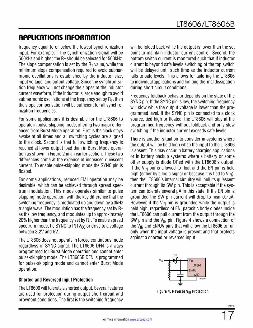
There is another situation to consider in systems where the output will be held high when the input to the LT8606 is absent. This may occur in battery charging applications or in battery backup systems where a battery or some other supply is diode ORed with the LT8606’s output. If the VIN pin is allowed to float and the EN pin is held high (either by a logic signal or because it is tied to VIN), then the LT8606’s internal circuitry will pull its quiescent current through its SW pin. This is acceptable if the sys-tem can tolerate several μA in this state. If the EN pin is grounded the SW pin current will drop to near 0.7µA. However, if the VIN pin is grounded while the output is held high, regardless of EN, parasitic body diodes inside the LT8606 can pull current from the output through the SW pin and the VIN pin. Figure 4 shows a connection of the VIN and EN/UV pins that will allow the LT8606 to run only when the input voltage is present and that protects against a shorted or reversed input.
VINVIN
LT8606
GND
D1
8606 F04
EN/UV
Figure 4. Reverse VIN Protection
LT8606/LT8606B
18Rev C
For more information www.analog.com
APPLICATIONS INFORMATIONthe ground plane as much as possible, and add thermal vias under and near the LT8606 to additional ground planes within the circuit board and on the bottom side.
Thermal Considerations
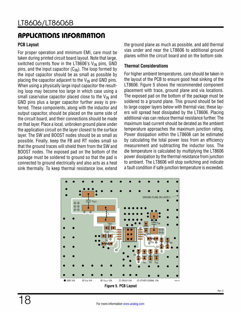
For higher ambient temperatures, care should be taken in the layout of the PCB to ensure good heat sinking of the LT8606. Figure 5 shows the recommended component placement with trace, ground plane and via locations. The exposed pad on the bottom of the package must be soldered to a ground plane. This ground should be tied to large copper layers below with thermal vias; these lay-ers will spread heat dissipated by the LT8606. Placing additional vias can reduce thermal resistance further. The maximum load current should be derated as the ambient temperature approaches the maximum junction rating. Power dissipation within the LT8606 can be estimated by calculating the total power loss from an efficiency measurement and subtracting the inductor loss. The die temperature is calculated by multiplying the LT8606 power dissipation by the thermal resistance from junction to ambient. The LT8606 will stop switching and indicate a fault condition if safe junction temperature is exceeded.
PCB Layout
For proper operation and minimum EMI, care must be taken during printed circuit board layout. Note that large, switched currents flow in the LT8606’s VIN pins, GND pins, and the input capacitor (CIN). The loop formed by the input capacitor should be as small as possible by placing the capacitor adjacent to the VIN and GND pins. When using a physically large input capacitor the result-ing loop may become too large in which case using a small case/value capacitor placed close to the VIN and GND pins plus a larger capacitor further away is pre-ferred. These components, along with the inductor and output capacitor, should be placed on the same side of the circuit board, and their connections should be made on that layer. Place a local, unbroken ground plane under the application circuit on the layer closest to the surface layer. The SW and BOOST nodes should be as small as possible. Finally, keep the FB and RT nodes small so that the ground traces will shield them from the SW and BOOST nodes. The exposed pad on the bottom of the package must be soldered to ground so that the pad is connected to ground electrically and also acts as a heat sink thermally. To keep thermal resistance low, extend
Figure 5. PCB Layout
8606 F05GND VIA VIN VIA VOUT VIA EN/UV VIA OTHER SIGNAL VIA
COUT
CINCBST
CVCC
GROUND PLANE ON LAYER 2
RT
L
CIN(OPT)
R1
CFF R2
R4
R3
RPG
1
CSS
LT8606/LT8606B
19Rev C
For more information www.analog.com
TYPICAL APPLICATIONS
VIN BSTEN/UV
C10.1µF
C510pF
R21M
VIN5.5V TO 42V
C610nF
C31µF
VOUT5V350mA
POWER GOOD
R3187k
8606 TA02
L110µH
SYNC
INTVCC
TR/SS
RT
LT8606
GND
SW
PG
FB
R4100k
R118.2k
L1 = XFL3010-103ME
C410µFX7R0805
fSW = 2MHz
C21µFX7R0805
VIN BSTEN/UV
C10.1µF
C510pF
R21M
VIN3.8V TO 42V
C610nF
C31µF
VOUT3.3V350mA
POWER GOOD
R3309k
8606 TA03
L16.8µH
SYNC
INTVCC
TR/SS
RT
LT8606
GND
SW
PG
FB
R4100k
R118.2k
L1 = XFL3010-682ME
C410µFX7R0805
fSW = 2MHz
C21µFX7R0805
VIN BSTEN/UV
C10.1µF
C5100pF
R21M
VIN12.7V TO 42V
C610nF
C31µF
VOUT12V350mA
POWER GOOD
R369.8k
8606 TA04
L147µH
SYNC
INTVCC
TR/SS
RT
LT8606
GND
SW
PG
FB
R4100k
R140.2k
L1 = MSS6132-473MLB
C422µFX7R1210
fSW = 1MHz
C24.7µFX7R1206
5V 2MHz Step Down
3.3V 2MHz Step Down
12V 1MHz Step Down
LT8606/LT8606B
20Rev C
For more information www.analog.com
VIN BSTEN/UV
C10.1µF
C510pF
R21M
VIN3.2V TO 20V
(42V TRANSIENT)
C610nF
C31µF
VOUT1.8V350mA
POWER GOOD
R3768k
8606 TA05
L13.3µH
SYNC
INTVCC
TR/SS
RT
LT8606
GND
SW
PG
FB
R4100k
R118.2k
L1 = XFL3010-332ME
C422µFX7R1206
fSW = 2MHz
C24.7µF
VIN BSTEN/UV
C10.1µF
C547pF
R21M
VIN5.8 TO 40V
C610nF
C31µF
VOUT5V350mA
POWER GOOD
R3187k
8606 TA06
L127µH
L34.7µH
L2BEAD
SYNC
INTVCC
TR/SS
RT
LT8606(MSOP)
GND
SW
PG
FB
R4100k
R160.4k
C422µFX7R1206
fSW = 700kHz
C24.7µF
C933µF
C74.7µF
C84.7µF
C8, C7, C2: X7R 1206C9: 63SXV33ML1: MSS5121-273L2: MPZ2012S221AT000L3: XAL4030-472
Ultralow EMI 5V 1.5A Step Down
1.8V 2MHz Step Down
TYPICAL APPLICATIONS
LT8606/LT8606B
21Rev C
For more information www.analog.com
PACKAGE DESCRIPTION
MSOP (MSE) 0213 REV I
0.53 ±0.152(.021 ±.006)
SEATINGPLANE
0.18(.007)
1.10(.043)MAX
0.17 – 0.27(.007 – .011)
TYP
0.86(.034)REF
0.50(.0197)
BSC
1 2 3 4 5
4.90 ±0.152(.193 ±.006)
0.497 ±0.076(.0196 ±.003)
REF8910
10
1
7 6
3.00 ±0.102(.118 ±.004)
(NOTE 3)
3.00 ±0.102(.118 ±.004)
(NOTE 4)
NOTE:1. DIMENSIONS IN MILLIMETER/(INCH)2. DRAWING NOT TO SCALE3. DIMENSION DOES NOT INCLUDE MOLD FLASH, PROTRUSIONS OR GATE BURRS. MOLD FLASH, PROTRUSIONS OR GATE BURRS SHALL NOT EXCEED 0.152mm (.006") PER SIDE4. DIMENSION DOES NOT INCLUDE INTERLEAD FLASH OR PROTRUSIONS. INTERLEAD FLASH OR PROTRUSIONS SHALL NOT EXCEED 0.152mm (.006") PER SIDE5. LEAD COPLANARITY (BOTTOM OF LEADS AFTER FORMING) SHALL BE 0.102mm (.004") MAX6. EXPOSED PAD DIMENSION DOES INCLUDE MOLD FLASH. MOLD FLASH ON E-PAD SHALL NOT EXCEED 0.254mm (.010") PER SIDE.
0.254(.010) 0° – 6° TYP
DETAIL “A”
DETAIL “A”
GAUGE PLANE
5.10(.201)MIN
3.20 – 3.45(.126 – .136)
0.889 ±0.127(.035 ±.005)
RECOMMENDED SOLDER PAD LAYOUT
1.68 ±0.102(.066 ±.004)
1.88 ±0.102(.074 ±.004)
0.50(.0197)
BSC0.305 ± 0.038(.0120 ±.0015)
TYP
BOTTOM VIEW OFEXPOSED PAD OPTION
1.68(.066)
1.88(.074)
0.1016 ±0.0508(.004 ±.002)
DETAIL “B”
DETAIL “B”CORNER TAIL IS PART OF
THE LEADFRAME FEATURE.FOR REFERENCE ONLY
NO MEASUREMENT PURPOSE
0.05 REF
0.29REF
MSE Package10-Lead Plastic MSOP, Exposed Die Pad
(Reference LTC DWG # 05-08-1664 Rev I)
LT8606/LT8606B
22Rev C
For more information www.analog.com
PACKAGE DESCRIPTION
2.00 ±0.05(4 SIDES)
2.00 SQ ±0.05
NOTE:1. DRAWING IS NOT A JEDEC PACKAGE OUTLINE2. DRAWING NOT TO SCALE3. ALL DIMENSIONS ARE IN MILLIMETERS4. DIMENSIONS OF EXPOSED PAD ON BOTTOM OF PACKAGE DO NOT INCLUDE MOLD FLASH. MOLD FLASH, IF PRESENT, SHALL NOT EXCEED 0.15mm ON ANY SIDE5. EXPOSED PAD SHALL BE SOLDER PLATED 6. SHADED AREA IS ONLY A REFERENCE FOR PIN 1 LOCATION ON THE TOP AND BOTTOM OF PACKAGE
0.55 ±0.05
BOTTOM VIEW—EXPOSED PAD
0.23REF0.335
REF
0.335 REF
0.75 ±0.05
14
85
PIN 1 BARTOP MARK
(SEE NOTE 6)
0.200 REF
0.00 – 0.05
(DC8MA) DFN 0113 REV Ø
0.23 ±0.050.45 BSC
0.25 ±0.05
RECOMMENDED SOLDER PAD PITCH AND DIMENSIONSAPPLY SOLDER MASK TO AREAS THAT ARE NOT SOLDERED
0.90REF
0.23REF
0.85 ±0.05
1.8 REF
1.8 REF
2.60 ±0.05
PACKAGEOUTLINE
0.45 BSC
PIN 1 NOTCH R = 0.15
DC8 Package8-Lead Plastic DFN (2mm × 2mm)
(Reference LTC DWG # 05-08-1939 Rev Ø)Exposed Pad Variation AA
LT8606/LT8606B
23Rev C
For more information www.analog.com
Information furnished by Analog Devices is believed to be accurate and reliable. However, no responsibility is assumed by Analog Devices for its use, nor for any infringements of patents or other rights of third parties that may result from its use. Specifications subject to change without notice. No license is granted by implication or otherwise under any patent or patent rights of Analog Devices.
REVISION HISTORYREV DATE DESCRIPTION PAGE NUMBER
A 06/17 Added DFN package optionClarified electrical parameters for DFN package optionClarified graphs for MSOP package optionClarified Pin Functions for DFN package optionClarified Operation section to include DFN option Clarified Applications last paragraph and Figure 2 to include DFN option Clarified Applications section to include DFN operation Added DFN Package Description
1,22,36,79
1112
16,1722
B 11/17 Added H-grade option Clarified Oscillator Frequency RT conditionsClarified efficiency graphsClarified Frequency Foldback graphClarified Switching Waveform graphClarified Block DiagramAdded Figure 5Clarified Typical Applications for MSOP package option
2, 33478
1018
20, 24
C 07/18 Added B version Added table to clarify versionsModified text in Description to add DFN functionalityAdded B version to Order InformationClarified Minimum On-Time ConditionsClarified Efficiency graphsClarified No-Load Supply Current graphsClarified Burst Frequency vs Output Current graphClarified Frequency Foldback graphClarified Pin Functions on SYNC and TR/SSClarified Operation third paragraphClarified last paragraph to include DFN B versionClarified Applications Information to include DFN B versionClarified Figure 5 PCB Layout
All112345679
1112
16, 1718
LT8606/LT8606B
24Rev C
For more information www.analog.com ANALOG DEVICES, INC. 2017-2018
D17104-0-7/18(C)www.analog.com
RELATED PARTS
TYPICAL APPLICATION
PART NUMBER DESCRIPTION COMMENTSLT8607 42V, 750mA, 92% Efficiency, 2.2MHz Synchronous MicroPower
Step-Down DC/DC Converter with IQ = 3µA VIN = 3V to 42V, VOUT(MIN) = 0.778V, IQ = 3µA, ISD < 1µA, MSOP-10E Package
LT8608 42V, 1.5A, 92% Efficiency, 2.2MHz Synchronous MicroPower Step-Down DC/DC Converter with IQ = 2.5µA
VIN = 3V to 42V, VOUT(MIN) = 0.778V, IQ = 2.5µA, ISD < 1µA, MSOP-10E Package
LT8609/LT8609A/LT8609B
42V, 2A/3A Peak, 93% Efficiency, 2.2MHz Synchronous MicroPower Step-Down DC/DC Converter with IQ = 2.5µA
VIN = 3V to 42V, VOUT(MIN) = 0.782V, IQ = 2.5µA, ISD < 1µA, MSOP-10E Package
LT8609S 42V, 2A/3A Peak, 93% Efficiency, 2.2MHz Synchronous Silent Switcher 2 Step-Down DC/DC Converter with IQ = 2.5µA
VIN = 3V to 42V, VOUT(MIN) = 0.774V, IQ = 2.5µA, ISD < 1µA, 3mm × 3mm LQFN-16 Package
LT8610A/ LT8610AB/LT8610AC
42V, 3.5A, 96% Efficiency, 2.2MHz Synchronous MicroPower Step-Down DC/DC Converter with IQ = 2.5µA
VIN = 3.4V to 42V, VOUT(MIN) = 0.97V, IQ = 2.5µA, ISD < 1µA, MSOP-16E Package
LT8616 42V, Dual 2.5A + 1.5A, 95% Efficiency, 2.2MHz Synchronous MicroPower Step-Down DC/DC Converter with IQ = 5µA
VIN = 3.4V to 42V, VOUT(MIN) = 0.8V, IQ = 5µA, ISD < 1µA, TSSOP-28E, 3mm × 6mm QFN-28 Packages
LT8620 65V, 2.5A, 96% Efficiency, 2.2MHz Synchronous MicroPower Step-Down DC/DC Converter with IQ = 2.5µA
VIN = 3.4V to 65V, VOUT(MIN) = 0.97V, IQ = 2.5µA, ISD < 1µA, MSOP-16E, 3mm × 5mm QFN-24 Packages
LT8614 42V, 4A, 96% Efficiency, 2.2MHz Synchronous MicroPower Step-Down DC/DC Converter with IQ = 2.5µA
VIN = 3.4V to 42V, VOUT(MIN) = 0.97V, IQ = 2.5µA, ISD < 1µA, 3mm × 4mm QFN-18 Package
LT8612 42V, 6A, 96% Efficiency, 2.2MHz Synchronous MicroPower Step-Down DC/DC Converter with IQ = 2.5µA
VIN = 3.4V to 42V, VOUT(MIN) = 0.97V, IQ = 3.0µA, ISD < 1µA, 3mm × 6mm QFN-28 Package
LT8640 42V, 5A, 96% Efficiency, 3MHz Synchronous MicroPower Step-Down DC/DC Converter with IQ = 2.5µA
VIN = 3.4V to 42V, VOUT(MIN) = 0.97V, IQ = 2.5µA, ISD < 1µA, 3mm × 4mm QFN-18 Package
LT8640S 42V, 6A, 96% Efficiency, 3MHz Synchronous Silent Switcher 2 Step-Down DC/DC Converter with IQ = 2.5µA
VIN = 3.4V to 42V, VOUT(MIN) = 0.97V, IQ = 2.5µA, ISD < 1µA, 4mm × 4mm LQFN-24 Package
LT8645S 65V, 8A, 96% Efficiency, 3MHz Synchronous Silent Switcher 2 Step-Down DC/DC Converter with IQ = 2.5µA
VIN = 3.4V to 65V, VOUT(MIN) = 0.97V, IQ = 2.5µA, ISD < 1µA, 4mm × 6mm LQFN-32 Package
LT8602 42V, Quad Output (2.5A+1.5A+1.5A+1.5A) 95% Efficiency, 2.2MHz Synchronous MicroPower Step-Down DC/DC Converter with IQ = 25µA
VIN = 3V to 42V, VOUT(MIN)= 0.8V, IQ = 25µA, ISD < 1µA, 6mm × 6mm QFN-40 Package
5V and 3.3V with Ratio Tracking
VIN BSTEN/UV
C10.1µF
C11, 10pF
R6, 1M
R2, 1M
R1022k
R980.6k
C121µF
VOUT3.3V350mA
POWER GOOD
R7309k
8606 TA07
L26.8µH
SYNC
INTVCC
TR/SS
RT
LT8606(MSOP)
GND
SW
PG
FB
R8100k
R518.2k
C2, C4, C8, C10: X7R 0805L1: XFL3010-103MEL2: XFL3010-682ME
C1010µF
fSW = 2MHz
C81µF
VIN BSTEN/UV
C10.1µF
C5, 10pF
VIN5.6V TO 42V
C610nF
C31µF
VOUT5V350mA
POWER GOOD
R3187k
L110µH
SYNC
INTVCC
TR/SS
RT
LT8606(MSOP)
GND
SW
PG
FB
R4100k
R118.2k
C410µF
fSW = 2MHz
C21µF