Embed Size (px)
Citation preview
A 83-dB SFDR 10-MHz BandwidthA 83-dB SFDR 10-MHz Bandwidth Continuous-Time Delta-Sigma
M d l t E l i O El tModulator Employing a One-Element-Shifting Dynamic Element Matching
Hong Phuc Ninh, Masaya Miyahara, and Akira MatsuzawaAkira Matsuzawa
Tokyo Institute of Technology, Japan
Matsuzawa& Okada Lab.Matsuzawa& Okada Lab.
1Outline
• BackgroundBackground• Proposed one-element-shifting
(OES) DEM method(OES) DEM method• Implementation and measurement
ltresults• Conclusion
Matsuzawa& Okada Lab.Matsuzawa& Okada Lab.2011/11/30 H.P. Ninh, Tokyo Tech.
2Outline
• BackgroundBackground• Proposed one-element-shifting
(OES) DEM method(OES) DEM method• Implementation and measurement
ltresults• Conclusion
Matsuzawa& Okada Lab.Matsuzawa& Okada Lab.2011/11/30 H.P. Ninh, Tokyo Tech.
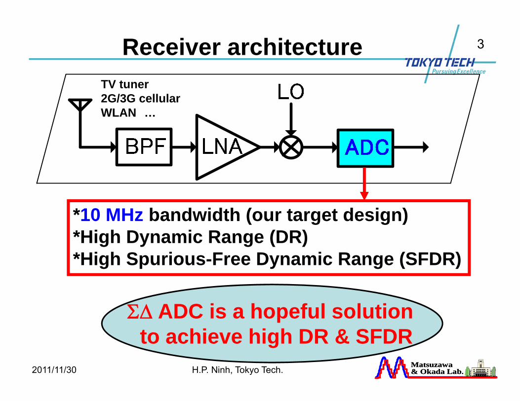
3Receiver architectureTV tuner2G/3G cellularWLAN …
*10 MHz bandwidth (our target design)*High Dynamic Range (DR)*High Spurious-Free Dynamic Range (SFDR)
ΣΔ ADC is a hopeful solution
Matsuzawa& Okada Lab.Matsuzawa& Okada Lab.2011/11/30 H.P. Ninh, Tokyo Tech.
to achieve high DR & SFDR
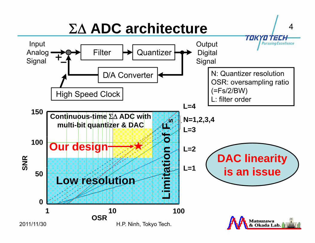
4ΣΔ ADC architecture
N: Quantizer resolution
L=4
N: Quantizer resolutionOSR: oversampling ratio (=Fs/2/BW)L: filter order
L=3
L=4
N=1,2,3,4150
of F
sContinuous-time ΣΔ ADC with multi-bit quantizer & DAC
SNR
L=1
L=2100
DAC linearity i iat
ion
oOur design
S L=150 is an issue
Low resolutionLi
mita
Matsuzawa& Okada Lab.Matsuzawa& Okada Lab.2011/11/30 H.P. Ninh, Tokyo Tech.
1 10 1000
OSR
L
5
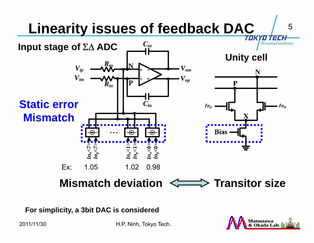
Ci
Linearity issues of feedback DACI t t f ΣΔ ADC
VipRin
Cin
Vom
V+ -N
Input stage of ΣΔ ADCUnity cell
Rin
Cin
VopVim - +P
Static error inStatic errorMismatch
Inp<
0>In
n<0>
Inp<
1>In
n<1>
Inp<
7>In
n<7>
1 05 0 981 02Ex: 1.05 0.981.02Ex:
Mismatch deviation Transitor size
Matsuzawa& Okada Lab.Matsuzawa& Okada Lab.2011/11/30 H.P. Ninh, Tokyo Tech.
For simplicity, a 3bit DAC is considered
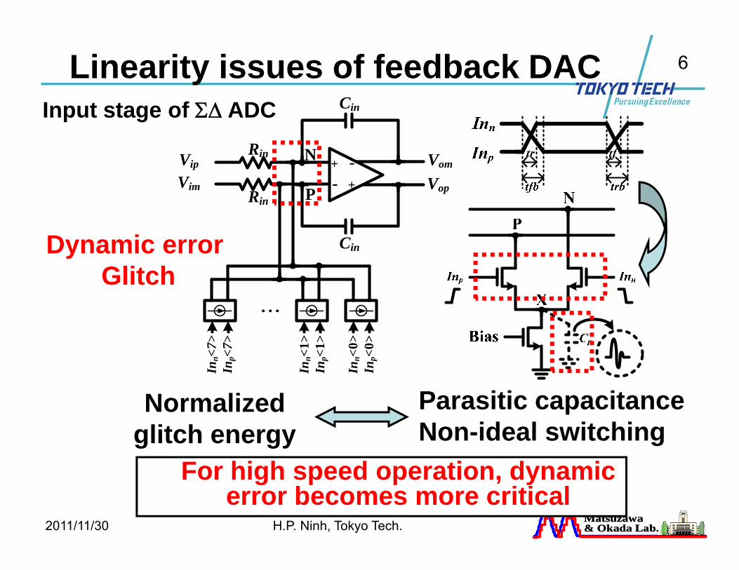
6Linearity issues of feedback DACCiI t t f ΣΔ ADC
VipRin
Cin
Vom
V+ -N
Input stage of ΣΔ ADC
Dynamic error
Rin
Cin
VopVim - +P
Dynamic error Glitch
in
Inp<
0>In
n<0>
Inp<
1>In
n<1>
Inp<
7>In
n<7>
P iti itNormalized glitch energy
Parasitic capacitanceNon-ideal switching
F hi h d ti d iMatsuzawa& Okada Lab.Matsuzawa& Okada Lab.2011/11/30 H.P. Ninh, Tokyo Tech.
For high speed operation, dynamic error becomes more critical
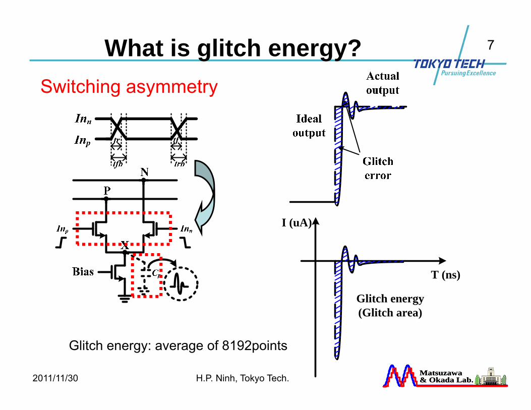
7What is glitch energy?Switching asymmetry
I (uA)
T (ns)
Glitch energy(Glitch area)
Matsuzawa& Okada Lab.Matsuzawa& Okada Lab.2011/11/30 H.P. Ninh, Tokyo Tech.
Glitch energy: average of 8192points
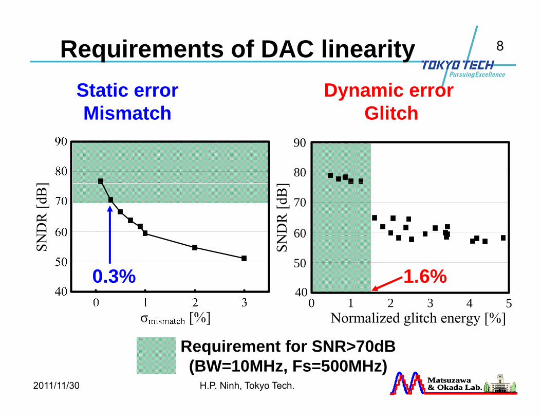
8Requirements of DAC linearityStatic errorMismatch
Dynamic error Glitch
80
90
60
70
40
50
60
0.3% 1.6%0 1 2 3
404 5
R i t f SNR 70dB
Matsuzawa& Okada Lab.Matsuzawa& Okada Lab.2011/11/30 H.P. Ninh, Tokyo Tech.
Requirement for SNR>70dB(BW=10MHz, Fs=500MHz)
9Outline
• MotivationMotivation• Proposed one-element-shifting
(OES) DEM method(OES) DEM method• Implementation and measurement
ltresults• Conclusion
Matsuzawa& Okada Lab.Matsuzawa& Okada Lab.2011/11/30 H.P. Ninh, Tokyo Tech.
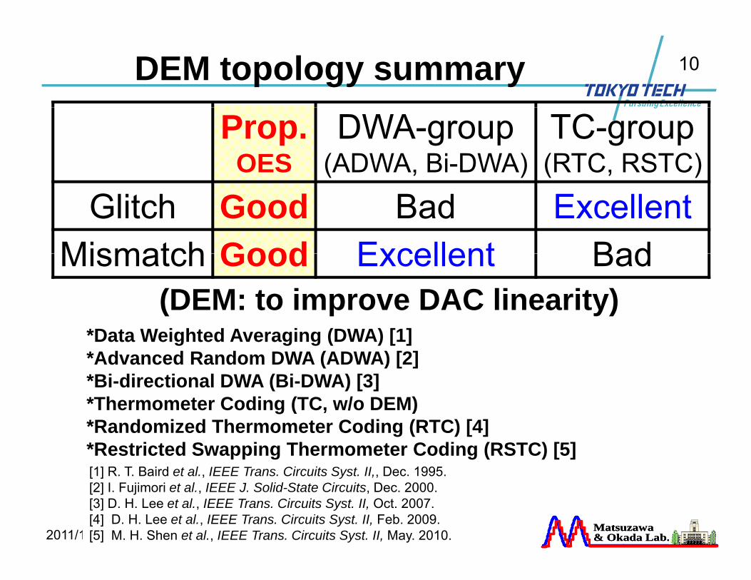
10DEM topology summaryProp.
OESDWA-group
(ADWA, Bi-DWA)TC-group(RTC, RSTC)
Glitch Good Bad ExcellentMismatch Good Excellent BadMismatch Good Excellent Bad
(DEM: to improve DAC linearity)*Data Weighted Averaging (DWA) [1]*Advanced Random DWA (ADWA) [2]*Bi-directional DWA (Bi-DWA) [3]*Th t C di (TC / DEM)*Thermometer Coding (TC, w/o DEM)*Randomized Thermometer Coding (RTC) [4]*Restricted Swapping Thermometer Coding (RSTC) [5][1] R T Baird et al IEEE Trans Circuits Syst II Dec 1995
Matsuzawa& Okada Lab.Matsuzawa& Okada Lab.2011/11/30 H.P. Ninh, Tokyo Tech.
[1] R. T. Baird et al., IEEE Trans. Circuits Syst. II,, Dec. 1995.[2] I. Fujimori et al., IEEE J. Solid-State Circuits, Dec. 2000.[3] D. H. Lee et al., IEEE Trans. Circuits Syst. II, Oct. 2007.[4] D. H. Lee et al., IEEE Trans. Circuits Syst. II, Feb. 2009.[5] M. H. Shen et al., IEEE Trans. Circuits Syst. II, May. 2010.
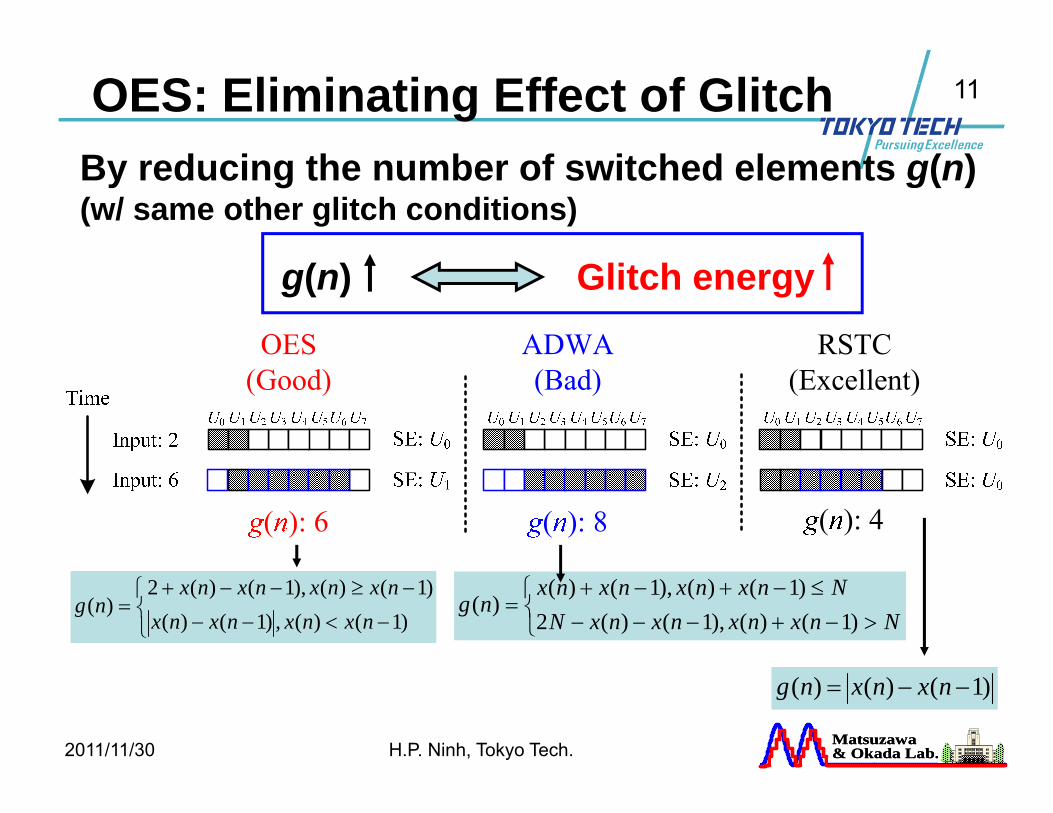
11OES: Eliminating Effect of GlitchBy reducing the number of switched elements g(n)(w/ same other glitch conditions)
g(n) Glitch energy
⎩⎨⎧
>−+−−−≤−+−+
=NnxnxnxnxN
Nnxnxnxnxng
)1()(),1()(2)1()(),1()(
)(⎩⎨⎧
−<−−
−≥−−+=
)1()(,)1()()1()(),1()(2
)(nxnxnxnx
nxnxnxnxng
Matsuzawa& Okada Lab.Matsuzawa& Okada Lab.2011/11/30 H.P. Ninh, Tokyo Tech.
)1()()( −−= nxnxng
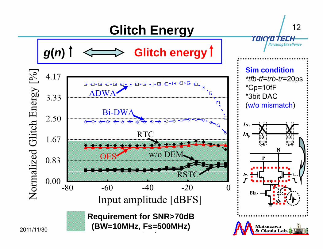
12Glitch Energyg(n) Glitch energy
Sim condition*tfb tf trb tr 20ps*tfb-tf=trb-tr=20ps*Cp=10fF*3bit DAC (w/o mismatch)( )
Matsuzawa& Okada Lab.Matsuzawa& Okada Lab.2011/11/30 H.P. Ninh, Tokyo Tech.
Requirement for SNR>70dB(BW=10MHz, Fs=500MHz)
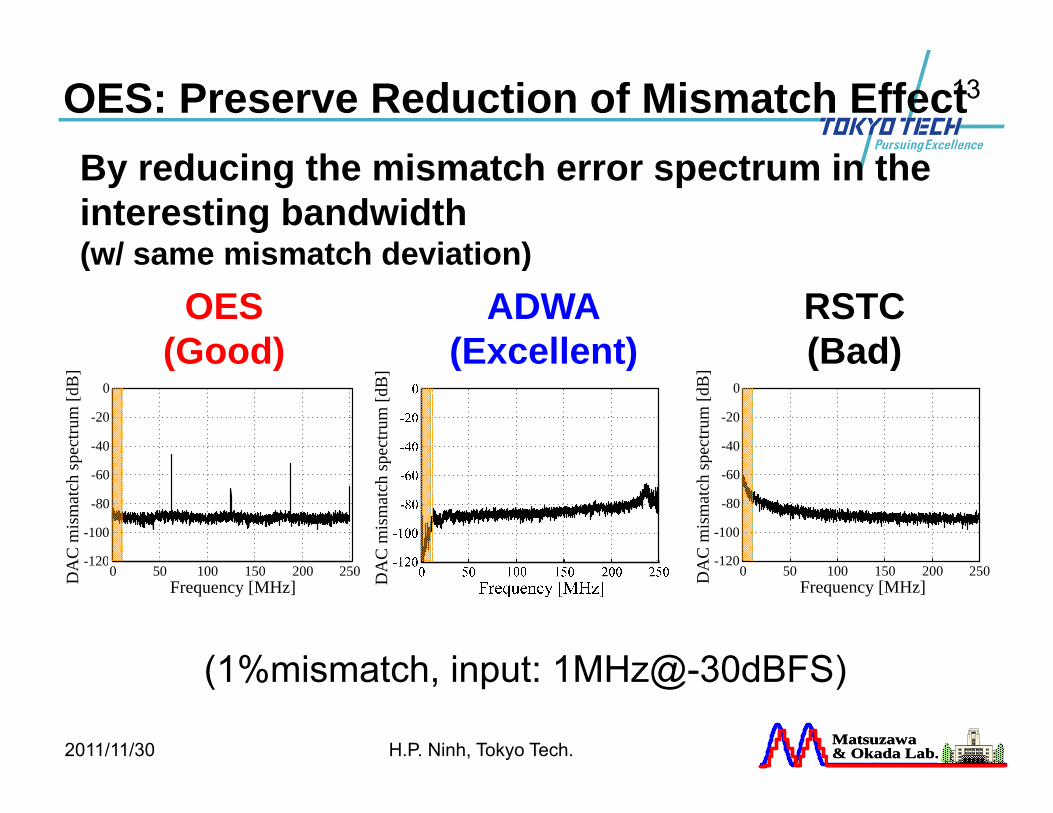
13OES: Preserve Reduction of Mismatch Effect By reducing the mismatch error spectrum in the interesting bandwidth(w/ same mismatch deviation)(w/ same mismatch deviation)
OES(Good)
ADWA(Excellent)
RSTC(Bad)
pect
rum
[dB
]
-40
-20
0
pect
rum
[dB
]
-40
-20
0
pect
rum
[dB
]
(Good) (Excellent) (Bad)A
C m
ism
atch
sp
120
-100
-80
-60
AC
mis
mat
ch sp
120
-100
-80
-60
AC
mis
mat
ch sp
DA
Frequency [MHz]50 100 150 200 250
-120
DA 0
Frequency [MHz]50 100 150 200 2500
-120
DA
(1%mismatch input: 1MHz@ 30dBFS)
Matsuzawa& Okada Lab.Matsuzawa& Okada Lab.2011/11/30 H.P. Ninh, Tokyo Tech.
(1%mismatch, input: 1MHz@-30dBFS)
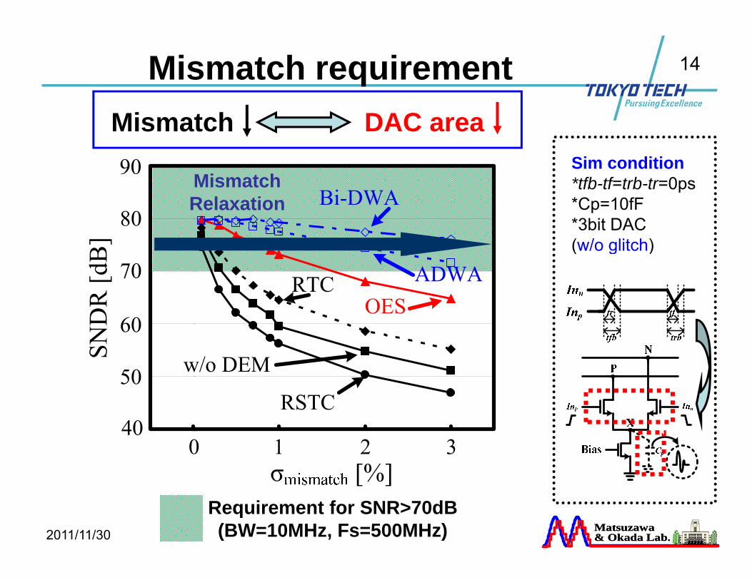
14Mismatch requirementMismatch DAC area
MismatchSim condition*tfb tf trb tr 0psMismatch
Relaxation*tfb-tf=trb-tr=0ps*Cp=10fF*3bit DAC (w/o glitch)( g )
Matsuzawa& Okada Lab.Matsuzawa& Okada Lab.2011/11/30 H.P. Ninh, Tokyo Tech.
Requirement for SNR>70dB(BW=10MHz, Fs=500MHz)
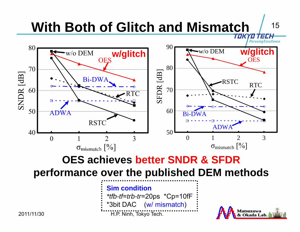
15With Both of Glitch and Mismatch 90
80OES
w/o DEMw/glitch w/glitch
70RTCRSTC
50
60
ADWA
Bi-DWA
OES achieves better SNDR & SFDR
50
mismatch
0 1 2 3
OES achieves better SNDR & SFDRperformance over the published DEM methods
Sim condition
Matsuzawa& Okada Lab.Matsuzawa& Okada Lab.2011/11/30 H.P. Ninh, Tokyo Tech.
Sim condition*tfb-tf=trb-tr=20ps *Cp=10fF*3bit DAC (w/ mismatch)
16Outline
• BackgroundBackground• Proposed one-element-shifting
(OES) DEM method(OES) DEM method• Implementation and measurement
ltresults• Conclusion
Matsuzawa& Okada Lab.Matsuzawa& Okada Lab.2011/11/30 H.P. Ninh, Tokyo Tech.
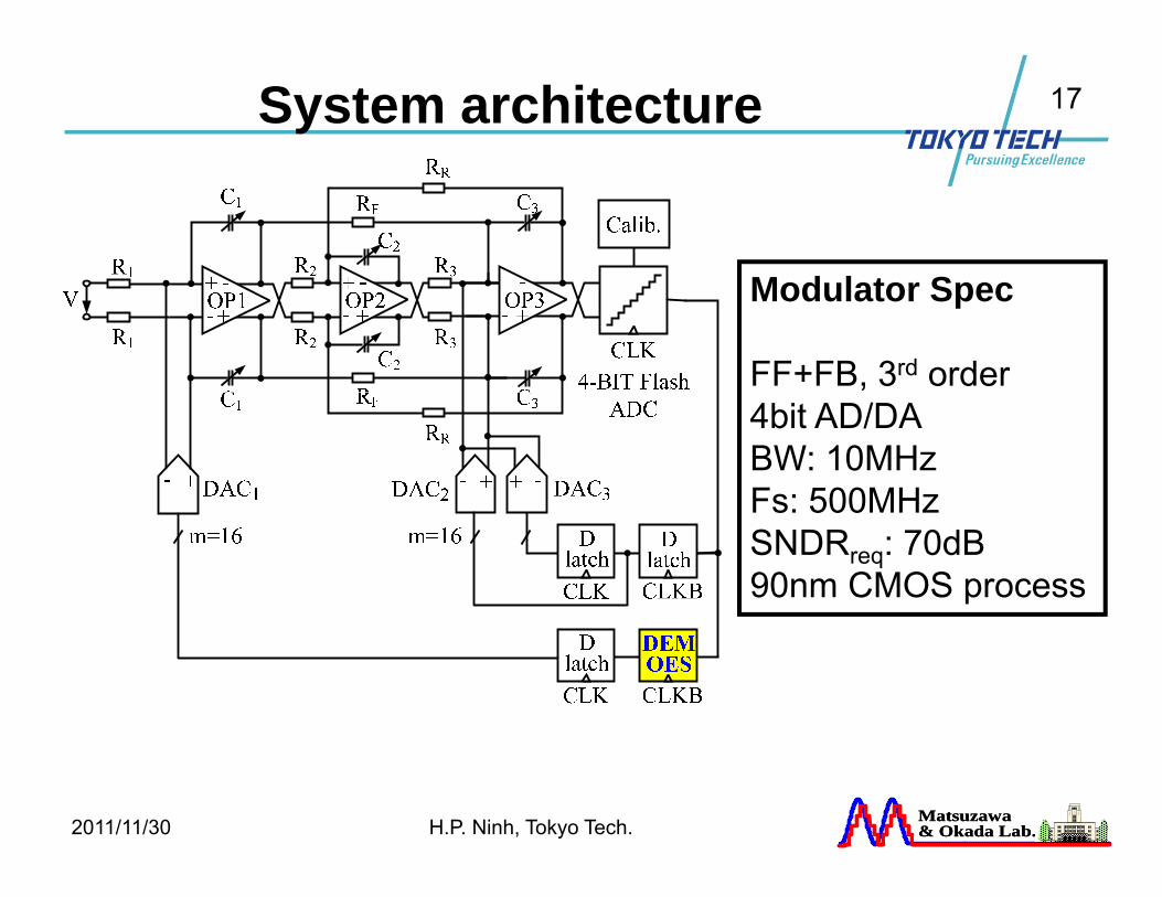
17System architecture
M d l t SModulator Spec
FF+FB, 3rd order4bit AD/DABW: 10MHzFs: 500MHzFs: 500MHzSNDRreq: 70dB90nm CMOS process
Matsuzawa& Okada Lab.Matsuzawa& Okada Lab.2011/11/30 H.P. Ninh, Tokyo Tech.
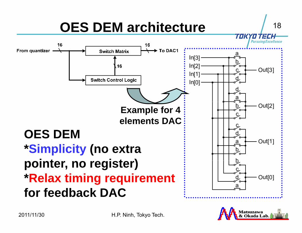
18OES DEM architecture
OES DEM
Example for 4 elements DAC
OES DEM*Simplicity (no extra
i t i t )pointer, no register)*Relax timing requirementf f db k DAC
Matsuzawa& Okada Lab.Matsuzawa& Okada Lab.2011/11/30 H.P. Ninh, Tokyo Tech.
for feedback DAC
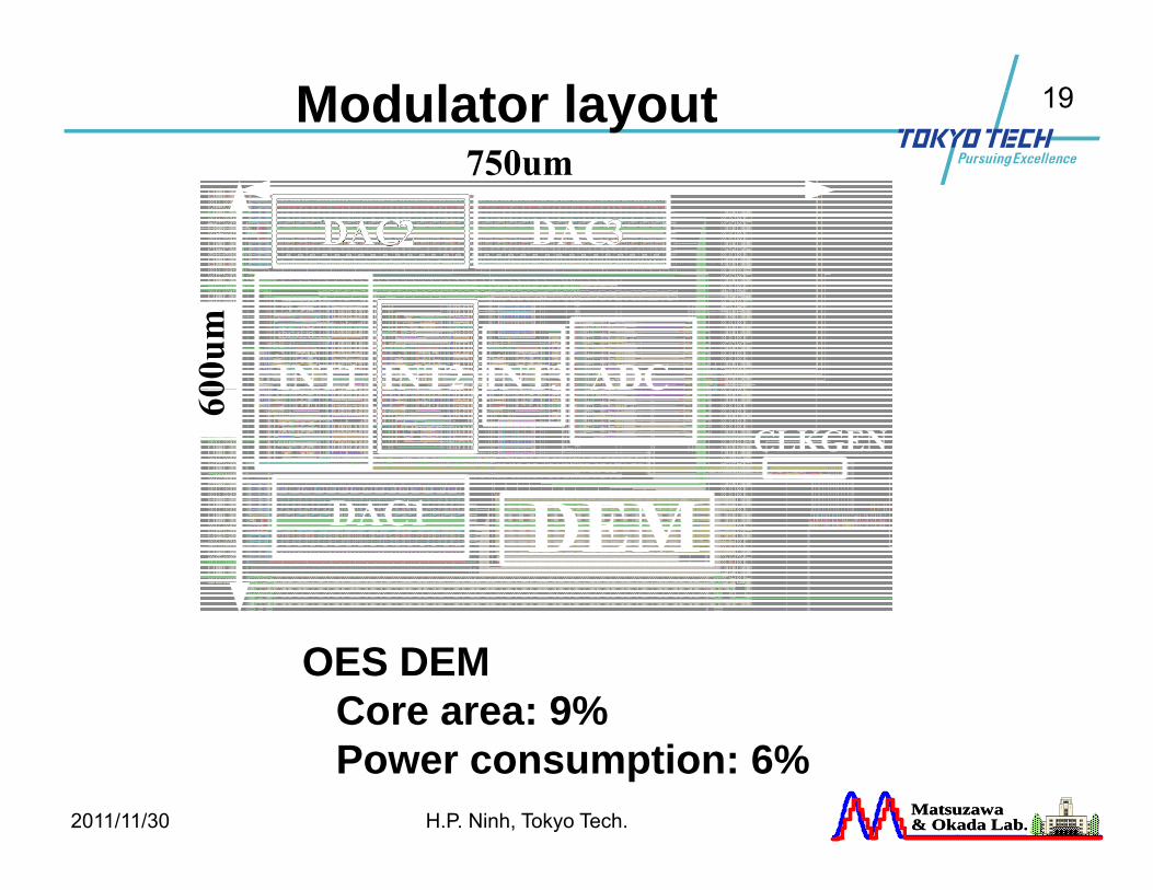
19Modulator layout
OES DEM Core area: 9%
Matsuzawa& Okada Lab.Matsuzawa& Okada Lab.2011/11/30 H.P. Ninh, Tokyo Tech.
Power consumption: 6%
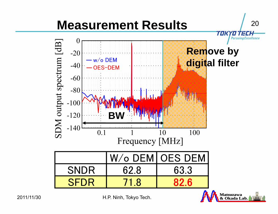
20Measurement Results
w/o DEM
OES DEM
Remove by digital filter
OES-DEMg
BW
W/o DEM OES DEMSNDR 62.8 63.3
Matsuzawa& Okada Lab.Matsuzawa& Okada Lab.2011/11/30 H.P. Ninh, Tokyo Tech.
SFDR 71.8 82.6
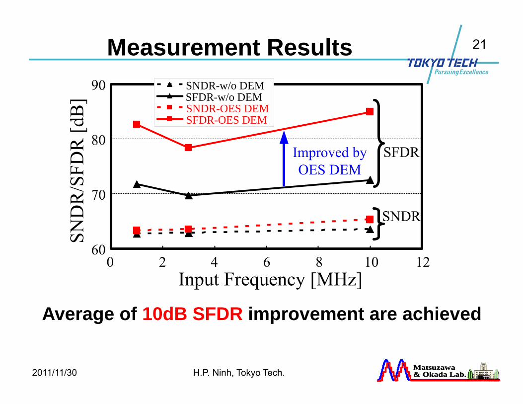
21Measurement ResultsSNDR-w/o DEMSFDR-w/o DEMSNDR-OES DEMSFDR-OES DEM
Average of 10dB SFDR improvement are achieved
Matsuzawa& Okada Lab.Matsuzawa& Okada Lab.2011/11/30 H.P. Ninh, Tokyo Tech.
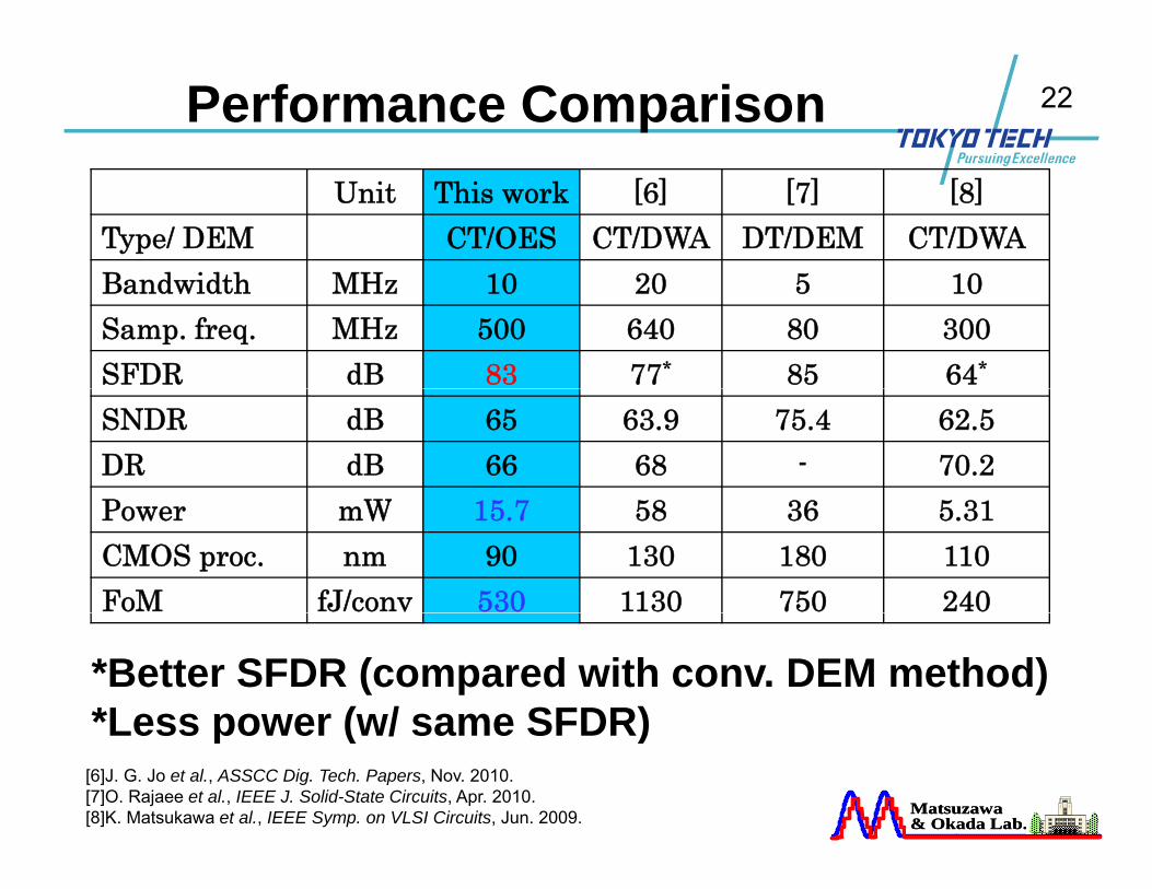
22Performance ComparisonUnit This work [6] [7] [8]
Type/ DEM CT/OES CT/DWA DT/DEM CT/DWAB d idth MH 10 20 5 10Bandwidth MHz 10 20 5 10Samp. freq. MHz 500 640 80 300SFDR dB 83 77* 85 64*
SNDR dB 65 63.9 75.4 62.5DR dB 66 68 - 70.2P W 15 7 58 36 5 31Power mW 15.7 58 36 5.31CMOS proc. nm 90 130 180 110FoM fJ/conv 530 1130 750 240
*Better SFDR (compared with conv. DEM method)*Less power (w/ same SFDR)
Matsuzawa& Okada Lab.Matsuzawa& Okada Lab.2011/11/30 H.P. Ninh, Tokyo Tech.
Less power (w/ same SFDR)[6]J. G. Jo et al., ASSCC Dig. Tech. Papers, Nov. 2010.[7]O. Rajaee et al., IEEE J. Solid-State Circuits, Apr. 2010.[8]K. Matsukawa et al., IEEE Symp. on VLSI Circuits, Jun. 2009.
23Outline
• BackgroundBackground• Proposed one-element-shifting
(OES) DEM method(OES) DEM method• Implementation and measurement
ltresults• Conclusion
Matsuzawa& Okada Lab.Matsuzawa& Okada Lab.2011/11/30 H.P. Ninh, Tokyo Tech.
24Conclusion
• Proposed OES DEM method substantially suppresses the both effects of mismatchsuppresses the both effects of mismatch and glitch.
• ΣΔ modulator using OES DEM achieves• ΣΔ modulator using OES DEM achieves 83dB SFDR and 10dB improvementcompared to no DEMcompared to no DEM.
• Simplicity and effectiveness of the OES technique makes it very attractive andtechnique makes it very attractive and prefer for cost and power considerations.
Matsuzawa& Okada Lab.Matsuzawa& Okada Lab.2011/11/30 H.P. Ninh, Tokyo Tech.
25Acknowledgments
This work was supported by CREST, JST, pp yVLSI Design and Education Center (VDEC), the University of Tokyo in collaboration with y yCadence Design Systems. The authors also acknowledge Berkeley Design Automation for g y gthe use of the Analog FastSPICE (AFS) Platform.
Matsuzawa& Okada Lab.Matsuzawa& Okada Lab.2011/11/30 H.P. Ninh, Tokyo Tech.
26Reference[1] R. T. Baird and T. S. Fiez, “Linearity enhancement of multibit ∆Σ A/D and D/A converters using
data weighted averaging,” IEEE Trans. Circuits Syst. II, Analog Digit. Signal Process., vol. 42, no. 12, pp. 753–762, Dec. 1995.
[2] I. Fujimori, L. Longo, A. Hairapetian, K. Seiyama, S. Kosic, J. Cao, and S. L. Chan, “A 90-dB SNR 2.5-MHz output-rate ADC using cascaded multibit delta-sigma modulation at 8X oversampling ratio,” IEEE J. Solid-State Circuits, vol. 35, no. 12, pp. 1820–1828, Dec. 2000.
[3] D. H. Lee, and T. H. Kuo, “Advancing data weighted averaging technique for multi-bit sigma–delta modulators ,” IEEE Trans. Circuits Syst. II, Exp. Briefs, vol. 54, no. 10, pp. 838–842, Oct. 2007.
[4] D. H. Lee, T. H. Kuo, and K. L. Wen, “Low-cost 14-bit current-steering DAC with a randomized thermometer-coding method,” IEEE Trans. Circuits Syst. II, Exp. Briefs, vol. 56, no. 2, pp. 137–141 Feb 2009141, Feb. 2009.
[5] M. H. Shen, J. H. Tsai, and P. C. Huang, “Random swapping dynamic element matching technique for glitch energy minimization in current-steering DAC,” IEEE Trans. Circuits Syst. II, Exp. Briefs, vol. 57, no. 5, pp. 369–373, May. 2010.
[6] J. G. Jo, J. Noh, and C. Yoo, “A 20MHz bandwidth continuous-time Σ∆ modulator with jitter immunity improved full-clock period SCR (FSCR) DAC and high speed DWA ” ASSCC Dig Techimmunity improved full-clock period SCR (FSCR) DAC and high speed DWA, ASSCC Dig. Tech. Papers, pp. 1-4, Nov. 2010.
[7] O. Rajaee, T. Musah, N. Maghari, S. Takeuchi, M. Aniya, K. Hamashita, and U. K. Moon, “Design of a 79 dB 80 MHz 8X-OSR Hybrid Delta-Sigma Pipelined ADC,” IEEE J. Solid-State Circuits, Vol. 45, No. 4, pp. 719-730, Apr. 2010.
[8] K. Matsukawa, Y. Mitani, M. Takayama, K. Obata, S. Dosho and A. Matsuzawa, “A 5th-Order[8] K. Matsukawa, Y. Mitani, M. Takayama, K. Obata, S. Dosho and A. Matsuzawa, A 5th Order Delta-Sigma Modulator with Single-Opamp Resonator,” IEEE Symp. on VLSI Circuits, pp. 68-69, Jun. 2009.
Matsuzawa& Okada Lab.Matsuzawa& Okada Lab.2011/11/30 H.P. Ninh, Tokyo Tech.
27
Thank you!!!
Matsuzawa& Okada Lab.Matsuzawa& Okada Lab.2011/11/30 H.P. Ninh, Tokyo Tech.