Embed Size (px)
Citation preview

A wide linear dynamic range image sensor
based on asynchronous self-reset and tagging
of saturation events
Juan A. Lenero-Bardallo, R. Carmona-Galan and A. Rodrıguez-Vazquez
Abstract
We report a High Dynamic Range (HDR) image sensor with linear response that overcomes some of
the limitations of sensors with pixels with self-reset operation. It operates similarly to an Active Pixel
Sensor (APS), but its pixels have a novel asynchronous event-based overflow detection mechanism.
Whenever pixels voltage at the integration capacitance reaches a programmable threshold, pixels self-
reset and send out asynchronously an event indicating it. At the end of the integration period, the voltage
at the integration capacitance is digitized and readout. Combining this information with the number of
events fired by each pixel, it is possible to render linear HDR images. Event operation is transparent to
the final user. There is not a limitation for the number of self-resets of each pixel. The output data format
is compatible with frame-based devices. The sensor was fabricated in the AMS 0.18µm HV technology.
A detailed system description and experimental results are provided in the article. The sensor can render
images with intra-scene dynamic range up to 130dB with linear outputs. Pixels pitch is 25µm. Sensor
power consumption is 58.6mW.
Keywords: Image sensor, HDR, Event, AER, High Dynamic Range, Linear response, Event, Octopus
retina.
J. A. Lenero-Bardallo is with the University of Cadiz, Cadiz, Spain, (E-mail: [email protected]). R. Carmona-Galan,and A. Rodrıguez-Vazquez are with the Institute of Microelectronics of Seville, CSIC-Universidad de Sevilla, Sevilla 41004,Spain (E-mails: [email protected]; [email protected]).
This work was supported in part by the University of Cadiz research program under grant PR2016-072, in part by the SpanishMinistry of Economy and Competitiveness under Grant TEC2015-66878-C3-1-R, Co-Funded by ERDF-FEDER, in part byJunta de Andalucıa CEICE under Grant TIC 2012-2338 (SMARTCIS-3D), and in part by ONR under Grant N000141410355(HCELLVIS).
2
I. INTRODUCTION
High Dynamic Range (HDR) operation is desired for many applications with image sensors:
surveillance, quality imaging, drone vision, etc. In general, it is always mandatory in scenarios
without controlled illumination conditions. In that sense, designers try to maximize the dynamic
range, when designing image sensors, to amplify its range of applicability.
The classic Active Pixel Sensor (APS) has a limited dynamic range. For a fixed integration
time, the lowest lower photocurrent value that can be sensed is limited by the quantization noise
or the read noise of the analog-to-digital-converter. The largest photocurrent value is usually
limited by the full well capacity. By increasing the integration time, it is possible to sense
lower photocurrent values, but the highest photocurrent that can be gauged will be lower. If the
integration time is decreased, it will be possible to operate with higher illumination, but precision
within lower illuminated areas will be lost. Therefore the dynamic range is inherently limited
by the sensor and cannot be extended by globally adjusting the integration time. Typically, APS
sensors DR is limited to values below 70dB [1]. If we compare this feature to the performance
of the human eye it is sensibly worse. Our eyes can sense images with an intra-scene dynamic
range over six decades [2]. Typical natural scenes can reach a DR of 120dB [1]. Therefore there
is a need of HDR operation to render images with a precision close to our human perception.
There are several techniques to extend the dynamic range [1], [3], [4]. Maybe the most
popular is to capture images with multiple integration times and then combine them [5]–[9].
This approach has expensive requirements regarding computational load, hardware, and power
consumption. Firstly, dedicated algorithms have to be programmed to combine the different
images (irradiance maps) and render the final HDR photo [10]. Before combining the different
frames they have to be captured as individual images, and stored on memory. Thus, frame rate
will be lowered, and the power consumption increased. Furthermore, multiple captures with
misaligned integration times can generate inexistent edges and distort the interpretation of the
scene [11].
March 1, 2017 DRAFT

3
Another option to extend the dynamic range is to use Tone Mapping (TM) algorithms [4],
[12], [13]. Based on image histograms, grey levels are assigned with more precision to the
values that are more frequent in the visual scene. Thus, there is a non-lineal relation between
the pixel photocurrents and the grey levels assigned to each pixel. Resulting HDR images have
a low number of bits to encode illumination. There are sensors that implement TM algorithms
on chip [13]. The approach produces quality HDR images. Unfortunately, all illumination levels
are not encoded with the same accuracy and there is a loss of information. The choose of the
TM curves is not trivial, and conditions the quality of the final image. Hence, the process of
tone mapping is not reversible once one frame has been rendered implementing this technique
on chip. Moreover, in machine vision applications where precise contrast information or high
speed is required, these calculation based methods can be inadequate [1].
More recently, several event-based image sensors with inherent HDR operation have been
reported [14]–[19]. They try to mimic biological systems. They usually employ a logarithmic
compression of the illumination values to extend the dynamic range. They also try to perform
same kind of in-pixel processing; typically spatio-temporal contrast detection. Their approach
is effective, but their event-based description of the scene is not easily compatible with the
most widely employed frame-based displays and conventional frame-based image processing
algorithms, like Viola Jones [20]. Many application just require to encode intensity levels of the
visual scene.
In this article, we describe in detail a novel concept of image sensor with a high dynamic
range linear output. A preliminary theoretical circuit analysis was already advanced [21]. The
sensor combines classic APS pixel operation with event-based overflow detection. Its pixels never
overflow during the integration time. Every time that the voltage at the integration capacitance
reaches a limit, the pixel resets itself and continues integrating charge again. Events are sent out
to indicate how many times a pixel has overflowed. Ideally, high illuminated pixels will never be
overexposed. The selection of the integration time determines the minimum illumination values
March 1, 2017 DRAFT

4
that can be sensed. Knowing the number of events (if any) associated to each pixel and the
digitized voltage at the end of the integration period, it is possible to obtain digital words which
value is proportional to illumination. Sensor outputs are compatible with frame-based displays
and processing algorithms. Event operation is totally transparent. All the illumination values are
encoded with the same precision. The user can trade between frame rate, the amount of memory
dedicated to store the event information, and the maximum intra-scene dynamic range that can
be sensed.
The pixel self-resetting mechanism is not new and was already proposed by other authors
[22]–[25], just to mention but a few. It leads to pixels with linear output, high SNR, and high
dynamic range. However, reported pixels require in-pixel counters to store the number of pulses.
This limits the number of pixel resets that can be sensed. Extra time is required to readout the in-
pixel memories after the integration time, lowering the frame rate. To the best of our knowledge,
image sensors that combine APS readout with a self-resetting mechanism, based on an Address
Event Representation (AER) [26], [27], high speed asynchronous arbitration scheme have not
been reported yet. With this new approach the number of times that a pixel can overflow is not
limited by a pixel memory. Low illumination values can be sensed with the APS readout. Large
illumination values are sensed activating an independent event-based data flow.
II. PIXEL OPERATION
A. Operation Principle
Fig. 1 shows the new pixel operation concept to extend the dynamic range. Pixel voltage at
the integration capacitance never overflows. If it reaches a voltage threshold, Vbot, the pixel will
reset itself and continue integrating charge again immediately after. Every time (if any) that the
integration voltage reaches the value Vbot, an event will be sent out of the chip. We will refer
in the article to the event data flow as the ”event readout”. At the end of the integration period
Tint, the voltage at the integration capacitance, Vint will be digitized, stored on a memory, and
send out the chip. We will denote this another output data flow as the ”APS readout”. Both
March 1, 2017 DRAFT
5
data flows are independent and can be merged to render high dynamic range images. The sensor
pixel output values will be proportional to their local illumination:
Iph ∝ (Vreset − Vint) + (Vreset − Vbot) · (#events) (1)
The intra-scene dynamic range of a visual scene can be defined as the ratio between the
highest and the lowest illumination values that can be sensed within the visual scene. It is
usually expressed in decibels as:
DR = 20 · log10(Iphmax
Iphmin
)(2)
If we represent the photocurrent values with binary words of Nbits, the dynamic range of the
sensor is given by
DR = 20 · log10(2Nbits
)= 20 · log10
(2(Nb+Ns)
)(3)
Nb is the resolution of the analog-to-digital-converter, and Ns is the number of bits dedicated
to store the number of times that a pixel has spiked.
The novelty of this image sensor over previous ones based on self-reset operation [22], [24], [25]
is that pixels over-flow events are not stored on in-pixel memories. We use AER communication
to transmit asynchronously the address of the pixels that overflow every time that this event
occurs. AER point to point communication scheme is depicted in Fig. 2. When the sender is
ready to send information and has granted access to the AER bus, a Request signal is sent
to the receiver. In our case, the senders will be the different pixels sharing the AER bus. The
receiver is a digital FSM that stores pixel addresses on a memory. Then, the pixel address is
placed on the shared AER bus. When the receiver has received the information, it sends back
an Acknowledge signal. For a detailed explanation of modern AER communication schemes and
their performance we refer the reader to read the Boahen’s work [26], [31]. Specific details about
March 1, 2017 DRAFT

6
the AER circuitry described in this paper can be found in the Hafliger’s PhD work [27].
B. New Pixel’s Concept
Fig. 3 displays the pixels schematics. On the left, there is circuitry to implement the classic
APS operation and readout. In the middle, there is an astable oscillator. It pulses with a frequency
that is proportional to the input photocurrent, performing a light to frequency conversion. On
the right, there is specific asynchronous circuitry that handles the event communication and
has been reported elsewhere [27]. We will refer it on the article as the AER (Address Event
Representation) logic. Whenever the voltage at the integration capacitance reaches the value
Vbot, the voltage Vph should be reseted as fast as possible to minimize the error introduced by
the reset operation. To avoid waiting for the acknowledgements signals to reset the integration
capacitance, events requests are stored on the capacitor C1 until they can be acknowledged. The
event handshaking cycle is under normal circumstances much faster (nanoseconds scale) that
the event output frequency (milliseconds scale), even under high illumination. Therefore, the
probability of spiking before a previous event request has not been attended is very low and, for
a preliminary circuit analysis, we will consider that the AER logic does not introduce any error
in the light sensing.
Fig. 4.(a) shows a timing chart with the pixel control signals. Initially, all the pixels are reset
simultaneously. Then, they integrate charge during Tint. During the integration period, pixels
that over-flow send events through the shared AER bus. At the end of the integration period,
the voltage Vint is stored. Then, different pixel rows (96 in this implementation) are read-out
sequentially and the different Vint voltages of each column are digitized and stored on a memory.
In Fig. 4.(b) there is a timing chart with the pixel signals involved in the asynchronous event
communication during Tint. Every time that a pixel overflow happens, the signals involved in
the AER communication are activated as it is depicted. On the bottom of 4.(b), there are the
external signals involved in the entire pixel array communication. Since the AER bus is shared
March 1, 2017 DRAFT

7
by all the pixels, there is arbitration circuitry to assure that only one pixel have access the bus
at some moment (see details in Section III-A). The amount of time required to transmit one
event, Thandshake, depends on the bus congestion. Typical values are Thandshake=100-200ns. If
the sensor is not exposed to intense light, the handshaking cycle is much lower than the pixels
oscillation period.
Let us analyze the astable oscillator. It generates pulses with a period that is approximately:
T =C · (Vreset − Vbot)
Iph+ Td + Treset ≈
C ·∆VIph
(4)
Td ≈25ns is the controlled delay introduced to make the oscillator stable. Treset ≈400ns is the
amount of time required by the transistor Mp3 of Fig. 3 to reset the integration capacitance with
∆V =4V. For simplicity, for a preliminary circuit analysis, its value can be neglected because it
is much lower than the oscillation period. Under high illumination, pixel spiking frequencies are
in milliseconds scale. Let us denote the frame rate as FR. For a given value of the integration
period depicted in Figure 1 (Tint =1/FR), the minimum detectable photocurrent provokes a
voltage decrement of 1LSB of the analog-to-digital-converter, i.e.:
Iphmin=C ·∆V · FR
2Nb(5)
Therefore, combining Equations (2) and (5), the dynamic range expressed as a function of the
maximum photocurrent that can be measured (Iphmax) and the frame rate (FR) is:
DR = 20 · log10(
2Nb · Iphmax
FR · C ·∆V
)(6)
One practical limitation of our approach is that the arbitration system can handle a maximum
output event rate MAXBR = 1/Thandshacking that depends on the amount of time required by
the arbitration logic to complete the event communication cycle depicted in Figures
March 1, 2017 DRAFT

8
M ·N · fmax < MAXBR (7)
fmax is the maximum average spiking frequency when the array is illuminated uniformly. It
depends on ∆V . For a given illumination value, we can control the global event rate by adjusting
∆V . We can lower the event rate by increasing ∆V = Vreset−Vbot = VDD−Vbot. In our particular
case, we have implemented a pixel matrix in the AMS 0.18µm HV standard technology that
offers transistors with thicker gate oxide that can reach voltages up to 5V. Hence pixels use this
transistors to minimize the event rate, maximizing the value of ∆V .
Let us analyze the error introduced by the proposed self-resetting mechanism. The error is
mainly due to the the amount of time needed to reset of the integration capacitance, Treset. The
controlled delay at the output of the astable oscillator (Td) also contributes. Such errors are
approximately Td ≈ 25ns and Treset ≈400ns (see Equation (4)). In the worst case, during the
integration period Tint, a pixel can spike a maximum of 2Ns times. Hence the total accumulated
error will be TdT = (Td + Treset) · 2Ns . The relative error is ε =TdT
Tint= (Td + Treset) · 2Ns · FR.
If we assume a frame rate FR=25frames/s and, Ns=12bits, the maximum possible relative error
introduced by the self-reset operation will be ε=4.3%. In real operation scenarios, all the pixels
will not be exposed to the maximum illumination value. Therefore the expected error will be
lower than ε. By lowering the frame rate, the error will be lower too. By increasing the width
of transistor Mp3 in Fig. 3, Treset will be reduced. The penalties are more area consumption
and higher transistor leakage. This error analysis is valid in all the scenarios where we tested
the sensor. In the particular case of heavy AER bus congestion due to high event activity, the
arbitration periphery may introduce additional errors due to event loss. This effect will be shown
with experimental data in Section IV-C.
March 1, 2017 DRAFT

9
C. Trade-offs between dynamic range and frame rate
The dependence between the frame rate and the dynamic range is governed by Equation
(6). Iphmax is the maximum photocurrent that we can measure without saturating the arbitration
periphery. Combining Equations (7) and (4), it is possible to express Iphmax as a function of the
maximum average spiking frequency, fmax, that the sensor can process:
Iphmax = fmax · C ·∆V =MAXBR · C ·∆V
M ·N · α(8)
α is a parameter that indicates the percentage of pixels that are exposed to Iphmax . If α = 1, it
means that all the pixels are exposed to Iphmax . This situation is very pessimistic. In real scenes
with large intra-dynamic range, α will be lower than one. Combining Equations (6) and (8), it
is possible to express the dependence between the frame rate and the dynamic range:
DR = 20 · log10(
2Nb ·MAXBR
FR ·M ·N · α
)(9)
As long as the number of bits dedicated on memory (Nb + Ns) to store the intensity levels
is high enough, the dynamic range only depends on the maximum event rate that the peripheral
circuitry can cope, the total number of pixels, and the frame rate. Fig. 17 displays such depen-
dence for different values of α. Thus, there is a trade-off between the maximum event rate that
the sensor can handle, dynamic range, and frame rate.
III. SYSTEM LEVEL DESCRIPTION
Fig. 6 displays the complete system block diagram. In the middle, there is the pixel array
made up of 96×128 pixels. On the periphery, we have placed the event and APS readouts.
Both operate independently to generate two output data flows. The event flow occurs during
the integration time as it is depicted in Fig. 1. The APS readout is ready after the end of the
integration period.
March 1, 2017 DRAFT

10
A. Event readout circuitry
The circuitry dedicated to handle the event communication corresponds to the blocks plotted
on the top and right sides of Fig. 6. A detailed description of the AER blocks and its inter-
connectivity was presented by Hafliger [27]. It has also been reported elsewhere in other sensor
implementations [19], [28]. It can handle events rates up to 10Meps for pixels of different rows,
and 2Meps for pixels of the same row. In the chip implementation, row petitions are arbitered
first, with the peripheral circuitry of the right side. Afterwards, columns petitions are arbitered.
Finally, and external bus req signal and the address of the pixel that has spiked are sent out
of chip, until the bus ack signal is received. Thereafter, the next event is attended.
B. APS readout circuitry
The circuitry necessary to make the pixel operate as an APS CMOS pixel has been placed
on the left and the bottom of Fig. 6. The block on the left generates the row selection signals
(SEL) to select the different array rows sequentially for the analog-to-digital-conversion. Signals
RESET and STORE are activated globally. Hence, there is not a rolling shutter implemented.
On the bottom, there is the circuitry for the column parallel analog-to-digital-conversion. We
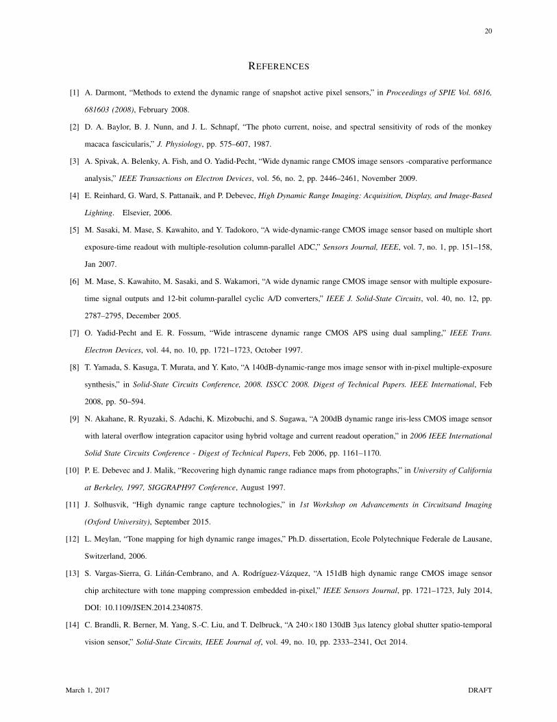
have implemented 128 column parallel ramp converters (see details on Fig. 7). Fig. 8 displays
the circuitry of the analog buffers that drives the DAC output voltages to the ramp converter
comparators. It is a simplified version of the wide range operation buffer proposed by Chih [29].
Furthermore a SRAM memory and shift registers were implemented on chip to save the APS
data and serialize it.
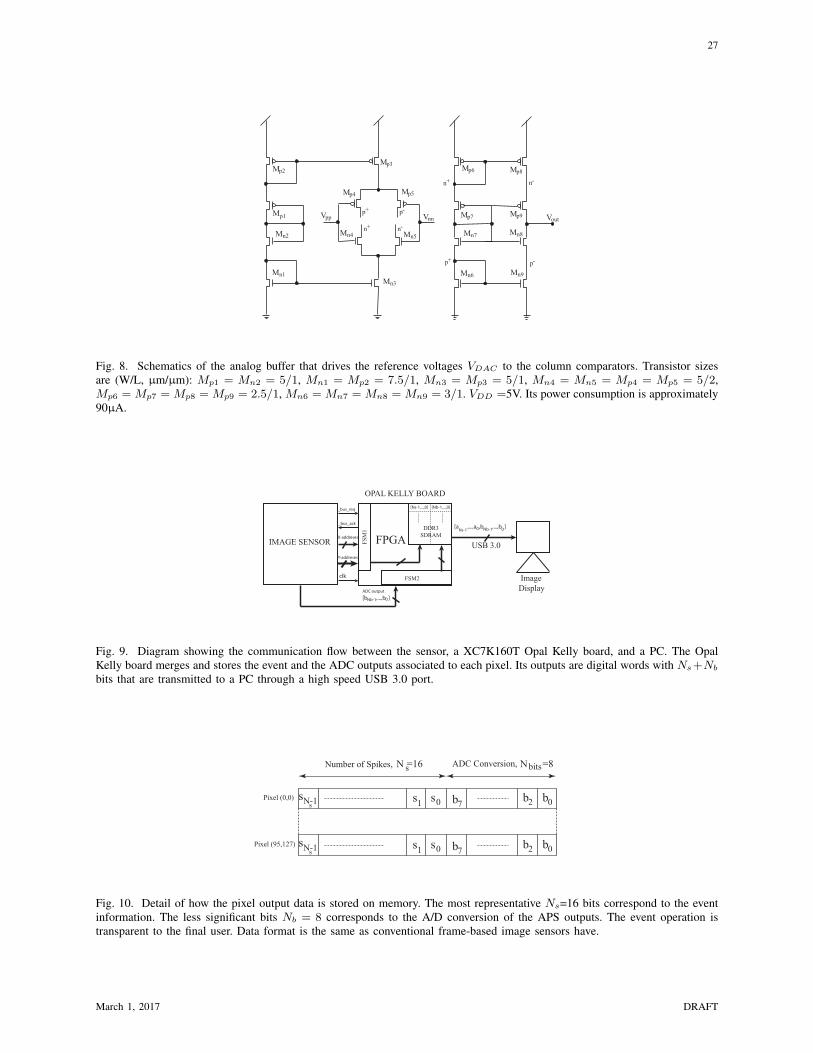
C. Off-chip data processing and storage
The output data flows are stored off-chip. There is an external XC7K160T Opal Kelly board
with a Kintex 7 FPGA that merges the event data flow and the digitized values of the readout
voltages at the end of the integration period. Fig. 9 shows the communication between the sensor
and Opal kelly board. It has an external DDR3 SDRAM memory to store frames at video rates
March 1, 2017 DRAFT
11
and higher. The FPGA internal clock is 200MHz. To process the data flow, two simple FSMs
were implemented on the FPGA. The first one handles the AER communication. The second
FSM reads and stores on memory the digitized pixel outputs (APS readout).
Fig. 10 depicts how pixel output data is stored on memory. The Ns=16 most representative
bits correspond to the number of events associated to each pixel. The less significant Nb =8bits
are the results of the A/D conversion of the APS outputs. The external memory has words of
32 bits. The value of Ns can be selected accordingly, taking into account the desired dynamic
range. With Ns + Nb =16+8=24bits, we set a theoretical maximum value for the intra-scene
dynamic range of 145dB.
IV. EXPERIMENTAL RESULTS
A. Experimental Setup and Interface
Fig. 11 (a-b) display the experimental setup. We designed a custom PCB to test the sensor and
a lens holder to hold the optics. The PCB is attached to an XEM7350 board. Since the sensor
event operation is independent to the frame-based operation, we have added to the sensor’s
PCB an IDC 40-pin connector, compatible with the USBAERmini datalogger that is commonly
extended among the AER community, [30] (see Fig. 11 (b) ).The interface can monitor the event
rate between frames, indicating if there is AER bus activity overload.
A custom interface (see Fig. 12) was programmed to test the sensor and display real-time
images. It has several operation modes to represent pixel intensities in different ways: color
scale, tone mapping, APS or event flow independently, etc.
B. Chip Microphotograph and Pixel Layout
The sensor was fabricated in the AMS 0.18µm HV technology. The technology has available
transistors with thick gate oxide that can operate up to 5V. Increasing ∆V , the event flow is
reduced and the accumulated error due to the self-resetting mechanism when events are sent out
too (see quantitative analysis in Section II). To save area and power consumption, the digital
March 1, 2017 DRAFT

12
circuitry was designed with nominal technology transistors that operate at 1.8V. Fig. 13 (a)-(b)
shows a chip microphotograph and the pixel layout.
C. Pixel Response to Illumination
Fig. 14 displays the sensor digital outputs (DN) versus the relative illumination values over
five decades. To take the measurements, a region of the sensor was illuminated with a very
bright light source. The rest of pixels were not exposed to light to avoid saturating the AER
communication circuitry. Neutral density filters were put in between the source and the sensor
to gauge the sensor outputs for different illumination values. The dependence between the
output code and illumination is highly linear in the entire operation range. We computed the
determination coefficient, obtaining r2 = 0.9961. Linearity is an advantage of this sensor over
other ones based on multiple exposition times or [5]–[9].
We studied the sensor response with low illumination, that is not entirely linear in these circum-
stances. The reason is that, in Fig. 3, the transistors Mn3, Mp2, and Mp3 current leakage and the
photodiode dark current are comparable to the photocurrent. That limitation is mainly imposed
by the technology. Hence, under very low illumination conditions the oscillation period can be
approximated by:
T =C ·∆V
Iph + Idark − Ileakage=
C · (VDD − Vbot)Iph + Idark − Ileakage
(10)
Where Idark is the photodiode dark current, and Ileakage is the current leakage due to transistors
Mn3, Mp2, and Mp3 in Fig. 3. To illustrate the effect, we measured under very low illumination
conditions (scene illumination was below 5lux) the transient voltage at the integration capacitance
of a test pixel, placed in one corner of the pixel array. Its integration capacitance was connected
to a scan buffer like the one depicted in Fig. 8. The pixel response is plotted in Fig. 15 in blue
trace. In red, we have plotted the expected behaviour. It can be seen that when the voltage at
the integration capacitance decreases, Ileakage has a higher impact on pixel performance leading
March 1, 2017 DRAFT

13
to a non-linear pixel response. Therefore, Ileakage depends on the value that is set by the user
to ∆V . The higher that ∆V is set, the higher that transistor leakage impact will be under low
illumination. If we decrease ∆V , the event rate will increase. Thus, there is a trade-off between
pixel linearity under low illumination and the event rate. Note that long integration times had to
be set to observe the situation depicted in Fig. 15. Pixel sensitivity could be enhanced by using
a dedicated CIS technology or by reducing the sensing capacitance. The penalty will be faster
event rates with the same illumination.
As we discussed in Section II-C, the arbitration delays of the peripheral circuitry limits the
maximum illumination values that can be sensed. Fig. 16 illustrates this effect. We illuminated
the whole sensor array with uniform light and we set an infinite integration time. The optics was
removed. Thus, all pixels were spiking with a frequency proportional to light. When the event
rate reaches a certain value, the dependence between event rate and illumination is not linear.
Some rows are the only ones that are able to send events out of the chip [27]. For this reason,
there is a fast growth on the dependence between illumination between the event rate when the
chip illuminace is close to 1klux. Events of pixels of the same rows can be arbitrated faster.
Then, the event rate cannot grow above a certain limit. Under these circumstances, not all the
pixels will be able to transmit events off-chip. Hence, the values of illumination related to such
pixel will not be correct. This is an unfavorable scenario. In practical situations, all the pixels
will not be exposed to high illumination simultaneously. Event activity can be monitored with
our interface. Faster AER arbitration circuitry that can reach 20Meps is also reported elsewhere
[26], [31].
D. Performance and Sample Images
A video showing some of the sensor capabilities is available [32]. Furthermore, Fig. 17 displays
several samples of HDR images taken with the sensor. For comparison purposes, on the first
column we show the same visual scene captured with a smartphone camera operating in HDR
March 1, 2017 DRAFT
14
mode. Its sensor was overexposed within the high illuminated regions of all the snapshots. On the
second column, we display the intensity levels measured with our sensor. We have employed a
linear thermal code to encode the linear sensor outputs. Using the three different color channels of
the display, there are available up to 24 bits to encode illumination values linearly. Although this
image representation is not close to our human perception of the visual scene, all the information
provided by the sensor is preserved. It can be useful to operate with the raw data provided by
the sensor in applications related to machine vision and pattern recognition. On the third column
of Fig. 17, we display images rendered with our sensor after processing its output data with
a TM algorithm. On the fourth column, we show the image histograms. On the right column,
we display the nonlinear law used to encoded grey levels. We assign more grey levels in the
resulting image to the illumination values that are more frequent in the visual scene. The user
has total freedom to customize the tone mapping curves. For the sake of simplicity, we have
defined curves based on a piecewise approximation. The computation of the dynamic range
of the sample images is straightforward according Equation (2). We measured intra-dynamic
ranges of 93dB, 85dB, 99dB, 125dB, and 126dB for the visual scenes (a), (f), (k), (q), and (v),
respectively. We used a 6mm C-mount lens to capture all the images, excepting image (s) that
was taken with a 25mm C-mount objective. An integration time, Tint =110ms was set to capture
all the snapshots. The maximum spiking frequency for an individual pixel that we could measure
was fpeak=55keps in the visual scene depicted in Fig 17.(v). Such pixel value corresponds to
the illumination of the bulb filament in a very specific localisation. If we take into account the
maximum event rate that can tolerate the AER bus, the maximum number of pixels that could
fire simultaneously at such speed is MAXBR/fpeak ≈182, that is a 1.5% the size of the pixel
array.
March 1, 2017 DRAFT

15
E. Practical Application Scenarios
The event output data flow is sent out the chip before the integration time is finished. Hence
it is possible to use this event information to display preliminary images before the final one is
rendered. Fig. 18 illustrates it. An integration time Tint = 110ms was set to capture a HDR scene.
Preceding images were rendered with the events received at different time stamps. Grey levels
were encoded using PDM modulation. Higher illuminated pixels can be displayed first, only a
few milliseconds after reseting the integration capacitance. On the right-bottom corner of Fig.
18, the resultant image is displayed. The sensor is potentially useful for application scenarios
where a fast preview of the visual scene is required before rendering detailed images.
In Fig. 19, the sensor is used to detect transient illumination variations of a very bright source
within a HDR scene that cannot be tracked with our eye or with a conventional camera. A neon
tube circular lamp was placed in the scene. It has a radiance of 32klux. On Fig. 19.(a), a picture
of the visual scene taken with a cell phone camera in HDR mode is shown. In this case, it is
not possible to detect transient variations of intensity levels after turning on the lamp. We can
appreciate the transient evolution of the intensity levels emitted by the source (see Fig. 19.(a-c)).
The maximum intensity level is not reached until 30 seconds after turning on the lamp.
F. Power Consumption
Chip power consumption depends on the frame and the event rates, as it is depicted in Fig.
20. The main sources of power dissipation are the column-parallel ramp ADCs, and the source
followers of each column (see Fig. 6). This is a static power that is always dissipated unless
we disable the APS output. Moreover, there is a dynamic power consumption that depends
on the frame rate (see Fig. 20 top). The digital circuitry dedicated to store and send out the
chip the stored ADCs outputs increases its consumption with the frame rate. Such dependence
is approximately linear. Additionally, there is a digital power consumption that depends on
the event rate as it is displayed in Fig. 20 bottom. Digital chip current consumption is below
4mA under normal operation events rates. Above 40keps, the digital power dissipation grows
March 1, 2017 DRAFT

16
exponentially because the periphery has to handle multiple simultaneous requests from different
pixels. Examining both graphs, we can expect a total current consumption below 16mA with
the sensor operating in most of illumination conditions. The analog power consumption is lower
than 12mA with frame rates below 100frames/s. The total power dissipation is approximately
58.6mW.
G. Fixed pattern noise, read noise, and SNR
The sensor Photo Response Non Uniformity (PRNU) of the APS readout was measured
illuminating the sensor with a white Lambertian source. The measured value for the APS output
(half range) is 3.5%. The integration time was set to avoid firing events during the integration
period. To measure other sensor parameters like the read noise, and the conversion gain, we use
the Photon Transfer Curve method proposed by Janesick [33]. Results are reported on Table I.
In parallel, we measured the FPN of the event output. We followed the same procedure than
in the previous experiment, but we increased the integration time to make all the pixels fire.
The measured event output deviation with ∆V = 4V was 2.6%. Such pixel mismatch feature
is mainly provoked by the offset of the oscillator comparator, the variations of the capacitor
reseting time, and the variations of the reset amplitude. The last source of mismatch can be
reduced with a thoughtful design of the pixel reset transistor (Mp3 in Fig. 3). On one hand, the
aspect ratio should be as high as possible to minimize Treset. On the other hand, the transistor
length should be high enough to minimize the mismatch impact.
H. Event-based operation
The sensor can also operate just using the event data flow performing a light to frequency
conversion. In this operation mode, grey levels are encoded using Pulse Density Modulation
(PDM). Pixels spike asynchronously with a frequency proportional to light intensity, [18], [28].
The concept of frame is abandoned. To operate in this way, we set ∆V = VDD − Vbot = 1V.
The APS readout circuitry can be disabled. We have also added to our PCB an IDC-40 output
March 1, 2017 DRAFT

17
compatible with the USBAERmini datalogger and the jAER interface [34]. See details of the
boards connectivity in Fig. 11 (b). Fig. 21 shows several snapshots taken in this operation mode
with the jAER interface. The advantages of this operation mode are low power consumption,
good temporal resolution, and speed. The drawbacks are less image quality, and less intra-scene
dynamic range. Fig. 22 displays the dependence between the event rate and the chip current
consumption in octopus mode. It can be noticed that there is a static standby power consumption
that does not depend on the event rate. The dependence between the event rate and the digital
power consumption is approximately linear above 100keps. The dynamic range is limited by the
maximum data throughout that the arbitration system and the desired speed to obtain a response
from the sensor with low illumination. If we target for pixels responses above 1frame/s, the
dynamic range in this operation mode is about 70dB. The maximum illumination values that we
have measured are about 15klux, without saturating the arbitration periphery.
V. BENCHMARKING AND COMPARISON
Table II summarizes the features of relevant HDR image sensors. The top ones [5]–[9], [13]
are APS sensors. Devices [5]–[9] employ multi-exposure techniques to increase the dynamic
range. Their outputs are not linear because several frames captured with different integration
times are combined to render one. Methods based on multi-exposure to extend the dynamic
range with APS sensors are implemented at the expense of sacrificing the output linearity, and
increasing the sensor complexity. Some of them require external off-chip processing to render
the final image. The sensor proposed by Vargas et al. [13] implements on-chip tone mapping
compression, achieving high dynamic range at video rates, with a low number of bits to encode
light intensity. Its outputs are neither linear with illumination. Off-chip processing is required to
compute image histograms before rendering the final frame [6], [7].
Finally, sensors [22], [24], [25] use a self-resetting mechanism like the described in this work.
The first two ones implement 1-bit pixel memories, at the expense of increasing the pixel size
and lowering the frame rate. The last one [24], avoids pixel memories to keep a competitive
March 1, 2017 DRAFT

18
pixel pitch. The penalty is that the number of self-resets of each pixel cannot be determined
to render HDR images. The sensor is conceived to compute the transient difference between
consecutive frames. The proposed sensor is the only one that offers linear output compatible
with frame-based devices with high dynamic range of operation. It also offers the possibility of
operating as an octopus retina [18], [28] or as a classic APS sensor.
Comparing to prior image sensors based on muti-exposure [5]–[9], the main advantage of
our sensor is the possibility of rendering directly HDR images with only one integration time
and without further frame post-processing. Output data format directly encodes the illumination
values and it is compatible with frame-based devices and algorithms. For instance, we have
demonstrated how tone mapping algorithms can be used to process the sensor outputs. Sensor
outputs are linear with illumination. Machine vision and applications that require a linear encod-
ing of illumination can benefit of our sensor. Usually, merging different frames of stems based
on multi-exposures create image artifacts like false edges and distort the interpretation of the
visual scene [11]. The new sensor also offers a good trade-off between dynamic range, frame
rate, power consumption, and pixel complexity.
If we refer to sensors with tone mapping compression [13] or pure event-based sensors [14]–[19],
the strength of our device is that its output data format is compatible with frame-based displays
and algorithms. The final user does need to be aware of the inner event operation. Optionally,
our sensor can operate as a pure event-based sensor, offering more flexibility.
Finally, sensors based on self-reset operation [22], [24], [25] can handle a limited number of
over-exposures per pixel. The novel idea of using external AER communication to handle the
pixel saturation has two straightforward advantages: First, we avoid internal pixel memories and
counters, saving pixel area, and not limiting the maximum number of saturation times per pixel.
Second, the event readout is made during the integration period. It is not necessary to read
in-pixel memories at the end of the integration time. Thus, pixel operation is faster.
With regards to the sensor limitations, our pixel architecture, is more complicated a classic APS
March 1, 2017 DRAFT

19
pixel. That could be a limitation for applications that require sensors with a large number of
pixels with fine pixel pitch. However, the development of 3D design technologies could make this
approach competitive in terms of area requirements. Currently, the highest illumination values
that can be sensed are limited by the AER communication circuitry. Faster arbitration schemes
are reported in the literature and could be easily adapted to our sensors because their pixel
connectivity and area requirements are similar to ours [26], [31]. It would be also possible to
split the pixel array into two subarrays with independent AER logic. Thus, by merging the two
independent event data flows, the maximum event rate could be doubled.
VI. CONCLUSIONS
We have presented the very first image sensor whose pixels implement self-reset operation
based on asynchronous event communication. The sensor has APS pixel operation combined
with event-based pixel overflow detection. It has two independent data flows that can be either
combined to render HDR images or displayed independently. Event operation is transparent to
the final user. We have demonstrated that its outputs are linear with illumination. Its output data
can be processed in multiple ways. There is a trade-off between dynamic range and speed that
the user can exploit, according the desired maximum intra-scene dynamic range than can be
measured. The sensor can achieve a DR higher than 130dB. Power consumption is 58.6mW.
Its main advantages are its linearity, and its output data format compatible with frame-based
displays and algorithms. Possible practical application scenarios have been demonstrated. The
proposed approach solves some of the limitation that previous pixels with self-reset operation
have, i.e. the need of in-pixel memories, limited number of self-resets per pixel, etc.
March 1, 2017 DRAFT
20
REFERENCES
[1] A. Darmont, “Methods to extend the dynamic range of snapshot active pixel sensors,” in Proceedings of SPIE Vol. 6816,
681603 (2008), February 2008.
[2] D. A. Baylor, B. J. Nunn, and J. L. Schnapf, “The photo current, noise, and spectral sensitivity of rods of the monkey
macaca fascicularis,” J. Physiology, pp. 575–607, 1987.
[3] A. Spivak, A. Belenky, A. Fish, and O. Yadid-Pecht, “Wide dynamic range CMOS image sensors -comparative performance
analysis,” IEEE Transactions on Electron Devices, vol. 56, no. 2, pp. 2446–2461, November 2009.
[4] E. Reinhard, G. Ward, S. Pattanaik, and P. Debevec, High Dynamic Range Imaging: Acquisition, Display, and Image-Based
Lighting. Elsevier, 2006.
[5] M. Sasaki, M. Mase, S. Kawahito, and Y. Tadokoro, “A wide-dynamic-range CMOS image sensor based on multiple short
exposure-time readout with multiple-resolution column-parallel ADC,” Sensors Journal, IEEE, vol. 7, no. 1, pp. 151–158,
Jan 2007.
[6] M. Mase, S. Kawahito, M. Sasaki, and S. Wakamori, “A wide dynamic range CMOS image sensor with multiple exposure-
time signal outputs and 12-bit column-parallel cyclic A/D converters,” IEEE J. Solid-State Circuits, vol. 40, no. 12, pp.
2787–2795, December 2005.
[7] O. Yadid-Pecht and E. R. Fossum, “Wide intrascene dynamic range CMOS APS using dual sampling,” IEEE Trans.
Electron Devices, vol. 44, no. 10, pp. 1721–1723, October 1997.
[8] T. Yamada, S. Kasuga, T. Murata, and Y. Kato, “A 140dB-dynamic-range mos image sensor with in-pixel multiple-exposure
synthesis,” in Solid-State Circuits Conference, 2008. ISSCC 2008. Digest of Technical Papers. IEEE International, Feb
2008, pp. 50–594.
[9] N. Akahane, R. Ryuzaki, S. Adachi, K. Mizobuchi, and S. Sugawa, “A 200dB dynamic range iris-less CMOS image sensor
with lateral overflow integration capacitor using hybrid voltage and current readout operation,” in 2006 IEEE International
Solid State Circuits Conference - Digest of Technical Papers, Feb 2006, pp. 1161–1170.
[10] P. E. Debevec and J. Malik, “Recovering high dynamic range radiance maps from photographs,” in University of California
at Berkeley, 1997, SIGGRAPH97 Conference, August 1997.
[11] J. Solhusvik, “High dynamic range capture technologies,” in 1st Workshop on Advancements in Circuitsand Imaging
(Oxford University), September 2015.
[12] L. Meylan, “Tone mapping for high dynamic range images,” Ph.D. dissertation, Ecole Polytechnique Federale de Lausane,
Switzerland, 2006.
[13] S. Vargas-Sierra, G. Linan-Cembrano, and A. Rodrıguez-Vazquez, “A 151dB high dynamic range CMOS image sensor
chip architecture with tone mapping compression embedded in-pixel,” IEEE Sensors Journal, pp. 1721–1723, July 2014,
DOI: 10.1109/JSEN.2014.2340875.
[14] C. Brandli, R. Berner, M. Yang, S.-C. Liu, and T. Delbruck, “A 240×180 130dB 3µs latency global shutter spatio-temporal
vision sensor,” Solid-State Circuits, IEEE Journal of, vol. 49, no. 10, pp. 2333–2341, Oct 2014.
March 1, 2017 DRAFT

21
[15] J. A. Lenero-Bardallo, T. Serrano-Gotarredona, and B. Linares-Barranco, “A five-decade dynamic-range ambient-light-
independent calibrated signed-spatial-contrast AER retina with 0.1ms latency and optional time-to-first-spike mode,”
Circuits and Systems I: Regular Papers, IEEE Transactions on, vol. 57, no. 10, pp. 2632–2643, Oct 2010.
[16] C. Posch, D. Matolin, and R. Wohlgenannt, “A QVGA 143dB dynamic range asynchronous address-event PWM dynamic
image sensor with lossless pixel-level video compression,” IEEE Journal of Solid State Circuits, vol. 46, no. 1, pp. 259–275,
January 2010.
[17] J. A. Lenero-Bardallo, T. Serrano-Gotarredona, and B. Linares-Barranco, “A 3.6µs latency asynchronous frame-free event-
driven dynamic-vision-sensor,” IEEE Journal of Solid-State Circuits, vol. 46, no. 6, pp. 1443–1455, June 2011.
[18] E. Culurciello, R. Etienne-Cummings, and K. Boahen, “A biomorphic digital image sensor,” Solid-State Circuits, IEEE
Journal of, vol. 38, no. 2, pp. 281–294, Feb 2003.
[19] J. A. Lenero-Bardallo, R. Carmona-Galan, and A. Rodrıguez-Vazquez., “A bio-inspired vision sensor with dual operation
and readout modes,” Sensors Journal, IEEE, vol. PP, no. 99, pp. 1–1, 2015.
[20] P. Viola and M. Jones, “Robust real-time face detection,” International Journal of Computer Vision, vol. 57, no. 2, pp.
137–154, 2004.
[21] J. A. Lenero-Bardallo, R. Carmona-Galan, and A. Rodrıguez-Vazquez, “A high dynamic range image sensor with linear
response based on asynchronous event detection,” in 22nd European conference on circuit theory and design, ECCTD
2015, August 2015, pp. 1–4.
[22] T. Hamamoto and K. Aizawa, “A computational image sensor with adaptive pixel-based integration time,” Solid-State
Circuits, IEEE Journal of, vol. 36, no. 4, pp. 580–585, Apr 2001.
[23] D. Park, J. Rhee, and Y. Joo, “A wide dynamic-range CMOS image sensor using self-reset technique,” IEEE Electron
Device Letters, vol. 28, no. 10, pp. 890–892, Oct 2007.
[24] K. Sasagawa, T. Yamaguchi, M. Haruta, Y. Sunaga, H. Takehara, H. Takehara, T. Noda, T. Tokuda, and J. Ohta, “An
implantable CMOS image sensor with self-reset pixels for functional brain imaging,” IEEE Transactions on Electron
Devices, vol. 63, no. 1, pp. 215–222, Jan 2016.
[25] J. Yuan, H. Y. Chan, S. W. Fung, and B. Liu, “An activity-triggered 95.3 dB DR - 75.6 dB THD CMOS imaging sensor
with digital calibration,” IEEE Journal of Solid-State Circuits, vol. 44, no. 10, pp. 2834–2843, Oct 2009.
[26] K. A. Boahen, “Point-to-point connectivity between neuromorphic chips using address events,” IEEE Trans. Circuits Syst.
II, vol. 47, no. 5, pp. 416–434, 2000.
[27] P. Hafliger, “A spike based learning rule and its implementation in analog hardware,” Ph.D. dissertation, ETH Zurich,
Switzerland, 2000, http://www.ifi.uio.no/ hafliger.
[28] J. A. Lenero-Bardallo, D. Bryn, and P. Hafliger, “Bio-inspired asynchronous pixel event tricolor vision sensor,” Biomedical
Circuits and Systems, IEEE Transactions on, vol. 8, no. 3, pp. 345–357, June 2014.
[29] C.-W. Lu, “High-speed driving scheme and compact high-speed low-power rail-to-rail class-b buffer amplifier for LCD
applications,” Solid-State Circuits, IEEE Journal of, vol. 39, no. 11, pp. 1938–1947, Nov 2004.
March 1, 2017 DRAFT

22
[30] R. Berner, T. Delbruck, A. Civit-Balcells, and A. Linares-Barranco, “A 5Meps $100 USB 2.0 address-event monitor-
sequencer interface,” in ISCAS 2007, New Orleans, 2007, pp. 2451–2454.
[31] K. Boahen, “A throughput-on-demand address-event transmitter for neuromorphic chips,” in Advanced Research in VLSI,
1999. Proceedings. 20th Anniversary Conference on, Mar 1999, pp. 72–86.
[32] J. A. Lenero-Bardallo, R. Carmona-Galan, and A. Rodrıguez-Vazquez, “Live demonstration HDRLVS.” [Online].
Available: https://www.youtube.com/watch?v=KrdpUpBRD60
[33] J. R. Janesick, Photon Transfer DN → λ. SPIE Press, Bellingham,WA. DOI: 10.1117/3.725073, 2007.
[34] “jAER open source project,” http://sourceforge.net/projects/jaer/.
March 1, 2017 DRAFT

23
TABLE ISENSOR FEATURES
Technology AMS 0.18µm HVPower Supply 1.8V/5V
Chip Dimensions 4120µm× 3315µmPixel Size 25µm × 25µm
Number of Pixels 96×128Pixel Complexity 34 Transistors + 2 Capacitors
Fill Factor 10%Dynamic Range 125dB@3fps, 105dB@30fps
Frame Rate (APS readout) 0.1-200fpsEvent sensitivity 963events/(s·lux) with ∆V=1V
Power Consumption 58.6mW@100frames/s, 200kepsAPS Conversion Gain 8e−/DN
APS Read Noise 22e−
Sense Node Capacitance 45fFSNR APS readout 35dB
PRNU (APS) 3.5%FPN (event output) 2.6%
Max. event rate 2Meps (same row),10Meps (different rows)
ADCs conversion speed 3.5MSamples/s
TABLE IISTATE-OF-THE-ART COMPARISON.
Work DR (Light IntensityDetection)
Technique Off-chipProcessingRequired
Linear IntensityOutput
Pixel Size Output Format PowerConsumption
Fill Factor Frame Rate
Sasaki 2007 [5] 88.5dB Multi-exposure(long exposure+ multiple shortexposures)
No No 10µm×10µm APS ND ND 30fps
Mase 2005 [6] 119dB Multi-exposure(4 exposures)
Yes No 10µm×10µm APS 130mW 54.5% 20-30fps
Yamada 2008 [8] 140dB Multi-exposure(in-pixel)
No No 8µm×8µm APS ND ND 30fps
Orly 1997 [7] 109dB Multi-exposure(2 exposures)
Yes No 20.4µm×20.4µm
APS 19.5mW 15% ND
Akahane 2006[9]
207dB Multi-exposure& logarithmiccompression
Yes No 20µm× 20µm APS ND ND ND
Vargas 2014 [13] [email protected],123.3dB@25fps,121.7dB@30fps
Tone Mapping(on chip)
Yes No 33µm×33µm APS 111.2mW 0.8% 0.125-30fps
Hamamoto 2001[22]
> 56dB Self-resetmechanism.Localadaptationto light andmotion (1-bitpixel memory)
No Yes 85µm× 85µm APS or Tran-sient Difference
150mW 14% ND
Yuan 2009 [25] 95.3dB No Yes Self-resetmechanism(1-bit pixelmemory)
25µm× 25µm APS 316 µW 27% 15fps
Sasagawa 2016[24]
ND Yes Yes Self-resetmechanismwithout pixelmemory
15µm× 15µm TransientDifference
185mW 31% 300fps
This work [email protected],125dB@3fps,105dB@30fps
LinearResponse(self-resettingmechanism)
No Yes 25µm×25µm APS and/orEvent-based
58.6mW@100fps, 200keps
10% 0.5-200fps
March 1, 2017 DRAFT

24
Tint
event #1 event #2 event #(n-1) event #n
Vint
V reset
Time
Voltage
V bot
∆V
Fig. 1. High dynamic range extension approach. The transient voltage at the integration capacitance of one pixel is shown.After the initial reset, the voltage drops with a slope proportional to illumination. If the voltage reaches the value Vbot, the pixelself-resets, sends an event, and continues integrating charge immediately after. At the end of the integration period Tint, thefinal voltage Vint is readout.
REQ
ACK
PixelAddress
R RA A
AER BUS
Sender Receiver
12
3
Fig. 2. AER point to point communication scheme between a sender and a receiver.
+
_
RES
Cph
____
M
p1
Vbot
_req_y _req_x
_ack_y
Mn6
Mn8
Mn7M
SEL
p2
C1Mn5 reset_x
reset_yRES
Vout
APS read-out Integrate-and-fire neuron AER logic
Mn1
Mn2
Mn3
C
STORE
int
Vint
Mp3
Mn4
Mp4
Vbias_comp
Vphself-reset
Fig. 3. Pixel’s schematics. On the left, there is the pixel’s analog readout circuitry. In the center, there is an astable oscillatorthat spikes with a frequency proportional to illumination. On the right, there is asynchronous circuitry to handle the eventcommunication. Transistor sizes are (W/L, µm/µm): Mn1 =1/3.5, Mn2 =0.5/0.7, Mp1 =0.5/0.7, Mn3 =0.5/0.7, Mp2 =1/1,Mp3 =3/1, Mp4 =0.5/1, Mn4 =0.5/0.7, Mn5 =0.7/0.7, Mn6 =1/0.7, Mn7 = Mn8 =0.5/0.7, Cint = C1 =40fF, Cph =5fF.Bias voltages: Vbot =1V, Vbias comp =4.3V.
March 1, 2017 DRAFT

25
Tint
Tframe
Light Sensing & Event Generationx96 Times
Rows Colum-Parallel A/D Conversion
RESET
STORE
SEL
Event Communication Time Line (During T )int
_req_y
_ack_y
reset_y
_req_x
reset_x
bus_req
bus_ack
PixelAddress
T =100-200nshandshacking
(a) Pixel Control Signals Time-Line
(b)
External AER Communication
Fig. 4. (a) Timing chart with the pixel control signals. (b) Timing chart with the signals involved in the event communicationevery time that event is generated during Tint.
100 101 10260
70
80
90
100
110
120
130
140
Frames per Second (FR)
Dyn
amic
Ran
ge (d
B)
α= 3%α= 5%α=10%α=20%α=30%α=50%
Fig. 5. Dependence between the frame rate and the maximum intra-scene dynamic range that can be sensed. There is a trade-offbetween both parameters. The frame rate can be adjusted depending on the requirements of dynamic range. The parameter αindicates the percentage of pixels firing with the maximum average output frequency (fmax) that the peripheral circuitry cancope.
March 1, 2017 DRAFT

26
AER Communication
X-Decoder
X-Arbiter
noit
acin
um
moC
REA
redo
ceD-
Y
reti
brA-
Y
VpdVpd
bus_req_x
y_qer_sub
_bus_req
_bus_ack
X_adrresses
sesserrda_Y
bra_qerx 0
bra_kca_x n-
1
y _ req_arbn-1
y _ack_arb 0
qerx 0
x_teser_n-
1global_res
ser_labolg
SRAM
SHIFT REGISTER
b7····b0
8-bitDAC
LO
RTN
OC
CA
D
8-BIT COUNTER
Pixel Matrix
RO
W S
ELEC
TIO
N &
CO
NTR
OL SEL<0>
SEL<1>
SEL<94>
SEL<95>
Fig. 6. System block diagram. In the center, there is the pixel array. On top and on the right, there is the event asynchronousreadout. On the left and the bottom, there is the synchronous circuitry for the APS pixel operation and readout.
Vbot
Vtop
Vstandby
Res
et_D
AC
CLK_DAC
DA
C S
ELEC
TIO
N L
OG
IC
VDAC
SEL<256>
SEL<255>
SEL<254>
SEL<1>
SEL<0>
VDAC
EOC<0> EOC<1> EOC<127>
Vpix<0> Vpix<1> Vpix<127>
VSF
colu
mn<
0>
colu
mn<
1>
colu
mn<
127>
R
R
R
R0
253
254
255
Fig. 7. Block diagram of the column parallel converters. We display the resistive DAC employed to generate the referencevoltages, the digital block to control it, the analog buffers that buffers the DAC output voltages, and the column comparators thatindicates when the reference voltage (VDAC ) reaches the pixel outputs voltages, Vpix. Ri =107Ω. Bias voltages: VSF =700mV,Vtop =3.4V, Vbot =600mV.
March 1, 2017 DRAFT
27
Mp2
M Vpp Vnnp+ p-
n+ n-Voutp1
Mp3
Mp4 Mp5
Mp6
Mp7
Mp8
Mp9
Mn1
Mn2
Mn3
Mn4 Mn5
Mn6
Mn7 Mn8
Mn9
n+ n-
p+ p-
Fig. 8. Schematics of the analog buffer that drives the reference voltages VDAC to the column comparators. Transistor sizesare (W/L, µm/µm): Mp1 = Mn2 = 5/1, Mn1 = Mp2 = 7.5/1, Mn3 = Mp3 = 5/1, Mn4 = Mn5 = Mp4 = Mp5 = 5/2,Mp6 = Mp7 = Mp8 = Mp9 = 2.5/1, Mn6 = Mn7 = Mn8 = Mn9 = 3/1. VDD =5V. Its power consumption is approximately90µA.
DDR3SDRAM
FSM
1
FSM2
FPGA[a ,...,a ,b ,...,b ]
Ns-1 0 Nb-1 0
[Ns-1,...,0] [Nb-1,...,0]_bus_req
_bus_ack
X-addreses
Y-addreses
ADC output
[b ,...,b ]Nb-1 0
clk
IMAGE SENSOR
OPAL KELLY BOARD
USB 3.0
Image Display
Fig. 9. Diagram showing the communication flow between the sensor, a XC7K160T Opal Kelly board, and a PC. The OpalKelly board merges and stores the event and the ADC outputs associated to each pixel. Its outputs are digital words with Ns+Nb
bits that are transmitted to a PC through a high speed USB 3.0 port.
N =8bitsADC Conversion,N =16 sNumber of Spikes,
b0b2b7s0sN-1ss1
b0b2b7s0N-1ss1
s
Pixel (0,0)
Pixel (95,127)
Fig. 10. Detail of how the pixel output data is stored on memory. The most representative Ns=16 bits correspond to the eventinformation. The less significant bits Nb = 8 corresponds to the A/D conversion of the APS outputs. The event operation istransparent to the final user. Data format is the same as conventional frame-based image sensors have.
March 1, 2017 DRAFT

28
LENS HOLDER
USB 3.0 COMMUNICATION
jAER IDC 40 CONNECTOR
POWER SUPPLY CONNECTOR
OPAL KELLY XEM7350 BOARD
(a) (b)
USBAERmini BOARD
Fig. 11. (a) Experimental setup. A custom PCB and a lens mount were designed to test the system. The PCB is attached to anOpal Kelly XEM7350 board. The sensor PCB has also an optional IDC 40-pins connector compatible with the USBAERminiboard, [30]. (b) Detail of the optional interconnection of our system PCB with the USBAERmini board.
Fig. 12. Custom interface programmed to test the sensor and display real-time images. The interface allows to select differentways of representing the sensor output data: a) Intensity levels displayed with a color map. A maximum of 24 bits can be usedto encode grey levels; b) Tone mapping: the user can define a custom tone mapping curve to map the measured intensity levelsto a grey scale with 256 intensity levels; c) Conventional imager operation. The ADCs outputs are represented with a greyscale. Operation is similar to a classic imager; d) Octopus operation. Grey levels are encoded using the event output with PDMmodulation; In the example, a 125dB-dynamic-range image is shown.
March 1, 2017 DRAFT

29
25µm
25µ
m
3315µ
m
4120µm
(a) (b)
Fig. 13. (a) Chip Microphotograph. (b) Pixel layout.
100 101 102 103 104 105
102
103
104
105
106
DN
Light Intensity (a.u.)
Experimental DataLinear Fitting
Fig. 14. Measured sensor outputs (DN) versus illumination over five decades. In red, linear data fitting. The determinationcoefficient is r2 = 0.9961.
March 1, 2017 DRAFT

30
Time (s)2 3 4 5 6 7 8 9 10
Tran
sien
t vol
tage
at V
int (V
)
0
0.5
1
1.5
2
2.5
3
3.5
4
4.5
5
5.5
Transient Votage at Vint
Ideal Linear Response
∆ VFig. 15. Measured transient voltage at the integration capacitance of one pixel under low illumination conditions. Sceneillumination was below 5lux.
Chip Illuminance (lux)10 1 10 2 10 3 10 4
Glo
bal E
vent
Rat
e (e
ps)
10 6
10 7
AER Comm. Saturation
Fig. 16. Measurements taken with high illumination to illustrate how the AER communication circuitry delays limit themaximum illumination values that can be sensed. The whole pixel array was illuminated uniformly removing the optics. Aninfinite integration time was set. Pixels event rates were measured for different illumination values. ∆V was set to 1V. Abovecertain illumination values, the event rate reaches its maximum value, leading to a non-linear dependence between event rateand illumination.
March 1, 2017 DRAFT

31
0 1 2 3 4x 10⁴
0
50
100
150
200
250
300Tone Mapping Curve
Pixel Intensity
Gre
y Le
vel
0 1 2 3 4x 10⁴
100
101
102
103
104
Pixel Intensity
Num
ber o
f Pixe
ls
Image Intensity Histogram
(f) (g) (h) (i) (j)
(k) (l) (m) (o) (p)
(q) (s) (t) (u)
(v) (w) (x) (y) (z)
(a) (b) (c) (d) (e)
−5000 0 5000 10000 15000 20000
100
101
102
103
104
Pixel Intensity
Num
ber o
f Pix
els
Image Intensity Histogram
−5000 0 5000 10000 15000 200000
50
100
150
200
250
300Tone Mapping Curve
Pixel Intensity
Gre
y Le
vel
0 2 4 6 8x 10⁴
100
101
102
103
104
Pixel Intensity
Num
ber o
f Pix
els
Image Intensity Histogram
0 2 4 6 8x 10⁴
0
50
100
150
200
250
300Tone Mapping Curve
Pixel Intensity
Gre
y Le
vel
0 0.5 1 1.5 2x 10⁶
100
101
102
103
104
Pixel Intensity
Num
ber o
f Pix
els
Image Intensity Histogram
0 0.5 1 1.5 2x 10⁶
0
50
100
150
200
250
300Tone Mapping Curve
Pixel Intensity
Gre
y Le
vel
0 0.5 1 1.5 2x 10⁶
100
101
102
103
104
Pixel Intensity
Num
ber o
f Pix
els
Image Intensity Histogram
0 0.5 1 1.5 2x 10⁶
0
50
100
150
200
250
300Tone Mapping Curve
Pixel Intensity
Gre
y Le
vel
(r)
Fig. 17. From left to right: Sample HDR images. In the first column, we have plotted snapshots of HDR scenes taken witha BQ AQUARIS E4.5 smartphone operating in HDR mode. In the second column, we have plotted the outputs of our sensorusing a thermal code to encode intensity levels. In the third column, we plot the same images after processing them with atone mapping algorithm. In the next column, we display the image histograms. In the last column, we show the tone mappingcurves employed to encode grey levels for each image. Measured intra-scene dynamic ranges were: 93dB, 86dB, 99dB, 125dB,and 126dB, for visual scenes (a), (f), (k), (q), and (v), respectively. We set an integration time Tint =110ms to capture all theimages. Event rates were: 87keps, 60keps, 300keps, 59keps, and 435keps, for visual scenes (a), (f), (k), (q), and (v), respectively.
March 1, 2017 DRAFT

32
Tint= 1ms
#eve
nts=
64
Tint= 10ms
#eve
nts=
547
Tint=100ms
#eve
nts=
6222
Tint=110ms
Fina
l Im
age
Fig. 18. Representation of the sensor event output data on several time stamps before the integration time is finished. The finalresultant image is shown on the bottom right corner.
(b) t=0s (c) t=10s (d) t=30s(a)
Fig. 19. Detection of transient illumination variations of a very bright source. (a): Capture of the original scene taken witha commercial camera in HDR mode. Illumination variations could not be detected after turning on the lamp. (b-d): Snapshotstaken with the sensor at different time intervals. Variations of highest illuminated regions can be detected. The lamp radiancewas 32klux.
March 1, 2017 DRAFT

33
100 102 104 1060
2
4
6Dynamic Current Consumption
Curre
nt (m
A)
Events per Second (eps)
100 101 102 10310.5
11
11.5
12Analog Current Consumption Vs Frame Rate
Curre
nt (m
A)
Frames per Second
Fig. 20. Chip current consumption. On top, we represent the analog current consumption for different frame rates. On thebottom, we represent the digital current consumption (events outputs). It grows approximately linearly with the event rate.
Fig. 21. Captures rendered with the jAER interface and the sensor operating only with the event output data flow. In thisoperation mode, grey levels are encoded using PDM modulation.
100 102 104 10610
12
14
16Current Consumption (Octopus mode)
Cur
rent
(m
A)
Events per Second (eps)
Fig. 22. Chip current consumption versus event rate with the sensor operating in octopus mode and with the APS readoutdisabled. There is a fixed standby power consumption. Beyond it, the power consumption is approximately proportional to theevent rate.
March 1, 2017 DRAFT