Embed Size (px)
Citation preview
A Visible Light Biological Imaging System for Small Laboratories
A thesis submitted in partial fulfillment of the requirement for the degree of Bachelor of
Science in Physics from the College of William and Mary in Virginia
by
Anne J. Guzzi
Research Advisor: Professor Robert Welsh
Williamsburg, Virginia April 2005

2
Abstract: The field of visible light imaging has recently emerged as a new method for
conducting biological research. The technique utilizes cameras, usually cooled charge-
coupled device cameras, to observe both bioluminescence and fluorescence. Currently, at
the College of William and Mary, a charge-coupled device camera originally designed
for astronomical observations has the potential for use in such research, as its visual
sensitivity makes it applicable for observing low-level fluorescence and bioluminescence.
To improve image quality through the minimization of thermal noise, a cooling system
was constructed and its effectiveness analyzed. In addition, tests to determine the
camera’s applicability as a research tool are described and the results discussed,
specifically the most recent, which utilized Quantum Dots, nanocrystals surrounded by an
inorganic shell that emit light at specific wavelengths.

3
Acknowledgements:
I would like to thank my research advisor, Professor Robert Welsh, for his
enthusiasm and support for this project. As an undergraduate learning my way around
the laboratory, his patience and advice were absolutely invaluable to the completion of
this project. Professor Anne Reilly, my academic advisor, has also been a great help and
inspiration to me academically.
I would also like to thank Dr. Eric Bradley and Dr. Margaret Saha from the
Biology Department. They provided encouragement and a great deal of assistance with
the biological aspects of this project. Without their knowledge and advice, this project
would not have been possible.
Also, financial support through a Howard Hughes Medical Institute grant through
the Undergraduate Biological Sciences Education Program to the College of William &
Mary was critical for the purchasing of needed materials.
Additional thanks to Mr. Alan Holmes of the Santa Barbara Instrument Group and
Kevin Smith of the College of William and Mary for answering my numerous questions
about the charge-coupled device camera and its computer software.
4
Table of Contents
1 Introduction…….………….…….…….…….…….…….…….…….…….……5
2 Background………….….…….…….…….…….…….…….…….…….………5
2.1 The Electromagnetic Spectrum, Visible Light, and Basic Photophysics…5
2.2 The Photoelectric Effect and Charge-Coupled Device Cameras…………6
2.3 Image Quality……………………………………………………………..8
2.4 Quantum Dots………………….….…….…….…….…….…….………10
2.5 Optics of Quantum Dot Imaging………………….….…….…….……...13
3 Experiment: Constructing a Cooling System for the Camera…………………15
3.1 Peltier Coolers: Experimental Set-up…………………………………...15
3.2 Liquid Nitrogen Circulation: Experimental Set-up……………………..16
3.3 Results and Analysis…………………………………………………….18
4 Experiment: The Camera as a Tool for Biological Research…………………19
4.1 Quantum Dots: Experimental Set-up…………………………………...19
4.2 Results and Analysis………….................................................................23
5 Conclusion…………………….….…….…….…….…….…….…….…….…26
Bibliography……………..….…….…….…….…….…….…….…….…….…...27
5
1 Introduction
The field of visible light imaging has become a valuable tool for conducting
biological research. Through the use of fluorescent or bioluminescent tags, the path of
various substances, including infections, can be traced through the body of an animal [3].
A major advantage to this type of research is that it can be done in vivo, without the
sacrifice of an animal and with the added benefit of being able to watch biological
processes as they occur. However, a factor that currently limits widespread use of this
technology is the expense associated with it; current systems, such as those offered by
Xenogen, Inc. and Kodak have costs ranging from $20,000 to $100,000.
Currently, a charge-coupled device (CCD) camera is being adapted for the
purpose of biological imaging. The goal of this work is the development of an
economical research tool that can be utilized by smaller laboratories with lower budgets.
The quality of this system and its applicability in the field of visible light imaging will be
reported.
2 Background
2.1 The Electromagnetic Spectrum, Visible Light, and Basic Photophysics
Light has a dual nature. It can be viewed as both a wave and a particle. One can
speak of light in terms of the electromagnetic spectrum, in which light has a specific
wavelength.

6
Figure 1: The Electromagnetic Spectrum. http://cont1.edunet4u.net/ cobac2/scientist/Maxwell.html
The energy of a photon of light at a specific wavelength λ is given by
λ
hcE = , (1)
where h is Planck’s constant and c is the speed of light. Visible light consists of those
regions on the electromagnetic spectrum which stimulate the human retina; this region
falls from approximately between 400 nm and 700 nm.
When an atom absorbs a photon, the energy from the photon is transferred to the
atom. One of the atom’s electrons may then have the energy to make a transition to a
higher energy level, called an excited state. When this electron returns to a lower energy
level, it may emit energy in the form of a photon. [1].
2.2 The Photoelectric Effect and Charge-coupled Device Cameras
The photoelectric effect is the ejection of electrons from the surfaces of metals as
a result of incident electromagnetic radiation, including visible light, ultraviolet light,
infrared light, x-rays, etc. In 1905, Albert Einstein explained the photoelectric effect
7
implying the particle-like nature of light, which led to the quantum model of physics.
The ejection of electrons from a metal can be described by
me Whc
E −=λ
, (2)
where Ee is the energy of the electrons ejected from the material, λ is the wavelength of
the incident light, and Wm is the work function of the metal. The work function is
defined as the minimum energy required for electrons to be ejected from the material [1].
Charge-coupled device (CCD) cameras utilize the interactions of photons and
atomic electrons to detect photons and display images in response to that detection. Most
can pick up low-level light in the range of near ultraviolet light at approximately 300 nm
to infrared light at approximately 1000 nm. Silicon is a semiconductor, which makes it
ideal for applications of this type. Silicon has four valence electrons, and nearly all of
them fall in a low energy state called the valence band. In order to excite an electron
from the valence band to the conduction band, energy is required. This energy, the
difference between the valence band and the conduction band, is referred to as the band
gap [11]. In the case of the CCD camera, the energy is provided by incoming light from
the subject of the image. After a silicon electron is excited to the conduction band, it can
create an electrical current. An excited electron in pure silicon leaves behind a “hole,”
which is a missing covalent bond in the silicon lattice. This hole acts as a site of positive
charge, and when an electric field is applied, an electron from a neighboring atom moves
to fill the hole, thus leaving another hole in its place. This process continues and results in
the “movement” of a hole, or a charge packet, throughout the silicon lattice, [13]. In the
CCD camera, these charge packets detected on the silicon chip are converted to
8
numerical values, which are responsible for the relative amount of light in each pixel of
the image [2].
The camera utilized in this project was produced by Santa Barbara Instrument
Group, which designs CCD cameras for astronomical observation. The visual sensitivity
of this model makes it applicable for observing low-level fluorescence and
bioluminescence. From previous experimentation [4], it was known that this camera is
able to pick up the low-level bioluminescence and the expression of fluorescence through
thin layers of animal tissue.
The CCD camera used in this work is a model ST-6, and it has a Texas
Instruments TC-241 CCD chip with a pixel size of 27 x 11.5 µm, an effective pixel area
of 27x23 µm, and 91,000 pixels. Thus, the total photosensitive area is 55.9 mm2 [4].
According to Santa Barbara Instrument Group, the model is able to detect light at
wavelengths ranging from 400 nm to 1000 nm. The cost of the entire system is currently
under $2,000.
2.3 Image Quality
One of the main obstacles that limits the camera in comparison with more
expensive systems is its current inability to consistently maintain a cooled temperature at
-25 °C and below. Higher temperatures generally mean higher thermal noise counts.
Noise, sometimes referred to as “image mottle,” gives the image a grainy appearance and
reduces visibility in the image [5]. Therefore a low noise count is an important part of
producing a high-quality image. Thermal noise specifically is the result of pixels in the
silicon CCD chip collecting a charge regardless of whether or not they have been hit by
9
incoming photons. When the temperature of the CCD chip is higher, there is a greater
chance that thermal events that can generate noise will occur. Thus, cooling the camera
can significantly decrease the amount of thermal noise in a signal [6]. Previous
experimentation shows that there is a direct relationship between the temperature of the
apparatus and the amount of thermal noise, and that it can be modeled by an equation of
the form counts = ατβ, where α and β are parameters that depend on exposure time and
source intensity [4].
Most current commercial visible light imaging systems image at consistently
lower temperatures to maintain a higher image quality. The Kodak Image Station
2000MM Multimodal Imaging System images at a temperature of -29.00 °C. The
Xenogen IVIS Imaging System 100 Series cools the CCD to -105.0 °C by utilizing
cryogenic cooling. While this can impractical for small laboratories, it emphasizes the
importance of a low signal-to-noise ratio in image quality. A goal of this project is the
development of an efficient means of keeping the temperature of the CCD chip down.
The ST-6 does have its own temperature regulation system, which makes use of
Peltier-effect coolers inside the camera. The CCDOPS software associated with the
camera allows the user to regulate the temperature. Peltier coolers make use of the
electron energy differences in different metals. If two metals of differing energies are
placed in contact, the electrons in the metal with the higher average energy will move to
the metals with the lower energy electrons. This system would tend toward equilibrium
unless an external voltage is applied. When the applied voltage is in the direction of
electrons moving from the high energy metal to the low energy metal, cooling occurs on
the high energy metal side of the junction and heat is isolated on the low energy side [7].

10
Options for better cooling the CCD camera used here include additional Peltier
coolers, liquid nitrogen, which boils at -195.65 °C, and refrigeration. Refrigeration is a
possibility; however, there is the significant concern of resulting condensation on the
camera and possible damage to the CCD chip and the electronics of the camera. Thus,
avenues involving additional Peltier coolers and liquid nitrogen vapor were pursued in
this project.
2.4 Quantum Dots
Quantum dots are particles that fluoresce with narrow emission spectra and utilize
the properties of absorption and emission of light in order to provide a medium for
imaging [11]. Qdot Nanocrystals, developed and manufactured by Quantum Dot
Corporation, can be selected to fluoresce at specific wavelengths.
Figure 2: Vials of Quantum Dots. Each of these vials contain quantum dots excited after being place in front of an ultraviolet lamp. Each “dot” has been engineered to emit light of a specific wavelength. http://www.qdots.com
Quantum dots consist of a core composed of either cadmium sulfide (CdS),
cadmium selenide (CdSe), or cadmium telluride (CdTe). Which one is utilized depends
on the desired wavelength of emission: CdS is used for the wavelength range from UV to

11
blue, CdSe for most of the visible spectrum, CdTe for the far red and near-infrared.
These cores have diameters around 10-20 nm [11]. All of these compounds are
semiconductors, analogous to the silicon chip which is used in the CCD camera. When
the quantum dot is stimulated by a photon, an electron is transferred to the cadmium atom
from the other atom (sulphur, selenium, or tellurium), leaving a “hole” and creating a
negative charge by the cadmium atom.
While the material composing the core roughly determines the range in which the
Quantum Dots will emit light, it is the size of the dot that provides such a fine-tuned
emission wavelength: the larger the core, the higher the specific wavelength of light the
dot will emit. The band gap of a certain semiconductor specifies a certain wavelength of
light. In order for this semiconductor to absorb light when it is reduced to the size of a
quantum dot, the light it absorbs must be of a smaller wavelength and thus a higher
energy. Because the incoming light has a higher energy, the electron transitions to a
higher energy level, and thus a higher energy / shorter wavelength photon will be emitted.
Quantum dots are engineered to be certain sizes so that they will emit at specific
wavelengths [11]. In order for them to be excited, the light stimulating them must
provide energy greater than the band gap.
In order to protect surface regularity and to prevent the core from becoming
polluted or contaminated by chemical reactions with the external environment, a shell is
put around the dot. In the dots manufactured by Quantum Dot Corporation, the shell is
made of ZnS, which is unreactive and improves the quantum yield at the surface of the
dot [11]. Quantum yield is defined as the percentage of incoming photons resulting in the
12
creation of hole-electron pairs in the semiconductor. A 100% quantum yield would mean
that every incoming photon resulted in an emitted photon.
The zinc sulfide shell of the Dot is covered with a coating. The inner coating
consists of organic ligands covalently attached to the surface of the shell, which further
stabilizes the shell. These organic ligands are firmly attached to the outer coating, which
is hydrophobic where it interacts with the inner coating and hydrophilic on the outside,
which allows for solubility of the quantum dots in buffers. It is this solubility that allows
the Quantum Dots to be such valuable tools for biological research, in that they are
undegraded by various environments.
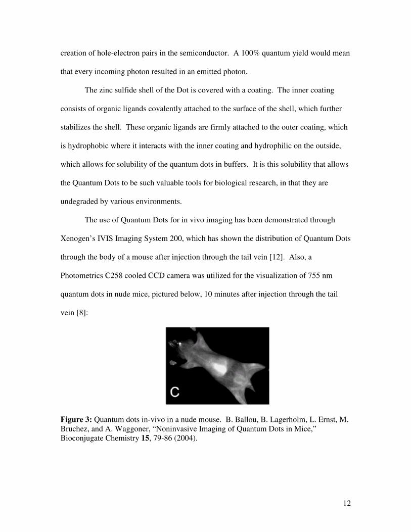
The use of Quantum Dots for in vivo imaging has been demonstrated through
Xenogen’s IVIS Imaging System 200, which has shown the distribution of Quantum Dots
through the body of a mouse after injection through the tail vein [12]. Also, a
Photometrics C258 cooled CCD camera was utilized for the visualization of 755 nm
quantum dots in nude mice, pictured below, 10 minutes after injection through the tail
vein [8]:
Figure 3: Quantum dots in-vivo in a nude mouse. B. Ballou, B. Lagerholm, L. Ernst, M. Bruchez, and A. Waggoner, “Noninvasive Imaging of Quantum Dots in Mice,” Bioconjugate Chemistry 15, 79-86 (2004).
13
2.5 Optics of Quantum Dot Imaging
In order to obtain constant excitation (and thus emission) of light from the
quantum dots, they must be excited by incoming light and their radiation subsequently
detected by the CCD camera. This presents a challenge in the experimental set-up of the
detection system, as one wants the camera to see the light the quantum dots emit but not
the exciting light stimulating the emission. The CCD camera used here is a monochrome
device, as it cannot distinguish between the varying wavelengths of light that register on
its chip. Therefore, one must use a device external to the camera to establish selective
detection of light. The use of interference filters provides a solution to this problem [8].
Optical filters are defined by the part of the spectrum which they pass or exclude
[9]. By selecting the correct interference filter, one can effectively limit the “vision” of a
device such as a camera by preventing light of certain wavelengths from reaching the
detector. Bandpass interference filters allow light of only specific wavelengths to pass
through, and they reflect all other wavelengths of light.
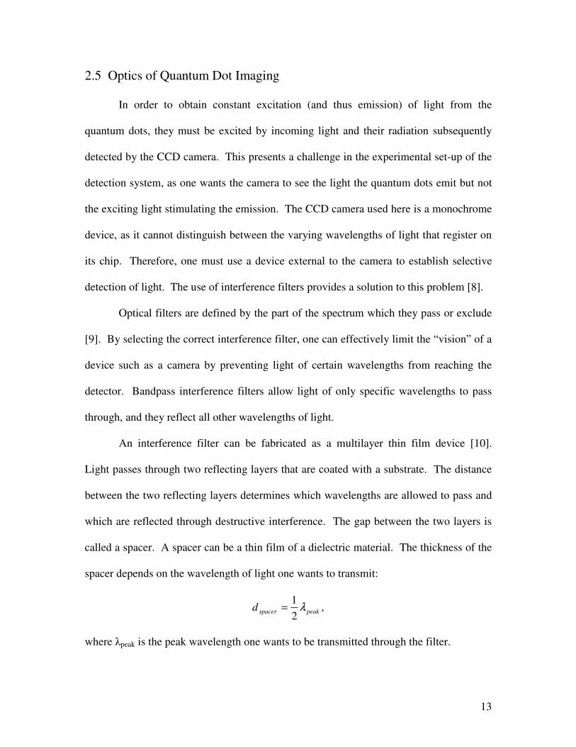
An interference filter can be fabricated as a multilayer thin film device [10].
Light passes through two reflecting layers that are coated with a substrate. The distance
between the two reflecting layers determines which wavelengths are allowed to pass and
which are reflected through destructive interference. The gap between the two layers is
called a spacer. A spacer can be a thin film of a dielectric material. The thickness of the
spacer depends on the wavelength of light one wants to transmit:
,2
1peakspacerd λ=
where λpeak is the peak wavelength one wants to be transmitted through the filter.
14
The two layers on either side of the spacer are composed of several film layers,
each of which has a thickness of ¼ the desired wavelength. The compositions of these
layers alternate between materials of a high and low index of refraction. Typically zinc
sulfide serves as the high index material and cryolite (Na3AlF6) is the low index material.
This series of layers is referred to as a stack. The combination of two stacks and the
spacer comprise a “one cavity” bandpass filter [10].
A one cavity bandpass filter, however, does not provide the sharpest contrast
between wavelengths of light, and thus one may employ multiple cavity bandpass filters
which can serve to fine-tune the filter’s selectivity. Multiple cavity bandpass filters
consist of several one cavity bandpass filters stacked together. Finally, to ensure only the
passage of light of the desired wavelength, a blocking layer is added to the filter, which
utilizes the principles of destructive interference to prevent "shoot through" of light not in
the desired band. The blocking layers and passband layers are covered with a glass
subtrate and sealed in a protective metal case with optical epoxy [10].
Figure 4: A single-cavity bandpass filter
In imaging quantum dots, one seeks to maximize the Stokes shift, which is
defined as the difference in wavelengths between the absorption and emission spectra
spacer
d = ½ λpeak
high index layer (ZnS) d = ¼ λpeak
Low index layer (Na3AlF6) d = ¼ λpeak

15
[10]. With a large Stokes shift, one can be sure to clearly separate the light absorbed by
the quantum dots and the light emitted by the quantum dots through the use of
interference filters.
3 Experiment: Constructing a Cooling System for the Camera
3.1 Peltier Coolers: Experimental Set-up
In a test intended to attempt to draw more heat away from the camera,
supplemental Peltier coolers were purchased. These Peltier coolers, like the ones inside
the ST-6, make use of the electron energy differences in different metals [7].
After connecting a Peltier cooler to a power supply and supplying voltage it was
noticed that the isolation of the heat did not last long, and after several minutes the entire
Peltier cooler began to warm, unable to dissipate all the heat produced. In order to help
conduct some of the heat away from the Peltier coolers, aluminum heat sinks were
designed. The Peltier coolers, hot side connected to the aluminum sticks (Figure 3) were
pressed, cold side down, to the heat radiator at the top of the CCD camera to draw heat
away from the camera. A voltage difference of 3.5 V was applied to the Peltier coolers,
and data were collected examining the heat gain in the electronics starting from -30 °C,
the lowest temperature the camera had thus far attained.

16
Figure 5: The Peltier cooler, connected to a voltage source, laying, hot side down, on an aluminum heat sink, in order to conduct heat away from the Peltier cooler.
3.2 Liquid Nitrogen Circulation: Experimental Set-up
Liquid nitrogen has several properties which make it a viable option for cooling
the CCD. In its gas form, it is both very cold and very “dry,” and thus will deposit
minimal condensation on the camera if it is used in moderation. When considering how
to utilize liquid nitrogen evaporate, one must take into consideration the amount of
cooling the camera can tolerate without condensation, which would harm the electronics,
as evidenced from a previous experiment:
A method of cooling utilizing liquid nitrogen had been tested previously. Two
dewers containing liquid nitrogen were set up directly below the camera, which was
supported by a ring stand and two aluminum sinks in contact with the liquid nitrogen.
Without any temperature regulation by the CCD, the liquid nitrogen cooled the CCD chip
to a low of -102 °C, and the temperature then stabilized at -85 °C. However, frost
collected on both the camera and the aluminum sticks. This resulted in condensation on
and within the camera. The camera was opened up, and allowed to dry out, and no harm
appears to have resulted.
17
However, this raised concerns as to how to safely cool the camera without the
danger of damaging it through condensation. Discussion with Mr. Alan Holmes of Santa
Barbara Instrument Group made it clear that care must be taken not to overcool the
camera in order to avoid the precipitation of excess moisture that could harm the
electronics. Taking that into consideration, the following system utilizing liquid nitrogen
evaporate was designed and tested:
The camera was removed from its original large plywood black box, and a new
box was constructed, using a wall cabinet of approximate dimensions of 68 cm x 33.5 cm
x 27 cm. The box was lined with Styrofoam, a shelf installed in the middle and the
bottom half and door painted flat black to prevent reflection of light. Cracks were sealed
and a frame was built around the inside of the door to prevent light from entering, thus
making the box light-tight. A hole was put in the middle of the shelf so that the larger,
top part of the camera could rest on the shelf and the lens could go through into the
bottom half of the cabinet, where the object being imaged would be placed. The wire that
connected the CCD camera with the central processing unit (CPU) was put through a hole
in the top of the cabinet.
An original test of a method using liquid nitrogen evaporate to cool the camera
consisted of connecting a long foam tube to the top of a liquid nitrogen dewer. Inside the
dewer, a 20 Ω resister was connected to a power supply and approximately 5 V was
applied to the resistor. However, after a few trials and no temperature change on the
inside of the box, it was determined that the liquid nitrogen was not evaporating quickly
enough. The design was altered to the one pictured below:

18
Figure 6: The final set-up the liquid nitrogen evaporate cooling system. The liquid nitrogen boils in the metal can and the cold gas passes through the gray foam tube and into the upper chamber of the cabinet, where the camera is located. The cold vapor moves over the camera, drawing heat away, and then leaves the upper chamber through the venting tube at the top. The liquid nitrogen dewer was replaced by a clean, dry metal can of volume .0123
m3 filled to approximately ¾ of its volume with liquid nitrogen. The liquid nitrogen boils
off at room temperature and the metal can, unlike the liquid nitrogen dewer, exerts
enough pressure on the evaporate so that it is forced through the foam tube.
3.3 Results and Analysis
Our results for each of the methods (no cooling, Peltier coolers, and liquid
nitrogen evaporate) are presented in the graph below. The Peltier coolers provided a
slight improvement, but not enough to practically improve the image quality of the
camera.
The method of circulating liquid nitrogen evaporate using the pressure exerted by
the sealed paint can, however, provided an ideal solution to the problem of cooling the
charge-coupled device camera. The lowest temperature the camera had safely reached

19
was -30 °C, but the liquid nitrogen evaporate brought it down to -50 °C, with no visible
condensation on the camera.
Methods of Cooling the CCD Camera: A
Comparison
-60
-50
-40
-30
-20
-10
0 300 600 900 1200 1500
Time (s)
Tem
per
atu
re
(deg
rees
Cel
siu
s)
No coolingPeltier coolersLiq. NitrogenLinear (Liq. Nitrogen)Linear (Peltier coolers)Linear (No cooling)
Figure 7: Results of Various Methods for Cooling the Camera
4 Experiment: The Camera as a Tool for Biological Research
4.1 Quantum Dots: Experimental Set-up
In designing an experimental set-up for the uses of quantum dots, one must take
into account the optical parameters of such a system. To stimulate emission of the
quantum dots, one utilizes high energy (short wavelength) light. Thus, one selects
quantum dots that emit at a lower energy (longer wavelength) light than the exciting
source.

20
For purposes of this work, QTrackerTM 800 Non-targeted quantum dots were
selected. They emit light at 800 nm, the longest wavelength emission offered, which is in
the near-infrared region of the electromagnetic spectrum. This is well within the CCD
camera’s range of detection, which ranges from approximately 300 nm – 1000 nm. Non-
targeted Quantum Dots are specifically developed to reduce interactions with other
molecules.
Figure 8: vial with 190 µL QTrackerTM 800 Non-targeted quantum dots, and 10 µL “dot” in Petri dish (right) used for test images (200 µL total). Filters were purchased from Edmund Industrial Optics for use in this set-up.
These included an 800 nm bandpass interference filter, a red dichroic filter, a blue
dichroic filter, and a cyan dichroic filter.
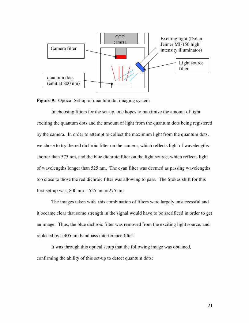
The basic set-up for the quantum dot imaging project is diagrammed below in
Figure 7:
21
Figure 9: Optical Set-up of quantum dot imaging system
In choosing filters for the set-up, one hopes to maximize the amount of light
exciting the quantum dots and the amount of light from the quantum dots being registered
by the camera. In order to attempt to collect the maximum light from the quantum dots,
we chose to try the red dichroic filter on the camera, which reflects light of wavelengths
shorter than 575 nm, and the blue dichroic filter on the light source, which reflects light
of wavelengths longer than 525 nm. The cyan filter was deemed as passing wavelengths
too close to those the red dichroic filter was allowing to pass. The Stokes shift for this
first set-up was: 800 nm – 525 nm = 275 nm
The images taken with this combination of filters were largely unsuccessful and
it became clear that some strength in the signal would have to be sacrificed in order to get
an image. Thus, the blue dichroic filter was removed from the exciting light source, and
replaced by a 405 nm bandpass interference filter.
It was through this optical setup that the following image was obtained,
confirming the ability of this set-up to detect quantum dots:
CCD camera
quantum dots
(emit at 800 nm)
Light source
filter
Camera filter
Exciting light (Dolan-Jenner MI-150 high
intensity illuminator)

22
Figure 10: Image obtained of quantum dots, utilizing the red dichroic filter on the camera and a 405 nm bandpass filter on the exciting light source.
The dot in the middle of the picture in Figure 8 is the 10 µL in the middle of the
Petri dish in Figure 6. The reflection of the Petri dish is the figure encircling the quantum
dot. One can also see a light ring of light around the reflection of the dish, which is
consistent with the edge of the light used to excite the quantum dots. Thus the camera
was detecting some of the exciting light, to a small degree.
In order to improve the image, the red dichroic filter on the camera was replaced
with the 800 nm bandpass filter, and the following image was obtained:
Figure 11: Image obtained of quantum dots, utilizing the 800 nm bandpass filter on the camera and a 405 nm bandpass filter on the exciting light source.
The light from the exciting source has been substantially reduced in this image, as
the Stokes shift is increased to: 800 nm – 405 nm = 395 nm.
23
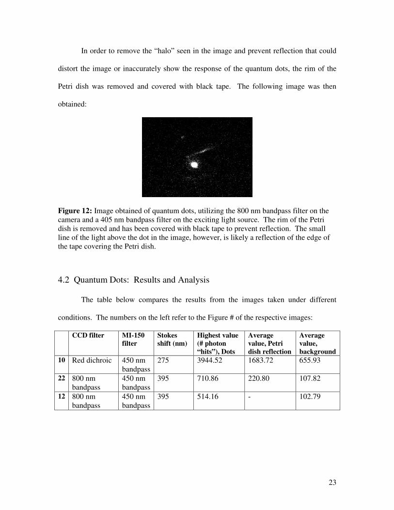
In order to remove the “halo” seen in the image and prevent reflection that could
distort the image or inaccurately show the response of the quantum dots, the rim of the
Petri dish was removed and covered with black tape. The following image was then
obtained:
Figure 12: Image obtained of quantum dots, utilizing the 800 nm bandpass filter on the camera and a 405 nm bandpass filter on the exciting light source. The rim of the Petri dish is removed and has been covered with black tape to prevent reflection. The small line of the light above the dot in the image, however, is likely a reflection of the edge of the tape covering the Petri dish.
4.2 Quantum Dots: Results and Analysis
The table below compares the results from the images taken under different
conditions. The numbers on the left refer to the Figure # of the respective images:
CCD filter MI-150
filter
Stokes
shift (nm)
Highest value
(# photon
“hits”), Dots
Average
value, Petri
dish reflection
Average
value,
background
10 Red dichroic 450 nm bandpass
275 3944.52 1683.72 655.93
22 800 nm bandpass
450 nm bandpass
395 710.86 220.80 107.82
12 800 nm bandpass
450 nm bandpass
395 514.16 - 102.79

24
The average number of photon hits from a certain part of the image was determined using
CCDOps, the image analysis program that accompanies the ST-6. In performing the
analysis, the highest number from each of the regions was utilized.
One can see that in Image 1, a great deal of the light that appeared to be coming
from the quantum dot was actually due to reflection from the Petri dish and light from the
source that was reaching the camera. Subsequent adjustments to the filters and reduction
of the reflection-causing Petri dish allowed one to detect only the actual light being
emitted from the quantum dot.
An important part of in vivo biological imaging is dealing with the optical
properties of animal tissue. In order to get a general idea of how well this system images
quantum dots through tissue, clear microscope slides had been dipped in paraffin and
allowed to dry. Paraffin has optical properties similar to that of animal tissue of a similar
thickness. The slides were dipped in hot paraffin various times, so that each had a
different thickness. Images were taken using the following set-up:
Figure 13: A diagram of the set-up used to determine the amount of light from the dots that would pass through various thicknesses of paraffin on a microscope slide. The distance from the dots to the paraffin slide is 6.5 cm. Of note: The exciting light (blue) does not pass through the paraffin slide. Only the emitted (red) light passes through the slide.
Paraffin slide Quantum dots

25
2.00 second exposures were taken at 0 °C. The images were analyzed using
CCDOps, and average photon counts from the area of the slide were taken. Below is a
sample image:
Figure 14: A sample image from the trial with one full slide of paraffin. Though there is considerable diffusion from behind the paraffin, one can clearly distinguish the light coming from the dot.
The results were as follows:
Figure 15: Thickness of Slide vs. Average Photon Counts. The first point, at a slide thickness of 0, was taken with no slide between the dot and the camera. The second point, at a slide thickness of 0.08 cm, represents the thickness of only the glass slide, with no paraffin on it. The third data point represents the first slide actually dipped in paraffin.
Total Thickness of Slide
vs. Average Photon Counts
0
100
200
300
400
500
600
0 0.1 0.2 0.3 0.4 0.5 Thickness of slide (cm)
Avg. Photon Counts

26
Thus, “Total Thickness of Slide” refers to the total amount of material between the dot and the camera, 0.08 cm of that being the blank slide and the rest comprised of paraffin.
One can see that there is a minor drop in visibility when a glass slide is placed
between the dot and the camera. There is a significant drop when the first paraffin slide
is used, and as shown in Figure 12, there is considerable diffusion through the material.
Subsequent images show that the thickness of the paraffin, up to nearly 0.5 cm, does not
make a major difference in visibility. Background was generally at around 80 photon
counts. One can expect even more contrast with background when the CCD camera is
cooled using the liquid nitrogen system described earlier.
Conclusion
The goal of this project was twofold: first, to find an economical but successful
method of cooling the camera; and second, to show that this camera can be used to
conduct biological research.
The first goal was met: liquid nitrogen is an inexpensive commodity, and the
camera attained and held a temperature of -50 °C. Since no condensation was apparent
on the camera after 25 minutes, at which point the metal can of liquid nitrogen ran out,
one could presumably refill the can and continue to cool the camera for longer using the
apparatus.
The camera’s ability to see quantum dots both in the open and behind a barrier
simulating animal tissue shows the instrument’s promise for the future. Quantum dots
can be purchased as a part of a conjugation kit, in which they bind to specific substances
in an animal’s body. This can provide valuable information contributing to the study of

27
tumors and the spread of infections in animals. The ultimate realization of this second
goal will be to eventually see the quantum dots in vivo in an animal.
Bibliography
[1.] R.W. Ditchburn, “Light,” (Academic Press, Inc., London, 1976).
[2.] M.J. Howes and D.V. Morgan, “Charge-coupled Devices and Systems,” (John Wiley
& Sons, Inc., New York, 1979).
[3.] K.P. Francis, D. Joh, C. Kawahara-Bellinger, M.J. Hawkinson, T.F. Purchio, P.R.
Contag, “Monitoring Bioluminescent Staphylococcus auereus Infections in Living
Mice Using a Novel luxABCDE Construct,” Infection and Immunity 68, No. 6, 3594
(2000).
[4.] K.J. Smith, “Visible Light Imaging of Small Animals,” College of William and
Mary, Williamsburg, 2003.
[5.] P. Sprawls, “Physical Principles of Medical Imaging,” (Medical Physics Publishing,
Madison, 1993).
[6.] R. Berry, “Choosing and Using a CCD Camera,” (Willmann-Bell, Inc., Richmond,
1993).

28
[7.] R. Berry, V. Kanto, and J. Munger, “The CCD Camera Cookbook,” (Willmann-Bell,
Inc., 1994).
[8.] B. Ballou, B. Lagerholm, L. Ernst, M. Bruchez, and A. Waggoner, “Noninvasive
Imaging of Quantum Dots in Mice,” Bioconjugate Chemistry 15, 79-86 (2004).
[9.] Edmund Industrial Optics
http://www.edmundoptics.com/techSupport
[10.] C & L Instruments, Inc.
http://www.fluorescence.com/tutorial/int-filt.htm
[11.] Quantum Dot Corporation
http://www.qdots.com
[12.] Quantum Dot Corporation, “Quantum Dot Vision,” November, 2004.
[13.] Real World Technologies
http://www.realworldtech.com/page.cfm?ArticleID=RWT050802020022