Embed Size (px)
Citation preview

A Tutorial
On
Advanced Analysis
For
Cadence Spectre
Prepared By:
Rishi Todani
Web: http://www.32mosfets.com
With Guidance, Encouragement and Blessing FromDr. Ashis Kumar Mal
Associate Professor, ECE Department,NIT Durgapur
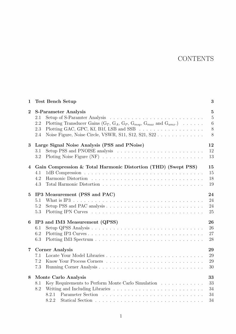
CONTENTS
1 Test Bench Setup 3
2 S-Parameter Analysis 52.1 Setup of S-Paramter Analysis . . . . . . . . . . . . . . . . . . . . . . . . . . 52.2 Plotting Transducer Gains (GT , GA, GP , Gmsg, Gmax and Gumx.) . . . . . . 62.3 Plotting GAC, GPC, Kf, B1f, LSB and SSB . . . . . . . . . . . . . . . . . . 82.4 Noise Figure, Noise Circle, VSWR, S11, S12, S21, S22 . . . . . . . . . . . . . 8
3 Large Signal Noise Analysis (PSS and PNoise) 123.1 Setup PSS and PNOISE analysis . . . . . . . . . . . . . . . . . . . . . . . . 123.2 Ploting Noise Figure (NF) . . . . . . . . . . . . . . . . . . . . . . . . . . . . 13
4 Gain Compression & Total Harmonic Distortion (THD) (Swept PSS) 154.1 1dB Compression . . . . . . . . . . . . . . . . . . . . . . . . . . . . . . . . . 154.2 Harmonic Distortion . . . . . . . . . . . . . . . . . . . . . . . . . . . . . . . 184.3 Total Harmonic Distortion . . . . . . . . . . . . . . . . . . . . . . . . . . . . 19
5 IP3 Measurement (PSS and PAC) 245.1 What is IP3 . . . . . . . . . . . . . . . . . . . . . . . . . . . . . . . . . . . . 245.2 Setup PSS and PAC analysis . . . . . . . . . . . . . . . . . . . . . . . . . . . 245.3 Plotting IPN Curves . . . . . . . . . . . . . . . . . . . . . . . . . . . . . . . 25
6 IP3 and IM3 Measurement (QPSS) 266.1 Setup QPSS Analysis . . . . . . . . . . . . . . . . . . . . . . . . . . . . . . . 266.2 Plotting IP3 Curves . . . . . . . . . . . . . . . . . . . . . . . . . . . . . . . . 276.3 Plotting IM3 Spectrum . . . . . . . . . . . . . . . . . . . . . . . . . . . . . . 28
7 Corner Analysis 297.1 Locate Your Model Libraries . . . . . . . . . . . . . . . . . . . . . . . . . . . 297.2 Know Your Process Corners . . . . . . . . . . . . . . . . . . . . . . . . . . . 297.3 Running Corner Analysis . . . . . . . . . . . . . . . . . . . . . . . . . . . . . 30
8 Monte Carlo Analysis 338.1 Key Requirements to Perform Monte Carlo Simulation . . . . . . . . . . . . 338.2 Writing and Including Libraries . . . . . . . . . . . . . . . . . . . . . . . . . 34
8.2.1 Parameter Section . . . . . . . . . . . . . . . . . . . . . . . . . . . . 348.2.2 Statical Section . . . . . . . . . . . . . . . . . . . . . . . . . . . . . . 34
1

CONTENTS 2
8.2.3 Model Section . . . . . . . . . . . . . . . . . . . . . . . . . . . . . . . 358.3 Running Monte Carlo Simulation . . . . . . . . . . . . . . . . . . . . . . . . 358.4 Additional Information . . . . . . . . . . . . . . . . . . . . . . . . . . . . . . 36
8.4.1 Specifying Distributions . . . . . . . . . . . . . . . . . . . . . . . . . 368.4.2 Correlation Statements . . . . . . . . . . . . . . . . . . . . . . . . . . 38
8.5 Sample Monte Carlo Library File . . . . . . . . . . . . . . . . . . . . . . . . 39
Prepared By: Rishi Todani [email protected] http://www.32mosfets.com
CHAPTER
ONE
TEST BENCH SETUP
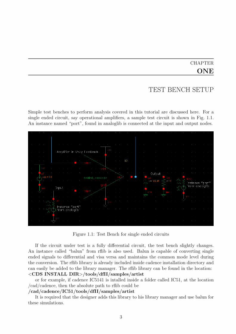
Simple test benches to perform analysis covered in this tutorial are discussed here. For asingle ended circuit, say operational amplifiers, a sample test circuit is shown in Fig. 1.1.An instance named “port”, found in analoglib is connected at the input and output nodes.
Figure 1.1: Test Bench for single ended circuits
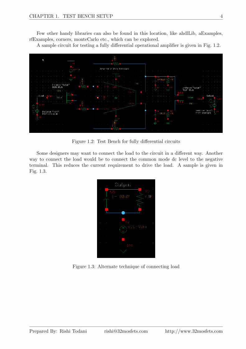
If the circuit under test is a fully differential circuit, the test bench slightly changes.An instance called “balun” from rflib is also used. Balun is capable of converting singleended signals to differential and visa versa and maintains the common mode level duringthe conversion. The rflib library is already included inside cadence installation directory andcan easily be added to the library manager. The rflib library can be found in the location:<CDS INSTALL DIR>/tools/dfII/samples/artist
or for example, if cadence IC5141 is intalled inside a folder called IC51, at the location/cad/cadence, then the absolute path to rflib could be/cad/cadence/IC51/tools/dfII/samples/artist
It is required that the designer adds this library to his library manager and use balun forthese simulations.
3
CHAPTER 1. TEST BENCH SETUP 4
Few other handy libraries can also be found in this location, like ahdlLib, aExamples,rfExamples, corners, monteCarlo etc., which can be explored.
A sample circuit for testing a fully differential operational amplifier is given in Fig. 1.2.
Figure 1.2: Test Bench for fully differential circuits
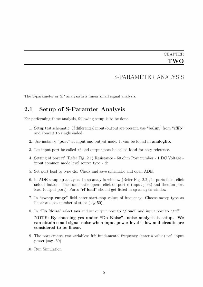
Some designers may want to connect the load to the circuit in a different way. Anotherway to connect the load would be to connect the common mode dc level to the negativeterminal. This reduces the current requirement to drive the load. A sample is given inFig. 1.3.
Figure 1.3: Alternate technique of connecting load
Prepared By: Rishi Todani [email protected] http://www.32mosfets.com
CHAPTER
TWO
S-PARAMETER ANALYSIS
The S-parameter or SP analysis is a linear small signal analysis.
2.1 Setup of S-Paramter Analysis
For performing these analysis, following setup is to be done.
1. Setup test schematic. If differential input/output are present, use “balun” from “rflib”and convert to single ended.
2. Use instance “port” at input and output node. It can be found in analoglib.
3. Let input port be called rf and output port be called load for easy reference.
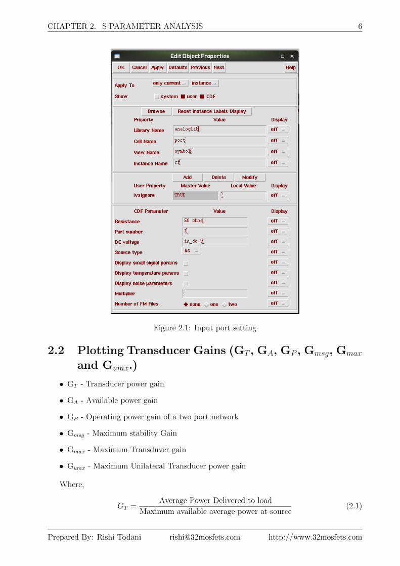
4. Setting of port rf (Refer Fig. 2.1) Resistance - 50 ohm Port number - 1 DC Voltage -input common mode level source type - dc
5. Set port load to type dc. Check and save schematic and open ADE.
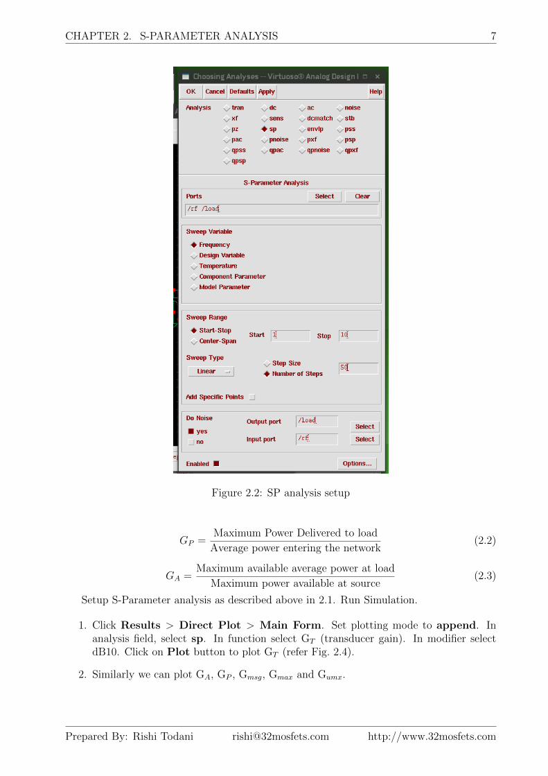
6. in ADE setup sp analysis. In sp analysis window (Refer Fig. 2.2), in ports field, clickselect button. Then schematic opens, click on port rf (input port) and then on portload (output port). Ports “rf load” should get listed in sp analysis window.
7. In “sweep range” field enter start-stop values of frequency. Choose sweep type aslinear and set number of steps (say 50).
8. In “Do Noise” select yes and set output port to “/load” and input port to “/rf”
NOTE: By choosing yes under “Do Noise”, noise analysis is setup. Wecan obtain small signal noise when input power level is low and circuits areconsidered to be linear.
9. The port creates two variables: frf: fundamental frequency (enter a value) prf: inputpower (say -50)
10. Run Simulation
5
CHAPTER 2. S-PARAMETER ANALYSIS 6
Figure 2.1: Input port setting
2.2 Plotting Transducer Gains (GT , GA, GP , Gmsg, Gmax
and Gumx.)
• GT - Transducer power gain
• GA - Available power gain
• GP - Operating power gain of a two port network
• Gmsg - Maximum stability Gain
• Gmax - Maximum Transduver gain
• Gumx - Maximum Unilateral Transducer power gain
Where,
GT =Average Power Delivered to load
Maximum available average power at source(2.1)
Prepared By: Rishi Todani [email protected] http://www.32mosfets.com
CHAPTER 2. S-PARAMETER ANALYSIS 7
Figure 2.2: SP analysis setup
GP =Maximum Power Delivered to load
Average power entering the network(2.2)
GA =Maximum available average power at load
Maximum power available at source(2.3)
Setup S-Parameter analysis as described above in 2.1. Run Simulation.
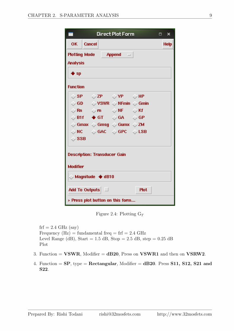
1. Click Results > Direct Plot > Main Form. Set plotting mode to append. Inanalysis field, select sp. In function select GT (transducer gain). In modifier selectdB10. Click on Plot button to plot GT (refer Fig. 2.4).
2. Similarly we can plot GA, GP , Gmsg, Gmax and Gumx.
Prepared By: Rishi Todani [email protected] http://www.32mosfets.com
CHAPTER 2. S-PARAMETER ANALYSIS 8
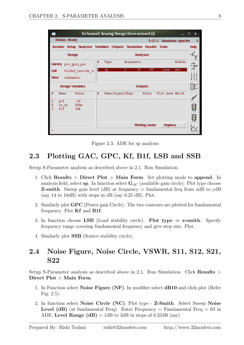
Figure 2.3: ADE for sp analysis
2.3 Plotting GAC, GPC, Kf, B1f, LSB and SSB
Setup S-Parameter analysis as described above in 2.1. Run Simulation.
1. Click Results > Direct Plot > Main Form. Set plotting mode to append. Inanalysis field, select sp. In function select GAC (available gain circle). Plot type chooseZ-smith. Sweep gain level (dB) at frequency = fundamental freq from xdB to ydB(say 14 to 18dB) with steps in dB (say 0.25 dB). Plot.
2. Similarly plot GPC (Power gain Circle). The two contours are plotted for fundamentalfrequency. Plot Kf and B1f.
3. In function choose LSB (Load stability circle). Plot type = z-smith. Specifyfrequency range covering fundamental frequency and give step size. Plot.
4. Similarly plot SSB (Source stability circle).
2.4 Noise Figure, Noise Circle, VSWR, S11, S12, S21,
S22
Setup S-Parameter analysis as described above in 2.1. Run Simulation. Click Results >Direct Plot > Main Form.
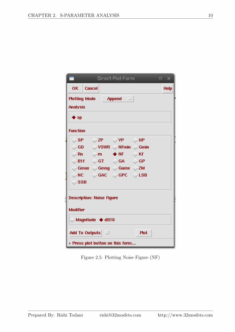
1. In Function select Noise Figure (NF). In modifier select dB10 and click plot (ReferFig. 2.5).
2. In function select Noise Circle (NC). Plot type - Z-Smith. Select Sweep NoiseLevel (dB) (at fundamental Freq). Enter Frequency = Fundamental Freq = frf inADE. Level Range (dB) = 1dB to 3dB in steps of 0.25dB (say)
Prepared By: Rishi Todani [email protected] http://www.32mosfets.com
CHAPTER 2. S-PARAMETER ANALYSIS 9
Figure 2.4: Plotting GT
frf = 2.4 GHz (say)Frequency (Hz) = fundamental freq = frf = 2.4 GHzLevel Range (dB), Start = 1.5 dB, Stop = 2.5 dB, step = 0.25 dBPlot
3. Function = VSWR, Modifier = dB20, Press on VSWR1 and then on VSRW2.
4. Function = SP, type = Rectangular, Modifier = dB20. Press S11, S12, S21 andS22.
Prepared By: Rishi Todani [email protected] http://www.32mosfets.com
CHAPTER 2. S-PARAMETER ANALYSIS 10
Figure 2.5: Plotting Noise Figure (NF)
Prepared By: Rishi Todani [email protected] http://www.32mosfets.com
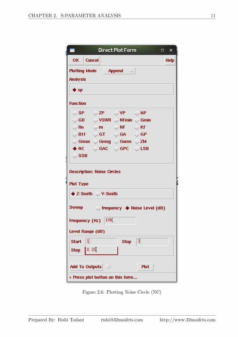
CHAPTER 2. S-PARAMETER ANALYSIS 11
Figure 2.6: Plotting Noise Circle (NC)
Prepared By: Rishi Todani [email protected] http://www.32mosfets.com
CHAPTER
THREE
LARGE SIGNAL NOISE ANALYSIS (PSS AND PNOISE)
Use PSS and PNoise analysis for large signal and non-linear noise analysis, when the circuitsare linearised around the periodic steady state operating point.
Use Noise and SP analysis for small signal and linear noise analysis when the circuits arelinearized around DC operating point.
As input power increases, the circuit becomes non-linear, the harminocs are generatedand the noise spectrum is folded. Therefore, we should use PSS and PNoise analysis.
When Input power level remains low, the Noise Figure calculated from PNoise, PSP,Noise and SP analysis should all match.
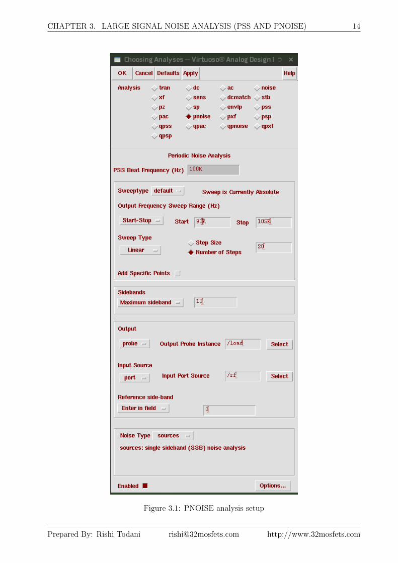
3.1 Setup PSS and PNOISE analysis
Add “port” to input and output of schematic and do the following settings
1. In schematic, select input port “rf”Port no. = 1DC volt = 0.9 or Vdd/2 or VCMsource type = sinefrequency name = rffreq 1 = frf (this is the fundamental frequency)amplitude 1 (dBm) = prf
2. In ADE, copy variables from schematic and enter values of frf and prf.frf = 100K (say)prf = -40
3. Setup PSS analysis in ADE.Select Auto calculate for beat frequency. It automatically takes it as frf.Set number of harmonics to 10. This allows us to look at in the frequency domainresults with 10 harmonics of beat frequency.Select Moderate accuracy.
12
CHAPTER 3. LARGE SIGNAL NOISE ANALYSIS (PSS AND PNOISE) 13
4. In ADE, under analysis, choose PNOISE. Refer Fig. 3.1Specify noise source and number of side bands. The larger the number of side bands,the more accurate the results.Set reference sideband as 0 if your circuit has no frequency conversion from input tooutput (amplifier).Sweep type - defaultGive a start - stop range covering the fundamental frequency (say 95K to 105K)Specify number of steps = 20 (say)Maximum sidebands = 10Output source - Probe /load (output port)Input source - Probe /rf (input port)Reference sideband = 0 (for amplifiers)Click OK and run Simulation
3.2 Ploting Noise Figure (NF)
To plot Noise Figure (NF), open Direct Plot > Main Form.Select Analysis - PNOISE50
Prepared By: Rishi Todani [email protected] http://www.32mosfets.com
CHAPTER 3. LARGE SIGNAL NOISE ANALYSIS (PSS AND PNOISE) 14
Figure 3.1: PNOISE analysis setup
Prepared By: Rishi Todani [email protected] http://www.32mosfets.com
CHAPTER
FOUR
GAIN COMPRESSION & TOTAL HARMONIC DISTORTION
(THD) (SWEPT PSS)
Setup the test bench by connecting port at input and output. Let input port be called rfand output be called load.
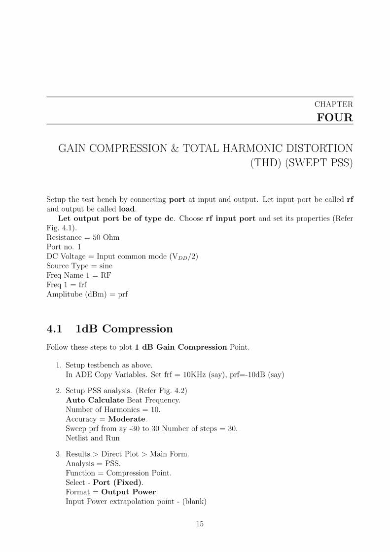
Let output port be of type dc. Choose rf input port and set its properties (ReferFig. 4.1).Resistance = 50 OhmPort no. 1DC Voltage = Input common mode (VDD/2)Source Type = sineFreq Name 1 = RFFreq 1 = frfAmplitube (dBm) = prf
4.1 1dB Compression
Follow these steps to plot 1 dB Gain Compression Point.
1. Setup testbench as above.In ADE Copy Variables. Set frf = 10KHz (say), prf=-10dB (say)
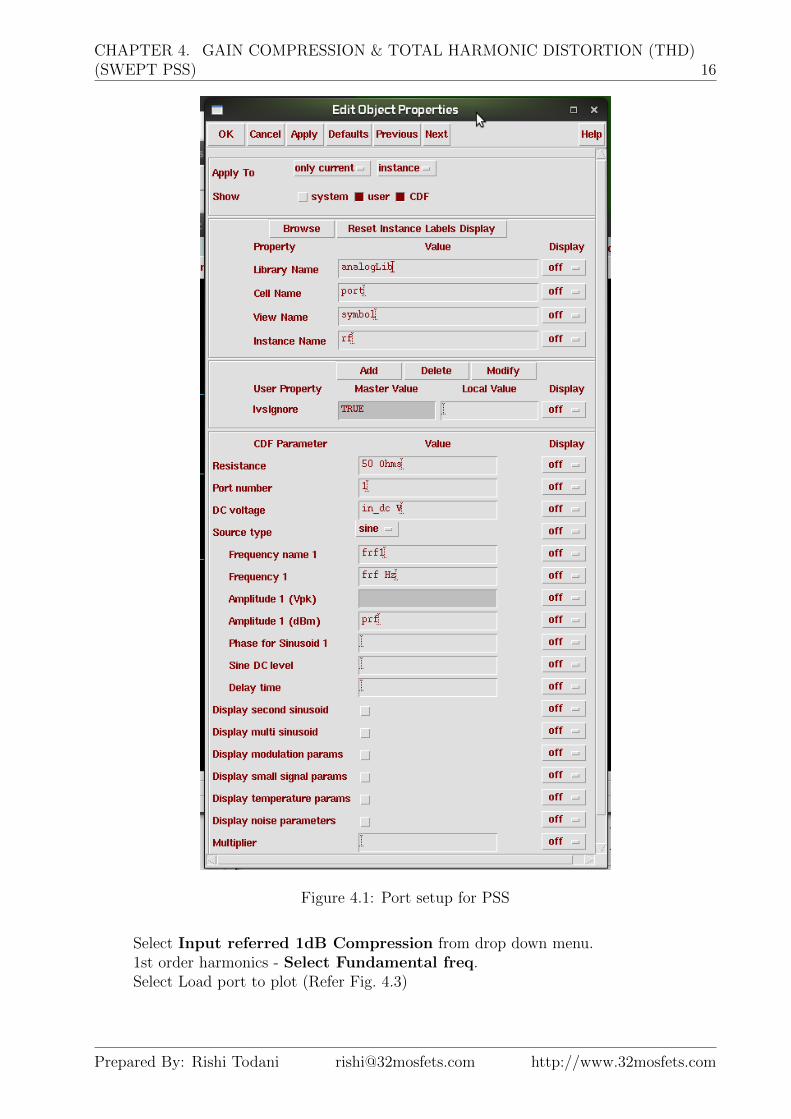
2. Setup PSS analysis. (Refer Fig. 4.2)Auto Calculate Beat Frequency.Number of Harmonics = 10.Accuracy = Moderate.Sweep prf from ay -30 to 30 Number of steps = 30.Netlist and Run
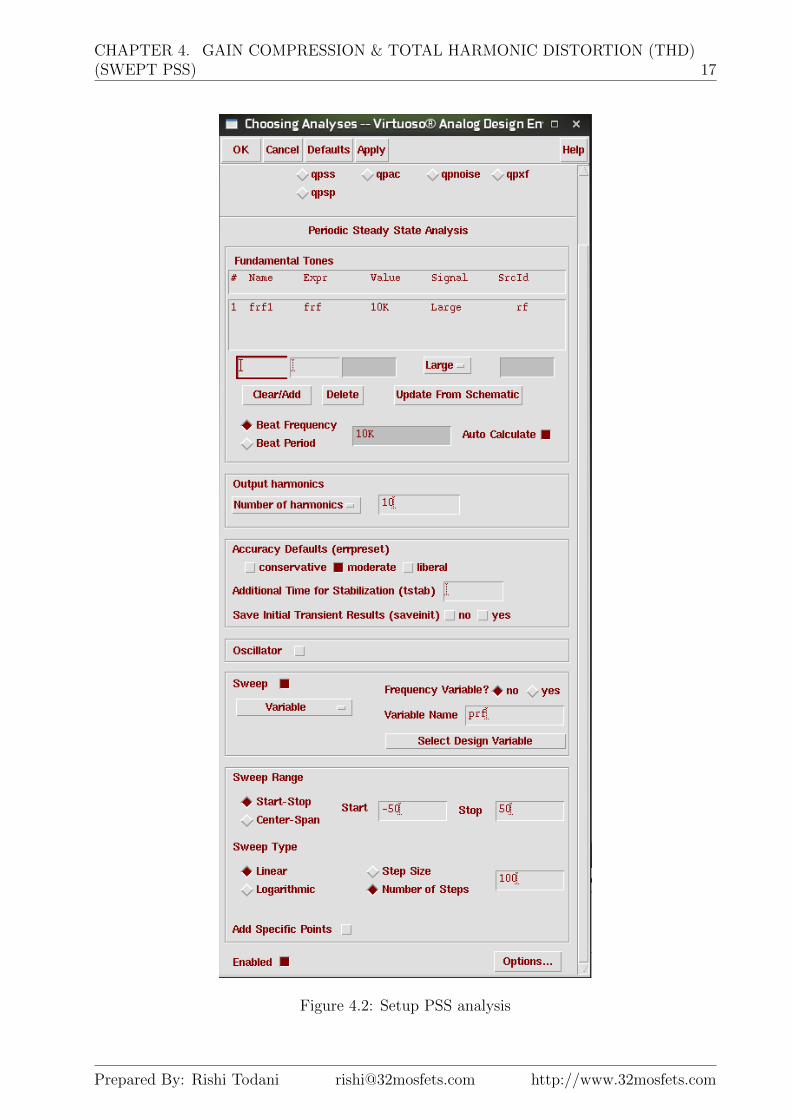
3. Results > Direct Plot > Main Form.Analysis = PSS.Function = Compression Point.Select - Port (Fixed).Format = Output Power.Input Power extrapolation point - (blank)
15
CHAPTER 4. GAIN COMPRESSION & TOTAL HARMONIC DISTORTION (THD)(SWEPT PSS) 16
Figure 4.1: Port setup for PSS
Select Input referred 1dB Compression from drop down menu.1st order harmonics - Select Fundamental freq.Select Load port to plot (Refer Fig. 4.3)
Prepared By: Rishi Todani [email protected] http://www.32mosfets.com
CHAPTER 4. GAIN COMPRESSION & TOTAL HARMONIC DISTORTION (THD)(SWEPT PSS) 17
Figure 4.2: Setup PSS analysis
Prepared By: Rishi Todani [email protected] http://www.32mosfets.com
CHAPTER 4. GAIN COMPRESSION & TOTAL HARMONIC DISTORTION (THD)(SWEPT PSS) 18
Figure 4.3: 1dB compression output
NOTE: 1 dB compression point is the point where the two curves on thegraph intersect. The power axis (x axis) given the input power at which theoutput power reduces by 1 dB
4.2 Harmonic Distortion
Harmonic distortion can be observed by plotting the spectrum of any node voltage. Harmonicdistortion is characterised as the ratio of the power of the fundamental signal divided by thesum of the power at the harmonics.
To plot harmonic distortion,
1. Setup testbench as above. In ADE Copy Variables. Set frf = 10KHz (say), prf=-10dB(say)
2. Setup PSS analysis.Auto Calculate Beat Frequency.Number of Harmonics = 10.Accuracy = Moderate.Sweep prf from ay -30 to 30 with number of steps = 10.Netlist and Run
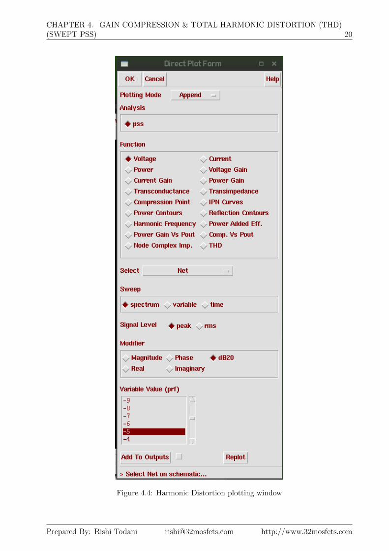
3. Results > Direct Plot > Main Form. (Refer Fig. 4.4)Analysis = PSS.
Prepared By: Rishi Todani [email protected] http://www.32mosfets.com

CHAPTER 4. GAIN COMPRESSION & TOTAL HARMONIC DISTORTION (THD)(SWEPT PSS) 19
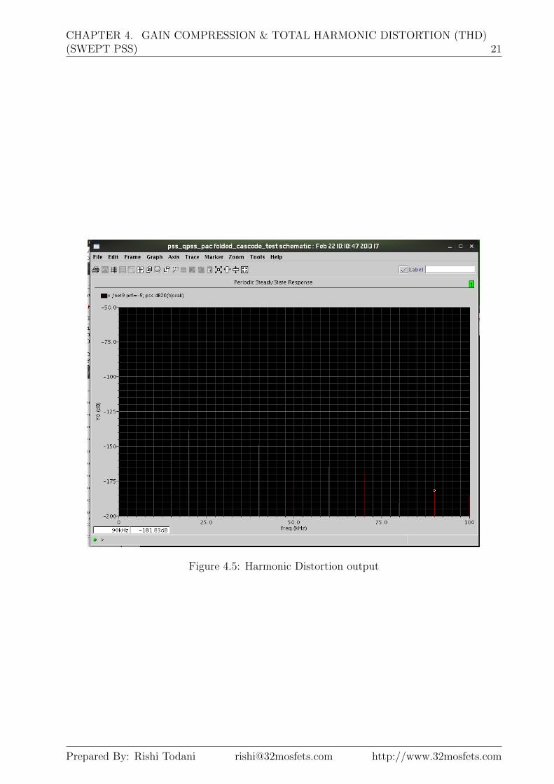
Function = Voltage.Select “net” from drop down menusweep = spectrumSignal level = peakmodifier = dB20Variable value = select power at fundamental freqSelect output Net on schematic to plot (Refer Fig. 4.5)
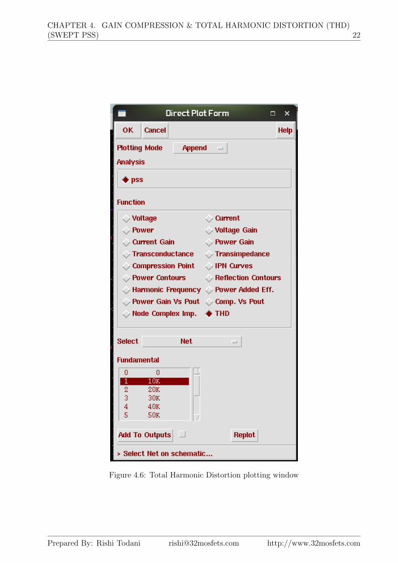
4.3 Total Harmonic Distortion
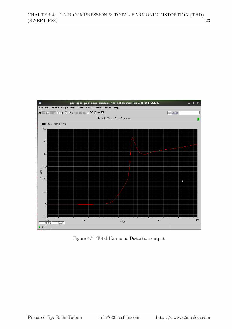
Perform PSS analysis just like Harmonic distortion (Refer Fig. 4.6).In Direct Plot > Main Form, select THD as the function.Choose Fundamental frequency from the frequency sweep list.Click on Output net to plot THD.Plot of percentage THD over input power appears (Refer Fig. 4.5).
Prepared By: Rishi Todani [email protected] http://www.32mosfets.com
CHAPTER 4. GAIN COMPRESSION & TOTAL HARMONIC DISTORTION (THD)(SWEPT PSS) 20
Figure 4.4: Harmonic Distortion plotting window
Prepared By: Rishi Todani [email protected] http://www.32mosfets.com
CHAPTER 4. GAIN COMPRESSION & TOTAL HARMONIC DISTORTION (THD)(SWEPT PSS) 21
Figure 4.5: Harmonic Distortion output
Prepared By: Rishi Todani [email protected] http://www.32mosfets.com
CHAPTER 4. GAIN COMPRESSION & TOTAL HARMONIC DISTORTION (THD)(SWEPT PSS) 22
Figure 4.6: Total Harmonic Distortion plotting window
Prepared By: Rishi Todani [email protected] http://www.32mosfets.com
CHAPTER 4. GAIN COMPRESSION & TOTAL HARMONIC DISTORTION (THD)(SWEPT PSS) 23
Figure 4.7: Total Harmonic Distortion output
Prepared By: Rishi Todani [email protected] http://www.32mosfets.com
CHAPTER
FIVE
IP3 MEASUREMENT (PSS AND PAC)
5.1 What is IP3
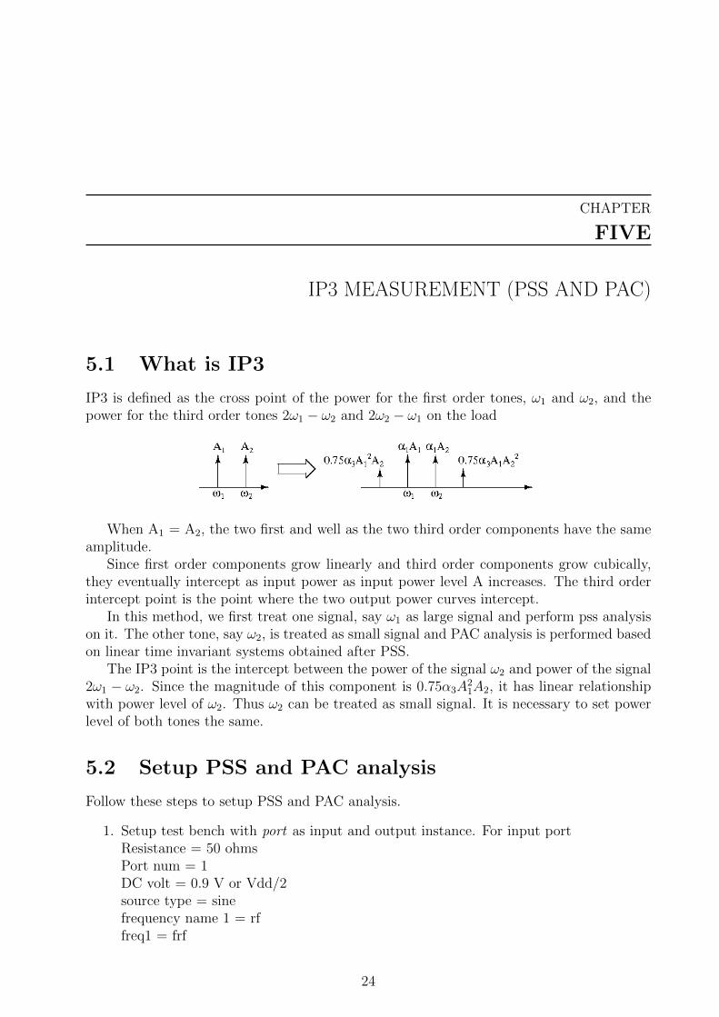
IP3 is defined as the cross point of the power for the first order tones, ω1 and ω2, and thepower for the third order tones 2ω1 − ω2 and 2ω2 − ω1 on the load
When A1 = A2, the two first and well as the two third order components have the sameamplitude.
Since first order components grow linearly and third order components grow cubically,they eventually intercept as input power as input power level A increases. The third orderintercept point is the point where the two output power curves intercept.
In this method, we first treat one signal, say ω1 as large signal and perform pss analysison it. The other tone, say ω2, is treated as small signal and PAC analysis is performed basedon linear time invariant systems obtained after PSS.
The IP3 point is the intercept between the power of the signal ω2 and power of the signal2ω1 − ω2. Since the magnitude of this component is 0.75α3A
21A2, it has linear relationship
with power level of ω2. Thus ω2 can be treated as small signal. It is necessary to set powerlevel of both tones the same.
5.2 Setup PSS and PAC analysis
Follow these steps to setup PSS and PAC analysis.
1. Setup test bench with port as input and output instance. For input portResistance = 50 ohmsPort num = 1DC volt = 0.9 V or Vdd/2source type = sinefrequency name 1 = rffreq1 = frf
24

CHAPTER 5. IP3 MEASUREMENT (PSS AND PAC) 25
Amplitude 1 (dBm) = prf
Select “Display small signal parameters”pac magnitude (dBm) = prf
2. Start ADE and copy variables from schematic. Enter value of frf and prf. frf is ω1
which is the fundamental frequency. Enter prf in negative range say -50 (typically).
3. Setup pss analysis as discussed in earlier chapters. Auto calculate beat frequency(equal to value of frf put in ADE). This is ω1.Set accuracy to moderate.Activate sweep. Sweep power prf from say -50 to -5 dBm in say 20 steps.click OK.
4. Setup PAC analysis.Enter input frequency sweet range. Choose single point and give value of ω2.ω2 should be very slightly larger than ω1 so that 2ω1 − ω2 is nearly ω1.Maximum sideband = 2 (for 3rd order)
5. Simulate. Results > Direct Plot > Main Form.
5.3 Plotting IPN Curves
Select the following under Direct Plot > Main form.Analysis = PACFunction = IPN CurvesDrop down menu Select - Port (Fixed R(port))Circuit Input Power - Variable Sweep (“prf”)Input power extrapolation point (dBm) = -40Select “Input referred IP3” in drop down menuUnder 3rd order harmonic, select the frequency which is equal to 2ω1 − ω2. i.e. If 10K wasentered as frf and 10.025K as the frequency in pac, then 3rd order harmonic becomes 9.975K.Under First order harmonic select the frequency equal to value of ω2 or 10.025K in this case.Click on output port to plot the input referred IP3 in dBm.
Prepared By: Rishi Todani [email protected] http://www.32mosfets.com
CHAPTER
SIX
IP3 AND IM3 MEASUREMENT (QPSS)
This method treats both the tones ω1 and ω2 as large signal and performs QPSS analysis.Both the methods, PSS with PAC and QPSS, are equivalent because of linear dependence
of output components magnitude 2ω1 − ω2 on the input component magnitude ω2.However, for IP3, recommended method is PSS with PAC analysis because it is more
efficient than QPSS.
6.1 Setup QPSS Analysis
Follow the given steps to setup QPSS analysis to plot IP3 and IM3.
1. Setup test bench with port as input and output instance. For input portResistance = 50 ohmsPort num = 1DC volt = 0.9 V or Vdd/2source type = sinefrequency name 1 = rffreq1 = frfAmplitude 1 (dBm) = prffrequency name 2 = rf2freq2 = frf + df (fd is a small delta f)amplitude 2 (dBm) = prf
2. in ADE, copy variable from schematic and set values.prf = -50 (say)frf = 100K (say)df = 0.2k (say)
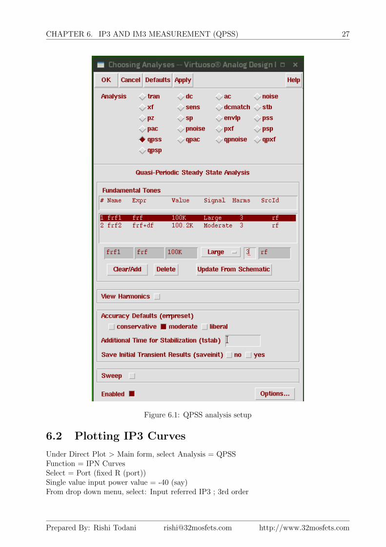
3. Setup QPSS analysis. Refer Fig. 6.1Set frf1 to large signal and frf2 to moderate, since Only one large signal isallowed in QPSSSet accuracy to Moderate.
4. Simulate and choose Direct Plot.
26
CHAPTER 6. IP3 AND IM3 MEASUREMENT (QPSS) 27
Figure 6.1: QPSS analysis setup
6.2 Plotting IP3 Curves
Under Direct Plot > Main form, select Analysis = QPSSFunction = IPN CurvesSelect = Port (fixed R (port))Single value input power value = -40 (say)From drop down menu, select: Input referred IP3 ; 3rd order
Prepared By: Rishi Todani [email protected] http://www.32mosfets.com

CHAPTER 6. IP3 AND IM3 MEASUREMENT (QPSS) 28
In 3rd order harmonic we need to select 2ω1 − ω2
i.e. 2rf1 - rf2In this example = 2x100K - 100.2K = 99.8K
In first order harmonic we select ω2, i.e. 100.2K.
Click on output port to plot IP3 curves
6.3 Plotting IM3 Spectrum
The analysis and simulation required for IM3 is same as IP3 using QPSS analysis. Performthe above same analysis and select the following in Direct Plot > Main form option.Analysis = QPSSFunction = PowerSelect = Port (fixed R (port))Sweep = SpectrumModifier = dB10 or dBmClick on output port to plot
The plot gives the IM3 power plots for the circuit.
Prepared By: Rishi Todani [email protected] http://www.32mosfets.com
CHAPTER
SEVEN
CORNER ANALYSIS
Corner Analysis can be performed using the Analog Corner Analysis tool inside AnalogDesign Environment. Corner analysis is capable of checking the circuit performance at allthe process corners with control over temperature and any other variable at the same time.Running Corner analysis successfully requires some knowledge about the model library filesof the technology under use. The designer must know the path where the model files arestored and also the corners provided by the foundry. The corners can be found by readingthe library files. They are typically marked by sections in the model library file.
7.1 Locate Your Model Libraries
The technology files are typically saved in a folder named designkits in the cadence installa-tion directory. In a typical UNIX system, designkit foler can be found in \cad\cadence\designkits.Inside this directory, more folders can be found corresponding to available technologies. In-side each of the technology folder, a directory named Models can be found. Inside this,model libraries for Spectre and HSPICE can be found in different folders. Spectre modelfiles are typically suffixed with extention .scs. Thus a sample path to model libraries maybe as\<cadence install dir>\designkits\<technology dir>\Models\Spectre\
or\cad\cadence\designkits\UMC180\Models\Spectre\
In this path, *.scs files can be found which contains the device parameters included inthe technology. Find out of the file which contains the MOSFET parameters. In UMC180,the MOSFET parameters are given in file MM180 REG18 V124.mdl.scs and .lib.scs. MDLfile contains all BSIM parameters and LIB file contains the variation in these parametersover the process corners.
7.2 Know Your Process Corners
The five process corners usually available are given in Table 7.1.Thus, tt refers to a corner where NMOS and PMOS, both exhibit typical characteristics.
The value of process parameters at different corners can be read from the model library fileincluded in spectre model library list.
29

CHAPTER 7. CORNER ANALYSIS 30
Table 7.1: Process Corners in UCM 180 nmNMOS PMOS Corner
Typical Typical tt
Fast Fast ff
Slow Slow ss
Slow Fast snfp
Fast Slow fnsp
Comment Specific to UMC 180 nm: In UMC 180, the model library forMOSFETS are broken into two files. One file, *.mdl.scs, lists all the BSIMparameters including some delta variations in few parameters which are cornerdependent. Another file *.lib.scs contains the values of these delta variations forall the five corners. For Example, in mdl file, the threshold voltage is given asvth0=Some constant + dvth0. Now, dvth0 takes different values at the differentcorners, which are given in lib.scs file. The different corner definitions are writtenin different sections of the lib.scs file.
7.3 Running Corner Analysis
It is required to first setup ADE for running the analysis over which corner analysis is tobe run. For example, if the designer wants to check the UGF of the amplfier at differentcorners, he should set up AC analysis and create expression to print/plot the UGF of thecircuit. Run normal simulation once to check if everything works.
Now open Corner analysis window by clicking Tools > Corners, in ADE window. Awindow opens up. We first need to add a process, in this example UMC180.
In corner analysis window, click Setup > Add Process. In Add Process window whichopens up, enter a logical name to refer to the process, say UMC. In Model Style, select SingleModel Library if definitions of both NMOS and PMOS are in same model file. If not selectMultiple Model file. For UMC180, since both NMOS and PMOS parameters are in samemodel file, select Single Model Library. For base directory give the complete path to thedirectory where spectre model files are saved. for example\cad\cadence\designkits\UMC180\Models\Spectre\
Under model file, given the name of the file where process corner definitions are given(lib.scs file). For example MM180 REG18 V124.mdl.scs. Process variables can be left blankand click OK.
It will now be seen that process is added to Corner analysis window. Now we needto add the corners and any veriables if required. To add corners, click Edit > CornerDefinitions > Add Corner. In Enter Corner Name window which pops up, enter thecorner (tt,ff,ss,fnsp,snfp) and click OK. It would be seen that a corner is added. Similarlywe can add the remaining four corners. A veriable called Temp (temperature) is preadded.Assign some value to this for every corner. If you wish to vary any other variable over the fivecorners, that can be added by clicking Add Variable button. Corners can also be addedby clicking Add Corner button. The performance measurements are taken up from theoutputs setup in ADE. Once done, click Run to start Corner Analysis. Under performancemeasurement, you can select plot or print as your output mode. A typical corner analysis
Prepared By: Rishi Todani [email protected] http://www.32mosfets.com
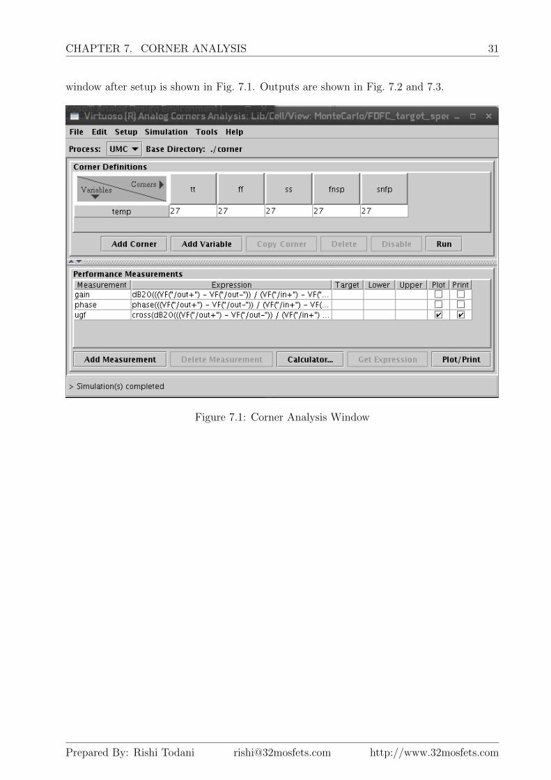
CHAPTER 7. CORNER ANALYSIS 31
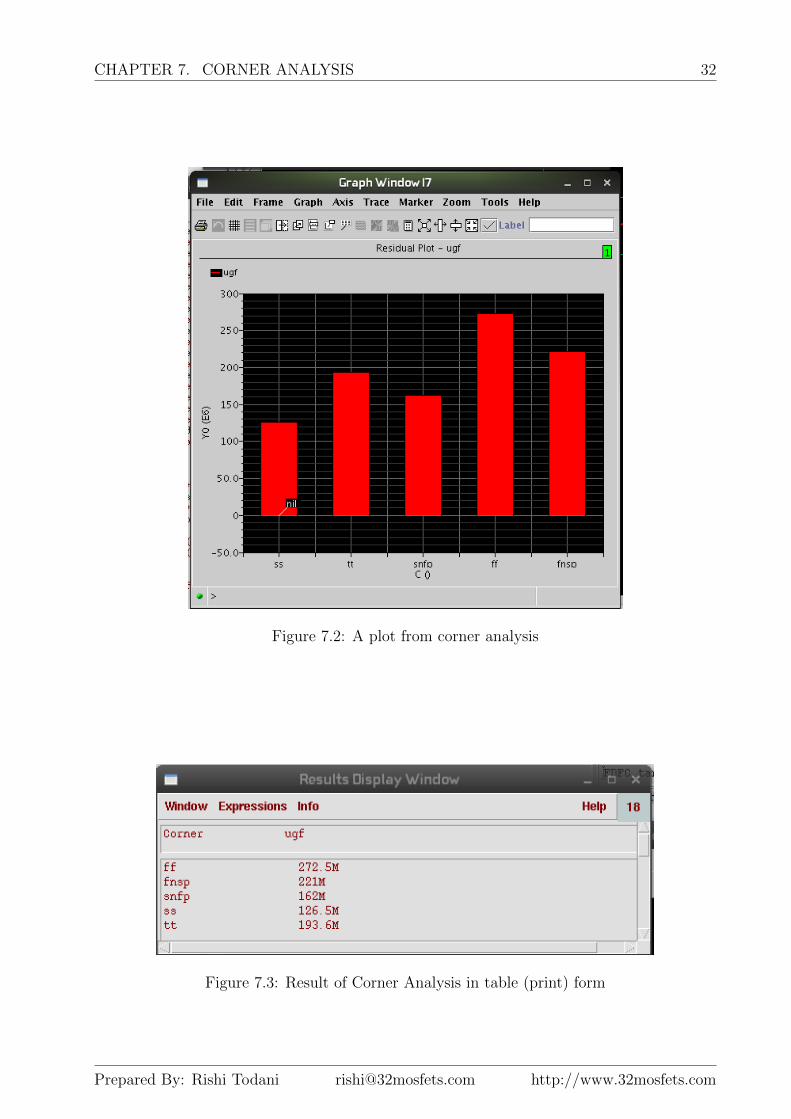
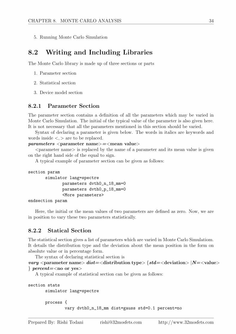
window after setup is shown in Fig. 7.1. Outputs are shown in Fig. 7.2 and 7.3.
Figure 7.1: Corner Analysis Window
Prepared By: Rishi Todani [email protected] http://www.32mosfets.com
CHAPTER 7. CORNER ANALYSIS 32
Figure 7.2: A plot from corner analysis
Figure 7.3: Result of Corner Analysis in table (print) form
Prepared By: Rishi Todani [email protected] http://www.32mosfets.com

CHAPTER
EIGHT
MONTE CARLO ANALYSIS
The Monte Carlo analysis is a swept analysis with associated child analyses similar to thesweep analysis. The Monte Carlo analysis refers to ”statistics blocks” where statisticaldistributions and correlations of netlist parameters are specified. For each iteration of theMonte Carlo analysis, new pseudo-random values are generated for the specified netlistparameters (according to their specified distributions) and the list of child analyses (like DCgain or unity gain frequency or slew rate of an amplifier) are then executed.
Expressions are associated with the child analyses. These expressions, which are con-structed as scalar calculator expressions by the user during Monte Carlo analysis set up, canbe used to measure circuit metrics, such as the slew-rate of an op-amp. During a MonteCarlo analysis, these expression results will vary as the netlist parameters vary for eachMonte Carlo iteration. The Monte Carlo analysis therefore becomes a tool that allows youto examine and predict circuit performance variations, which affect yield.
The statistics blocks allow you to specify batch-to-batch (process) and per-instance (mis-match) variations for netlist parameters. These statistically-varying netlist parameters canbe referenced by models or instances in the main netlist and may represent IC manufacturingprocess variation, or component variations for board-level designs for example.
8.1 Key Requirements to Perform Monte Carlo Simu-
lation
The Monte Carlo Simulation requires some understanding of the model libraries, the asso-ciated files and the device parameters involved. The example covered here is given withrespect to UMC 180 nm CMOS technology. Same steps are to be followed even with othertechnologies. However, correct model file has to be identified.
The key requirements for running a Monte Carlo (MC) simulation are:
1. Circuit designed in Virtuoso and its functionality verified.
2. Analysis setup for which Monte Carlo is to be carried out. For example, set up ACanalysis and setup required output if you wish to perform MC simulation to plot theunity gain frequency of an amplifier.
3. Understanding model file being used for simulation.
4. Creation of Monte Carlo library
33
CHAPTER 8. MONTE CARLO ANALYSIS 34
5. Running Monte Carlo Simulation
8.2 Writing and Including Libraries
The Monte Carlo library is made up of three sections or parts
1. Parameter section
2. Statistical section
3. Device model section
8.2.1 Parameter Section
The parameter section contains a definition of all the parameters which may be varied inMonte Carlo Simulation. The initial of the typical value of the parameter is also given here.It is not necessary that all the parameters mentioned in this section should be varied.
Syntax of declaring a parameter is given below. The words in italics are keywords andwords inside <,> are to be replaced.parameters <parameter name>=<mean value>
<parameter name> is replaced by the name of a parameter and its mean value is givenon the right hand side of the equal to sign.
A typical example of parameter section can be given as follows:
section param
simulator lang=spectre
parameters dvth0_n_18_mm=0
parameters dvth0_p_18_mm=0
<More parameters>
endsection param
Here, the initial or the mean values of two parameters are defined as zero. Now, we arein position to vary these two parameters statistically.
8.2.2 Statical Section
The statistical section gives a list of parameters which are varied in Monte Carlo Simulatiom.It details the distribution type and the deviation about the mean position in the form onabsolute value or in percentage form.
The syntax of declaring statistical section isvary <parameter name> dist=<distribution type> {std=<deviation> |N=<value>} percent=<no or yes>
A typical example of statistical section can be given as follows:
section stats
simulator lang=spectre
process {
vary dvth0_n_18_mm dist=gauss std=0.1 percent=no
Prepared By: Rishi Todani [email protected] http://www.32mosfets.com
CHAPTER 8. MONTE CARLO ANALYSIS 35
vary dvth0_p_18_mm dist=gauss std=0.1 percent=no
<More lines to vary parameters>
}
mismatch{
vary dvth0_n_18_mm dist=gauss std=0.1 percent=no
vary dvth0_p_18_mm dist=gauss std=0.1 percent=no
<More lines to vary parameters>
}
endsection stats
The parameters listed inside the process field are varied once per Monte Carlo Simulation.Whereas, parameters listed inside mismatch field are varied per every instance in the circuit.
8.2.3 Model Section
This section gives all the remaining process/device parameters necessary to carry out anysimulation. Care should be taken that the parameters mentioned in param and stats sectionshould not appear in models section. If this is not taken care, MC simulation may not run.
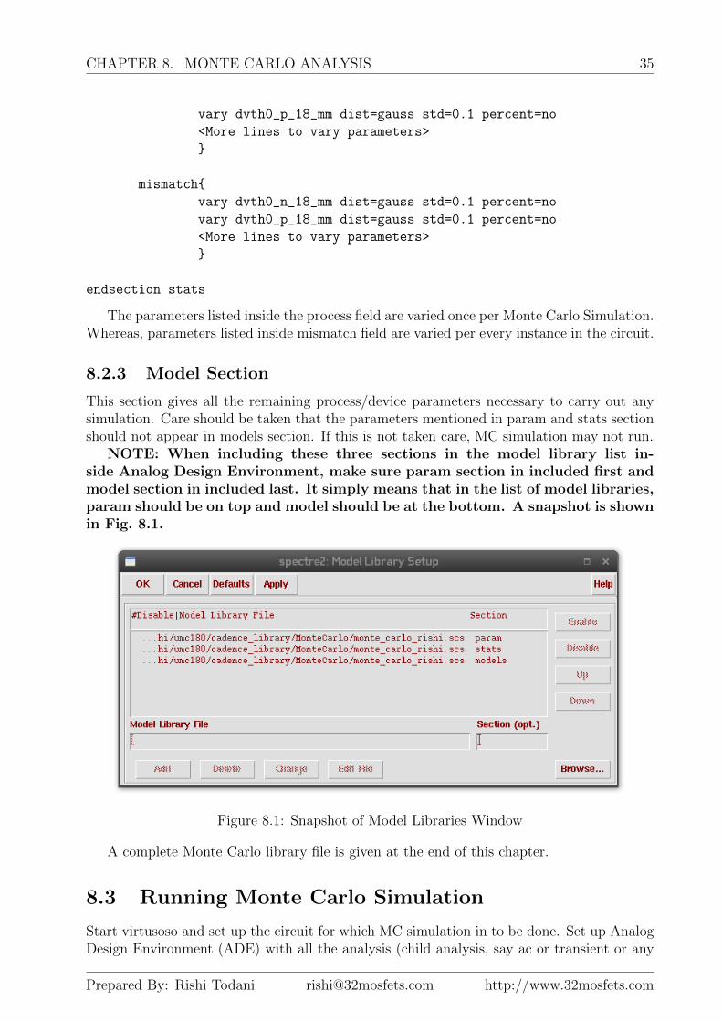
NOTE: When including these three sections in the model library list in-side Analog Design Environment, make sure param section in included first andmodel section in included last. It simply means that in the list of model libraries,param should be on top and model should be at the bottom. A snapshot is shownin Fig. 8.1.
Figure 8.1: Snapshot of Model Libraries Window
A complete Monte Carlo library file is given at the end of this chapter.
8.3 Running Monte Carlo Simulation
Start virtusoso and set up the circuit for which MC simulation in to be done. Set up AnalogDesign Environment (ADE) with all the analysis (child analysis, say ac or transient or any
Prepared By: Rishi Todani [email protected] http://www.32mosfets.com
CHAPTER 8. MONTE CARLO ANALYSIS 36
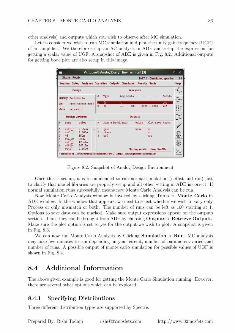
other analysis) and outputs which you wish to observe after MC simulation.Let us consider we wish to run MC simulation and plot the unity gain frequency (UGF)
of an amplifier. We therefore setup an AC analysis in ADE and setup the expression forgetting a scalar value of UGF. A snapshot of ABE is given in Fig. 8.2. Additional outputsfor getting bode plot are also setup in this image.
Figure 8.2: Snapshot of Analog Design Environment
Once this is set up, it is recommended to run normal simulation (netlist and run) justto clarify that model libraries are properly setup and all other setting in ADE is correct. Ifnormal simulation runs successfully, means now Monte Carlo Analysis can be run.
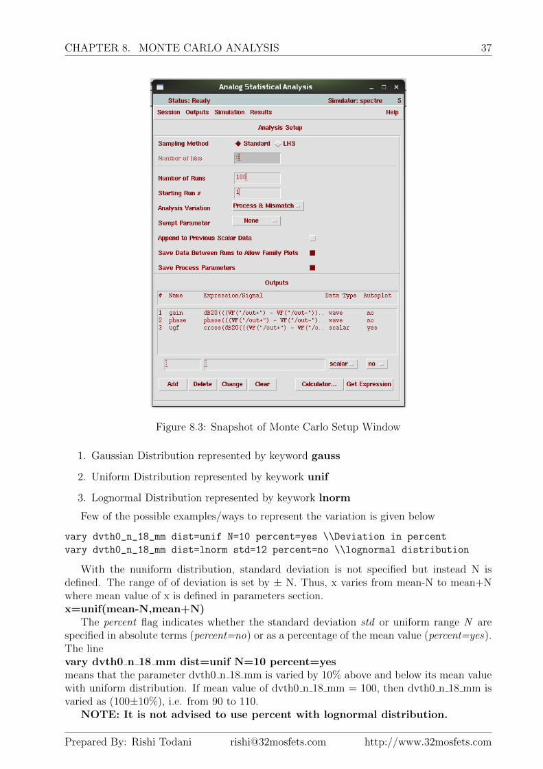
Now Monte Carlo Analysis window is invoked by clicking Tools > Monte Carlo inADE window. In the window that appears, we need to select whether we wish to vary onlyProcess or only mismatch or both. The number of runs can be left as 100 starting at 1.Options to save data can be marked. Make sure output expressions appear on the outputssection. If not, they can be brought from ADE by choosing Outputs > Retrieve Outputs.Make sure the plot option is set to yes for the output we wish to plot. A snapshot is givenin Fig. 8.3.
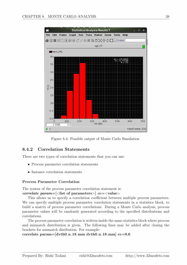
We can now run Monte Carlo Analysis by Clicking Simulation > Run. MC analysismay take few minutes to run depending on your circuit, number of parameters varied andnumber of runs. A possible output of monte carlo simulation for possible values of UGF isshown in Fig. 8.4.
8.4 Additional Information
The above given example is good for getting the Monte Carlo Simulation running. However,there are several other options which can be explored.
8.4.1 Specifying Distributions
Three different distribution types are supported by Spectre.
Prepared By: Rishi Todani [email protected] http://www.32mosfets.com
CHAPTER 8. MONTE CARLO ANALYSIS 37
Figure 8.3: Snapshot of Monte Carlo Setup Window
1. Gaussian Distribution represented by keyword gauss
2. Uniform Distribution represented by keywork unif
3. Lognormal Distribution represented by keywork lnorm
Few of the possible examples/ways to represent the variation is given below
vary dvth0_n_18_mm dist=unif N=10 percent=yes \\Deviation in percent
vary dvth0_n_18_mm dist=lnorm std=12 percent=no \\lognormal distribution
With the nuniform distribution, standard deviation is not specified but instead N isdefined. The range of of deviation is set by ± N. Thus, x varies from mean-N to mean+Nwhere mean value of x is defined in parameters section.x=unif(mean-N,mean+N)
The percent flag indicates whether the standard deviation std or uniform range N arespecified in absolute terms (percent=no) or as a percentage of the mean value (percent=yes).The linevary dvth0 n 18 mm dist=unif N=10 percent=yesmeans that the parameter dvth0 n 18 mm is varied by 10% above and below its mean valuewith uniform distribution. If mean value of dvth0 n 18 mm = 100, then dvth0 n 18 mm isvaried as (100±10%), i.e. from 90 to 110.
NOTE: It is not advised to use percent with lognormal distribution.
Prepared By: Rishi Todani [email protected] http://www.32mosfets.com
CHAPTER 8. MONTE CARLO ANALYSIS 38
Figure 8.4: Possible output of Monte Carlo Simulation
8.4.2 Correlation Statements
There are two types of correlation statements that you can use:
• Process parameter correlation statements
• Instance correlation statements
Process Parameter Correlation
The syntax of the process parameter correlation statement is:correlate param=[<list of parameters>] cc=<value>
This allows us to specify a correlation coefficient between multiple process parameters.We can specify multiple process parameter correlation statements in a statistics block, tobuild a matrix of process parameter correlations. During a Monte Carlo analysis, processparameter values will be randomly generated according to the specified distributions andcorrelations.
The process parameter correlation is written inside the same statistics block where processand mismatch distribution is given. The following lines may be added after closing thebrackets for mismatch distibution. For example:correlate param=[dvth0 n 18 mm dvth0 n 18 mm] cc=0.6
Prepared By: Rishi Todani [email protected] http://www.32mosfets.com
CHAPTER 8. MONTE CARLO ANALYSIS 39
Mismatch Correlation (Matched Devices)
The syntax of the instance or mismatch correlation statement is:correlate dev=[<list of subcircuit instances>] param=[<list of parameters>]cc=<value>
where the device or subcircuit instances to be matched are listed in the list of subcir-cuit instances, and the list of parameters specifies exactly which parameters with mismatchvariations are to be correlated.
The instance mismatch correlation statement is used to specify correlations for particularsubcircuit instances. If a subcircuit contains a device, you can effectively use the instancecorrelation statements to specify that certain devices are correlated (i.e. matched) andgive the correlation coefficient. You can optionally specify exactly which parameters areto be correlated by giving a list of parameters (each of which must have had distributionsspecified for it in a mismatch block), or specify no parameter list, in which case all parameterswith mismatch statistics specified are correlated with the given correlation coefficient. Thecorrelation coefficients are specified in the ¡value¿ field and must be between ± 1.0, notincluding 1.0 or -1.0.
The device correlation is written in a separate statistics block from one constitutingdistribution and process correlation, but inside the same section (stats). For example
statistics {
correlate dev=[M1 M2] param=[dvth0_n_18_mm dvth0_n_18_mm] cc=0.8
}
NOTE: correlation coefficients can be constants or expressions, as can stdand N when specifying distributions.
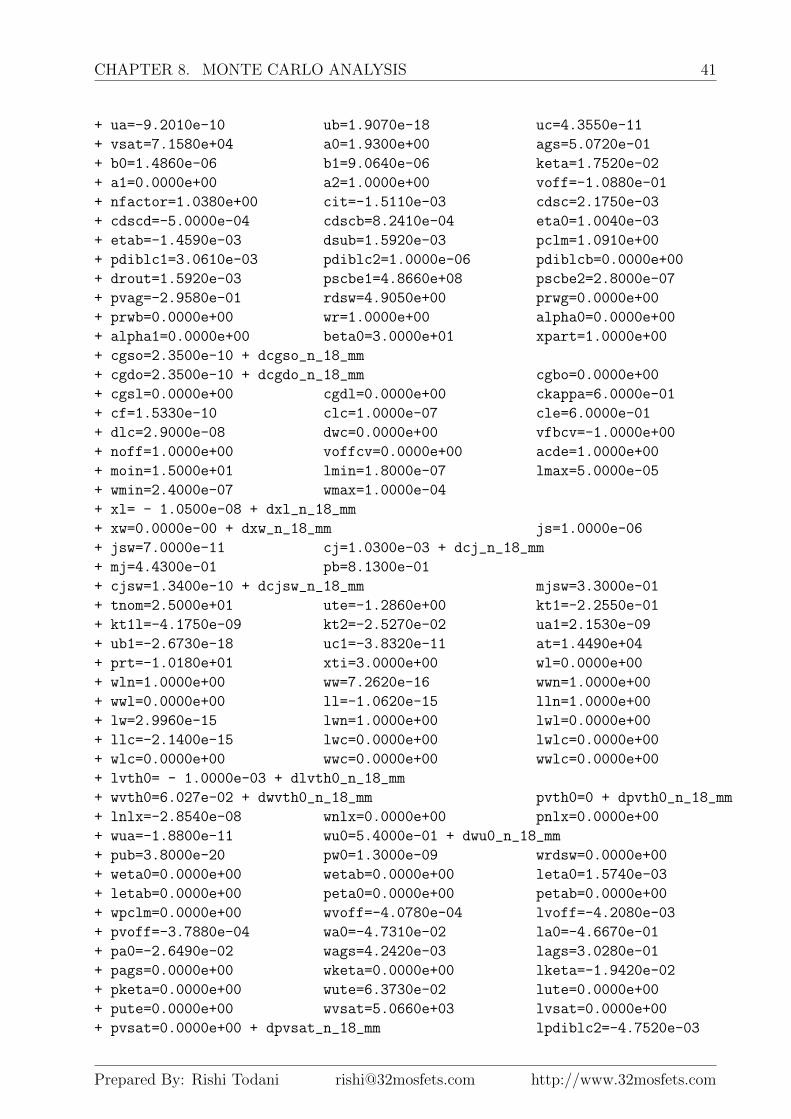
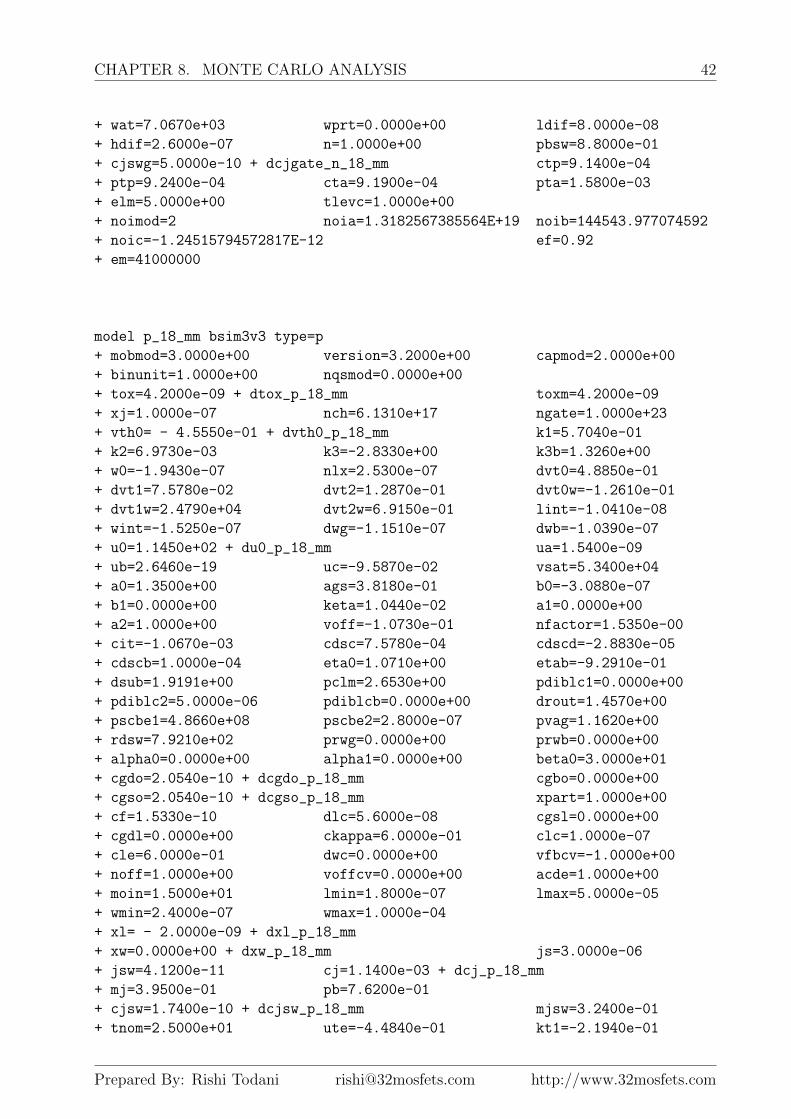
8.5 Sample Monte Carlo Library File
library monteLib
section param
simulator lang=spectre
parameters dtox_n_18_mm=0.0000e+00
parameters dxl_n_18_mm=0.0000e+00
parameters dxw_n_18_mm=0.0000e+00
parameters dvth0_n_18_mm=0.0000e+00
parameters du0_n_18_mm=0.0000e+00
parameters dlvth0_n_18_mm=0.0000e+00
parameters dwvth0_n_18_mm=0.0000e+00
parameters dwu0_n_18_mm=0.0000e+00
parameters dpvth0_n_18_mm=0.0000e+00
parameters dpvsat_n_18_mm=0.0000e+00
parameters dcgdo_n_18_mm=0.0000e+00
parameters dcgso_n_18_mm=0.0000e+00
parameters dcj_n_18_mm=0.0000e+00
parameters dcjsw_n_18_mm=0.0000e+00
parameters dcjgate_n_18_mm=0.0000e+00
Prepared By: Rishi Todani [email protected] http://www.32mosfets.com
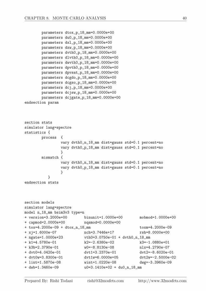
CHAPTER 8. MONTE CARLO ANALYSIS 40
parameters dtox_p_18_mm=0.0000e+00
parameters du0_p_18_mm=0.0000e+00
parameters dxl_p_18_mm=0.0000e+00
parameters dxw_p_18_mm=0.0000e+00
parameters dvth0_p_18_mm=0.0000e+00
parameters dlvth0_p_18_mm=0.0000e+00
parameters dwvth0_p_18_mm=0.0000e+00
parameters dpvth0_p_18_mm=0.0000e+00
parameters dpvsat_p_18_mm=0.0000e+00
parameters dcgdo_p_18_mm=0.0000e+00
parameters dcgso_p_18_mm=0.0000e+00
parameters dcj_p_18_mm=0.0000e+00
parameters dcjsw_p_18_mm=0.0000e+00
parameters dcjgate_p_18_mm=0.0000e+00
endsection param
section stats
simulator lang=spectre
statistics {
process {
vary dvth0_n_18_mm dist=gauss std=0.1 percent=no
vary dvth0_p_18_mm dist=gauss std=0.1 percent=no
}
mismatch {
vary dvth0_n_18_mm dist=gauss std=0.1 percent=no
vary dvth0_p_18_mm dist=gauss std=0.1 percent=no
}
}
endsection stats
section models
simulator lang=spectre
model n_18_mm bsim3v3 type=n
+ version=3.2000e+00 binunit=1.0000e+00 mobmod=1.0000e+00
+ capmod=2.0000e+00 nqsmod=0.0000e+00
+ tox=4.2000e-09 + dtox_n_18_mm toxm=4.2000e-09
+ xj=1.6000e-07 nch=3.7446e+17 rsh=8.0000e+00
+ ngate=1.0000e+23 vth0=3.0750e-01 + dvth0_n_18_mm
+ k1=4.5780e-01 k2=-2.6380e-02 k3=-1.0880e+01
+ k3b=2.3790e-01 w0=-8.8130e-08 nlx=4.2790e-07
+ dvt0=4.0420e-01 dvt1=3.2370e-01 dvt2=-8.6020e-01
+ dvt0w=3.8300e-01 dvt1w=6.0000e+05 dvt2w=-2.5000e-02
+ lint=1.5870e-08 wint=1.0220e-08 dwg=-3.3960e-09
+ dwb=1.3460e-09 u0=3.1410e+02 + du0_n_18_mm
Prepared By: Rishi Todani [email protected] http://www.32mosfets.com
CHAPTER 8. MONTE CARLO ANALYSIS 41
+ ua=-9.2010e-10 ub=1.9070e-18 uc=4.3550e-11
+ vsat=7.1580e+04 a0=1.9300e+00 ags=5.0720e-01
+ b0=1.4860e-06 b1=9.0640e-06 keta=1.7520e-02
+ a1=0.0000e+00 a2=1.0000e+00 voff=-1.0880e-01
+ nfactor=1.0380e+00 cit=-1.5110e-03 cdsc=2.1750e-03
+ cdscd=-5.0000e-04 cdscb=8.2410e-04 eta0=1.0040e-03
+ etab=-1.4590e-03 dsub=1.5920e-03 pclm=1.0910e+00
+ pdiblc1=3.0610e-03 pdiblc2=1.0000e-06 pdiblcb=0.0000e+00
+ drout=1.5920e-03 pscbe1=4.8660e+08 pscbe2=2.8000e-07
+ pvag=-2.9580e-01 rdsw=4.9050e+00 prwg=0.0000e+00
+ prwb=0.0000e+00 wr=1.0000e+00 alpha0=0.0000e+00
+ alpha1=0.0000e+00 beta0=3.0000e+01 xpart=1.0000e+00
+ cgso=2.3500e-10 + dcgso_n_18_mm
+ cgdo=2.3500e-10 + dcgdo_n_18_mm cgbo=0.0000e+00
+ cgsl=0.0000e+00 cgdl=0.0000e+00 ckappa=6.0000e-01
+ cf=1.5330e-10 clc=1.0000e-07 cle=6.0000e-01
+ dlc=2.9000e-08 dwc=0.0000e+00 vfbcv=-1.0000e+00
+ noff=1.0000e+00 voffcv=0.0000e+00 acde=1.0000e+00
+ moin=1.5000e+01 lmin=1.8000e-07 lmax=5.0000e-05
+ wmin=2.4000e-07 wmax=1.0000e-04
+ xl= - 1.0500e-08 + dxl_n_18_mm
+ xw=0.0000e-00 + dxw_n_18_mm js=1.0000e-06
+ jsw=7.0000e-11 cj=1.0300e-03 + dcj_n_18_mm
+ mj=4.4300e-01 pb=8.1300e-01
+ cjsw=1.3400e-10 + dcjsw_n_18_mm mjsw=3.3000e-01
+ tnom=2.5000e+01 ute=-1.2860e+00 kt1=-2.2550e-01
+ kt1l=-4.1750e-09 kt2=-2.5270e-02 ua1=2.1530e-09
+ ub1=-2.6730e-18 uc1=-3.8320e-11 at=1.4490e+04
+ prt=-1.0180e+01 xti=3.0000e+00 wl=0.0000e+00
+ wln=1.0000e+00 ww=7.2620e-16 wwn=1.0000e+00
+ wwl=0.0000e+00 ll=-1.0620e-15 lln=1.0000e+00
+ lw=2.9960e-15 lwn=1.0000e+00 lwl=0.0000e+00
+ llc=-2.1400e-15 lwc=0.0000e+00 lwlc=0.0000e+00
+ wlc=0.0000e+00 wwc=0.0000e+00 wwlc=0.0000e+00
+ lvth0= - 1.0000e-03 + dlvth0_n_18_mm
+ wvth0=6.027e-02 + dwvth0_n_18_mm pvth0=0 + dpvth0_n_18_mm
+ lnlx=-2.8540e-08 wnlx=0.0000e+00 pnlx=0.0000e+00
+ wua=-1.8800e-11 wu0=5.4000e-01 + dwu0_n_18_mm
+ pub=3.8000e-20 pw0=1.3000e-09 wrdsw=0.0000e+00
+ weta0=0.0000e+00 wetab=0.0000e+00 leta0=1.5740e-03
+ letab=0.0000e+00 peta0=0.0000e+00 petab=0.0000e+00
+ wpclm=0.0000e+00 wvoff=-4.0780e-04 lvoff=-4.2080e-03
+ pvoff=-3.7880e-04 wa0=-4.7310e-02 la0=-4.6670e-01
+ pa0=-2.6490e-02 wags=4.2420e-03 lags=3.0280e-01
+ pags=0.0000e+00 wketa=0.0000e+00 lketa=-1.9420e-02
+ pketa=0.0000e+00 wute=6.3730e-02 lute=0.0000e+00
+ pute=0.0000e+00 wvsat=5.0660e+03 lvsat=0.0000e+00
+ pvsat=0.0000e+00 + dpvsat_n_18_mm lpdiblc2=-4.7520e-03
Prepared By: Rishi Todani [email protected] http://www.32mosfets.com
CHAPTER 8. MONTE CARLO ANALYSIS 42
+ wat=7.0670e+03 wprt=0.0000e+00 ldif=8.0000e-08
+ hdif=2.6000e-07 n=1.0000e+00 pbsw=8.8000e-01
+ cjswg=5.0000e-10 + dcjgate_n_18_mm ctp=9.1400e-04
+ ptp=9.2400e-04 cta=9.1900e-04 pta=1.5800e-03
+ elm=5.0000e+00 tlevc=1.0000e+00
+ noimod=2 noia=1.3182567385564E+19 noib=144543.977074592
+ noic=-1.24515794572817E-12 ef=0.92
+ em=41000000
model p_18_mm bsim3v3 type=p
+ mobmod=3.0000e+00 version=3.2000e+00 capmod=2.0000e+00
+ binunit=1.0000e+00 nqsmod=0.0000e+00
+ tox=4.2000e-09 + dtox_p_18_mm toxm=4.2000e-09
+ xj=1.0000e-07 nch=6.1310e+17 ngate=1.0000e+23
+ vth0= - 4.5550e-01 + dvth0_p_18_mm k1=5.7040e-01
+ k2=6.9730e-03 k3=-2.8330e+00 k3b=1.3260e+00
+ w0=-1.9430e-07 nlx=2.5300e-07 dvt0=4.8850e-01
+ dvt1=7.5780e-02 dvt2=1.2870e-01 dvt0w=-1.2610e-01
+ dvt1w=2.4790e+04 dvt2w=6.9150e-01 lint=-1.0410e-08
+ wint=-1.5250e-07 dwg=-1.1510e-07 dwb=-1.0390e-07
+ u0=1.1450e+02 + du0_p_18_mm ua=1.5400e-09
+ ub=2.6460e-19 uc=-9.5870e-02 vsat=5.3400e+04
+ a0=1.3500e+00 ags=3.8180e-01 b0=-3.0880e-07
+ b1=0.0000e+00 keta=1.0440e-02 a1=0.0000e+00
+ a2=1.0000e+00 voff=-1.0730e-01 nfactor=1.5350e-00
+ cit=-1.0670e-03 cdsc=7.5780e-04 cdscd=-2.8830e-05
+ cdscb=1.0000e-04 eta0=1.0710e+00 etab=-9.2910e-01
+ dsub=1.9191e+00 pclm=2.6530e+00 pdiblc1=0.0000e+00
+ pdiblc2=5.0000e-06 pdiblcb=0.0000e+00 drout=1.4570e+00
+ pscbe1=4.8660e+08 pscbe2=2.8000e-07 pvag=1.1620e+00
+ rdsw=7.9210e+02 prwg=0.0000e+00 prwb=0.0000e+00
+ alpha0=0.0000e+00 alpha1=0.0000e+00 beta0=3.0000e+01
+ cgdo=2.0540e-10 + dcgdo_p_18_mm cgbo=0.0000e+00
+ cgso=2.0540e-10 + dcgso_p_18_mm xpart=1.0000e+00
+ cf=1.5330e-10 dlc=5.6000e-08 cgsl=0.0000e+00
+ cgdl=0.0000e+00 ckappa=6.0000e-01 clc=1.0000e-07
+ cle=6.0000e-01 dwc=0.0000e+00 vfbcv=-1.0000e+00
+ noff=1.0000e+00 voffcv=0.0000e+00 acde=1.0000e+00
+ moin=1.5000e+01 lmin=1.8000e-07 lmax=5.0000e-05
+ wmin=2.4000e-07 wmax=1.0000e-04
+ xl= - 2.0000e-09 + dxl_p_18_mm
+ xw=0.0000e+00 + dxw_p_18_mm js=3.0000e-06
+ jsw=4.1200e-11 cj=1.1400e-03 + dcj_p_18_mm
+ mj=3.9500e-01 pb=7.6200e-01
+ cjsw=1.7400e-10 + dcjsw_p_18_mm mjsw=3.2400e-01
+ tnom=2.5000e+01 ute=-4.4840e-01 kt1=-2.1940e-01
Prepared By: Rishi Todani [email protected] http://www.32mosfets.com
CHAPTER 8. MONTE CARLO ANALYSIS 43
+ kt1l=-8.2040e-09 kt2=-9.4870e-03 ua1=4.5710e-09
+ ub1=-6.0260e-18 uc1=-9.8500e-02 at=1.2030e+04
+ prt=0.0000e+00 xti=3.0000e+00 ww=1.2360e-14
+ lw=-2.8730e-16 ll=6.6350e-15 wl=0.0000e+00
+ wln=1.0000e+00 wwn=1.0000e+00 wwl=0.0000e+00
+ lln=1.0000e+00 lwn=1.0000e+00 lwl=0.0000e+00
+ llc=-7.4500e-15 lwc=0.0000e+00 lwlc=0.0000e+00
+ wlc=0.0000e+00 wwc=0.0000e+00 wwlc=0.0000e+00
+ lvth0=4.4000e-03 + dlvth0_p_18_mm
+ wvth0= - 1.4800e-02 + dwvth0_p_18_mm
+ pvth0=3.2000e-03 + dpvth0_p_18_mm lnlx=-1.5840e-08
+ wrdsw=1.0070e+01 weta0=0.0000e+00 wetab=0.0000e+00
+ wpclm=0.0000e+00 wua=2.6300e-09 lua=-8.1530e-11
+ pua=5.8550e-11 wub=0.0000e+00 lub=0.0000e+00
+ pub=0.0000e+00 wuc=0.0000e+00 luc=0.0000e+00
+ puc=0.0000e+00 wvoff=-9.8160e-03 lvoff=-9.8710e-04
+ pvoff=-9.8330e-05 wa0=-4.8070e-02 la0=-2.8100e-01
+ pa0=8.6610e-02 wags=-4.1770e-02 lags=4.4540e-02
+ pags=-4.0760e-02 wketa=0.0000e+00 lketa=-1.2000e-02
+ pketa=0.0000e+00 wute=-2.6820e-01 lute=0.0000e+00
+ pute=0.0000e+00 wvsat=-1.4200e+04 lvsat=0.0000e+00
+ pvsat= - 4.3400e+02 + dpvsat_p_18_mm lpdiblc2=3.0120e-03
+ cjswg=4.200e-10 + dcjgate_p_18_mm wat=-6.4050e+03
+ wprt=2.1660e+02 n=1.0000e+00 pbsw=6.6500e-01
+ cta=1.0000e-03 ctp=7.5300e-04 pta=1.5500e-03
+ ptp=1.2400e-03 ldif=8.0000e-08 rsh=8.0000e+00
+ rd=0.0000e+00 rsc=0.0000e+00 rdc=0.0000e+00
+ hdif=2.6000e-07 rs=0.0000e+00
+ noimod=2 noia=3.57456993317604E+18 noib=2500
+ noic=2.61260020285845E-11 ef=1.1388
+ em=41000000
endsection models
endlibrary monteLib
Prepared By: Rishi Todani [email protected] http://www.32mosfets.com