Embed Size (px)
Citation preview

5
A Torus-Based Hierarchical Optical-Electronic Network-on-Chipfor Multiprocessor System-on-Chip
YAOYAO YE, JIANG XU, and XIAOWEN WU, The Hong Kong University of Science and TechnologyWEI ZHANG, Nanyang Technological UniversityWEICHEN LIU and MAHDI NIKDAST, The Hong Kong University of Science and Technology
Networks-on-chip (NoCs) are emerging as a key on-chip communication architecture for multiprocessorsystems-on-chip (MPSoCs). Optical communication technologies are introduced to NoCs in order to em-power ultra-high bandwidth with low power consumption. However, in existing optical NoCs, communica-tion locality is poorly supported, and the importance of floorplanning is overlooked. These significantly limitthe power efficiency and performance of optical NoCs. In this work, we address these issues and propose atorus-based hierarchical hybrid optical-electronic NoC, called THOE. THOE takes advantage of both elec-trical and optical routers and interconnects in a hierarchical manner. It employs several new techniquesincluding floorplan optimization, an adaptive power control mechanism, low-latency control protocols, andhybrid optical-electrical routers with a low-power optical switching fabric. Both of the unfolded and foldedtorus topologies are explored for THOE. Based on a set of real MPSoC applications, we compared THOE witha typical torus-based optical NoC as well as a torus-based electronic NoC in 45nm on a 256-core MPSoC, us-ing a SystemC-based cycle-accurate NoC simulator. Compared with the matched electronic torus-based NoC,THOE achieves 2.46X performance and 1.51X network switching capacity utilization, with 84% less energyconsumption. Compared with the optical torus-based NoC, THOE achieves 4.71X performance and 3.05Xnetwork switching capacity utilization, while reducing 99% of energy consumption. Besides real MPSoCapplications, a uniform traffic pattern is also used to show the average packet delay and network through-put of THOE. Regarding hardware cost, THOE reduces 75% of laser sources and half of optical receiverscompared with the optical torus-based NoC.
Categories and Subject Descriptors: C.1.2 [Processor Architectures]: Multiple Data Stream Architec-tures (Multiprocessors)—Interconnection architectures, Parallel processors
General Terms: Design, Performance
Additional Key Words and Phrases: Hierarchical architecture, multiprocessor system-on-chip, opticalnetwork-on-chip, optical-electronic router, power consumption
ACM Reference Format:Ye, Y., Xu, J., Wu, X., Zhang, W., Liu, W., and Nikdast, M. 2012. A torus-based hierarchical optical-electronicnetwork-on-chip for multiprocessor system-on-chip. ACM J. Emerg. Technol. Comput. Syst. 8, 1, Article 5(February 2012), 26 pages.DOI = 10.1145/2093145.2093150 http://doi.acm.org/2093145.2093150
This work is partially supported by HKUST RPC and RGC of the Hong Kong Special Administrative Region,China.Authors’ addresses: Y. Ye, J. Xu, X. Wu, W. Liu, and M. Nikdast, Electronic and Computer Engineering De-partment, The Hong Kong University of Science and Technology, Hong Kong; W. Zhang, School of ComputerEngineering, Nanyang Technological University, Singapore; email: [email protected] to make digital or hard copies of part or all of this work for personal or classroom use is grantedwithout fee provided that copies are not made or distributed for profit or commercial advantage and thatcopies show this notice on the first page or initial screen of a display along with the full citation. Copyrightsfor components of this work owned by others than ACM must be honored. Abstracting with credit is permit-ted. To copy otherwise, to republish, to post on servers, to redistribute to lists, or to use any component ofthis work in other works requires prior specific permission and/or a fee. Permissions may be requested fromthe Publications Dept., ACM, Inc., 2 Penn Plaza, Suite 701, New York, NY 10121-0701, USA, fax +1 (212)869-0481, or [email protected]© 2012 ACM 1558-4832/2012/02-ART5 $10.00
DOI 10.1145/2093145.2093150 http://doi.acm.org/10.1145/2093145.2093150
ACM Journal on Emerging Technologies in Computing Systems, Vol. 8, No. 1, Article 5, Publication date: February 2012.

5:2 Y. Ye et al.
1. INTRODUCTION
With the increasing complexity of multiprocessor systems-on-chip (MPSoCs), tensof intellectual property (IP) cores could be integrated on a single chip. The growingon-chip communication demands put tremendous pressure on global interconnec-tions, and it has become a major challenge for MPSoC performance improvementunder restricted energy budgets. An efficient communication architecture can helpto fully utilize the increasing computation resources and maximize MPSoC perfor-mance. Networks-on-chip (NoCs) are emerging as a promising infrastructure foron-chip communication of MPSoCs [Benini and De Micheli 2001, 2002; Dally andTowles 2001; Kumar et al. 2002; Rijpkema et al. 2003; Xu et al. 2005]. Instead ofrouting design-specific global interconnects, information is exchanged by routingpackets in the network based on modern networking theories. The better scalabilityand design reusability make NoCs more favorable than traditional bus or ad hocarchitectures [Lee et al. 2007].
In deep submicron (DSM) VLSI technologies, copper-based metallic intercon-nects are becoming increasingly susceptible to parasitic resistance and capacitance[Pasricha and Dutt 2008]. Both chip-to-chip and on-chip global interconnects are fac-ing serious problems of delay, power consumption, and electromagnetic interference(EMI). As feature sizes continue to decrease, metallic interconnects would consumesignificant amounts of power to deliver the higher communication bandwidth requiredin the near future, and electronic NoCs may not be able to satisfy future performancerequirements under power restrictions. On the other hand, optics offers fundamentalphysical advantages to overcome the limitations faced by electrical interconnects.Optical NoCs were proposed to take advantage of optical technologies and reduceoverall interconnect power dissipation. They also provide ultra high bandwidth tokeep pace with transistor speeds [Cho et al. 2004]. Such optical solutions are madepossible by recent developments in nanoscale silicon photonics and monolithicallyintegrated optical devices; an energy efficiency near 1pJ/bit will be achieved for TB/sdata rates [Chen et al. 2007; Masini et al. 2007; Perkins and Fonstad 2007; Perkinset al. 2008; Yin et al. 2007; Young et al. 2009].
Though optical NoCs offer a new approach to empower bandwidth increase withlow power, there are several issues to be considered. First, communication locality ispoorly supported in traditional mesh and torus based optical NoCs. In nonhierarchicalnetworks, such as generic mesh and torus, short- and long-distance traffic interferewith each other and cause low network utilization and large communication latency.Second, an optical circuit switching mechanism is effective for long-distance traffic, butfor short-distance traffic, the overhead of circuit switching limits the communicationefficiency. Third, the floorplans of optical NoCs are largely overlooked. A networktopology can indicate many possible floorplans to physically implement an optical NoCon a chip. An optimized floorplan can maximize the network performance and energyefficiency of an optical NoC.
To address these issues, we propose a torus-based hierarchical hybrid optical-electronic NoC, called THOE, in this work. THOE utilizes both electronic and opticalinterconnects in a hierarchical manner through novel hybrid optical-electrical routerdesigns. It employs several new techniques including floorplan optimization, an adap-tive power control mechanism, low-latency control protocols, and a new low-power op-tical switching fabric. Based on a set of real MPSoC applications, we compared THOEwith torus-based optical NoC as well as a torus-based electronic NoC in 45nm on a256-core MPSoC, using a SystemC-based cycle-accurate NoC simulator. Comparedwith the electronic torus-based NoC, THOE achieves 2.46X performance and 1.51Xnetwork switching capacity utilization, with 84% less energy consumption. Compared
ACM Journal on Emerging Technologies in Computing Systems, Vol. 8, No. 1, Article 5, Publication date: February 2012.
A Torus-Based Hierarchical Optical-Electronic NoC for Multiprocessor SoC 5:3
with the torus-based optical NoC, THOE achieves 4.71X performance and 3.05X net-work switching capacity utilization, while reducing 99% of energy consumption.
The rest of the article is organized as follows. Section 2 gives a survey of the relatedwork on optical NoCs. Section 3 details THOE, including the architecture and pro-tocols. Simulation results are then analyzed in Section 4. We compared THOE witha torus-based optical NoC as well as a torus-based electronic NoC in terms of perfor-mance, energy consumption and the network switching capacity utilization. Section 5draws the conclusions of this work.
2. PREVIOUS WORK
Several on-chip optical interconnection networks have been proposed in the litera-ture. Shacham et al. [2008] proposed a circuit-switched augmented folded torus net-work based on 4 × 4 optical switches. Gu et al. [2008] proposed an optical mesh withlow power loss and cost. Petracca et al. [2008] proposed a nonblocking crossbar and anonblocking mesh for chip multiprocessors (CMPs), and showed that the nonblockingmesh achieves better throughput. Kash [2007] proposed an intrachip optical networkICON, using three-dimensional integration technology. The photonic NoC is combinedwith a separate multiprocessor plane, which allows electronic and photonics planes tobe optimized separately. Kirman and Martınez [2010] proposed an all-optical networkfor CMPs. Multiple optical network layers are used to increase bandwidth, and for thebenefit of design simplicity and power efficiency, wavelength allocation and routingpattern are all set at design time. Cianchetti et al. [2009] proposed an optical routingnetwork, called Phastlane, for large-scale cache coherent microprocessors. Low-latencynanophotonics is exploited to make packets traverse several hops under contentionlessconditions.
In order to facilitate local traffic, some photonic NoC architectures are designed toutilize electrical interconnects for fast local switching. Batten et al. [2008] proposedan optical NoC with global crossbar topology. Processing cores and DRAM are dividedinto and connected with a hybrid optoelectrical global optical crossbar. Vantreaseet al. [2008] proposed a clustered optical interconnection network, called Corona, withbroadcasting support. The clusters communicate through a single-read-multiple-writeoptical crossbar and an optical broadcast bus. Pan et al. [2009] proposed two opticalcrossbar architectures for global communication, including a distributed crossbarFirefly and an improved crossbar called Flexishare [Pan et al. 2010]. Flexishareminimizes static power consumption by sharing a reduced number of channels acrossthe network. Kirman et al. [2006] proposed a hierarchical optoelectrical system, inwhich cores are interconnected with an optical ring with WDM (wavelength divisionmultiplexing) support. Each core is assigned a set of unique wavelengths for opticalcommunication. Morris and Kodi [2010] proposed a scalable 64-core NoC design calledPROPEL. Each four cores are combined through a shared L2 cache, and photonicinterconnects are used for interrouter communication. Bahirat and Pasricha [2009]proposed a hybrid photonic NoC using a photonic ring waveguide to enhance the per-formance of a traditional electronic mesh. A photonic path would be chosen instead of atraditional XY route in the electronic mesh for long distance communication. In orderto fully exploit the benefits of optical switching for realistic CMP applications, Artundoet al. [2009] introduced a reconfigurable optical interconnect that can be adapted auto-matically to the traffic situation. A hybrid photonic NoC communication architectureUC-PHOTON is designed to cope with the variable bandwidth and latency constraintsof multiple use-case applications implemented on CMPs [Bahirat and Pasricha 2010].
For optical router design, microresonators (MRs) of different structures are com-monly used to perform the switching function. 1x2 all-optical comb switching wasdemonstrated for WDM applications by using a 200μm-diameter ring resonator [Dong
ACM Journal on Emerging Technologies in Computing Systems, Vol. 8, No. 1, Article 5, Publication date: February 2012.

5:4 Y. Ye et al.
et al. 2007]. The demonstrated switch has a switching time of less than 1ns. A non-blocking 4 × 4 switch was proposed in Shacham et al. [2008]. The nonblocking char-acteristic guarantees an internal path from any input port to any output port, as longas no two packets are contending for the same output port and no U-turn is allowed.A passive-switching NxN λ-router with high scalability was proposed based on WDMtechnology [Briere et al. 2007]. A 5 × 5 optical switching fabric was demonstrated byPoon et al. [2008]. Experimental results show that the on-off switching power con-sumption for establishing a light path in a single switch node is only on the orderof 20μW. A low-power non-blocking optical router, Cygnus, was proposed in Gu et al.[2009]. It was demonstrated that while using a dimension order routing algorithm,the maximum power consumption to send a packet through a network is a small con-stant value, regardless of the network size. An ultracompact wavelength-insensitiveoptical switch was proposed based on cascaded silicon MRs [Vlasov et al. 2008]. Theswitch is capable of simultaneous error-free switching of a large number of 40Gbpsbandwidth channels with minimal power penalties of less than 0.3dB. A nonblockingfour-port photonic router was demonstrated with three 10Gbps wavelength-parallelchannels [Biberman et al. 2010]. In addition, some research work has been done toimprove the spectrum response of microresonator-based switching filters for WDM ap-plications. In order to get a broader passband and higher extinction ratio, multistageracetrack resonators can be used to replace the single-ring design [Chen et al. 2010].
The technological and device aspects of integrated optical interconnect for on-chipdata transport was first presented in O’Connor et al. [2006]. A source-based opticalinterconnect using heterogeneous integration was proposed to achieve an above-IC op-tical transport layer. A CMOS driver circuit modulates the current flowing throughthe laser source, and controls the power of the emitted light. Optical signals generatedby the laser source propagate to the receiver through a waveguide. A typical receiverincludes a photodetector as well as transimpedance amplifier (TIA) and limiting am-plifier (LA) circuits [Kromer et al. 2005]. The photodetector converts optical signalsinto electrical current which is then converted to electrical voltage by TIA. The sub-sequent LAs amplify the electrical voltage to the logic level [O’Connor et al. 2006].High-speed, low-power and small feature-size electronics and optical components areboth required for optical links. Based on the rapid technology advances in recent years,VCSELs (vertical cavity surface emitting laser) provide an opportunity for better inte-gration and are used by many optical NoC architectures to fully integrate optical NoCson chip multiprocessors. VCSELs can be directly modulated by driving current. Theyare suitable for optical interconnects because of their low power consumption, highmodulation bandwidth, and manufacturing advantages. VCSELs for commercial opti-cal transceivers currently operate at up to 10Gbps per channel, in VCSEL array formwith up to 12 parallel channels per module [Ji et al. 2009]. 10Gbps VCSELs with highsingle-mode output in excess of 4mW at room temperature have been demonstrated inthe 1550nm band [Syrbu et al. 2008]. By using heterogeneous integration techniquessuch as recess mounting with monolithic metallization integration, standardly fabri-cated VCSELs can be fully integrated within the dielectric stack of CMOS integratedcircuits to improve transfer rates in high-performance circuit applications [Perkinsand Fonstad 2007; Perkins et al. 2008]. Each VCSEL pill has a diameter of 55μm. Theintegration can be done by first removing the native GaAs substrate and then placingmetal contact and bonding layers on the bottom. For photodetectors, most of the cur-rent research is focused on using Ge as the absorbing material because of their muchhigher absorption coefficient in the near infrared and their compatibility with stan-dard CMOS processing. A 1550nm optical receiver achieves a sensitivity of −14.2dBmfor a 10−12 bit error rate (BER) at a data rate of 10Gbps, using Ge waveguide pho-todetectors monolithically integrated in a 130nm CMOS process [Masini et al. 2007].
ACM Journal on Emerging Technologies in Computing Systems, Vol. 8, No. 1, Article 5, Publication date: February 2012.

A Torus-Based Hierarchical Optical-Electronic NoC for Multiprocessor SoC 5:5
Fig. 1. THOE architecture.
Another work reported a better receiver sensitivity of −18.9dBm for the same BER ata lower data rate of 5Gbps [Zheng et al. 2010].
3. THOE
In this section, THOE is detailed, including its hierarchical architecture, optimizedfloorplan, hybrid optical-electronic router design, network protocols and power controlmechanism.
3.1. THOE Architecture
THOE utilizes both optical and electrical interconnects to connect processors in a hi-erarchical architecture (Figure 1). Each four processors are grouped into a clusterthrough an electronic switching fabric, and all the clusters are interconnected by aunfolded or folded torus network through optical switching fabrics and optical waveg-uides. Processors in the same cluster share a hierarchical router that includes thelocal electronic switching fabric, optical switching fabric, and a control unit. Both theelectronic and optical Switching fabrics are controlled by the control unit. Traffic in-side a cluster is delivered through the local electronic switching fabric, and long-rangecommunications are transferred through the global optical network. An overlappedelectronic control network is used to maintain optical paths. Each cluster has a uniqueID for addressing, and each processor is assigned a main ID and sub ID pair. The mainID is used to identify a cluster and the sub ID is used to identify a processor within acluster. The topology of an optical NoC may not directly indicate the optimal physicalfloorplan; the physical floorplan can be optimized by carefully arranging waveguidesand I/O ports of routers to minimize the waveguide crossings in the network. The op-timized floorplan can reduce THOE’s power consumption; its details will be discussedin the next section. THOE takes advantage of electronic switching for local traffic andan optical network for long-range traffic. The hierarchical structure also reduces net-work contentions due to traffic interference. This helps to improve performance; thedetailed simulation results will be analyzed in the next section.
In THOE, the hybrid optical-electronic router implements routing and flow controlfunctions. As shown in Figure 1 (c), it consists of an electronic switching fabric (ESF),an optical switching fabric (OSF), a router control unit (RCU), an adaptive power con-trol unit (APCU), and an O/E interface. RCU controls both the ESF and OSF andimplements control logic and protocols. ESF is a 5 × 5 nonblocking input-bufferedelectronic crossbar that is used for intracluster communication. It connects four localprocessors and an O/E interface. O/E interfaces handle serialization, OE/EO conver-sion, and deserialization. APCU implements the adaptive power control mechanism
ACM Journal on Emerging Technologies in Computing Systems, Vol. 8, No. 1, Article 5, Publication date: February 2012.

5:6 Y. Ye et al.
Fig. 2. Crux optical switching fabric and two basic switching elements.
and uses the routing information to adjust O/E conversions. The power control mech-anism will be explained later.
We designed a compact low-loss 5 × 5 strictly nonblocking optical switching fabric,called Crux (Figure 2), for the hybrid router. The five bidirectional ports include in-jection/ejection, east, south, west, and north ports. They are aligned to their intendeddirections so no extra crossings will be incurred in the floorplan. Input and output ofeach port are also properly aligned. The injection/ejection ports are used to connect theESF through an O/E interface. Crux is constructed based on two basic switching ele-ments, both of which consist of two optical waveguides and one MR. The only differenceis the position of the two waveguides. Light signals can propagate along the waveg-uide and/or be switched to another direction by the MR. The MR has different on-stateand off-state resonance wavelengths. If the input light has the same wavelength asthe MR, it would be coupled into the MR and directed to the drop port. Otherwise, thelight would propagate directly to the through port. Multiple basic switching elementsmay be combined to implement predefined switching functions. By turning on/off MRsproperly, the injected optical signal can be controlled to propagate from an input portto an output port. MRs used in Crux are assumed to be resonating at the 1550nmband when they are turned on. The fabrication is based on silicon waveguides with500nm × 200nm cross-section and the insertion loss of about 0.5dB [Xiao et al. 2007].The MR has a diameter of about 10μm. An optical terminator is an important butexpensive device used in the open end of an optical link. Its function is to absorb lightand prevent light from returning to the transmission line. In a 5 × 5 optical crossbar,five horizontal waveguides are crossed with five vertical waveguides. Each waveguidehas two ends, one of which is used as input/output and the other is open-ended. As aresult, ten optical terminators are needed for a 5 × 5 optical crossbar, with one in theopen end of each waveguide. Crux reduces the number of optical terminators to three,and thus reduces system cost.
Crux takes advantage of the parallel switching element to minimize the waveguidecrossing insertion loss. For example, the two waveguides for the injection/ejectionport only use the parallel switching elements. The maximum number of crossingsper link from any input port to any output port is five. This feature is beneficial forreducing the total optical power loss, especially for optical NoCs with a large diameter.In addition, Crux can passively route optical signals. During passive routing, Cruxdoes not need to turn on any MR if an optical signal travels in only one directionthrough the router, such as from north to south or from west to east. Only one MRwill be powered on if an optical signal turns from one direction to another direction
ACM Journal on Emerging Technologies in Computing Systems, Vol. 8, No. 1, Article 5, Publication date: February 2012.

A Torus-Based Hierarchical Optical-Electronic NoC for Multiprocessor SoC 5:7
Fig. 3. Torus topology.
Fig. 4. The optimized floorplan of unfolded torus.
or uses the injection/ejection port. Because of this property, at most three MRs will bepowered on any optical path regardless of the THOE network size.
3.2. Topology and Optimized Floorplan
THOE uses torus topology. Regular topologies, such as mesh and torus, are preferredby NoCs because of the predictable scalability in terms of performance and power con-sumption [Balfour and Dally 2006; Bjerregaard and Mahadevan 2006; Pande et al.2005]. As distinguished from mesh topology, the torus takes advantage of the wrap-around links among edge nodes to offer better path diversity and better load balance.Figure 3 shows the unfolded and folded torus topologies. Compared with unfoldedtorus topology, folded torus achieves more balanced hop latency and avoids extra en-ergy consumption in the wrap-around channels.
The optimized floorplans (Figure 4, Figure 5) maintain the connection propertyshown in the unfolded and folded torus topologies, but minimize the number of waveg-uide crossings in physical implementations. Waveguide crossings in optical NoCs donot affect the bandwidth, but cause more loss and power consumption during packettransmission. In optical NoCs, each waveguide crossing introduces about 0.12dB inser-tion loss to the passing optical signals [Poon et al. 2008]. A large number of waveguide
ACM Journal on Emerging Technologies in Computing Systems, Vol. 8, No. 1, Article 5, Publication date: February 2012.

5:8 Y. Ye et al.
Fig. 5. The optimized floorplan of a folded torus.
crossings in an optical transmission path would result in significant optical power loss.To minimize power loss in optical NoCs, it is desired to reduce the number of waveg-uide crossings within the whole network. However, the topology of an optical NoC maynot directly indicate the optimal physical floorplan. In order to minimize waveguidecrossings in the network level, THOE optimizes the floorplans for both the unfoldedand folded torus-based optical NoCs by rearranging the waveguides and I/O ports ofthe optical routers.
We analyzed the number of waveguide crossings in the topology and the optimizedfloorplan for both the MxN unfolded and folded torus-based optical NoCs. Here we as-sume the links between routers are unidirectional, and there is only one waveguide ineach link. Equation (1) shows the number of waveguide crossings in the MxN unfoldedtorus topology.
Cut = 3MN − 4M − 4N + 8. (1)Equation (2) gives the number of waveguide crossings in the optimized floorplan of theMxN unfolded torus-based optical NoC.
Cuf = MN − 2 ∗ max(M, N). (2)
Equations (1) and (2) show that waveguide crossings in the unfolded torus-based op-tical NoC are effectively reduced through floorplan optimization. For example, in an8 × 8 unfolded torus-based optical NoC, the total number of waveguide crossings inthe topology is 136, and the optimized floorplan reduces it to 48. The reduction can beeven more effective as M and N are increasing.
For the folded torus, we find that the number of waveguide crossings depends noton only M and N but also their parities due to different network arrangements. Equa-tion (3) shows the number of waveguide crossings in the MxN folded torus topology.
C ft =
{3MN − 2M − 2N, If M, N are even3MN − 2M − 2N + 2, Otherwise
. (3)
Equation (4) gives the number of waveguide crossings in the optimized floorplan of theMxN folded torus-based optical NoC.
C f f =
{3MN − 4M − 4N, If M, N are even3MN − 4M − 4N + 2, Otherwise
. (4)
ACM Journal on Emerging Technologies in Computing Systems, Vol. 8, No. 1, Article 5, Publication date: February 2012.

A Torus-Based Hierarchical Optical-Electronic NoC for Multiprocessor SoC 5:9
Equations 3 and 4 show that waveguide crossings in the MxN folded torus-basedoptical NoC can be reduced by 2(M + N) through floorplan optimization. For example,in an 8 × 8 folded torus-based optical NoC, the number of waveguides crossings in thetopology is 160, and the optimized floorplan reduces it to 128.
The floorplan optimization works better for the unfolded torus-based optical NoC,with fewer waveguide crossings than the folded one. On the other hand, folded torustopology has more balanced hop-length than the unfolded one by folding the wholenetwork. This advantage is more obvious in the optimized floorplans. In the opti-mized unfolded torus-based optical NoC, the longest waveguide is nearly half of thechip perimeter and is much longer than the longest waveguide in the folded one. Incurrent technology, waveguide propagation loss is about 0.17dB/mm [Xia et al. 2007].In a 10mm × 10mm2 chip, the long wraparound waveguide in the optimized unfoldedtorus optical NoC will thus induce about 3.4dB optical power loss for passing signals.So the unfolded and folded torus-based optical NoCs have their own advantages anddisadvantages, and there is a trade-off between the number of waveguide crossingsand the longest waveguide length.
3.3. Protocols
In THOE, electronic packet switching and optical circuit switching are combined in ahierarchical manner to offer better communication efficiency. For a packet waiting inthe head of the input buffer of ESF, RCU will examine its destination to determinewhether it is intra or inter-cluster traffic. If it is intracluster, RCU will forward it tothe corresponding output port through the ESF. If the desired output port is blocked,the packet will be held until the port becomes available. Round-robin arbitration isused to solve port contentions.
For intercluster traffic, RCU first configures optical paths by routing single-flit setuppackets in the electronic control network. XY routing (two-dimensional order rout-ing) is used for path selection [Hu and Marculescu 2003; Hu et al. 2006; Majer et al.2005; Michelogiannakis et al. 2007; Ni and McKinley 1993]. It is a low-complexitydistributed algorithm without any routing table, and is particularly suitable for meshor torus-based NoCs. Each packet is first routed in the X dimension until it reachesthe node in the same column as the destination, and then along the perpendicular Ydimension to the destination. A destination address is the only information requiredto find the next hop on a path. This simplicity reduces the control logic and RCU areain the router, and also reduces the length of the setup signal. This helps reduce theenergy consumed by routers for routing decisions, as well as the energy consumed fortransferring the setup signal in the control network. During path setup, if the tar-get optical link has been reserved by another optical signal, the setup packet will bedropped, and an electronic partial tear-down packet will be issued and sent back alongwith the partially reserved path to tear down all the resources reserved previouslyby the corresponding setup signal. After receiving the partial tear-down packet, thesource RCU will resend the same packet after a random amount of time.
We designed a new protocol, called QAST (quickly acknowledge and simultaneouslytear-down), to reduce control delay during path setup and teardown processes. If thepath reservation for intercluster traffic is successful, an optical ACK signal will begenerated by the destination and transmitted back along the reserved optical path. Asdistinguished from previous designs, QAST utilizes the symmetric property of opticalpaths to send back ACK signals instead of using the electronic control network. Thiscan significantly reduce the setup time of an optical path especially before networksaturation. To implement the optical ACK mechanism, an additional O/E interface isneeded in case the O/E interfaces of the communication pair are not available to send
ACM Journal on Emerging Technologies in Computing Systems, Vol. 8, No. 1, Article 5, Publication date: February 2012.

5:10 Y. Ye et al.
Fig. 6. Timing diagram of intercluster transmission.
or receive the optical ACK. As shown in Figure 2, a small circuit is designed and packedwith Crux for the implementation of optical acknowledgement. It uses one additionalO-E receiver and two MRs, without an extra E-O transmitter. One MR is used to coupleoptical signals from the E-O transmitter into the ejection port. In this way, even if theE-O transmitter is currently occupied by sending payload data, an optical ACK signalcan still be sent out by coupling a portion of the signals to the ejection port withoutinterrupting the correctness of the data. Another MR of the circuit is used for thesource node to sense the optical ACK signal. After the source sents out a path setuprequest, it will turn on this MR and then listen to signals coming from the injectionport. When the optical ACK arrives, it would be coupled to the additional O-E receiver,without disturbing the original E-O receiver which might be receiving payload data.
Upon receiving the ACK, the source RCU will pass the payload to the O/E interface.At the same time, a single-flit teardown packet will also be sent to the destinationthrough the electronic control network. It contains a time-to-live (TTL) field whichindicates the necessary optical transmission clock cycle number and will be decreasedwith elapsed cycles by each router along the optical path. Upon receiving the tear-down packet, the RCUs will set the corresponding countdown counter based on theTTL field, and start the countdown immediately. Resources associated with a trans-mission will be released when the countdown counter is timed out. Compared withprevious designs, QAST sends a teardown packet at the beginning of a transmissioninstead of at the end of the transmission, which helps reuse network resources moreefficiently. Figure 6 shows the timing diagram of the intercluster transmission. TheQAST protocol is important to reduce the packet delay, which is also a fundamentalperformance metric in addition to the throughput.
3.4. Adaptive Power Control Mechanism
Power consumption is a critical aspect of NoC design. For high-performance comput-ing, low power consumption can reduce the cost related to packaging, cooling solution,and system integration. With technology scaling, on-chip communication power de-mands an increasing proportion of the system power budget. In current prototypeswith tens of cores, the power consumed by the electronic NoC accounts for over 25%of the overall power and this is too high to meet the expected requirments of futureMPSoC systems [Bonetto et al. 2009]. The introduction of optical interconnects helpsmanage the power budget in multicore processor architectures [O’Connor 2004], but abetter optical power control mechanism is still desired for further energy saving. Theadaptive power control mechanism is proposed for THOE, and can be used by otheroptical NoCs as well.
We proposed an adaptive power control mechanism for THOE to further improve itspower efficiency. The adaptive power control mechanism is based on the following ob-servations. In optical NoCs, power dissipated in the O/E interface is mainly governedby the laser source. For example, in an 80nm design, while O/E interfaces consumedabout 2.5pJ/bit, laser sources in the O/E interfaces consume about 1.68pJ/bit, whichaccounts for a large proportion of the total O/E power consumption [Kromer et al.
ACM Journal on Emerging Technologies in Computing Systems, Vol. 8, No. 1, Article 5, Publication date: February 2012.

A Torus-Based Hierarchical Optical-Electronic NoC for Multiprocessor SoC 5:11
2005]. As shown in Equation (5), for any optical transmission, the power of an opticalsignal, Psrc, generated from the source can be measured by adding the power loss alongthe path, Lsrc to dst, to the minimum optical power required at the destination, Pdst.
Psrc = Pdst + Lsrc to dst. (5)
Traditionally, in order to guarantee enough power for all the possible transmissions,the worst-case power loss in the optical NoC is considered, and laser sources are set tooffer the worst-case optical power for all the packets. This also causes the destinationcircuits to receive optical power within a large dynamic range. The worst-case powercan be calculated by adding the worst-case power loss to the minimum optical powerrequired at the receiver. This causes unnecessary power consumption to occur in mosttransmissions.
The adaptive power control mechanism uses routing information to calculate theoptical power loss encountered on an optical path and control the laser source to gen-erate just-enough optical power for transmission. In THOE, an optical path is onlydetermined by the source and destination addresses, and the optical power loss ondifferent optical paths can be calculated. A precalculated table can be used. In ourimplementation, we estimate the optical power loss from a source to a destination asEquation (6), where Lcoupler is the coupler loss due to bonding VCSEL on chip, andLrouter, Lcross, and Lwaveguide are the optical losses caused by optical routers, waveguidecrossings, and waveguides respectively. We assumed the coupler loss to be 0.45dB withabout 90% efficiency [Doylend and Knights 2006].
Lsrc to dst = Lcoupler + Lrouter + Lcrossing + Lwaveguide. (6)
While the RCU is trying to set up an optical path, the APCU will calculate the min-imum Psrc and control the VCSEL driver. We assume that 3D integration technologyis used to connect VCSELs with the underlying CMOS driver circuits through TSVs(through silicon via). The output power of VCSEL is directly modulated by the drivingcurrent. The adaptive power control mechanism can be implemented by changing thevoltage level of the VCSEL driver. Compared to nonadaptive mechanisms, the adap-tive power control mechanism saves the dynamic power consumption of VCSELs andimproves the power efficiency of THOE. The transmitter power-on delay includes theVCSEL driver circuit delay and the VCSEL device turn-on delay. We have consideredthe transmitter power-on delay in the following simulations. This is in parallel withthe path setup procedure.
4. SIMULATION RESULTS AND COMPARISON
We analyzed the performance and energy efficiency of both the unfolded and foldedTHOEs for a 256-core MPSoC in 45nm, and compared them with a 16 × 16 torus-basedoptical NoC and the matched 16 × 16 torus-based electronic NoC. The torus-based opti-cal NoC for a 256-core MPSoC is a 16 × 16 optical network that uses a traditional torusfloorplan (Figure 3) and employs a 5 × 5 optimized optical crossbar as the switchingfabric. Each processor is connected with a local router without clustering. For a packettransmission, control packets are routed in the electronic domain for path configura-tion, and a tail packet would be sent out with the last flit of the payload packet to teardown the optical path. It uses the same models of laser source and photodetector asTHOE, but does not apply the adaptive power control mechanism. Laser sources in thetorus-based optical NoC are set at the design time to emit the worst-case optical powerfor all the possible packet transmissions. For comparing electronic torus-based NoC,electronic worm-hole switching is adopted, and in order to avoid deadlock, two virtualchannels are used in each input port with a deadlock-free virtual channel selectionalgorithm for XY routing [Dally and Seitz 1987].
ACM Journal on Emerging Technologies in Computing Systems, Vol. 8, No. 1, Article 5, Publication date: February 2012.

5:12 Y. Ye et al.
We developed SystemC-based cycle-accurate simulators for network simulation ofTHOE and the reference NoCs. VCSELs operating up to 40Gbps have been reported[Anan et al. 2008; Lott et al. 2010], and this makes it possible to achieve high-speed op-tical transmission of 40Gbps per channel. WDM technologies can enable much higheroptical bandwidth, but for a fair comparison, we assume the same 40Gbps data linkbandwidth for THOE and all the comparison NoCs in this work. The electronic torus-based NoC works at 1.25GHz with 32-bit wide interconnects, and each virtual channelis 32-flits deep. It has the same data link bandwidth (40Gbps) and even more bisec-tion bandwidth and switching capacity than THOE. For THOE and the torus-basedoptical NoC, electronic control networks operate at 1.25GHz with 8-bit wide electricalinterconnects. Both the optical and electrical links are streamlined, and large buffersare not required. The electronic part of the THOE router was designed and simulatedbased on the 45nm Nangate open cell library and Predictive Technology Model [33].Synthesis results give a more accurate estimation of the electronic part of THOE. Wemay scale down to a smaller feature size in future works if necessary. We modeledthe metal wires as a fine-grained lumped RLC network, and considered the couplingcapacitance. Since the coupling inductance has a significant effect in deep submicronprocess technologies, mutual inductances were considered up to the third neighboringwires.
The simulations are based on a set of real MPSoC applications, including an H263encoder, an H264 decoder, satellite receiver, sample rate converter, MJPEG decoder,and MJPEG encoder. For massive processing of data streams, a large-scale multi-processor system would be required for performance and power efficiency reasons.Meanwhile, an efficient communication architecture is needed to guarantee that datais delivered in time. As opposed to the random traffic model, real MPSoCs applicationshave fixed access patterns. THOE is generally efficient for all real MPSoC applicationswith traffic locality. The traffic pattern of a real MPSoC application can be optimizedby improving the communication locality. Here before the network simulation, anoffline optimization approach was applied for each application to map and scheduletasks onto the MPSoC with the objective of maximizing system performance [Liuet al. 2008]. Traffic locality is defined as the percentage of packets injected by a nodethat can be satisfied by its immediate neighbors in the network, and real applicationstend to have a nearest neighbor communication pattern [Das et al. 2009]. We assignedthe tasks to the processors and minimized the total amount of intercluster commu-nication volume. The maximized communication locality reduces network congestioncaused by interference within changing communication traffic. Beside of real MPSoCapplications, we also analyzed the network performance of THOE under uniformtraffic. For a uniform traffic pattern, functional cores are assumed to generate packetsindependently and the packet-generating intervals follow a negative exponentialdistribution.
4.1. Performance Comparison
Figure 7 shows the normalized performance comparison among the three torus-basedNoCs under different real MPSoC applications. Both unfolded and folded torus scenar-ios were simulated for each NoC. Compared with the unfolded torus, the folded torusachieves more balanced link latency. We have considered the latency difference duringsimulations for the unfolded and folded scenarios. Here the performance is measuredin terms of the total number of execution times of an application within a fixed numberof clock cycles. Not much performance difference is observed between the unfolded andfolded scenarios for THOE. On average for the six applications, THOE achieves about2.46X and 4.71X performance respectively, compared with the torus-based electronic
ACM Journal on Emerging Technologies in Computing Systems, Vol. 8, No. 1, Article 5, Publication date: February 2012.
A Torus-Based Hierarchical Optical-Electronic NoC for Multiprocessor SoC 5:13
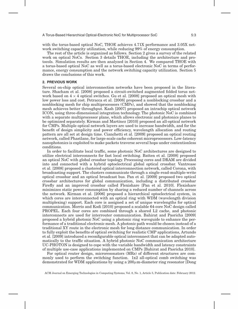
Fig. 7. Performance comparison for different MPSoC applications.
Fig. 8. Task completion time comparison for different MPSoC applications.
NoC and optical NoC. In addition, the task completion time of an application is anothermetric of system performance and efficiency. It is the latency from the beginning of theapplication until the corresponding end. Figure 8 shows the comparison of normalizedaverage task completion times under the same configuration. For an average of thesix applications, THOE reduces 26% of the task completion time compared with theoptical torus-based NoC, but has a slightly larger delay than the electronic one.
The high communication locality as well as the efficient hybrid switching mecha-nism contribute to the good performance of THOE. Each four processors are groupedtogether and traffic among them is handled by fast electronic switching. Another ad-vantage of the hierarchical architecture is smaller optical network diameter. For a256-core MPSoC, the global network size is reduced from 16 × 16 in the traditionaltorus-based optical NoC to 8 × 8 in THOE. It means that for the same communicationpeers, it takes fewer hops to arrive at the destination in THOE. In addition, as short-range communication traffic is offloaded by the hybrid optical-electronic routers, lessinterference is imposed to the fraction of long-range communication traffic. Networkcongestion has a big impact on the throughput and packet latency, so less networkcongestion helps improve the communication efficiency for intercluster traffic.
Figures 9 to 16 show the simulation results under uniform traffic, with packet sizeranging from 512B to 4096B. Network performance was evaluated and compared inmetrics of packet end-to-end (ETE) delay and network throughput. Packet ETE delayis the average time a packet takes to reach the destination, and network throughputis defined as the total data transfer rate in the network under a given injection rate.The injection rate is defined as Equation (7), where Ttransmit is the time to transmit thepacket and Tinterval is the average time interval between the generation of two succes-sive packets. Tinterval follows a negative exponential distribution. For example, if theinjection rate is 0.5, the average time interval between the generation of two succes-sive packets is equal to the time of one packet transmission. The initial 100000 clock
ACM Journal on Emerging Technologies in Computing Systems, Vol. 8, No. 1, Article 5, Publication date: February 2012.

5:14 Y. Ye et al.
Fig. 9. Network throughput with 512B packets.
Fig. 10. Average ETE delay of 512B packets.
cycles of each simulation are run as the warm-up period to allow transient effects tostabilize.
α =Ttransmit
Ttransmit + Tinterval. (7)
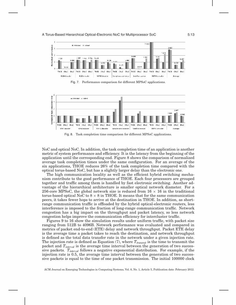
The overall performance trend of all six NoCs is similar. The network throughputincreases with the injection rate, and after a saturation point, the throughput stopsincreasing. It can be concluded from the figures that THOEs have better throughputthan the optical torus-based NoC, but worse than the electronic folded torus. For 512Bpackets, the electronic torus-based NoCs saturate at an injection rate of about 0.15,with saturation throughputs of 1085Gbps and 1375Gbps respectively for the unfoldedand folded scenarios. THOEs saturate at an earlier injection rate with saturationthroughputs of about 920Gbps and 840Gbps respectively for the unfolded and foldedscenarios. It can also be observed that NoC performance is affected by the packetsize. For optical NoCs with circuit switching, larger packet size corresponds to lesselectronic control overhead and thus leads to better performance. For 4096B pack-ets, saturation throughputs of the unfolded and folded THOEs are about 1135Gbpsand 1085Gbps respectively, higher than the throughputs with 512B packets. Some
ACM Journal on Emerging Technologies in Computing Systems, Vol. 8, No. 1, Article 5, Publication date: February 2012.

A Torus-Based Hierarchical Optical-Electronic NoC for Multiprocessor SoC 5:15
Fig. 11. Network throughput with 1024B packets.
Fig. 12. Average ETE delay of 1024B packets.
of the packets in THOE are delivered through local electronic switching, but for thetorus-based optical NoC, all the packets are transmitted in the optical domain. Sopacket size has a bigger impact on the network throughput for the torus-based opticalNoC. The optical torus-based NoCs saturate at about 600Gbps for 512B packets, andthe saturation throughputs increase to more than 1100Gbps for 4096B packets. Onthe other hand, electronic packet switching is more efficient for small packets, so thethroughput of the electronic torus-based NoCs decreases when using a larger packetsize. For 4096B packets, the electronic folded torus still has the best throughput, butthe unfolded one has less throughput than both THOEs and the optical torus-basedNoCs. Regarding packet ETE delay, before network saturation, the average delay ofTHOEs is better than the electronic unfolded torus and the optical torus-based NoCs.For 512B packets, when the injection rate is 0.03, the average ETE delays in THOEsand optical torus-based NoCs are about 0.166μs and 0.231μs respectively. The elec-tronic folded torus-based NoC has better latency, which is 0.146μs. For 4096B packets,when the injection rate is 0.03, the average ETE delays in THOEs and optical torus-based NoCs are about 1.120μs. The electronic folded torus-based NoC has an average
ACM Journal on Emerging Technologies in Computing Systems, Vol. 8, No. 1, Article 5, Publication date: February 2012.

5:16 Y. Ye et al.
Fig. 13. Network throughput with 2048B packets.
Fig. 14. Average ETE delay of 2048B packets.
latency of 0.969μs, which outperforms other NoCs. The better performance of the elec-tronic folded torus NoC under uniform traffic (which is unrealistic) shows that theelectronic torus-based NoC has more network resources. But for real MPSoC appli-cations, only a small part of the network resources can be used and THOE achieves2.46X performance compared with the electronic torus-based NoC.
4.2. Energy Consumption Comparison
We evaluated the energy efficiency of the 256-core THOE, and compared it with thetorus-based optical NoC as well as the electronic one for the six MPSoC applicationsand a uniform traffic pattern.
NoC energy efficiency is measured as the average energy consumption per bit fortransferring packets in the network. For an intracluster packet in THOE, energy con-sumption includes the energy required to transfer the packet through the two localelectrical interconnects, the energy dissipated by the local electronic switching fab-ric, and the energy consumed by the control unit. For an intercluster packet, energyconsumption involves the energy consumed by the control packets in the electronic
ACM Journal on Emerging Technologies in Computing Systems, Vol. 8, No. 1, Article 5, Publication date: February 2012.
A Torus-Based Hierarchical Optical-Electronic NoC for Multiprocessor SoC 5:17
Fig. 15. Network throughput with 4096B packets.
Fig. 16. Average ETE delay of 4096B packets.
control network and the energy consumed by the payload in the optical domain. Theenergy consumption for a control packet is estimated as the sum of the energy re-quired to transfer it through all the electrical interconnects and electronic switchingfabrics along the path, and the energy consumed by the control units in all of the in-termediate routers. The energy consumed by the payload includes the energy used fortransferring data through the two local electrical interconnects and through the elec-tronic switching fabrics in the source and destination processors, the energy consumedby O/E interfaces, and MR energy consumption in the optical path.
A typical O/E interface includes serializer, driver, VCSEL, waveguide, photodetec-tor, TIA-LA circuits, and deserializer. Energy consumption for EO and OE conversionsin an optical link is the sum of the power consumed by all components of the O/Einterface. O/E interface power efficiency has a direct impact on the energy consump-tion of optical NoCs. Optical energy would decrease linearly by improving O/E inter-face power efficiency. With certain device technologies, power dissipated in an opticaltransceiver is mainly governed by the laser source. We assume that the VCSELs are di-rectly modulated by driving currents and no external modulation is needed during op-tical transmission. The necessary optical power emission generated at the source Psrc
ACM Journal on Emerging Technologies in Computing Systems, Vol. 8, No. 1, Article 5, Publication date: February 2012.

5:18 Y. Ye et al.
Fig. 17. The impact of optical loss on O/E power efficiency.
Table I. Power Efficiency of O/E Interface in THOE
O/E interface component Power efficiency in 45nm (pJ/bit)
VCSEL driver 0.1125VCSEL 0.478
Photodetector 0.0003
TIA-LA circuits 0.3375Serializer/deserializer 0.288
can be estimated as the sum of optical power loss in the path and the minimum opticalpower required at the destination (Equation (5)). The output power of the source VC-SEL should be no less than Psrc. With a driving current of I, the output optical powerof VCSEL is as Equation (8), where S is the slope efficiency and Ith is the thresholdcurrent.
PVCSELout = S · (I − Ith). (8)
Based on the VCSEL model in Syrbu et al. [2008], we assume that if the drivingcurrent I is above the threshold current Ith of 2.5mA, output power will increase ap-proximately linearly with the driving current with slope efficiency S of 0.36mW/mA.VCSEL power consumption can be calculated as UI, where U is the bias voltage andis also assumed to increase linearly with the driving current I. The range of opticalpower loss decides VCSEL power consumption directly, and VCSEL power consump-tion would dominate the total O/E interface power consumption when loss is large. Byimproving the optical power loss in the THOE and implementing the adaptive powercontrol mechanism, the average VCSEL power consumption for the six MPSoC appli-cations is expected to be reduced.
In addition to improving device technologies of optical transceivers, O/E power effi-ciency can also be improved by reducing optical power loss encountered in the opticallink. Figure 17 shows that O/E power consumption stays at a relatively low level inthe low loss range, but increases exponentially when loss is large. Table I shows thepower consumption of the O/E interface in THOE. Here we use the serializer and de-serializer design in Poulton et al. [2007], and the VCSEL driver and TIA-LA designsin Kromer et al. [2005]. The power consumption of the VCSEL driver and TIA-LAcircuits is 0.82pJ/bit in 80-nm CMOS. The power consumption of the serializer and de-serializer is 0.576pJ/bit in 90-nm CMOS. Since the electronic part of THOE is in 45nm,
ACM Journal on Emerging Technologies in Computing Systems, Vol. 8, No. 1, Article 5, Publication date: February 2012.

A Torus-Based Hierarchical Optical-Electronic NoC for Multiprocessor SoC 5:19
Fig. 18. Energy efficiency comparison under different MPSoC applications.
Fig. 19. Energy efficiency comparison with uniform traffic.
we scale all the related power consumption linearly to 45nm. For example, the driverand TIA-LA circuits’ power consumption is scaled from 0.2pJ/bit and 0.6pJ/bit in 80nmto 0.1125pJ/bit and 0.3375pJ/bit in 45nm, and the power consumption of the serializerand deserializer is scaled from 0.576pJ/bit in 90nm to 0.288pJ/bit in 45nm. The pho-todetector model is based on a Ge waveguide photodetector monolithically integratedin a 130nm CMOS process with a sensitivity of −14.2dBm for 10−12 BER [Masini et al.2007]. Though the work in Zheng et al. [2010] reported a better receiver sensitivity of−18.9dBm for the same BER, it operates at a much lower data rate than Masini et al.[2007]. When the optical power loss in the path is 11dB, the VCSEL power consump-tion is about 0.478pJ/bit and the total power efficiency of the O/E interface is about1.22pJ/bit. With other similar device models, detailed values in Figure 17 could bechanged but the trend is the same.
Figures 18 and 19 compare the energy efficiency of THOE with the torus-based op-tical NoCs and electronic NoCs with different MPSoC applications and uniform trafficpattern. Electrical energy represents the portion of total energy consumed in the elec-tronic domain, and optical energy is the portion of total energy consumed in the opticaldomain. For optical NoCs, most energy is consumed in O/E interfaces and only a smallpart of the energy is cost for electronic control. The percentage of electrical energyincreases in THOE because local traffic is delivered through electronic switching, andonly intercluster packets consume energy in the optical domain. Figure 18 shows thatTHOE consumes less energy for all the applications. For the local electronic switching,we assume that the average energy required to transfer a single bit through a cross-bar is 0.07pJ/bit, the average energy dissipated in an electrical interconnect betweenprocessor and router is 0.04pJ/bit, and the average energy consumed by the buffer is0.003pJ/bit.
ACM Journal on Emerging Technologies in Computing Systems, Vol. 8, No. 1, Article 5, Publication date: February 2012.

5:20 Y. Ye et al.
Fig. 20. Average optical power loss distributions in THOE and optical torus-based NoC.
After including the VCSEL power consumption, the average power efficiency ofTHOE is 0.856pJ/bit for the H263 encoder application. It reduces about 89% of the av-erage power consumption as compared to the electronic torus-based NoC (8.175pJ/bit).The worst-case power consumption of optical transmission in THOE could be largerthan this. Since part of traffic is intracluster packet switching, which is power effi-cient, the average power consumption is lowered. On average of the six applications,THOE reduces 99% of energy compared to the optical NoC and 84% compared to theelectronic NoC. The portion of energy consumed in the electronic domain in THOE isabout 28.6%, including energy consumption for path control and intracluster packettransmission. The good power efficiency of THOE demonstrates that the whole archi-tecture and low-loss low-power techniques are well designed. For uniform traffic withpacket size ranging from 512B to 4096B, THOE consumes about 1.32pJ/bit on aver-age, which is only 11.9% of the energy consumption in the electronic torus-based NoC.Since the size of the control packets is relatively small as compared with the payload,the overhead of electronic control in THOE is not serious—the portion of energy con-sumption for electronic control is about 17.3% for uniform traffic. Due to the largeworst-case optical power loss encountered by packets, the optical torus-based NoC hasthe worst energy efficiency for the uniform traffic as well as several real applications.The maximum VCSEL output power is about 4mW (6dBm) [Syrbu et al. 2008], andthe photodetector sensitivity is -14.2dBm with 10−12 BER [Masini et al. 2007]. To en-sure that the optical signal reaching the photodetector is detectable, the optical signalpower received by the receiver should not be lower than the receiver sensitivity.
Optical power loss in a path can be estimated by adding the loss of each component.We assumed that the chip size is 10mm × 10mm. Detailed loss components wereestimated from current technologies. Waveguide propagation loss is about 0.17dB/mm;MR on-state drop-port loss is about 0.5dB; MR off-state through-port loss is about0.005dB; waveguide crossing insertion loss is about 0.12dB; waveguide bending lossis about 0.005dB [Lee et al. 2008; Poon et al. 2008; Xia et al. 2007; Xiao et al. 2007].Figure 20 shows the average packet distribution over different optical power lossranges for the six applications. Compared with the optical torus-based NoC, the opticalpower loss in THOE is significantly improved, and the worst-case loss is about 10.6dB.With the photodetector sensitivity of −14.2dBm, only 0.44mW laser power is neededat the transmitter side. Based on the VCSEL design in Syrbu et al. [2008], even athigh temperatures like 80oC, the maximum output power of 1.5mW is still enough for
ACM Journal on Emerging Technologies in Computing Systems, Vol. 8, No. 1, Article 5, Publication date: February 2012.

A Torus-Based Hierarchical Optical-Electronic NoC for Multiprocessor SoC 5:21
Table II. Optical Resources Cost for a 256-core MPSoC Using Different Communication Architectures
THOE Typical torus-based ONoC
The torus network[Shacham et al. 2008]
Corona[Vantrease et al. 2008]
Optical router 64 256 1K /Laser source 64 256 256 /Photodetector 128 256 256 20K
Microresonator 896 4K 8K 1032KOptical terminator 192 2.5K / /
Waveguide crossing 176 1352 4.25K /
the worst-case emission power required of THOE. In the optical torus-based NoC, theworst-case loss is much worse: about 44.6dB.
The significant loss reduction is due to the high communication locality, the smalleroptical network diameter, as well as the low-loss techniques employed in THOE, suchas floorplan optimization and the low-loss optical switching fabric, Crux. In both theunfolded and folded THOEs, on average for the six MPSoC applications, about 57.8%of packets have 0dB optical power loss, which means that about half of the packetsbelong to intracluster traffic. Such a high proportion of intracluster traffic shows thehigh communication locality achieved in THOE for real MPSoC applications. In addi-tion, just as mentioned before, it takes fewer hops to arrive at the destination in THOEfor the same communication peers. The smaller number of hops ensures that opticalsignals encounter less optical power loss. Besides, the efforts of floorplan optimizationand Crux are focused on loss reduction. Packets in THOEs suffer less power loss andthus require less power. In addition, since the loss of each path is different, the adap-tive power control mechanism plays an important role in further reducing the powerconsumption of THOE.
4.3. Network Resource Analysis
Table II compares the cost of optical resources for a 256-core MPSoC using differentcommunication architectures. Compared with the optical torus-based NoC, THOE re-duces 75% of optical switching fabrics and laser sources, meanwhile costs 50% lessthan electronic switching fabrics and photodetectors. As described in the preceding,THOE uses Crux instead of optimized crossbar in the reference optical NoC. Each Cruxoptical switching fabric reduces the number of MRs from 16 to 14, and reduces opticalterminators from ten to three. Thus for a 256-core MPSoC, THOE reduces 78% of MRsand 92% of optical terminators in total. For waveguide crossings, the comparison of thetotal number of crossings in the network level is shown in the table. Here we assumethe optical links are all bidirectional and that there are two waveguides for each linkbetween routers. Compared with the torus-based optical NoC, THOE reduces waveg-uide crossings from 1296 to 96 in the unfolded scenario and from 1408 to 256 in thefolded scenario. On average, THOE has 176 waveguide crossings and the torus-basedoptical NoC has 1352 crossings at the network level. About 87% of waveguide cross-ings are reduced. The floorplan optimization technology and the smaller diameter ofthe optical network both contribute to the significant reduction of waveguide crossings.
We also show the cost comparison with the folded torus network proposed inShacham et al. [2008] and Corona [Vantrease et al. 2008]. To interconnect MxNcores (when both M and N are even), the folded torus network [Shacham et al. 2008]needs 4MN 4 × 4 optical switches in total, including MN gateway switches, MNinjection switches, MN ejection switches, and MN optical routers. Correspondingly,THOE only needs MN
4 5 × 5 optical switching fabrics, which also results in muchfewer MRs. Corona [Vantrease et al. 2008] is chosen as a representative example of
ACM Journal on Emerging Technologies in Computing Systems, Vol. 8, No. 1, Article 5, Publication date: February 2012.

5:22 Y. Ye et al.
Fig. 21. Network switching capacity utilization comparison for different MPSoC applications.
Fig. 22. Network switching capacity utilization comparison for uniform traffic.
optical crossbars. There is a tradeoff between cost and performance for each work,and optical crossbar’s performance advantages are due to the large network resources.For example, for a 256-core system, the total number of microresonators in THOEis 896, while Shacham et al. [2008] uses 8K and Corona needs 1032K. THOE onlyneeds 10.9% of the microresonators used by Shacham et al. [2008] and 0.085% of themicroresonators used by Corona.
Waveguide can be fabricated on a silicon-on-insulator (SOI) wafer with a silicondevice slab on top of a buried oxide (BOX) layer, which prevents the optical mode fromleaking to the substrate. The cross-section of a single-mode waveguide was designed tomeasure 510 × 226 nm with minimum propagation loss and group velocity dispersion[Xia et al. 2007]. The area of a single Crux optical switching fabric is about 4430μm2,with 10μm-diameter MRs. For a 256-core MPSoC with chip size of 10mm × 10mm2,the total area of waveguide and optical switching fabrics is about 1.22mm2 in unfoldedTHOE and 1.13mm2 in the folded one. For the electronic control network of THOE,the total silicon area is about 1.73mm2 in 45nm technology, and the total metal area isabout 12.39mm2.
Figures 21 and 22 show the comparison for network switching capacity utilizationfor real MPSoC applications as well as uniform traffic. The network switching capacityutilization is defined as Equation (9), where Sused is the amount of switching capacityused, and Stotal is the total amount of switching capacity available in the network. ForTHOE and optical torus-based NoC, Stotal includes the switching capacity of the data-transmission network as well as the electronic control network. Because of the hierar-chical architecture, the total switching capacity available in THOE is only about half ofthe reference optical torus-based NoC as well as the electronic NoC. On average for the
ACM Journal on Emerging Technologies in Computing Systems, Vol. 8, No. 1, Article 5, Publication date: February 2012.

A Torus-Based Hierarchical Optical-Electronic NoC for Multiprocessor SoC 5:23
six MPSoC applications, THOE achieves about 1.51X and 3.05X utilization comparedwith the torus-based electronic NoC and optical NoC respectively. For uniform traffic,the utilization increases with the injection rate until network saturation. On averageof the unfolded and folded scenarios, THOE achieves about 23% utilization when thenetwork is saturated, while 19% and 11% utilization are achieved respectively in thetorus-based electronic NoC and the optical one.
Utilization =Sused
Stotal. (9)
5. CONCLUSION
We propose a torus-based hierarchical hybrid optical-electronic NoC, called THOE,for exploration of high communication efficiency. Four new techniques are employedto further improve the power efficiency, including floorplan optimization, adaptivepower control mechanism, low-latency control protocols, and low-power opticalswitching fabric. We compared THOE with torus-based electronic NoC and opticalNoC for a 256-core MPSoC using real MPSoC applications. On average for the setof real applications, compared with the electronic torus-based NoC, THOE achieves2.46X performance with 84% reduction of energy consumption. Compared with thetorus-based optical NoC, THOE achieves 4.71X performance while reducing 99%of energy consumption. For the network switching capacity, it achieves 1.51X and3.05X utilization respectively compared with the reference torus-based electronic NoCand optical NoC. Besides real applications, we also used uniform traffic patterns toanalyze the average packet delay and network throughput of THOE. As for networkresources, THOE reduces 75% of lasers and uses half the photodetectors comparedwith the torus-based optical NoC.
ACKNOWLEDGMENTS
The authors are grateful to the reviewers who offered us helpful suggestions to improve this work.
REFERENCESANAN, T., SUZUKI, N., YASHIKI, K., FUKATSU, K., HATAKEYAMA, H., AKAGAWA, T., TOKUTOME, K.,
AND TSUJI, M. 2008. High-speed 1.1-um-range InGaAs VCSELs. In Proceedings of the Optical FiberCommunication/National Fiber Optic Engineers Conference. 1–3.
ARTUNDO, I., HEIRMAN, W., LOPERENA, M., DEBAES, C., VAN CAMPENHOUT, J., AND THIENPONT, H.2009. Low-power reconfigurable network architecture for on-chip photonic interconnects. In Proceedingsof the 17th IEEE Symposium on High Performance Interconnects (HOTI). 163–169.
BAHIRAT, S. AND PASRICHA, S. 2009. Exploring hybrid photonic networks-on-chip foremerging chip multi-processors. In Proceedings of the 7th IEEE/ACM International Conference on Hardware/Software Code-sign and System Synthesis (CODES+ISSS). 129–136.
BAHIRAT, S. AND PASRICHA, S. 2010. UC-PHOTON: A novel hybrid photonic network-on-chip for multipleuse-case applications. In Proceedings of the 11th International Symposium on Quality Electronic Design(ISQED). 721–729.
BALFOUR, J. AND DALLY, W. J. 2006. Design tradeoffs for tiled CMP on-chip networks. In Proceedings ofthe 20th Annual International Conference on Supercomputing (ICS). 187–198.
BATTEN, C., JOSH, A., ORCUTT, J., KHILO, A., MOSS, B., HOLZWARTH, C., POPOVIC, M., LI, H., SMITH,H., HOYT, J., KARTNER, F., RAM, R., STOJANOVIC, V., AND ASANOVIC, K. 2008. Building manycoreprocessor-to-DRAM networks with monolithic silicon photonics. In Proceedings of the 16th IEEE Sym-posium on High Performance Interconnects (HOTI). 21–30.
BENINI, L. AND DE MICHELI, G. 2001. Powering networks on chips. In Proceedings of 14th InternationalSymposium on System Synthesis (ISSS). 33–38.
BENINI, L. AND DE MICHELI, G. 2002. Networks on chip: A new paradigm for systems on chip design. InProceedings of the Design, Automation and Test in Europe Conference and Exhibition (DATE). 418–419.
ACM Journal on Emerging Technologies in Computing Systems, Vol. 8, No. 1, Article 5, Publication date: February 2012.

5:24 Y. Ye et al.
BIBERMAN, A., LEE, B., SHERWOOD-DROZ, N., LIPSON, M., AND BERGMAN, K. 2010. Broadband operationof nanophotonic router for silicon photonic networks-on-chip. IEEE Photon. Technol. Lett. PP 99, 1–1.
BJERREGAARD, T. AND MAHADEVAN, S. 2006. A survey of research and practices of network-on-chip. ACMComput. Surv. 38, 1, 1.
BONETTO, E., CHIARAVIGLIO, L., CUDA, D., GAVILANES CASTILLO, G., AND NERI, F. 2009. Optical tech-nologies can improve the energy efficiency of networks. In Proceedings of the 35th European Conferenceon Optical Communication (ECOC). 1–4.
BRIERE, M., GIRODIAS, B., BOUCHEBABA, Y., NICOLESCU, G., MIEYEVILLE, F., GAFFIOT, F., ANDO’CONNOR, I. 2007. System level assessment of an optical NoC in an MPSoC platform. In Proceed-ings of the Design, Automation and Test in Europe Conference and Exhibition (DATE). 1–6.
CHEN, G., CHEN, H., HAURYLAU, M., NELSON, N. A., ALBONESI, D. H., FAUCHET, P. M., AND FRIEDMAN,E. G. 2007. Predictions of CMOS compatible on-chip optical interconnect. VLSI J. Integration 40, 4,434–446.
CHEN, X., MOHAMED, M., SCHWARTZ, B., LI, Z., SHANG, L., AND MICKELSON, A. 2010. Racetrack filtersfor nanophotonic on-chip networks. In Proceedings of the Conference on Integrated Photonics Research,Silicon and Nanophotonics (ITPR).
CHO, H., KAPUR, P., AND SARASWAT, K. 2004. Power comparison between high-speed electrical and opti-cal interconnects for inter-chip communication. In Proceedings of the IEEE International InterconnectTechnology Conference (IITC). 116–118.
CIANCHETTI, M. J., KEREKES, J. C., AND ALBONESI, D. H. 2009. Phastlane: A rapid transit optical routingnetwork. In Proceedings of the 36th Annual International Symposium Computer Architecture (ISCA).441–450.
DALLY, W. AND SEITZ, C. 1987. Deadlock-free message routing in multiprocessor interconnection networks.IEEE Trans. Comput. C-36 5, 547–553.
DALLY, W. AND TOWLES, B. 2001. Route packets, not wires: On-chip interconnection networks. In Proceed-ings of the Design Automation Conference (DAC). 684–689.
DAS, R., EACHEMPATI, S., MISHRA, A., NARAYANAN, V., AND DAS, C. 2009. Design and evaluation of ahierarchical on-chip interconnect for next-generation CMPs. In Proceedings of the IEEE 15th Interna-tional Symposium on High Performance Computer Architecture (HPCA). 175–186.
DONG, P., PREBLE, S. F., AND LIPSON, M. 2007. All-optical compact silicon comb switch. Opt. Express 15,15, 9600–9605.
DOYLEND, J. AND KNIGHTS, A. 2006. Design and simulation of an integrated fiber-to-chip coupler forsilicon-on-insulator waveguides. IEEE J. Sel. Topics Quantum Electron. 12, 6, 1363–1370.
GU, H., XU, J., AND WANG, Z. 2008. A novel optical mesh network-on-chip for gigascale systems-on-chip. InProceedings of the IEEE Asia Pacific Conference on Circuits and Systems (APCCAS). 1728–1731.
GU, H., MO, K. H., XU, J., AND ZHANG, W. 2009. A low-power low-cost optical router for optical networks-on-chip in multiprocessor systems-on-chip. In Proceedings of the IEEE Computer Society Annual Sym-posium on VLSI (ISVLSI). 19–24.
HU, J. AND MARCULESCU, R. 2003. Energy-aware mapping for tile-based NOC architectures under per-formance constraints. In Proceedings of the Asia and South Pacific Design Automation Conference(ASP DAC). 233–239.
HU, J., OGRAS, U. Y., AND MARCULESCU, R. 2006. System-level buffer allocation for application-specificnetworks-on-chip router design. IEEE Trans. Computer-Aided Design Integr. Circuits Syst. 25, 12,2919–2933.
JI, C., WANG, J., SODERSTROM, D., AND GIOVANE, L. 2009. High data rate 850 nm oxide VCSEL for20 Gb/s application and beyond. In Proceedings of the Communications and Photonics Conference andExhibition, Asia (ACP). 1–2.
KASH, J. 2007. Intrachip optical networks for a future supercomputer-on-a-chip. In Proceedings of Photonicsin Switching (PS). 55–56.
KIRMAN, N., KIRMAN, M., DOKANIA, R., MARTINEZ, J., APSEL, A., WATKINS, M., AND ALBONESI, D.2006. Leveraging optical technology in future bus-based chip multiprocessors. In Proceedings of the39th Annual IEEE/ACM International Symposium on Microarchitecture (MICRO). 492–503.
KIRMAN, N. AND MARTINEZ, J. F. 2010. A power-efficient all-optical on-chip interconnect using wavelength-based oblivious routing. In Proceedings of the 15th Annual International Conference on ArchitecturalSupport for Programming Languages and Operating Systems (ASPLOS). 15–28.
KROMER, C., SIALM, G., BERGER, C., MORF, T., SCHMATZ, M., ELLINGER, F., ERNI, D., BONA, G.-L.,AND JACKEL, H. 2005. A 100-mW 4 x 10 Gb/s transceiver in 80-nm CMOS for high-density opticalinterconnects. IEEE J. Solid-State Circuits 40, 12, 2667–2679.
ACM Journal on Emerging Technologies in Computing Systems, Vol. 8, No. 1, Article 5, Publication date: February 2012.

A Torus-Based Hierarchical Optical-Electronic NoC for Multiprocessor SoC 5:25
KUMAR, S., JANTSCH, A., SOININEN, J.-P., FORSELL, M., MILLBERG, M., OBERG, J., TIENSYRJA, K., ANDHEMANI, A. 2002. A network on chip architecture and design methodology. In Proceedings of the IEEEComputer Society Annual Symposium on VLSI (ISVLSI). 105–112.
LEE, H. G., CHANG, N., OGRAS, U. Y., AND MARCULESCU, R. 2007. On-chip communication architectureexploration: A quantitative evaluation of point-to-point, bus, and network-on-chip approaches. ACMTrans. Des. Autom. Electron. Syst. 12, 3, 1–20.
LEE, B., BIBERMAN, A., DONG, P., LIPSON, M., AND BERGMAN, K. 2008. All-optical comb switch for multi-wavelength message routing in silicon photonic networks. IEEE Photon. Technol. Lett. 20, 10, 767–769.
LIU, W., YUAN, M., HE, X., GU, Z., AND LIU, X. 2008. Efficient SAT-Based mapping and scheduling ofhomogeneous synchronous dataflow graphs for throughput optimization. In Proceedings of the Real-Time Systems Symposium (RTSS). 92–504.
LOTT, J. A., LEDENTSOV, N. N., SHCHUKIN, V. A., MUTIG, A., BLOKHIN, S. A., NADTOCHIY, A. M., FIOL,G., AND BIMBERG, D. 2010. 850 nm VCSELs for up to 40 Gbit/s short reach data links. In Proceedingsof the Conference on Lasers and Electro-Optics (CLEO) and Quantum Electronics and Laser ScienceConference (QELS). 1–2.
MAJER, M., BOBDA, C., AHMADINIA, A., AND TEICH, J. 2005. Packet routing in dynamically changingnetworks on chip. In Proceedings of the 19th IEEE International Symposium on Parallel and DistributedProcessing (PDPTA).
MASINI, G., CAPELLINI, G., WITZENS, J., AND GUNN, C. 2007. A 1550nm, 10Gbps monolithic optical re-ceiver in 130nm CMOS with integrated Ge waveguide photodetector. In Proceedings of the 4th IEEEInternational Conference Group IV Photonics (GFP). 1–3.
MICHELOGIANNAKIS, G., PNEVMATIKATOS, D., AND KATEVENIS, M. 2007. Approaching ideal NOC latencywith pre-configured routes. In Proceedings of the 1st International Symposium of Networks-on-Chip(NOCS). 153–162.
MORRIS, R. AND KODI, A. K. 2010. Exploring the design of 64- and 256-core power efficient nanophotonicinterconnect. IEEE J. Sel. Topics Quantum Electron. PP, 99, 1–8.
NI, L. AND MCKINLEY, P. 1993. A survey of wormhole routing techniques in direct networks. Comput. 26,2, 62–76.
O’CONNOR, I. 2004. Optical solutions for system-level interconnect. In Proceedings of the InternationalWorkshop on System Level Interconnect Prediction (SLIP). 79–88.
O’CONNOR, I., TISSAFI-DRISSI, F., NAVARRO, D., MIEYEVILLE, F., GAFFIOT, F., DAMBRE, J., DE WILDE,M., STROOBANDT, D., AND BRIERE, M. 2006. Integrated optical interconnect for on-chip data transport.In Proceedings of the IEEE North-East Workshop on Circuits and Systems (NEWCAS). 209–209.
PAN, Y., KIM, J., AND MEMIK, G. 2010. Flexishare: Channel sharing for an energy-efficient nanophotoniccrossbar. In Proceedings of the IEEE 16th International Symposium on High Performance ComputerArchitecture (HPCA). 1–12.
PAN, Y., KUMAR, P., KIM, J., MEMIK, G., ZHANG, Y., AND CHOUDHARY, A. 2009. Firefly: Illuminatingfuture network-on-chip with nanophotonics. In Proceedings of the 36th International Symposium onComputer Architecture (ISCA).
PANDE, P. P., GRECU, C., JONES, M., IVANOV, A., AND SALEH, R. 2005. Performance evaluation and designtrade-offs for network-on-chip interconnect architectures. IEEE Trans. Comput. 54, 8, 1025–1040.
PASRICHA, S. AND DUTT, N. 2008. Trends in emerging on-chip interconnect technologies. Inform. MediaTechnol. 3, 4, 630–645.
PERKINS, J. AND FONSTAD, C. 2007. Low threshold VCSELs recess-integrated on Si-CMOS ICs. In Pro-ceedings of the Conference on Lasers and Electro-Optics (CLEO). 1–2.
PERKINS, J. M., SIMPKINS, T. L., WARDE, C., AND CLIFTON G. FONSTAD, J. 2008. Full recess integrationof small diameter low threshold VCSELs within Si-CMOS ICs. Opt. Express 16, 18, 13955–13960.
PETRACCA, M., LEE, B., BERGMAN, K., AND CARLONI, L. 2008. Design exploration of optical interconnec-tion networks for chip multiprocessors. In Proceedings of the 16th IEEE Symposium High PerformanceInterconnects (HOTI). 31–40.
POON, A. W., XU, F., AND LUO, X. 2008. Cascaded active silicon microresonator array cross-connect circuitsfor WDM networks-on-chip. Silicon Photonics III 6898, 1.
POULTON, J., PALMER, R., FULLER, A., GREER, T., EYLES, J., DALLY, W., AND HOROWITZ, M. 2007. A14-mW 6.25-Gb/s transceiver in 90-nm CMOS. IEEE J. Solid-State Circuits 42, 12, 2745–2757.
RIJPKEMA, E., GOOSSENS, K., RADULESCU, A., DIELISSEN, J., VAN MEERBERGEN, J., WIELAGE, P., ANDWATERLANDER, E. 2003. Trade-offs in the design of a router with both guaranteed and best-effortservices for networks on chip. In Proceedings of the Conference on Design, Automation and Test in Europe(DATE).
ACM Journal on Emerging Technologies in Computing Systems, Vol. 8, No. 1, Article 5, Publication date: February 2012.

5:26 Y. Ye et al.
SHACHAM, A., BERGMAN, K., AND CARLONI, L. 2008. Photonic networks-on-chip for future generations ofchip multiprocessors. IEEE Trans. Comput. 57, 9, 1246–1260.
SYRBU, A., MEREUTA, A., IAKOVLEV, V., CALIMAN, A., ROYO, P., AND KAPON, E. 2008. 10 Gbps VCSELswith high single mode output in 1310nm and 1550 nm wavelength bands. In Proceedings of the Confer-ence on Optical Fiber Communication/National Fiber Optic Engineers (OFC/NFOEC). 1–3.
VANTREASE, D., SCHREIBER, R., MONCHIERO, M., MCLAREN, M., JOUPPI, N., FIORENTINO, M., DAVIS,A., BINKERT, N., BEAUSOLEIL, R., AND AHN, J. 2008. Corona: System implications of emergingnanophotonic technology. In Proceedings of the 35th International Symposium on Computer Architec-ture (ISCA). 153–164.
VLASOV, Y., GREEN, W. M. J., AND XIA, F. 2008. High-throughput silicon nanophotonic wavelength-insensitive switch for on-chip optical networks. Nature Photonics 2, 242–246.
XIA, F. A., SEKARIC, L. A., AND VLASOV, Y. T. 2007. Ultracompact optical buffers on a silicon chip. NaturePhotonics 1, 65–71.
XIAO, S., KHAN, M. H., SHEN, H., AND QI, M. 2007. Multiple-channel silicon micro-resonator based filtersfor WDM applications. Opt. Express 15, 12, 7489–7498.
XU, J., WOLF, W., HENKEL, J., AND CHAKRADHAR, S. 2005. 264 HDTV decoder using application-specific networks-on-chip. In Proceedings of the IEEE International Conference on Multimedia and Expo(ICME). 1508–1511.
YIN, T., COHEN, R., MORSE, M. M., SARID, G., CHETRIT, Y., RUBIN, D., AND PANICCIA, M. J. 2007. 31 GHzGe N-I-P waveguide photodetectors on silicon-on-insulator substrate. Opt. Express 15, 21, 13965–13971.
YOUNG, I., MOHAMMED, E., LIAO, J., KERN, A., PALERMO, S., BLOCK, B., RESHOTKO, M., AND CHANG, P.2009. Optical I/O technology for tera-scale computing. In Proceedings of the IEEE International Solid-State Circuits Conference (ISSCC). 468–469.
ZHENG, X., LIU, F., PATIL, D., THACKER, H., LUO, Y., PINGUET, T., MEKIS, A., YAO, J., LI, G., SHI,J., RAJ, K., LEXAU, J., ALON, E., HO, R., CUNNINGHAM, J. E., AND KRISHNAMOORTHY, A. V. 2010.A sub-picojoule-per-bit CMOS photonic receiver for densely integrated systems. Opt. Express 18, 1,204–211.
Received October 2010; revised January 2011, May 2011; accepted July 2011
ACM Journal on Emerging Technologies in Computing Systems, Vol. 8, No. 1, Article 5, Publication date: February 2012.


![Concurrence of Torus Mandibularis with Multiple Buccal ... · A torus is a dense cortical bone exostosis wrapped in poorly vascularized mucosa [1]. In the oral cavity, torus mandibularis](https://img.pdfslide.us/doc/110x75/5c8e80bc09d3f2d9168cbf64/concurrence-of-torus-mandibularis-with-multiple-buccal-a-torus-is-a-dense.jpg)


![A Torus-Based Hierarchical Optical-Electronic Network-on ...mnikdast/files/papers/Mahdi_J3.pdfKirman and Mart´ınez [2010] proposed an all-optical network for CMPs. Multiple optical](https://img.pdfslide.us/doc/110x75/60c149f6a7f61176065e083a/a-torus-based-hierarchical-optical-electronic-network-on-mnikdastfilespapersmahdij3pdf.jpg)