Embed Size (px)
Citation preview
746 IEEE TI3.4NSACTIONS ON ELECTRON DEVICES, VOL. ED-24, NO. 6, JUNE 1977
[lo] D. Frohman-Bentchkowsky and A. S. Grove, “Conductance of MOSi transistors in saturation,” ZEEE Trans. Electron Deuices, vol ED-16, pp. 108-113, Jan. 1969.
[ll] R. Cobbold, Theory and Applications of Field-Effect Transistors New York Wiley-Interscience, 1970.
[12] H. C. Poon, L. D. Yau, R. L. Johnston, and D. Beecham, “DC mode for short-channel IGFET’s,” ZEDM 1973, pp. 156-159.
1131 S. Margalit, A. Neugroschel, and A. Bar-Lev, “Redistribution o ’
boron and phosphorus in silicon after two oxidation steps used in MOST fabrication,” ZEEE Trans. Electron Devices, vol. ED-19, pp. 861-868, July 1972.
[14] J. E. Meyer, “MOS models and circuit simulation,” RCA Reu., vol. 32, pp. 42-63, Mar. 1971.
[15] R. J. Van Overstraeten, G. J. Declerck, and P. A. Muls, “Theory of the MOS transistor in weak inversion,” ZEEE Trans. Electron Devices, vol. ED-22, pp. 282-288, May 1975.
A Symmetrically Balanced Linear Differential Charge-Splitting Input for Charger-Coupled Devices
Abstract-A new charge input scheme for charge-coupled dl:,- vices is described. Charge packets of a fixed size are produced i n , each clock cycle. Each charge packet is subsequently split into twa’ parts under two input gates. The difference between the two rd!.,. sulting fractional charge packets is a linear function of the ~I~II-,
tential difference between the two signal input gates. This input, scheme is particularly suitable for use with differential chargl!,,. coupled delay lines, since the charge representation of the ingrlit signal and its complement are produced in a highly symmetriotll manner. The principle may also be used for splitting charge packe tr, in any required ratio for more general application.
I. INTRODUCTION
A LARGE NUMBER of signal input schemes jf’jr charge-transfer devices have been described in tile
last few years. All these inputs are differential in princir:le since the input signal voltage is always compared to sor~le reference potential. In the current input method [l] or i n the voltage input scheme [a] it is the potential differen.:e between the input diode and the first or second input gti;e, respectively, that controls the amount of charge injectctl. In the charge preset or potential equilibration method [ 3 ] - [ 5 ] and its many variations [6], [7], the amount of charge inserted into the transfer channel is given by .the potential difference on two subsequent electrodes; and in a special implementation, designed to reduce effects of threshold voltage nosuniformities, the potential differeiwe representing the input signal and a reference voltage ;ire subsequently applied to one and the same electrode [ti].
Although these input schemes have brought abcullt successive improvements in linearity and dynamic rarge
Manuscript received July 30,1976; revised November 30,1976.
Computer Science, University of California, Berkeley, CA 94720 on leave C. H. Sequin is with the Department of Electrical Engineering ,lnd
from Bell Laboratories, Murray Hill, NJ 07974.
oratories, Murray Hill, NJ 07974. M. F. Tompsett, D. A. Sealer, and R. E. Crochiere are with Bell ][,ab-
[6], [9], they have only rarely been used in a truly differ- ential manner [lo], since often their common mode rejec- tion is rather poor. Furthermore, in most cases there is an inherent asymmetry in the function of the two electrodes that forces a one-sided relationship of the form Vreference > Vsignal or Vreference < Vsignal upon the two electrode po- tentials. This may necessitate special tricks to shift the dc level of one of the two signals. This was the case in a dif- ferential use of the charge preset input method to measure the voltage difference between the sense electrodes of a charge-coupled transversal split-electrode filter [lo].
For differential applications employing two charge- transfer channels carrying complementary signals [ll], [12], a more symmetrical input structure that produces balanced complementary charge packets even for a sin- gle-sided input signal appears highly desirable. Such an input scheme, which provides a symmetrically balanced differential input with good linearity and a clean saturation behavior, will now be described.
11. PESCRIPTION OF T H E NEW INPUT STRUCTURE
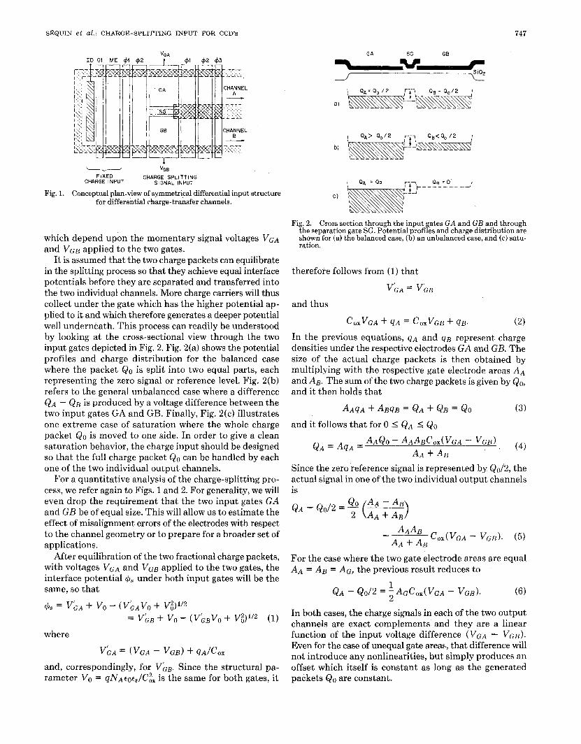
The basic idea behind the new input structure is to generate charge packets of a fixed size and to split them subsequently under the control of two input gates, so that the difference between the two fractional packets is a linear function of the voltage difference applied to the two input gates. Fig. 1 is a conceptual plan-view of the new input structure. It shows a charge input, consisting of input diode- (ID), gate 1 (Gl ) , and metering electrode (ME), which can be operated either in the voltage input or in the charge preset mode to produce charge packets of a fixed size Qo in each clock cycle. These charge packets are subsequently transferred to the actual signal input consisting of the two gates GA and GB, where each arriving charge packet Qo is split into two packets of sizes QA and QB, respectively,
SRQUIN et d.: CHARGE-SPLITTING INPUT FOR CCDs 747
VGA
L- VGB
CHARGE FIXED ,NPUT CHARGE SPLITTING SIGNAL INPUT
Fig. 1. Conceptual plan-view of symmetrical differential input structure for differential charge-transfer channels.
which depend upon the momentary signal voltages VGA and VCB applied to the two gates.
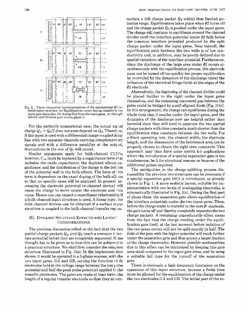
It is assumed that the two charge packets can equilibrate in the splitting process so that they achieve equal interface potentials before they are separated and transferred into the two individual channels. More charge carriers will thus collect under the gate which has the higher potential ap- plied to it and which therefore generates a deeper potential well underneath. This process can readily be understood by looking at the cross-sectional view through the two input gates depicted in Fig. 2. Fig. 2(a) shows the potential profiles and charge distribution for the balanced case where the packet Qo is split into two equal parts, each representing the zero signal or reference level. Fig. 2(b) refers to the general unbalanced case where a difference QA - QB is produced by a voltage difference between the two input gates GA and GB. Finally, Fig. 2(c) illustrates one extreme case of saturation where the whole charge packet Q o is moved to one side. In order to give a clean saturation behavior, the charge input should be designed SO that the full charge packet Qo can be handled by each one of the two individual output channels.
For a quantitative analysis of the charge-splitting pro- cess, we refer again to Figs. 1 and 2. For generality, we will even drop the requirement that the two input gates GA and GB be of equal size. This will allow us to estimate the effect of misalignment errors of the electrodes with respect to the channel geometry or to prepare for a broader set of applications.
After equilibration of the two fractional charge packets, with voltages VGA and VGB applied to the two gates, the interface potential $s under both input gates will be the same, so that
where
GA SG GB
Fig. 2. Cross section through the input gates GA and GB and through the separation gate SG. Potential profiles and charge distribution are shown for (a) the balanced case, (b) an unbalanced case, and (c) satu- ration.
therefore follows from (1) that
In the previous equations, q A and q B represent charge densities under the respective electrodes GA and GB. The size of the actual charge packets is then obtained by multiplying with the respective gate electrode areas A A and AB. The sum of the two charge packets is given by Qo, and it then holds that
AAQO - AAABCOX~VGA -- V G B ) AA + AB
QA = AqA . (4)
Since the zero reference signal is represented by Qo/2, the actual signal in one of the two individual output channels is
QA - Qo/2 = Q A A - A B 2 0 AA + AB
For the case where the two gate electrode areas are equal AA = AB = AG, the previous result reduces to
1 2 QA - Qo/2 = - A G C ~ , ( V G A - VGB). (6)
In both cases, the charge signals in each of the two output channels are exact complements and they are a linear function of the input voltage difference (VGA - V C R ) . Even for the case of unequal gate areas, that difference will not introduce any nonlinearities, but simply produces an offset which itself is constant as long as the generated _.
rameter vo-= qNAcots/Ck is-the same for both gates; it packets Qo are constant.
748 IEEE TRANSACTIONS ON ELECTRON DEVICES, JUNE 1977
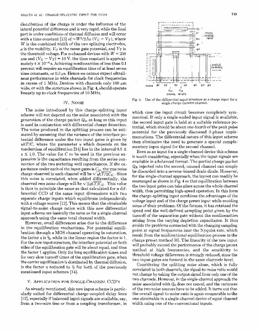
Fig. 3. Three conceptual implementations of the symmetrical d i f ! ’ ~ entia1 input structure. (a) Equilibration occurs during transfer to tlne input gate electrodes, (b) during flow from the input gates, (c) throi Ib:h special equilibration gate during phase 3.
For the perfectly symmetrical case, the actual sigzal charge QA - &0/2 does not even depend on Qo. Theref(. re, if this input is used with a differential charge-coupled delay line with two separate channels carrying complement iry signals and with a difference amplifier at the outl:ut, fluctuations in the size of Q o will cancel.
Similar arguments apply for bulk-channel CCll>’s; however, Cox must be replaced by a capacitance term .th.at includes the oxide capacitance, the depleted silicon ea- pacitance, and the distribution of the charge in the bot11 om of the potential well in the bulk silicon. The form of Ibis term is dependent on the exact doping of the bulk sili :on so that no specific cases will be analyzed. In general,, iin- creasing the electrode potential (n-channel device) will cause the charge to move nearer the electrode and ‘rice versa. Hence one can expect a superlinear re1ationsh.i p if a bulk-channel input structure is used. A linear inpull for bulk-channel devices can be obtained if a surface input structure is coupled to the bulk-channel transfer reg on.
111. DYNAMIC SPLITTING EFFECTS AND LA YOU^ CONSIDERATIONS
The previous discussion relied on the fact that the two partial charge packets QA and QB reach a common imter- face potential before they are completely separated. ‘3, ?me thought has to be given as to how this can be achieved in a practical structure. We shall first consider the siml;)I.est structure illustrated in Fig. 3(a). In the implement EI t ’ .ion shown, it would be operated in a 3-phase manner, with the two input gates, G A and GB, serving the function ( 14’ dc electrodes held in the voltage range between the low I.ulse potential and half the peak pulse potential applied t,lo the transfer electrodes. The gates are made at least twicr? the length of a regular transfer electrode so that they ac1l:om-
modate a full charge packet QO within that limited po- tential range. Equilibration takes place when 02 turns off and the charge packet QO is pushed under the input gates. The charge will continue to equilibrate around the channel divider until the interface potential under 02 falls below the common interface potential produced by the split charge packet under the input gates. Near turnoff, the equilibration path between the two wells is of low con- ductivity and, in addition, may be poorly defined due to spatial variations of the interface potential. Furthermore, since the discharge of the large area under 02 occurs si- multaneously with the equilibration process, this electrode must not be turned off too quickly lest proper equilibration be overruled by the dynamics of the discharge under the influence of the electrical fringe fields at the edges of the 02 electrode.
Alternatively, the beginning of the channel divider could be placed further to the right under the input gates themselves, and the remaining uncovered gap between the gates could be bridged by a self-aligned diode [Fig. 3(b)]. In this arrangement, the charge can equilibrate during the whole time that it resides under the input gates, and the dynamics of the discharge now are helpful rather than harmful since they will tend to separate the two partial charge packets with time constants much shorter than the equilibration time constants between the two wells. For a fixed operating rate, the channel width, the electrode length, and the dimensions of the bottleneck area can be properly chosen to obtain the right time constants:This approach may thus have some merits for applications where the introduction of a special separation gate is too cumbersome, be it for structural reasons or because of the additional pulses required.
The ambiguities in the charge-splitting process dis- cussed for the previous two structures can be overcome if a special separation gate (SG) is introduced, as already shown in Fig. 1. A more realistic layout, suitable for im- plementation with two levels of overlapping electrodes, is schematically illustrated in Fig. 3(c). During the first part of phase three, the separation gate allows equilibration of the interface potentials under the two input gates. Then, before the charge starts to transfer to the next 01 electrode, the gate turns off and thereby completely separates the two charge packets. A remaining unpredictable effect stems from the fact that the charge residing under the equili- bration gate itself, at the last moment before isolation of the two areas occurs will not be split exactly in half. The field of the gate with the higher potential will reach further under the separation gate and thus attract a larger fraction of the charge thereunder. However, possible nonlinearities due to this effect can be minimized by keeping this gate area small compared to the input gate areas, and by using a suitable fall time for the turnoff of the separation gate.
There is obviously a high-frequency limitation on the operation of this input structure, because a finite time must be allowed for the equilibration of the charge under the two electrodes GA and GB. The initial part of the re-
SeQUIN e t al.: CHARGE-SPLITTING INPUT FOR CCD's 749
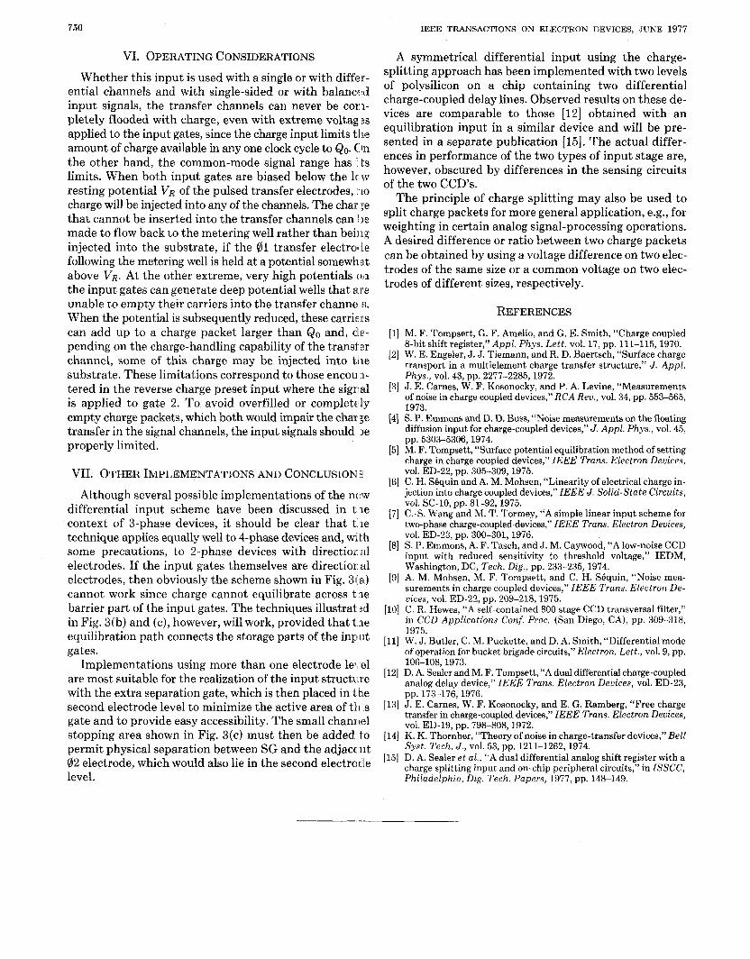
distribution of the charge is under the influence of the lateral potential difference and is very rapid, while the final part is under conditions of thermal diffusion and will occur with a time constant [13] of -W2/2.5g ( VG - V T ) , where W is the combined width of the two splitting electrodes, y is the mobility, VG is the mean gate potential, and VT is the threshold voltage. For n-channel devices with W = 250 ym and ( VG - V T ) = 10 V, the time constant is approxi- mately 4 X s. Achieving nonlinearities of less than 0.1 percent will require an equilibration time of at least seven time constants, or 0.3 ys. Hence we cannot expect ultrali- near performance in wide channels for clock frequencies in excess of 1 MHz. Devices with channels only 100 ym wide, or with the structure shown in Fig. 4, should operate linearly up to clock frequencies of 10 MHz.
IV. NOISE
The noise introduced by this charge-splitting input scheme will not depend on the noise associated with the generation of the charge packet Qo, as long as this input is used in conjunction with differential charge detection. The noise produced in the splitting process can be esti- mated by assuming that the variance of the interface po- tential difference under the two input gates is given by qkTIC, where the parameter 17 which depends on the mechanism of equilibration [14] lies in the interval 0.5 5 q I 1.0. The value for C to be used in the previous ex- pression is the capacitance resulting from the series con- nection of the two metering well capacitances. If the ca- pacitance under each of the input gates is CG, the rms noise charge observed in each channel will be d q k T / 2 C ~ . Since this noise is correlated, when added differentially, the observed rms noise charge will be d 2 q k T I C ~ . This value is thus in principle the same as that calculated for a dif- ferential CCD of the same input dimensions with two separate charge inputs which equilibrate independently with a voltage source [la]. This means that the obtainable signal-to-noise charge ratios with this new differential input scheme are basically the same as for a single-channel approach using the same total channel width.
However, small differences arise due to the difference in the equilibration mechanisms. For potential equili- bration through a MOS channel operating in saturation, the factor 17 is 2/3, while in the linear region the factor is 1. For the new input structure, the interface potential on both sides of the equilibration gate will be about equal, and thus the factor 1 applies. Only for long equilibration times and for very slow turnoff times of the equilibration gate, when the carrier equilibration is dominated by thermal diffusion, is the factor 17 reduced to yZ for both of the previously mentioned input schemes [14].
V. APPLICATION FOR SINGLE-CHANNEL CCD's
As already mentioned, this new input scheme is partic- ularly suited for differential charge-coupled delay lines [12] , especially if balanced input signals are available, say, from a two-wire line or from a coupling transformer, in
VGB VGA SIGNAL INPUTS
Fig. 4. Use of the differential input structure as a charge input for a single charge-transfer channel.
which case the input circuit becomes completely sym- metrical. If only a single-ended input signal is available, the second input gate is held at a suitable reference po- tential, which should be about one-fourth of the peak pulse potential for the previously discussed 3-phase imple- mentations. The differential nature of this input scheme then eliminates the need to generate a special comple- mentary input signal for the second channel.
Even as an input for a single-channel device this scheme is worth considering, especially when the input signals are available in a balanced format. The partial charge packet QB injected into the second, unused channel can simply be discarded into a reverse-biased drain diode. However, for the single-channel approach, the layout can readily be rearranged as shown in Fig. 4 so that equilibration between the two input gates can take place across the whole channel width, thus permitting high-speed operation. In this form the charge-splitting input combines the advantages of the voltage input and of the charge preset input while avoiding some of their problems. Of the former, it has retained the speed and the well-defined sampling point given by the turnoff of the separation gate without the nonlinearities arising from the varying depletion capacitance. It thus avoids the problems connected with the changing sampling point at signal frequencies near the Nyquist rate, which result from the unidirectional equilibration process in the charge preset method [6]. The linearity of the new input will probably exceed the performance of the charge preset method at high frequencies, and the sensitivity to threshold voltage differences is strongly reduced, since the two input gates are formed in the same electrode level.
Considering the splitting noise alone, which is fully correlated in both channels, the signal-to-noise ratio would not change by taking the output signal from only one of the two channels. However, in the single-channel approach the noise associated with QO does not cancel, and the variances of the two noise sources have to be added. It turns out that the overall signal-to-noise ratio is again comparable to the one obtainable in a single-channel device of equal channel width using one of the conventional inputs.
750
VI. OPERATING CONSIDERATIONS
Whether this input is used with a single or with differ- ential channels and with single-sided or with balanccid input signals, the transfer channels can never be cor>- pletely flooded with charge, even with extreme voltag 3s applied to the input gates, since the charge input limits t,lle amount of charge available in any one clock cycle to Qo. C:In the other hand, the common-mode signal range has its limits. When both input gates are biased below the lc~w resting potential VR of the pulsed transfer electrodes, I I L O
charge will be injected into any of the channels. The chariye that cannot be inserted into the transfer channels can IR made to flow back to the metering well rather than bei:lg injected into the substrate, if the 81 transfer electroth following the metering well is held at a potential somewl1.s.t above VR. At the other extreme, very high potentials t : ~ n
the input gates can generate deep potential wells that a r e unable to empty their carriers into the transfer channe s. When the potential is subsequently reduced, these carric Ks can add up to a charge packet larger than QO and, d l ~ ! - pending on the charge-handling capability of the transf-Fr channel, some of this charge may be injected into tlle substrate. These limitations correspond to those encou :11-
tered in the reverse charge preset input where the sigxlcd is applied to gate 2. To. avoid overfilled or completely empty charge packets, which both would impair the char:e transfer in the signal channels, the input signals should ,#e properly limited.
VII. OTHER IMPLEMENTATIONS AND CONCLUSION
Although several possible implementations of the nl:w differential input scheme have been discussed in t.le context of 3-phase devices, it should be clear that t. le technique applies equally well to 4phase devices and, wi. th some precautions, to 2-phase devices with directioral electrodes. If the input gates themselves are directior a1 electrodes, then obviously the scheme shown in Fig. 3I:a) cannot work since charge cannot equilibrate across tqIe barrier part of the input gates. The techniques illustrat 3d in Fig. 3(b) and (c), however, will work, provided that t :]le equilibration path connects the storage parts of the input gates.
Implementations using more than one electrode lelld are most suitable for the realization of the input structc le with the extra separation gate, which is then placed in the second electrode level to minimize the active area of t1:Li.s gate and to provide easy accessibility. The small chanld stopping area shown in Fig. 3(c) must then be added. to permit physical separation between SG and the adjacent p12 electrode, which would also lie in the second electrclcie level.
IEEE TRANSACTIONS ON ELECTRON DEVICES, JUNE 1977
A symmetrical differential input using the charge- splitting approach has been implemented with two levels of polysilicon on a chip containing two differential charge-coupled delay lines. Observed results on these de- vices are comparable to those [ la] obtained with an equilibration input in a similar device and will be pre- sented in a separate publication [15]. The actual differ- ences in performance of the two types of input stage are, however, obscured by differences in the sensing circuits of the two CCD’s.
The principle of charge splitting may also be used to split charge packets for more general application, e.g., for weighting in certain analog signal-processing operations. A desired difference or ratio between two charge packets can be obtained by using a voltage difference on two elec- trodes of the same size or a common voltage on two elec- trodes of different sizes, respectively.
REFERENCES [l] M. F. Tompsett, G. F. Amelio, and G. E. Smith, “Charge coupled
8-bit shift register,” Appl. Phys. Lett. vol. 17, pp. 111-115, 1970. [2] W. E. Engeler, J. J. Tiemann, and R. D. Baertsch, “Surface charge
transport in a multielement charge transfer structure,” J . Appl. Phys., vol. 43, pp. 2277-2285, 1972.
[3] J. E. Carnes, W. F. Kosonocky, and P. A. Levine, “Measurements of noise in charge coupled devices,” RCA Reu., vol. 34, pp. 553-565, 1973.
[4] S. P. Emmons and D. D. Buss, “Noise measurements on the floating diffusion i n m t for charge-couded devices.” J. A ~ o l . Phvs.. vol. 45. pp. 5303-53’06,1974. - M. F. Tompsett, “Surface potential equilibration method of setting charge in charge coupled devices,” IEEE Trans. Electron Deuices, vol. ED-22, pp. 305-309,1975. C. H. SBquin and A. M. Mohsen, “Linearity of electrical charge in- jection into charge coupled devices,” IEEE J . Solid-state Circuits, vol. SC-10, pp. 81-92, 1975. C.-S. Wang and M. T. Tormey, “A simple linear input scheme for two-phase charge-coupled.devices,” IEEE Trans. Electron Devices,
S. P. Emmons, A. F. Tasch, and J. M. Caywood, “A low-noise CCD input with reduced sensitivity to threshold voltage,” IEDM, Washington, DC, Tech. Dig., pp. 233-235,1974. A. M. Mohsen, M. F. Tompsett, and C. H. Sbquin, “Noise mea- surements in charge coupled devices,” IEEE Trans. Electron De- vices, vol. ED-22, pp. 209-218,1975. C. R. Hewes, “A self-contained 800 stage CCD transversal filter,” in CCD Applications Conf. Proc. (San Diego, CA), pp. 309-318, 1975. W. J. Butler, C. M. Puckette, and D. A. Smith, “Differential mode of operation for bucket brigade circuits,” Electron. Lett., vol. 9, pp.
D. A. Sealer and M. F. Tompsett, “A dual differential charge-coupled analog delay device,” IEEE Trans. Electron Devices, vol. ED-23, pp. 173-176,1976. J. E. Carnes, W. F. Kosonocky, and E. G. Ramberg, “Free charge transfer in charge-coupled devices,” IEEE Trans. Electron Deuices,
K. K. Thornber, “Theory of noise in charge-transfer devices,” Bell Syst. Tech. J. , vol. 53, pp. 1211-1262, 1974. D. A. Sealer et al., “A dual differential analog shift register with a charge splitting input and on-chip peripheral circuits,” in ZSSCC, Philadelphia, Dig. Tech. Papers, 1977, pp. 148-149.
.. 1 ,
V O ~ . ED-23, pp. 300-301,1976.
106-108,1973.
V O ~ . ED-19, pp. 798-808,1972.