Embed Size (px)
Citation preview

A Study of CD Budget in Spacer Patterning Technology
Hidefumi Mukai, Eishi Shiobara, Shinya Takahashi and Kohji Hashimoto
Process & Manufacturing Engineering Center, Semiconductor Company, Toshiba Corporation
8 Shinsugita-cho, Isogo-ku, Yokohama 235-8522, Japan
ABSTRACT
We constructed CD budget for spacer patterning technology which is one of the strongest candidates in double
patterning technologies for below 3x nm half pitch generations. In the CD budgeting, three patterning portions of grid patterns should be considered, namely, “line”, “paired space” and “adjoined space”, because they have individual process error sources that affect CD variations. Analysis of the patterning process flow revealed that the amount of CD variations for positive type spacer patterning technology was in the order of “adjoined space” > “paired space” > “line”. Also, the experimental verifications in CD variations substantiated the constructed CD budget. From the viewpoint of design for manufacturability (DfM), these process features should be taken into account in the device engineering. Therefore, for the successful implementation of spacer patterning technology into high-end devices, we propose a cross- functional development scheme encompassing device technologies and process technologies using the constructed CD budget.
Keywords: Double patterning technology (DPT), Spacer patterning technologies (SPT), CD control, CD budget, Design for manufacturability (DfM)
1. INTRODUCTION
The accelerating shift toward much smaller patterning sizes in ULSI poses difficulties concerning lithography.
Figure 1 shows the trends of k1 factor (k1=HP・NA/λ ) for both CMOS and NAND technology nodes. Below 3x nm half-pitch generation (the number “x” has not been decided), even using a high-end optical exposure system such as immersion lithography with NA over 1.3, k1 factor is lower than 0.25 which is below the physical limit. If EUV lithography is not ready for production by then, double patterning technology (DPT) should cover the manufacturing for those generations.
Fig. 1 k1 Factor Trends for Logic Metal & NAND
0
0.1
0.2
0.3
0.4
0.5
2003 2004 2005 2006 2007 2008 2009 2010 2011 2012Year
k 1=H
P(NA
/λ)
0
0.1
0.2
0.3
0.4
0.5
2003 2004 2005 2006 2007 2008 2009 2010 2011 2012Year
k 1=H
P(NA
/λ)
DPT1.3NA <1.0NA <
Logic Metal
NAND
3x nm HP43nm HP
56nm HP
65nm HP45nm HP
32nm HP
DPT: Double Patterning Technology
Optical Microlithography XXI, edited by Harry J. Levinson, Mircea V. Dusa, Proc. of SPIE Vol. 6924, 692406, (2008) · 0277-786X/08/$18 · doi: 10.1117/12.773565
Proc. of SPIE Vol. 6924 692406-1
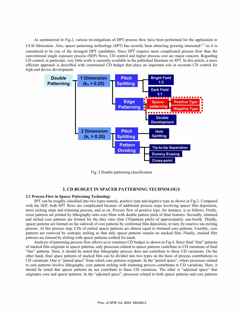
As summarized in Fig.2, various investigations of DPT process flow have been performed for the application to
ULSI fabrication. Also, spacer patterning technology (SPT) has recently been attracting growing interested[1]as it is considered to be one of the strongest DPT candidates. Since SPT requires more complicated process flow than the conventional single exposure process (SEP) flows, CD control and higher process cost are major concern. Regarding CD control, in particular, very little work is currently available in the published literature on SPT. In this article, a more efficient approach is described with constructed CD budget that plays an important role in accurate CD control for high-end device development.
Fig. 2 Double patterning classification
2. CD BUDGET IN SPACER PATTERNING TECHNOLOGY 2.1 Process Flow in Spacer Patterning Technology
SPT can be roughly classified into two types namely, positive type and negative type as shown in Fig.3. Compared with the SEP, both SPT flows are complicated because of additional process steps involving spacer film deposition, more etching steps and trimming process, and so on. Process flow of positive type, for instance, is as follows. Firstly, resist patterns are printed by lithography onto core films with double pattern pitch of final features. Secondly, trimmed and etched core patterns are formed for the duty ratio (line CD/pattern pitch) of approximately one-fourth. Thirdly, spacer patterns are formed on the sidewall of core patterns by conformal film deposition, in turn, by reactive ion etching process. At this process step, CDs of etched spacer patterns are almost equal to trimmed core patterns. Fourthly, core patterns are removed by isotropic etching so that only spacer patterns remain on stacked film. Finally, stacked film patterns are formed by etching with spacer patterns worked for mask.
Analysis of patterning process flow allows us to construct CD budget as shown in Fig.4. Since final “line” patterns of stacked film originate in spacer patterns, only processes related to spacer patterns contribute to CD variations of final “line” patterns. Here, it should be noted that lithography process does not contribute to these CD variations. On the other hand, final space patterns of stacked film can be divided into two types on the basis of process contributions to CD variations. One is “paired space” from which core patterns originate. In the “paired space”, where processes related to core patterns involve lithography, core pattern etching with trimming process contributes to CD variations. Here, it should be noted that spacer patterns do not contribute to these CD variations. The other is “adjoined space” that originates core and spacer patterns. In the “adjoined space”, processes related to both spacer patterns and core patterns
Double Patterning
1 Dimension (k1 < 0.25)
2 Dimension (k1 > 0.25)
Pitch Splitting
Edge Patterning
Pattern Dividing
Bright Field 1:3
Dark Field 3:1
Spacer patterning
Double Development
Pitch Splitting
Hole Splitting
Tip-to-tip Separation
Dummy Erasing
Cross-point
Positive Type
Negative Type
Double Patterning
1 Dimension (k1 < 0.25)
2 Dimension (k1 > 0.25)
Pitch Splitting
Edge Patterning
Pattern Dividing
Bright Field 1:3
Dark Field 3:1
Spacer patterning
Double Development
Pitch Splitting
Hole Splitting
Tip-to-tip Separation
Dummy Erasing
Cross-point
Positive Type
Negative Type
Proc. of SPIE Vol. 6924 692406-2

in SPT contribute to these CD variations.
Fig. 3 Process flow both single exposure process and spacer patterning process
Fig.4 Analysis of patterning process flow 2.2 CD Budget
Figure 5 summarizes error sources in both the SEP and the positive-type SPT. In the SEP, final “line” and “space” patterns of stacked film have the same error sources namely, lithography and stacked film etching. On the contrary in the SPT, error sources are provided in the three portions of grid patterns “line”, “paired space” and “adjoined space”. Studies of error sources in the positive-type SPT show that the amount of CD variations is in the following order “adjoined space” > “paired space” > “line”.
Single Exposure (SE)Negative type Positive type
Resist Line = Line Resist Line = Space
Litho.
Etch
SW Depo
Fill
remove
Etch
Hard mask
Core Film
Spacer patterning Process Flow (Two candidates)
Litho.
Etch
SW Depo
remove
Etch
Core Film
Hard mask
Single Exposure (SE)Negative type Positive type
Resist Line = Line Resist Line = Space
Litho.
Etch
SW Depo
Fill
remove
Etch
Hard mask
Core Film
Spacer patterning Process Flow (Two candidates)
Litho.
Etch
SW Depo
remove
Etch
Core Film
Hard mask
Litho.
Etch 1
SW Depo
remove
Etch 2
☆ Line→ Side wall Depo.
+ Etching
☆ Space (pair)→ Litho.+Etching(1)
+Etching(2)☆ Space (adjacent)→ Litho.+Etching(1)
+Side wall Depo.+Etching(2)
⊿ Sidewall× 2⊿ Sidewall× 2
Proc. of SPIE Vol. 6924 692406-3

Fig. 5 Error sources in both the SE and the positive-type SP Before constructing CD budget, we discuss how to construct and use CD budget in spacer patterning process. In
the conventional procedure, CD budget is constructed according to the requirements in total CD variations from devices. After that, this CD budget provided targets for CD variations for each unit process development. On the other hand, in spacer patterning, guidelines for CD variations for each unit process can produce CD budget. After that, this CD budget requires in total CD tolerance to device engineering.
Fig.6 How to construct and use CD Budget Based on the above concept, CD budgets for the SEP and the positive-type SPT are shown in Fig.7. Values of CD
variations in the budget are given as 3σ . Allowable CD variation for final patterns of the SEP was set at 14% of target
Litho.
SP (Positive type)
Line
Side Wall FilmDepo
Etch
Space(adjacent)
Origin Error source
Line Sidewall film Depo. / Etching
Space(Pair) Resist Line Litho. / Etching× 2
Space(adjacent) Resist Space Litho. / Etching× 2 / Depo.
SEOrigin Error source
Line Resist Line Litho. / Etching
Space Resist Space Litho. / Etching
Line Space
Litho.
Etch
Litho.
SP (Positive type)
Line
Side Wall FilmDepo
Etch
Space(adjacent)
Origin Error source
Line Sidewall film Depo. / Etching
Space(Pair) Resist Line Litho. / Etching× 2
Space(adjacent) Resist Space Litho. / Etching× 2 / Depo.
SEOrigin Error source
Line Resist Line Litho. / Etching
Space Resist Space Litho. / Etching
Line Space
Litho.
Etch
Conventional procedure New procedure in SPRequirements in total
CD variations from devices
Requirements in total CD variations from
devices
CD BudgetCD Budget
Targets in CD variations for each
unit process
Targets in CD variations for each
unit process Requirements in total
CD tolerance to devices
Requirements in total CD tolerance to
devices
Guidelines in CD variations for each unit
process
Guidelines in CD variations for each unit
process
CD BudgetCD Budget
Proc. of SPIE Vol. 6924 692406-4

CD for both “line” and “space”. In the CD budget for the SEP, 12% and 7.5% of target CD were set for lithography and etching, respectively.
In the positive-type SPT, on the other hand, allowable CD variations for final patterns were set at 10%, 17% and 20% of final target CD for “line”, “pared space” and “adjoined space”, respectively. In the CD budget of “line”, 7.5% and 6% of target CD were set for etching and spacer film deposition, respectively; those processes contribute to CD variations related to spacer patterns. In the CD budget of “paired space”, 12% and 10.6% of target CD were set for lithography and etching, respectively; those processes contribute to CD variations related to core patterns. In the CD budget of “adjoined space”, 12%, 10.6% and 12% of target CD were set for lithography, etching and spacer film deposition, respectively; those processes contribute to CD variations related to core patterns and spacer patterns. The etching error contributions of “paired space” and “adjoined space” are larger than that of “line” because there are more etching process steps for “paired space” and “adjoined space”. Also, the spacer film deposition error contribution of “adjoined space” is larger than that of “line” because there are CD variations on both sides for “adjoined space”.
Fig.7 CD budgets for the SEP and the positive-type SPT
3. EXPERIMANTAL VERIFICATIONS AND DISCUSSION 3.1 Process Trace and Process Window in the SPT
We applied the positive-type SPT to 35nm L/S pattern for process trace. The exposure was performed using ArF exposure system with 0.83NA and quadrupole illumination. CDs for each process step are shown in Fig.8. For three patterning portions of grid patterns, “line”, “paired space” and “adjoined space”, fabrication almost satisfied target feature sizes. In the process window, moreover, both lithography and final process step were verified in the focus window at 64nm L/S patterns and 32nm L/S patterns, respectively. The 1.0NA ArF immersion exposure tools with quadrupole illumination were used. Figure 9 demonstrates sufficient focus window, over 0.6um, for both lithography and final process step.
SpaceLine
TotalDepo.EtchLitho.
SpaceLine
TotalDepo.EtchLitho.
Space (Pair)Space (Adjacent)
LineTotalDepo.EtchLitho.
Space (Pair)Space (Adjacent)
LineTotalDepo.EtchLitho.
CD budget in Single Exposure (% to the final CD Target)
CD budget in Spacer Patterning (Posi.) (% to the final CD Target)
1212
7.57.5
1414
1212
7.510.610.6
6
12
101620
--
--
35nm HP SPT CD
20
30
40
50
60
70
80
Litho Etch+sliming SW Depo Remove Etch
CD[nm
]
Line
Spcce(Pair)
Space(Adj)
Proc. of SPIE Vol. 6924 692406-5

Fig.8 CDs for each process step (35nm L/S)
Fig. 9 Focus window verification
3.2 Verification of CD Budget Recently there has been growing recognition that LWR (line width roughness) is critical to line CD control. Figure
10 shows normalized LWR for 70nm L/S and 35nm L/S fabricated by SEP and SPT, respectively. This data indicates the LWR in 35nm L/S was smaller than the scaled value from 70nm L/S. This is probably because the LWR in SPT is smoothed by spacer formation process.
Fig. 10 Normalized LWR for 70nm L/S and 35nm L/S fabricated by SEP and SPT
Figure 11 shows normalized total CD variation for 70nm L/S and 32nm line, space(pair), and space(adj) fabricated by SEP and SPT, respectively. In spacer patterning process, CD variations in all three portions, line, pair spacer and adjacent space almost satisfied total CD variation in the budget. And we verified the order of the amount in each CD variation is ⊿ CDline < ⊿ CDspace(pair) <⊿ CDspace(Adjacent). Therefore, the total CD variation of the three portions was verified.
■ Litho.
■ Final
+0.1um -0.1um -0.2um -0.3umBest Focus+0.2um+0.3um
+0.1um -0.1um -0.2um -0.3umBest Focus+0.2um+0.3um
Range : 0.6um
Range : 0.6um
Litho. = 64nmnFinal = 32nmNA=1.0
Line width Roughness
0
0.2
0.4
0.6
0.8
1
1.2
70nm 35nmL/ S HP
LWR
(a.u
)
0
0.2
0.4
0.6
0.8
1
1.2Hp
Shr
ink
rate
vs
70nm
LWRHP shrink (vs 70nm)
Single exposure
Spacer patterning
Proc. of SPIE Vol. 6924 692406-6

Fig. 11 normalized total CD variation for 70nm L/S and
32nm line, space (pair), and space (adj) fabricated by SEP and SPT
3.3 Discussion In design for manufacturability (DfM) viewpoints, these process features should be taken into account in the device
engineering. Therefore for the successful implementation of spacer patterning technology in high-end devices, we propose a cross- functional development scheme encompassing device technologies and process technologies using the constructed CD budget. From the view point of lithography integration view points, we just integrate lithography unit processes to apply devices, so far. From now on, lithography integration should cover integration involving other unit processes for CD control using the CD budget.
Fig12 Lithography integration should cover integration involving
other unit processes for CD control using the CD budget.
Total CD Uniformity
0
0.2
0.4
0.6
0.8
1
1.2
70nm 32nmL/ S HP
CD U
nifo
rmity
(a.u
)
LineSpace(Pair)Space(Adj)
Lithography IntegrationLithography Integration
Litho. Integration
Mask
Resist
Metrology
OPC
Exp.Tool
Inspection
MaskMask
ResistResist
MetrologyMetrology
OPCOPC
Exp.ToolExp.Tool
InspectionInspection
Process Integration
Device & Design
Process Integration
Device & DesignD.R.D.R.DfMDfM
CMPCMPDryEtching
DryEtching
FilmFilmWet
EtchingWet
Etching
Proc. of SPIE Vol. 6924 692406-7

4. SUMMARY We constructed CD error budget for spacer patterning process (SP) to clarify each unit process contribution. Studies
of error sources in the positive-type SP show that the amount of CD variations is in the order “adjoined space” > “paired space” > “line”. We experimentally verified to the above CD budget. Each CD variation almost satisfied the budget. A successful SP implementation for devices requires an alternative approach encompassing device and process technology.
ACKNOWLEDGMENTS The authors are grateful to Dr.T.Higashiki and Mr.S.Inoue of Process & Manufacturing Engineering Center,
Semiconductor Company, Toshiba Corporation, for fruitful discussion and critical review of this paper.
REFERENCES [1] Woo-Yung Jung,et al., “Patterning with spacer for extending the resolution limit of current lithography tool” Proc. SPIE6156,2006
Proc. of SPIE Vol. 6924 692406-8