Embed Size (px)
Citation preview
Ana Paula Pinto Correia
Licenciada em Ciências da Engenharia de Micro e Nanotecnologias
A Second-Order ADC using sputtered IGZO TFTs with multilayer dielectric
Dissertação para obtenção do Grau de Mestre em Engenharia de Micro e Nanotecnologias
Júri:
Presidente: Prof. Doutor Rodrigo Ferrão de Paiva Martins Arguente: Prof. Doutor Nuno Filipe Silva Veríssimo Paulino Vogal: Prof. Doutor Pedro Miguel Cândido Barquinha
Novembro, 2014
Orientador: Doutor Pedro Miguel Cândido Barquinha, Professor Auxiliar, Faculdade de Ciências e Tecnologia, Universidade Nova de Lisboa
Co-orientador: Doutor João Carlos da Palma Goes, Professor Associado com Agregação, Faculdade de Ciências e Tecnologia, Universidade Nova de Lisboa

A Second-Order ΣΔ ADC using sputtered IGZO TFTs with multilayer dielectric
Copyright © Ana Paula Pinto Correia, Faculdade de Ciências e Tecnologia, Universidade Nova
de Lisboa
A Faculdade de Ciências e Tecnologia e a Universidade Nova de Lisboa têm o direito, perpétuo
e sem limites geográficos, de arquivar e publicar esta dissertação através de exemplares impressos
reproduzidos em papel ou de forma digital, ou por qualquer outro meio conhecido ou que venha a ser
inventado, e de a divulgar através de repositórios científicos e de admitir a sua cópia e distribuição
com objetivos educacionais ou de investigação, não comerciais, desde que seja dado crédito ao autor e
editor.

i
Acknowledgments
Coming together is a beginning; keeping together is progress; working together is success.
Henry Ford
There were hours, days, weeks, consecutive months of work, some frustration and much passion,
support and guidance. There were people, many people who, with a smile or just with simple
encouragement words, helped me to move forward and successfully complete an important stage of
my life.
Yes!, there were many people who, even in a simple way, contributed and collaborated on this
project – to all of them, my sincerely thank. However, it would be impossible not make reference of
some institutions and persons.
To my advisors, Prof. João Goes and Prof. Pedro Barquinha. Firstly, I must thank for the
excellent guidance and availability, making sure that without your support and trust, this
multidisciplinary project would not become possible. At the same time, your friendship has been, and
certainly will continue be!, a strong impulse to my personal and professional development.
To Materials Science Department, Electrical Engineering Department and, specially, to
CENIMAT/I3N, CEMOP and CTS/UNINOVA. All persons who form these institutions, allied to fully
equipped laboratories and formidable working conditions, provided a realization of a project with this
dimension. A particular and sincerely thank to Prof. Elvira Fortunato and Prof. Rodrigo Martins – your
effort has located this institution in a privileged place at the international level.
To Silicon & Software Systems (S3 Group) Portugal. Your support and friendship were essential
for my continue personal development and for an excellent professional integration. A special thank to
Ing. Arnaldo Guerreiro and Ing. Pedro Faria by all technical support.
To Materials for Electronics, Optoelectronics and Nanotechnologies Group. Your help with
different equipment, devices production and data obtaining were crucial. In addition, your friendship
improved my integration into the group. A sincerely thank to Ing. Ana Rovisco and Ing. Jorge Martins,
for their support in clean room, mainly in an initial period. To Dr. Asal Kiazadeh, Dr. Joana Pinto, Ing.
Sónia Pereira and Prof. Luís Pereira for helping me with characterization tools.
To all “nearly” Dr. from Micro and Nanolectronics Group (from CTS): Ing. Somayeh
Abdollahvand, Ing. Beatrice Moasa, Ing. Blazej Nowacki, Ing. Edinei Santin, Ing. Hugo Serra, Ing.
Ivan Bastos and Ing. João de Melo. Your readiness and willingness to help will always be remembered
here by the younger member of this room. I could not fail to make a reference to Ing. Edinei Santim
for helping me with transistor models and, a special mention to Ing. João de Melo by all support with
modulator and simulation tools.
To all my friends of Micro and Nanotechnologies Engineering and Materials Engineering. Your
friendship during this way was extremely important. A honestly thank to Daniel Matos, Gonçalo
Rodrigues, Inês Cunha, Miguel Soares, Paul Grey, Pedro Baião, and Vasco Rodrigues: I learned a lot
with you! A further reference to Catarina Rodrigues and Emanuel Carlos by the encouragement with
transistor models and comparator.
To all my friends from North. The distance is no impediment and this is the proof - even far
away, you are always close. Thanks for your support and friendship. A special thanks to Sara Pereira,
Tiago Cunha and Andreia Soares - your calls transmitting force and courage in the most difficult
moments will never be forgotten. Further reference to Luis Ribeiro - a future Electrical and Computer
Engineer!
To Ricardo Ferreira. Your patience, understanding, friendship and love over the years.
To my parents, brother and remaining family. It was with you, it was for you! You always will
be my pillar, my inspiration, my life. There is no way to express my gratitude, who I am today is due
to you, to your love. I love you!
To my beloved grandfather. My great and eternal support. Wherever you are, you will always be
in my heart.

ii
iii
Quem não sente a ânsia de ser mais, não chegará a ser nada.
Miguel de Unamuno

iv
v
Abstract
This dissertation combines materials science and electronics engineering to implement, for the
first time, a 2nd-order ∑∆ ADC using oxide TFTs. The transistors employ a sputtered IGZO
semiconductor and an optimized dielectric layer, based on mixtures of sputtered Ta2O5 and SiO2.
These dielectrics are studied in multilayer configurations, being the best results achieved for 7 layers:
IG<10 pA and EB>7.5 MV/cm, while keeping κ>10, yielding a major improvement over Ta2O5 single-
layer. After annealing at 200 °C, TFTs with these dielectrics exhibit µSAT≈13 cm2/Vs, On/Off≈107 and
S≈0.2 V/dec. An a-Si:H TFT RPI model is adapted to simulate these devices with good fitting to
experimental data. Concerning circuits, the ∑∆ architecture is naturally selected to deal with device
mismatch. After design optimization, ADC simulations achieve SNDR≈57 dB, DR≈65 dB and power
dissipation, approximately, of 22 mW (VDD=10 V), which are above the current state-of-the-art for
competing thin film technologies, such as organics or even LTPS. Mask layouts are currently under
verification to enable successful circuit fabrication in the next months.
This work is a major step towards the design of complex multifunctional electronic systems with
oxide TFT technology, being integrated in ongoing EU-funded and FCT-funded research projects at
CENIMAT and UNINOVA.
Keywords: a-IGZO TFTs; sputtered high-κ dielectrics; multicomponent and multilayers
dielectrics; ΣΔ Modulator; ADC.

vi
vii
Resumo
Esta dissertação combina Ciência dos Materiais e Engenharia Eletrotécnica para implementar,
pela primeira vez, um ∑∆ ADC de 2ª-ordem usando TFTs de óxido. Os transístores empregam IGZO
como semicondutor e um dielétrico baseado em misturas de Ta2O5 e SiO2, sendo todos os materiais
depositados por pulverização-catódica. Os dieléctricos são estudados em configurações multicamada,
sendo o melhor resultado obtido para 7 camadas: IG<10 pA e EB>7.5 MV/cm, mantendo κ>10. Depois
de recozidos a 200 °C, os TFTs exibem µSAT≈13 cm2/Vs, On/Off≈107 e S≈0.2 V/dec. O modelo a-Si:H
TFT RPI é adaptado para simular estes dispositivos com bom ajuste aos dados experimentais.
Relativamente aos circuitos, a arquitectura por modulação ∑∆ é selecionada para lidar com a variação
de desempenho e erros de emparelhamento entre transístores. Após optimização do circuito, as
simulações do ADC revelaram: SNDR≈57 dB, DR≈65 dB e dissipação de potência ≈22 mW (VDD=10
V), valores melhores que os permitidos por outras tecnologias de filme fino, como orgânicos ou
mesmo LTPS. Actualmente, o desenho das máscaras está sob verificações finais para permitir o
fabrico do circuito nos próximos meses.
Este trabalho contribui fortemente para projetar sistemas eletrónicos multifuncionais e
complexos com TFTs de óxidos, sendo integrado em projetos de investigação em curso financiados
pela UE e FCT no CENIMAT e no CTS/ UNINOVA.
Palavras-chave: a-IGZO TFTs; Dielétricos de elevada permitividade depositados por
pulverização-catódica; Dielétricos multicompostos e multicamadas; Modulador ΣΔ; ADC.

viii
ix
Contents
1. Motivation, thesis contribution and structure ................................................................ 1
1.1 Contributions ................................................................................................................... 2
1.2 Thesis Structure ............................................................................................................... 2
2. Introduction ....................................................................................................................... 3
2.1 Thin-Film Transistors ...................................................................................................... 3
2.1.1 TFTs structure and operation ................................................................................... 3
2.1.2 From conceptual patents to oxide TFTs .................................................................. 3
2.2 Analog-to-digital converters ............................................................................................ 6
2.2.1 ΣΔ Modulators ......................................................................................................... 7
2.2.2 ADCs using TFTs .................................................................................................... 8
3. Materials and techniques .................................................................................................. 9
3.1 Production techniques ..................................................................................................... 9
3.1.1 Sputtering ................................................................................................................ 9
3.1.2 Patterning ............................................................................................................... 10
3.2 Characterization techniques........................................................................................... 10
3.3 Modeling, Simulation and EDA tools ........................................................................... 10
4. Results and Discussion .................................................................................................... 11
4.1 Amorphous multicomponent high-κ dielectrics based on Ta2O5 and SiO2: thin films and
integration in IGZO TFTs ................................................................................................................. 11
4.1.1 Single layer structure using Ta2O5 and TSiO ........................................................ 11
4.1.2 Multilayer structures based on TSiO and SiO2 ...................................................... 18
4.1.3 IGZO TFT Modeling ............................................................................................. 22
4.2 ΣΔ Modulator: circuit and simulation results ................................................................ 23
4.2.1 Comparator ............................................................................................................ 23
4.2.2 ΣΔ Modulator ........................................................................................................ 26
4.3 Circuit Layout ................................................................................................................ 29
5. Conclusions and Future Perspectives ............................................................................ 31
x
5.1 Conclusions ................................................................................................................... 31
5.2 Future Perspectives ........................................................................................................ 32
6. References ........................................................................................................................ 33
Appendix A - ADCs using TFTs ............................................................................................... 37
Appendix B - TFT production by steps ..................................................................................... 39
Appendix C - Deposition conditions for Mo and IGZO ........................................................... 41
Appendix D - Characterization techniques ............................................................................... 43
Appendix E - Electrical Characterization of devices using Ta2O5 and TSiO ............................ 45
Appendix F - RBS results ......................................................................................................... 49
Appendix G - Electrical Characterization of devices using Multilayer structures .................... 51
Appendix H - ΣΔ Modulator ..................................................................................................... 55
Appendix I - Circuit Layout ...................................................................................................... 57
xi
List of Figures
Figure 1.1 - Concepts of transparent displays: smart window (a) [1]. Concepts of flexible
displays: watch (b) [2] and a display developed by HP Lab (c) [3]. ..................................................... 1
Figure 2.1 – Ideal output characteristics of a n-type TFT (adapted from [5]). ............................. 3
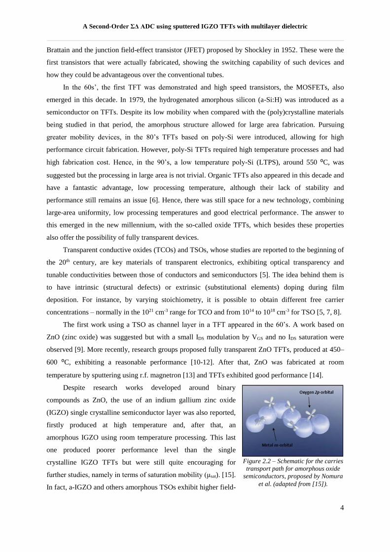
Figure 2.2 – Schematic for the carries transport path for amorphous oxide semiconductors,
proposed by Nomura et al. (adapted from [15]). .................................................................................... 4
Figure 2.3 – Inversely proportional relation between band gap and κ for some dielectrics
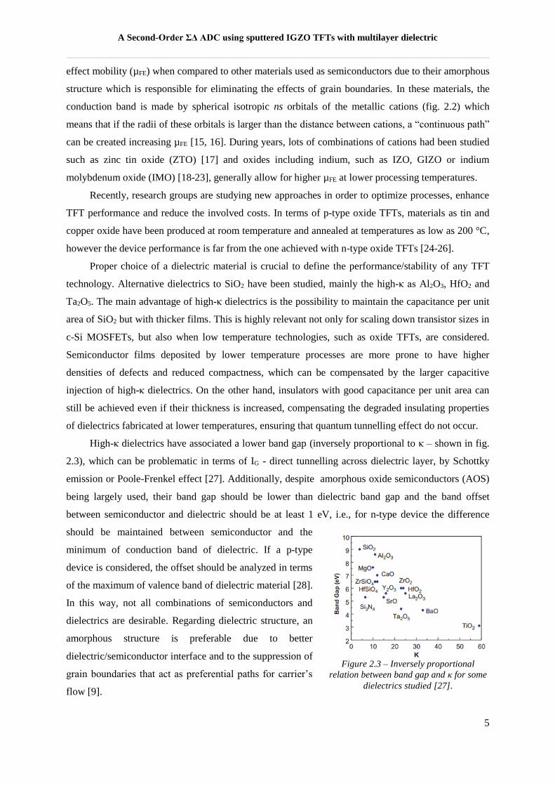
studied [27]. ............................................................................................................................................ 5
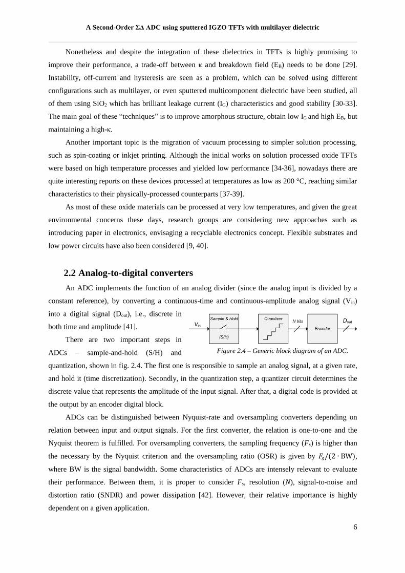
Figure 2.4 – Generic block diagram of an ADC. ........................................................................... 6
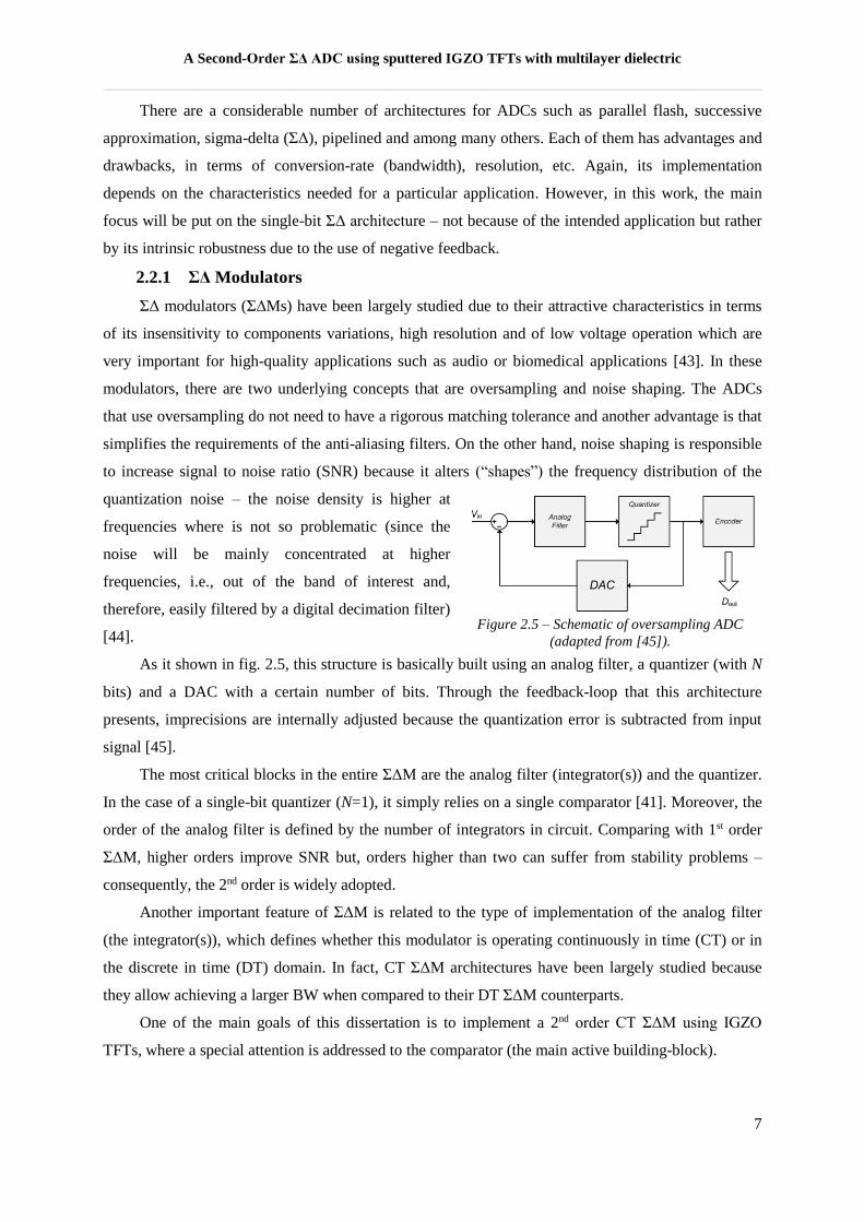
Figure 2.5 – Schematic of oversampling ADC (adapted from [45]). ............................................. 7
Figure 3.1 – TFT structure: staggered bottom gate, top-contacts. ................................................ 9
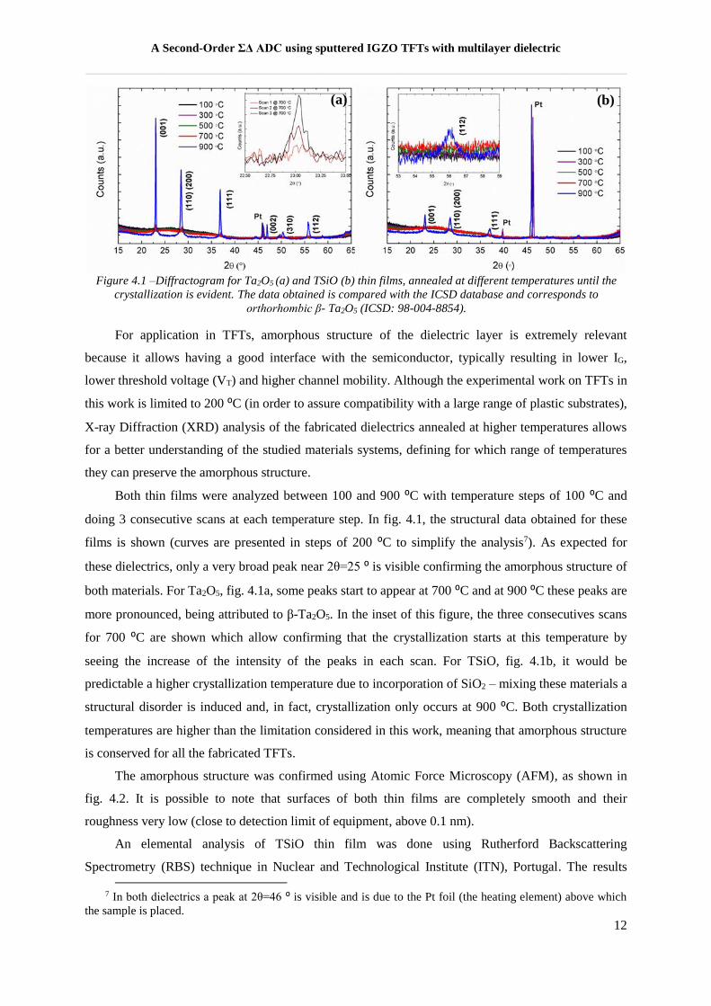
Figure 4.1 –Diffractogram for Ta2O5 (a) and TSiO (b) thin films, annealed at different
temperatures until the crystallization is evident. The data obtained is compared with the ICSD
database and corresponds to orthorhombic β- Ta2O5 (ICSD: 98-004-8854). ...................................... 12
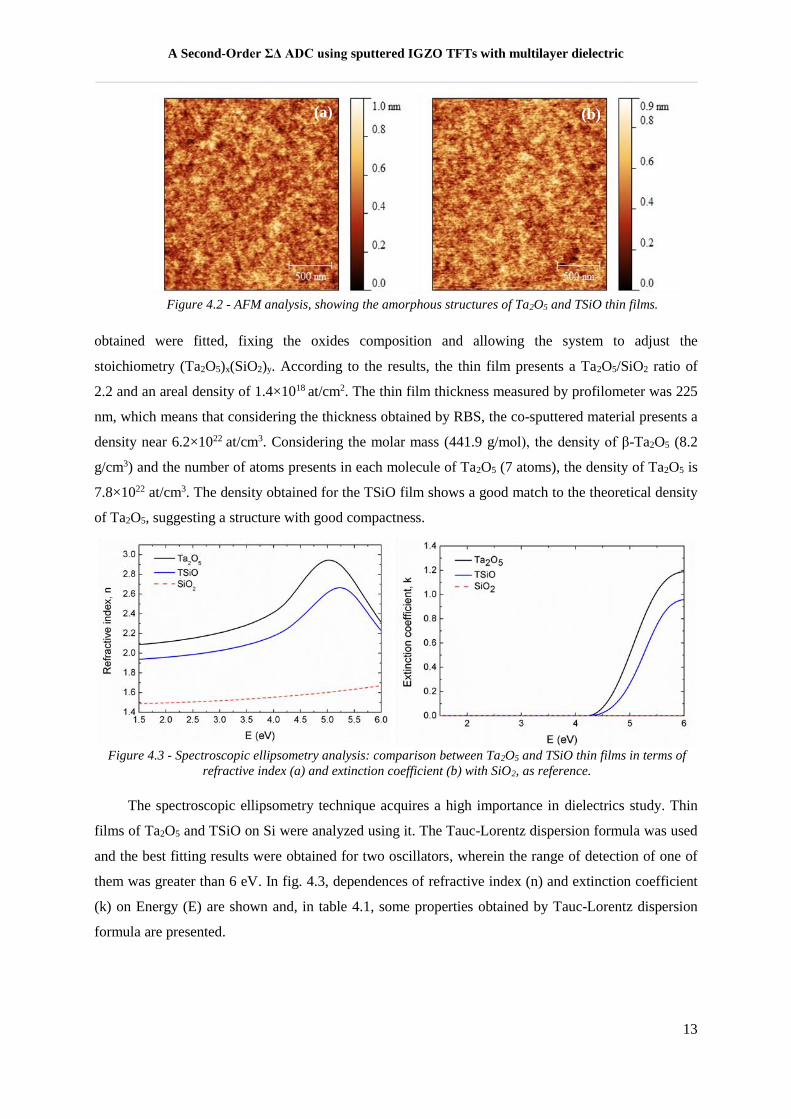
Figure 4.2 - AFM analysis, showing the amorphous structures of Ta2O5 and TSiO thin films. .. 13
Figure 4.3 - Spectroscopic ellipsometry analysis: comparison between Ta2O5 and TSiO thin
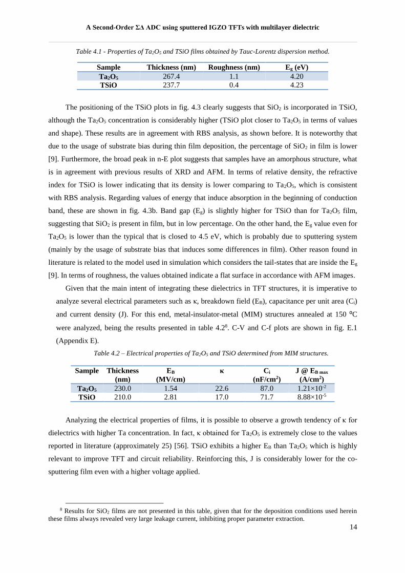
films in terms of refractive index (a) and extinction coefficient (b) with SiO2, as reference. ................ 13
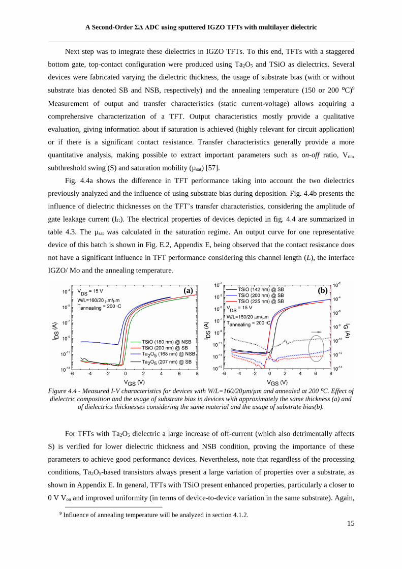
Figure 4.4 - Measured I-V characteristics for devices with W/L=160/20µm/µm and annealed at
200 ⁰C. Effect of dielectric composition and the usage of substrate bias in devices with approximately
the same thickness (a) and of dielectrics thicknesses considering the same material and the usage of
substrate bias(b). ................................................................................................................................... 15
Figure 4.5 – Von and S variations during stress and recovery measurements for TFTs annealed at
200 ⁰C using Ta2O5 and TSiO as dielectric layer for TFTs with W/L = 160/20 µm/µm, applying a gate
field of 0.16MV.cm-1 in dark (a). Solid and open circles denote ΔVon and ΔS, respectively. Mechanisms
involved in AOS and dielectric materials, when a positive gate bias stress is applied in a staggered
bottom gate, top contacts structure (b) (adapted from [58]). ............................................................... 17
Figure 4.6 – Compositional analysis: comparison between TSiO and multilayers using three and
five layers. ............................................................................................................................................. 18
Figure 4.7 - Spectroscopic ellipsometry analysis: comparison between single and multilayers
dielectrics thin films in terms of refractive index (a) and extinction coefficient (b) with SiO2, as
reference. ............................................................................................................................................... 19
Figure 4.8 - Measured I-V characteristics for devices annealed at different temperature and
evaluated in different times, using a medium integration time (a). Effect of integration time in I-V
characteristics (b). ................................................................................................................................ 20
Figure 4.9 - Measured I-V characteristics for multilayer structures wherein it is shown the IG. 21
xii
Figure 4.10 - Von and S variations during stress and recovery measurements for TFTs annealed
at 200 ⁰C using multilayers structures (W/L = 160/20 µm/µm), applying a gate field of 0.16MV.cm-1.
Solid and open circles denote ΔVon and ΔS, respectively. ..................................................................... 21
Figure 4.11 - Measured and simulated I-V characteristics for a multilayer device (3 layers) with
W/L=160/20 µm/µm: transfer curve (a) and output curve (b). ............................................................. 22
Figure 4.12 – Schematic of the proposed comparator: pre-amplifier (pre-amp) (a); positive-
feedback latch (PFBL) (b); logic inverter (c) and complete comparator (d). ....................................... 24
Figure 4.13 – Differential output when a input triangular signal is applied (a). Differential
signal with a sequence of eight different comparisons (b). ................................................................... 24
Figure 4.14 - Simulated 1-σ random offset voltage (σ(VON) = 50 mV) for VON=0 V @ IB=50 µA
(a) and VON=0.5 V @ IB=30 µA (b). ...................................................................................................... 25
Figure 4.15 - Schematic differential 2nd order CT ΣΔM with feedforward structure: transmission
gate D-type fli- flop (a) and the modulator (b)...................................................................................... 27
Figure 4.16 – Simulated FFT assuming a -6dBFS and 100 Hz input signal. ............................... 28
Figure 4.17 – Obtained output spectrum obtained from electrical simulation of the complete ΣΔ
Modulator (SNDR versus input signal amplitude and SNR versus input signal amplitude). ................ 28
Figure 4.18 - Layout of the ΣΔM. ................................................................................................ 30
Figure B.1 - Sequence of steps during a sputtered TFT production. The microscope image was
obtained using Olympus BX51 (100x). .................................................................................................. 39
Figure E.1 - C-f and C-V characteristics of MIM structures that integrated Ta2O5 and TSiO
layers. .................................................................................................................................................... 45
Figure E.2 - Output characteristics of IGZO TFTs with Mo electrodes, using TSiO as dielectric
layer (≈200 nm), annealed at 200 ⁰C. ................................................................................................... 45
Figure E.3 - SEM image of Mo/ dielectric interface, where the “bubbles” effect is visible. ...... 46
Figure E.4 - Transfer curves for different devices (from right to left) in the same substrate, using
Ta2O5 (a) and TSiO (b) with a thickness close to 200 nm and annealed at 200 ⁰C. Both dielectrics
were deposited by sputtering with substrate bias. ................................................................................. 47
Figure E.5 - Transfer curves in double sweep mode using Ta2O5 (a) and TSiO (b) with a
thickness close to 200 nm and annealed at 200 ⁰C. Both dielectrics were deposited by sputtering with
substrate bias ......................................................................................................................................... 47
Figure E.6 - Transfer characteristics evolution for stress and recovery for Ta2O5, (a) and (b),
and for TSiO (c) and (d). ....................................................................................................................... 48
Figure F.1 - Composition analysis obtained by RBS for IGZO film. .......................................... 49
Figure G.1 - Transfer characteristics evolution for stress and recovery for multilayer (3 layers),
(a) and (b), and for multilayer (7 layers) (c) and (d). ........................................................................... 52
Figure G.2 - Cross section of TFT near the channel (SEM image). ........................................... 53
xiii
Figure H.1 - Simulation result for inverter considering the load n-type TFT (40/10 µm/µm) and
driver (160/10 µm/µm). ......................................................................................................................... 55
Figure I.1 - Structure of PCELL used for a 160/10 (µm/µm). .................................................... 57
Figure I.2 - Glass substrate, covered with a Mo thin film, inserted in a PCI connector for
testing. ................................................................................................................................................... 57

xiv
xv
List of Tables
Table 3.1 - Deposition conditions for dielectric layer. All sputtering targets were performed by
SCM.inc. .................................................................................................................................................. 9
Table 4.1 - Properties of Ta2O5 and TSiO films obtained by Tauc-Lorentz dispersion method. . 14
Table 4.2 – Electrical properties of Ta2O5 and TSiO determined from MIM structures. ............ 14
Table 4.3 – Summary of electrical properties of devices annealed at 200 ⁰C using different
dielectrics in different conditions, depicted in fig. 4.4. ......................................................................... 16
Table 4.4 - Properties of single and multilayers films obtained by Tauc-Lorentz dispersion
method. .................................................................................................................................................. 19
Table 4.5 - Electrical properties of dielectrics determined from MIM structures. ...................... 20
Table 4.6 – Simulated key performance parameters. ................................................................... 25
Table 4.7 – Simulated comparator’s offset with different Von. ..................................................... 26
Table 4.8 – Main characteristics of ΣΔM. ................................................................................... 28
Table A.1 - ADCs using Thin Film Technologies. ....................................................................... 37
Table C.1 - Deposition conditions for contacts (Mo) and semiconductor layers (IGZO) by
sputtering. All sputtering targets were performed by SCM.inc. ............................................................ 41
Table D.1 - Main goals and experimental details of characterization techniques used during this
work. ...................................................................................................................................................... 43
Table F.1 - Parameters obtained for dielectrics after fitting for RBS results. ............................ 49
Table F.2 - RBS results obtained after fitting of IGZO data. ...................................................... 50
Table G.1 - Electrical properties for TFT devices that used multilayers structures (W/L =
160/20 µm/µm). Devices were measured using a short integration time to prevent hump effects (see
chapter 4), which increases the measured IG values over more conventional medium integration times.
............................................................................................................................................................... 51
Table H.1 - Transistor dimensions used in the initial sizing of the comparator. ........................ 55
Table H.2 - Transistor dimensions used in the final sizing of the comparator. .......................... 56
Table H.3 - Sizing of passive elements obtained by SIMULINK®. ............................................. 56
Table I.1 - Rules used during circuit layout. ............................................................................... 57

xvi
xvii
Symbols
Ci –Gate capacitance per unit area
EB – Breakdown field
EC – Conduction band
Eg – Bandgap
Fs – Sampling frequency
IDS – Drain-to-source current
IG – Gate leakage current
J – Current density
k – Extinction coefficient
L – Channel length
n – Refractive index
S – Subthreshold slope
VDD – Power supply
VDS – Drain voltage
VGS – Gate voltage
Von - Turn-on voltage
VT – Threshold voltage
W – Channel width
κ – Dielectric constant
µFE – Field-effect mobility
µsat – Saturation mobility
χ2 – Error function

xviii
xix
Acronyms
ADC – Analog-to-digital converter
AFM – Atomic force microscopy
AOS – Amorphous oxide semiconductors
BW – Bandwidth
CENIMAT – Centro de Investigação de Materiais
CEMOP - Center of Excellence in Microelectronics Optoelectronics and Processes
CT – Continuous time
CTS - Centre of Technology and Systems
CMOS – Complementary metal oxide semiconductor
DAC – Digital-to-analog converter
DNL – Differential non-linearity
DR – Dynamic range
DRC – Design rule check
DSP – Digital signal processor
DT – Discrete time
EDA – Electronic design automation
ENOB – Effective number of bits
FFT – Fast Fourier Transform
IC – Integrated circuit
IGZO – Gallium indium zinc oxide
INL – Integral non-linearity
LSB – Least significant bit
LTPS – Low temperature polycrystalline silicon
LVS – Layout versus schematic
MESFET – Metal semiconductor field effect transistor
MIM – Metal-insulator-metal
MIS – Metal-insulator-semiconductor
MISFET - Metal insulator field effect transistor
MOSFET – Metal oxide semiconductor field effect transistor
OSR – Oversampling ratio
PDK – Process-design-kit
PFBL – Positive feedback latch
RBS – Rutherford backscattering spectroscopy
SEM – Scanning electron microscopy
xx
SNDR – Signal-to-noise plus distortion ratio
SNR – Signal to noise ratio
TCO – Transparent conducting oxide
TFT – Thin-film transistor
TSO – Transparent semiconducting oxide
UNINOVA – Instituto de Desenvolvimento de Novas Tecnologias
XRD – X-ray diffraction
∑∆ - Sigma-delta
∑∆M - Sigma-delta modulator
A Second-Order ΣΔ ADC using sputtered IGZO TFTs with multilayer dielectric
__________________________________________________________________________________
1
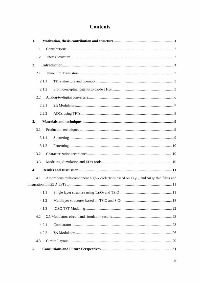
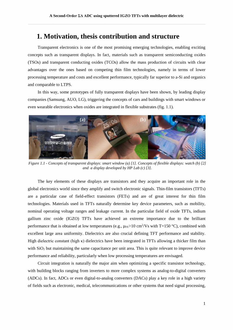
Figure 1.1 - Concepts of transparent displays: smart window (a) [1]. Concepts of flexible displays: watch (b) [2]
and a display developed by HP Lab (c) [3].
(a) (b) (c)
1. Motivation, thesis contribution and structure
Transparent electronics is one of the most promising emerging technologies, enabling exciting
concepts such as transparent displays. In fact, materials such as transparent semiconducting oxides
(TSOs) and transparent conducting oxides (TCOs) allow the mass production of circuits with clear
advantages over the ones based on competing thin film technologies, namely in terms of lower
processing temperature and costs and excellent performance, typically far superior to a-Si and organics
and comparable to LTPS.
In this way, some prototypes of fully transparent displays have been shown, by leading display
companies (Samsung, AUO, LG), triggering the concepts of cars and buildings with smart windows or
even wearable electronics when oxides are integrated in flexible substrates (fig. 1.1).
The key elements of these displays are transistors and they acquire an important role in the
global electronics world since they amplify and switch electronic signals. Thin-film transistors (TFTs)
are a particular case of field-effect transistors (FETs) and are of great interest for thin film
technologies. Materials used in TFTs naturally determine key device parameters, such as mobility,
nominal operating voltage ranges and leakage current. In the particular field of oxide TFTs, indium
gallium zinc oxide (IGZO) TFTs have achieved an extreme importance due to the brilliant
performance that is obtained at low temperatures (e.g., µFE>10 cm2/Vs with T=150 °C), combined with
excellent large area uniformity. Dielectrics are also crucial defining TFT performance and stability.
High dielectric constant (high κ) dielectrics have been integrated in TFTs allowing a thicker film than
with SiO2 but maintaining the same capacitance per unit area. This is quite relevant to improve device
performance and reliability, particularly when low processing temperatures are envisaged.
Circuit integration is naturally the major aim when optimizing a specific transistor technology,
with building blocks ranging from inverters to more complex systems as analog-to-digital converters
(ADCs). In fact, ADCs or even digital-to-analog converters (DACs) play a key role in a high variety
of fields such as electronic, medical, telecommunications or other systems that need signal processing,
A Second-Order ΣΔ ADC using sputtered IGZO TFTs with multilayer dielectric
__________________________________________________________________________________
2
because despite all real signals are analog it is always desirable to process them, as much as possible,
in the digital domain.
Successful design, simulation and fabrication of an ADC is thus a very significant demonstration
of the capability of a TFT technology.
1.1 Contributions
Based on this background, the main contributions of this work are:
Optimization of sputtered dielectrics for increased breakdown field and improved IGZO TFT
reliability/performance. This includes the study of single layers (SiO2, Ta2O5 and TSiO) and their
integration in multilayer structures;
Adjust a model based on a-Si:H TFT model developed by Semiconductor Devices Research
Group at RPI, in order to simulate the optimized IGZO TFT behavior;
Design (circuit schematic and mask layout) of a robust second-order sigma-delta (ΣΔ) ADC
based in a power-optimized ΣΔ modulator (ΣΔM), where a special relevance is given to the most
critical analog active block – the comparator1.
Produce the circuit prototype and experimentally evaluate it - a future contribution.
1.2 Thesis Structure
The structure of this thesis is as follows:
In Chapter 2 is presented some background related to oxide semiconductors and high-κ
dielectrics used in TFTs. The operation mode of TFTs and a brief state of the art in this area are also
reported. Another section comprises operation of ADCs, some architectures and a concise state of the
art about ADCs using TFTs;
Chapter 3 summarizes the production technique (sputtering) and materials used during this
thesis work. Characterization techniques and EDA tools are also referred;
Chapter 4 comprises presentation and discussion of the obtained results during the study of
dielectric films and their application to IGZO TFTs. Besides experimental data, device simulation
results are also included. The adapted TFT model is then used to simulate the complete designed
ΣΔM. Finally, some circuit layout considerations are provided;
The main conclusions and some future perspectives based on the outputs of this work are
included in Chapter 5.
1 As a standard procedure, it has been assumed that the decimation filter will be implemented in the digital-
signal processor (DSP) usually available at system level.
A Second-Order ΣΔ ADC using sputtered IGZO TFTs with multilayer dielectric
__________________________________________________________________________________
3
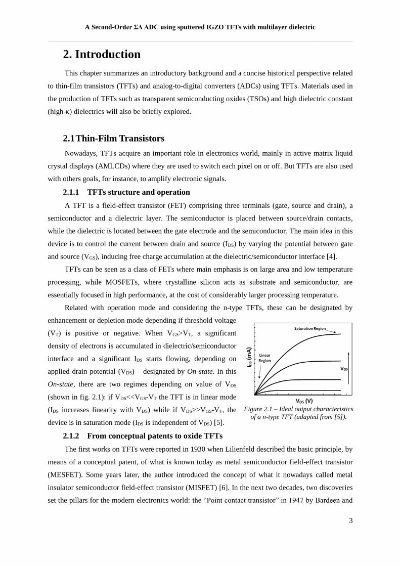
Figure 2.1 – Ideal output characteristics
of a n-type TFT (adapted from [5]).
2. Introduction
This chapter summarizes an introductory background and a concise historical perspective related
to thin-film transistors (TFTs) and analog-to-digital converters (ADCs) using TFTs. Materials used in
the production of TFTs such as transparent semiconducting oxides (TSOs) and high dielectric constant
(high-κ) dielectrics will also be briefly explored.
2.1 Thin-Film Transistors
Nowadays, TFTs acquire an important role in electronics world, mainly in active matrix liquid
crystal displays (AMLCDs) where they are used to switch each pixel on or off. But TFTs are also used
with others goals, for instance, to amplify electronic signals.
2.1.1 TFTs structure and operation
A TFT is a field-effect transistor (FET) comprising three terminals (gate, source and drain), a
semiconductor and a dielectric layer. The semiconductor is placed between source/drain contacts,
while the dielectric is located between the gate electrode and the semiconductor. The main idea in this
device is to control the current between drain and source (IDS) by varying the potential between gate
and source (VGS), inducing free charge accumulation at the dielectric/semiconductor interface [4].
TFTs can be seen as a class of FETs where main emphasis is on large area and low temperature
processing, while MOSFETs, where crystalline silicon acts as substrate and semiconductor, are
essentially focused in high performance, at the cost of considerably larger processing temperature.
Related with operation mode and considering the n-type TFTs, these can be designated by
enhancement or depletion mode depending if threshold voltage
(VT) is positive or negative. When VGS>VT, a significant
density of electrons is accumulated in dielectric/semiconductor
interface and a significant IDS starts flowing, depending on
applied drain potential (VDS) – designated by On-state. In this
On-state, there are two regimes depending on value of VDS
(shown in fig. 2.1): if VDS<<VGS-VT the TFT is in linear mode
(IDS increases linearity with VDS) while if VDS>>VGS-VT, the
device is in saturation mode (IDS is independent of VDS) [5].
2.1.2 From conceptual patents to oxide TFTs
The first works on TFTs were reported in 1930 when Lilienfeld described the basic principle, by
means of a conceptual patent, of what is known today as metal semiconductor field-effect transistor
(MESFET). Some years later, the author introduced the concept of what it nowadays called metal
insulator semiconductor field-effect transistor (MISFET) [6]. In the next two decades, two discoveries
set the pillars for the modern electronics world: the “Point contact transistor” in 1947 by Bardeen and
A Second-Order ΣΔ ADC using sputtered IGZO TFTs with multilayer dielectric
__________________________________________________________________________________
4
Figure 2.2 – Schematic for the carries
transport path for amorphous oxide
semiconductors, proposed by Nomura
et al. (adapted from [15]).
Brattain and the junction field-effect transistor (JFET) proposed by Shockley in 1952. These were the
first transistors that were actually fabricated, showing the switching capability of such devices and
how they could be advantageous over the conventional tubes.
In the 60s’, the first TFT was demonstrated and high speed transistors, the MOSFETs, also
emerged in this decade. In 1979, the hydrogenated amorphous silicon (a-Si:H) was introduced as a
semiconductor on TFTs. Despite its low mobility when compared with the (poly)crystalline materials
being studied in that period, the amorphous structure allowed for large area fabrication. Pursuing
greater mobility devices, in the 80’s TFTs based on poly-Si were introduced, allowing for high
performance circuit fabrication. However, poly-Si TFTs required high temperature processes and had
high fabrication cost. Hence, in the 90’s, a low temperature poly-Si (LTPS), around 550 ⁰C, was
suggested but the processing in large area is not trivial. Organic TFTs also appeared in this decade and
have a fantastic advantage, low processing temperature, although their lack of stability and
performance still remains an issue [6]. Hence, there was still space for a new technology, combining
large-area uniformity, low processing temperatures and good electrical performance. The answer to
this emerged in the new millennium, with the so-called oxide TFTs, which besides these properties
also offer the possibility of fully transparent devices.
Transparent conductive oxides (TCOs) and TSOs, whose studies are reported to the beginning of
the 20th century, are key materials of transparent electronics, exhibiting optical transparency and
tunable conductivities between those of conductors and semiconductors [5]. The idea behind them is
to have intrinsic (structural defects) or extrinsic (substitutional elements) doping during film
deposition. For instance, by varying stoichiometry, it is possible to obtain different free carrier
concentrations – normally in the 1021 cm-3 range for TCO and from 1014 to 1018 cm-3 for TSO [5, 7, 8].
The first work using a TSO as channel layer in a TFT appeared in the 60’s. A work based on
ZnO (zinc oxide) was suggested but with a small IDS modulation by VGS and no IDS saturation were
observed [9]. More recently, research groups proposed fully transparent ZnO TFTs, produced at 450–
600 ⁰C, exhibiting a reasonable performance [10-12]. After that, ZnO was fabricated at room
temperature by sputtering using r.f. magnetron [13] and TFTs exhibited good performance [14].
Despite research works developed around binary
compounds as ZnO, the use of an indium gallium zinc oxide
(IGZO) single crystalline semiconductor layer was also reported,
firstly produced at high temperature and, after that, an
amorphous IGZO using room temperature processing. This last
one produced poorer performance level than the single
crystalline IGZO TFTs but were still quite encouraging for
further studies, namely in terms of saturation mobility (μsat). [15].
In fact, a-IGZO and others amorphous TSOs exhibit higher field-
A Second-Order ΣΔ ADC using sputtered IGZO TFTs with multilayer dielectric
__________________________________________________________________________________
5
Figure 2.3 – Inversely proportional
relation between band gap and κ for some
dielectrics studied [27].
effect mobility (µFE) when compared to other materials used as semiconductors due to their amorphous
structure which is responsible for eliminating the effects of grain boundaries. In these materials, the
conduction band is made by spherical isotropic ns orbitals of the metallic cations (fig. 2.2) which
means that if the radii of these orbitals is larger than the distance between cations, a “continuous path”
can be created increasing µFE [15, 16]. During years, lots of combinations of cations had been studied
such as zinc tin oxide (ZTO) [17] and oxides including indium, such as IZO, GIZO or indium
molybdenum oxide (IMO) [18-23], generally allow for higher µFE at lower processing temperatures.
Recently, research groups are studying new approaches in order to optimize processes, enhance
TFT performance and reduce the involved costs. In terms of p-type oxide TFTs, materials as tin and
copper oxide have been produced at room temperature and annealed at temperatures as low as 200 °C,
however the device performance is far from the one achieved with n-type oxide TFTs [24-26].
Proper choice of a dielectric material is crucial to define the performance/stability of any TFT
technology. Alternative dielectrics to SiO2 have been studied, mainly the high-κ as Al2O3, HfO2 and
Ta2O5. The main advantage of high-κ dielectrics is the possibility to maintain the capacitance per unit
area of SiO2 but with thicker films. This is highly relevant not only for scaling down transistor sizes in
c-Si MOSFETs, but also when low temperature technologies, such as oxide TFTs, are considered.
Semiconductor films deposited by lower temperature processes are more prone to have higher
densities of defects and reduced compactness, which can be compensated by the larger capacitive
injection of high-κ dielectrics. On the other hand, insulators with good capacitance per unit area can
still be achieved even if their thickness is increased, compensating the degraded insulating properties
of dielectrics fabricated at lower temperatures, ensuring that quantum tunnelling effect do not occur.
High-κ dielectrics have associated a lower band gap (inversely proportional to κ – shown in fig.
2.3), which can be problematic in terms of IG - direct tunnelling across dielectric layer, by Schottky
emission or Poole-Frenkel effect [27]. Additionally, despite amorphous oxide semiconductors (AOS)
being largely used, their band gap should be lower than dielectric band gap and the band offset
between semiconductor and dielectric should be at least 1 eV, i.e., for n-type device the difference
should be maintained between semiconductor and the
minimum of conduction band of dielectric. If a p-type
device is considered, the offset should be analyzed in terms
of the maximum of valence band of dielectric material [28].
In this way, not all combinations of semiconductors and
dielectrics are desirable. Regarding dielectric structure, an
amorphous structure is preferable due to better
dielectric/semiconductor interface and to the suppression of
grain boundaries that act as preferential paths for carrier’s
flow [9].
A Second-Order ΣΔ ADC using sputtered IGZO TFTs with multilayer dielectric
__________________________________________________________________________________
6
Figure 2.4 – Generic block diagram of an ADC.
Nonetheless and despite the integration of these dielectrics in TFTs is highly promising to
improve their performance, a trade-off between κ and breakdown field (EB) needs to be done [29].
Instability, off-current and hysteresis are seen as a problem, which can be solved using different
configurations such as multilayer, or even sputtered multicomponent dielectric have been studied, all
of them using SiO2 which has brilliant leakage current (IG) characteristics and good stability [30-33].
The main goal of these “techniques” is to improve amorphous structure, obtain low IG and high EB, but
maintaining a high-κ.
Another important topic is the migration of vacuum processing to simpler solution processing,
such as spin-coating or inkjet printing. Although the initial works on solution processed oxide TFTs
were based on high temperature processes and yielded low performance [34-36], nowadays there are
quite interesting reports on these devices processed at temperatures as low as 200 °C, reaching similar
characteristics to their physically-processed counterparts [37-39].
As most of these oxide materials can be processed at very low temperatures, and given the great
environmental concerns these days, research groups are considering new approaches such as
introducing paper in electronics, envisaging a recyclable electronics concept. Flexible substrates and
low power circuits have also been considered [9, 40].
2.2 Analog-to-digital converters
An ADC implements the function of an analog divider (since the analog input is divided by a
constant reference), by converting a continuous-time and continuous-amplitude analog signal (Vin)
into a digital signal (Dout), i.e., discrete in
both time and amplitude [41].
There are two important steps in
ADCs – sample-and-hold (S/H) and
quantization, shown in fig. 2.4. The first one is responsible to sample an analog signal, at a given rate,
and hold it (time discretization). Secondly, in the quantization step, a quantizer circuit determines the
discrete value that represents the amplitude of the input signal. After that, a digital code is provided at
the output by an encoder digital block.
ADCs can be distinguished between Nyquist-rate and oversampling converters depending on
relation between input and output signals. For the first converter, the relation is one-to-one and the
Nyquist theorem is fulfilled. For oversampling converters, the sampling frequency (Fs) is higher than
the necessary by the Nyquist criterion and the oversampling ratio (OSR) is given by 𝐹𝑠/(2 ∙ BW),
where BW is the signal bandwidth. Some characteristics of ADCs are intensely relevant to evaluate
their performance. Between them, it is proper to consider Fs, resolution (N), signal-to-noise and
distortion ratio (SNDR) and power dissipation [42]. However, their relative importance is highly
dependent on a given application.
A Second-Order ΣΔ ADC using sputtered IGZO TFTs with multilayer dielectric
__________________________________________________________________________________
7
There are a considerable number of architectures for ADCs such as parallel flash, successive
approximation, sigma-delta (ΣΔ), pipelined and among many others. Each of them has advantages and
drawbacks, in terms of conversion-rate (bandwidth), resolution, etc. Again, its implementation
depends on the characteristics needed for a particular application. However, in this work, the main
focus will be put on the single-bit ΣΔ architecture – not because of the intended application but rather
by its intrinsic robustness due to the use of negative feedback.
2.2.1 ΣΔ Modulators
ΣΔ modulators (ΣΔMs) have been largely studied due to their attractive characteristics in terms
of its insensitivity to components variations, high resolution and of low voltage operation which are
very important for high-quality applications such as audio or biomedical applications [43]. In these
modulators, there are two underlying concepts that are oversampling and noise shaping. The ADCs
that use oversampling do not need to have a rigorous matching tolerance and another advantage is that
simplifies the requirements of the anti-aliasing filters. On the other hand, noise shaping is responsible
to increase signal to noise ratio (SNR) because it alters (“shapes”) the frequency distribution of the
quantization noise – the noise density is higher at
frequencies where is not so problematic (since the
noise will be mainly concentrated at higher
frequencies, i.e., out of the band of interest and,
therefore, easily filtered by a digital decimation filter)
[44].
As it shown in fig. 2.5, this structure is basically built using an analog filter, a quantizer (with N
bits) and a DAC with a certain number of bits. Through the feedback-loop that this architecture
presents, imprecisions are internally adjusted because the quantization error is subtracted from input
signal [45].
The most critical blocks in the entire ΣΔM are the analog filter (integrator(s)) and the quantizer.
In the case of a single-bit quantizer (N=1), it simply relies on a single comparator [41]. Moreover, the
order of the analog filter is defined by the number of integrators in circuit. Comparing with 1st order
ΣΔM, higher orders improve SNR but, orders higher than two can suffer from stability problems –
consequently, the 2nd order is widely adopted.
Another important feature of ΣΔM is related to the type of implementation of the analog filter
(the integrator(s)), which defines whether this modulator is operating continuously in time (CT) or in
the discrete in time (DT) domain. In fact, CT ΣΔM architectures have been largely studied because
they allow achieving a larger BW when compared to their DT ΣΔM counterparts.
One of the main goals of this dissertation is to implement a 2nd order CT ΣΔM using IGZO
TFTs, where a special attention is addressed to the comparator (the main active building-block).
Figure 2.5 – Schematic of oversampling ADC
(adapted from [45]).
A Second-Order ΣΔ ADC using sputtered IGZO TFTs with multilayer dielectric
__________________________________________________________________________________
8
2.2.2 ADCs using TFTs
In the 70’s a big investment was made for the research/development in ADCs. Nevertheless, lots
of reports have been suggested in order to improve its performance mainly in terms of N, Fs and power
dissipation [42, 46].
Regarding to TFTs integration in circuits, in 2006, nMOS inverters and a five-stage ring
oscillator based on indium gallium oxide (IGO) TFTs with an oscillation frequency of 2 kHz were
reported [47]. Following this, several digital circuits were shown with oxide TFT technology, such as
shift registers and gate drivers [48, 49], mostly aiming to the integration of those in displays. As a
demonstration of higher integration capability, DACs were reported with IGZO TFTs [50].
Some reports related with practical realizations of ADCs using TFTs are summarized in
Appendix A. Although being a small part of all developed work in this area, it contains examples of
ADCs employing a-Si:H, poly-Si, LTPS and organic TFTs. More details such as fabrication conditions
or measurements results can be found in [51-55]. It is extremely relevant to emphasize that, to the best
of our knowledge, and up to date no kind of reference was found regarding the use of oxide
semiconductors TFTs in designing (ΣΔ) ADCs.
A Second-Order ΣΔ ADC using sputtered IGZO TFTs with multilayer dielectric
__________________________________________________________________________________
9
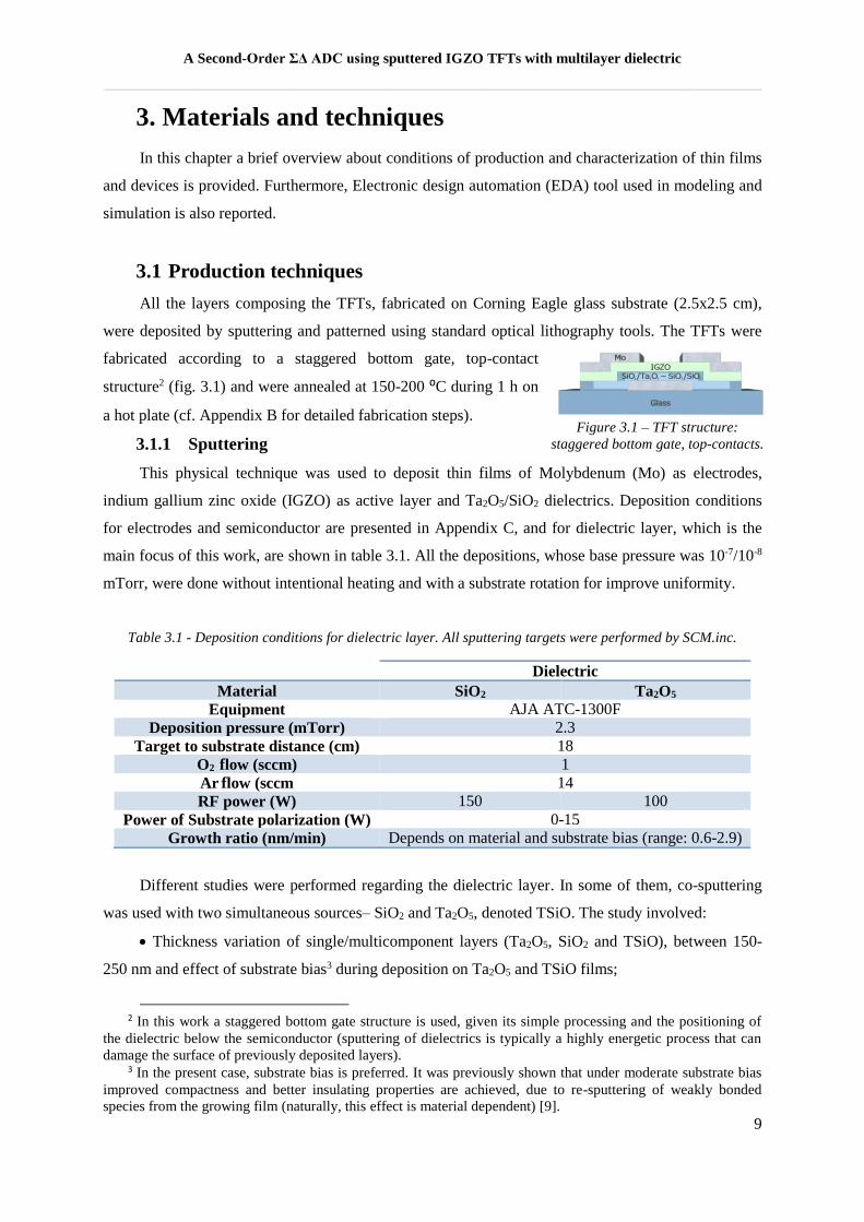
3. Materials and techniques
In this chapter a brief overview about conditions of production and characterization of thin films
and devices is provided. Furthermore, Electronic design automation (EDA) tool used in modeling and
simulation is also reported.
3.1 Production techniques
All the layers composing the TFTs, fabricated on Corning Eagle glass substrate (2.5x2.5 cm),
were deposited by sputtering and patterned using standard optical lithography tools. The TFTs were
fabricated according to a staggered bottom gate, top-contact
structure2 (fig. 3.1) and were annealed at 150-200 ⁰C during 1 h on
a hot plate (cf. Appendix B for detailed fabrication steps).
3.1.1 Sputtering
This physical technique was used to deposit thin films of Molybdenum (Mo) as electrodes,
indium gallium zinc oxide (IGZO) as active layer and Ta2O5/SiO2 dielectrics. Deposition conditions
for electrodes and semiconductor are presented in Appendix C, and for dielectric layer, which is the
main focus of this work, are shown in table 3.1. All the depositions, whose base pressure was 10-7/10-8
mTorr, were done without intentional heating and with a substrate rotation for improve uniformity.
Table 3.1 - Deposition conditions for dielectric layer. All sputtering targets were performed by SCM.inc.
Dielectric
Material SiO2 Ta2O5
Equipment AJA ATC-1300F
Deposition pressure (mTorr) 2.3
Target to substrate distance (cm) 18
O2 flow (sccm) 1
Ar flow (sccm 14
RF power (W) 150 100
Power of Substrate polarization (W) 0-15
Growth ratio (nm/min) Depends on material and substrate bias (range: 0.6-2.9)
Different studies were performed regarding the dielectric layer. In some of them, co-sputtering
was used with two simultaneous sources– SiO2 and Ta2O5, denoted TSiO. The study involved:
Thickness variation of single/multicomponent layers (Ta2O5, SiO2 and TSiO), between 150-
250 nm and effect of substrate bias3 during deposition on Ta2O5 and TSiO films;
2 In this work a staggered bottom gate structure is used, given its simple processing and the positioning of
the dielectric below the semiconductor (sputtering of dielectrics is typically a highly energetic process that can
damage the surface of previously deposited layers). 3 In the present case, substrate bias is preferred. It was previously shown that under moderate substrate bias
improved compactness and better insulating properties are achieved, due to re-sputtering of weakly bonded
species from the growing film (naturally, this effect is material dependent) [9].
Figure 3.1 – TFT structure:
staggered bottom gate, top-contacts.
A Second-Order ΣΔ ADC using sputtered IGZO TFTs with multilayer dielectric
__________________________________________________________________________________
10
Multilayer structures based on TSiO and SiO2 with different number of layers – three (S/T/S)
and seven (S/T/S/T/S/T/S);
Thickness variation of TSiO film when integrated in a multilayer structure (three layers) based
on TSiO and SiO2.
3.1.2 Patterning
After cleaning the substrate4, it was spin-coated with positive photoresist (AZ6612) in a spinner
(Headway Research PWM32), firstly at 3000 rpm during 10 s and then at 4000 rpm during 20 s. After
that, in order to evaporate some solvents and improve photoresist adhesion, dehydration process (soft
baking) was used – substrate was collocated at 115 ⁰C during 1 min and 15 s on a hot plate. Then, it
was necessary to align the substrate with mask5 - mask aligner (Karl Suss MA6) and a UV exposure
process starts in soft-contact mode during 2,5 s. To obtain the desirable pattern, substrate was
introduced in a developer (AZ 726 MIF), controlling the time.
When this process was used in dielectric layer once the photoresist was used as protection in
dry-etching step, the substrate was dipped in acetone, which dissolves the photoresist. A subsequent
cleaning was required.
After thin film deposition, photoresist and thin film deposited on top of it were removed using
acetone, isopropilic alcohol and ultra-pure water (denoted lift-off process). A similar method was used
for resist stripping after dry-etching processes. These were employed solely for the dielectric layers,
using as reactive gas Sulfur hexafluoride (SF6). The used equipment was Alcatel GIR 300, with a base
pressure of 0.05 Pa, gas flow of 10 sccm and an r.f. power of 20 W. The etching rate depends on
material (range: 20-40 nm/min).
3.2 Characterization techniques
The most significant characterization techniques are summarized in table D.1 (cf. Appendix D),
mentioning the main reasons to use them and their most relevant experimental aspects.
3.3 Modeling, Simulation and EDA tools
The TFT model was performed adapting an a-Si TFT model developed by Semiconductor
Devices Research Group at RPI. This model was tested in the software used in this study - Cadence
Design Systems. Furthermore, this software allowed the circuit design and its simulation, using
VirtuosoTM Platform and SpectreTM Simulator from CADENCE. After obtaining an optimized circuit
from an electrical point of view, the layout was done and the files for subsequent mask fabrication
were extracted, using design rules based on the existing fabrication processes available at CENIMAT.
4 Cleaning in ultrasonic bath (acetone followed by isopropilic alcohol); 5 In all steps, negative masks were used to do lift-off, except in dry-etching proceeding which required a
positive mask.
A Second-Order ΣΔ ADC using sputtered IGZO TFTs with multilayer dielectric
__________________________________________________________________________________
11
4. Results and Discussion
Oxide thin-film transistors (TFTs) optimization is essential in order to simulate and produce
complex circuits with them, for instance an analog-to-digital converter (ADC). In fact, some
parameters such as turn-on voltage6 (Von) or even gate leakage current (IG) can affect dramatically
circuit characteristics. These parameters are greatly affected by the properties of the dielectric layer
and its interface with the semiconductor. Therefore, amorphous high-κ dielectrics acquire an important
role, especially in multicomponent and/or multilayer structures, where materials with different
electrical properties (e.g., high-κ and high-EG) are combined to obtain dielectrics with the best possible
performance and reliability [30, 33].
This chapter discusses the results regarding the characterization of dielectric layers, electrical
characterization of TFTs and results concerning the designed sigma delta modulator (ΣΔM) ADC. The
present chapter is divided in three main sections; the first one is dedicated to material characterization
that comprises a detailed analysis about sputtered amorphous multicomponent high-κ dielectrics based
on tantalum pentoxide (Ta2O5) and silicon dioxide (SiO2), using single and multilayer structures, and
their integration in indium gallium zinc oxide (IGZO) TFTs; to finalize the first section, an existing
model for a-Si:H TFTs is adapted to IGZO TFT technology; in the second section, the emphasis is
given to the comparator and the ΣΔM, where their simulation results using IGZO TFT model are
described; the third section is dedicated to the complete layout of the ΣΔM.
4.1 Amorphous multicomponent high-κ dielectrics based on Ta2O5 and
SiO2: thin films and integration in IGZO TFTs
Ta2O5 has been widely used in electronics area, not only in capacitors but also in TFTs. In fact,
when compared with other sputtered dielectrics, Ta2O5 has the advantage of combining a high-κ with
some advantages such as high sputtering rate. As expected, adding SiO2, the co-sputtered material
(Ta2O5-SiO2, denoted TSiO) presents an even higher sputtering rate than isolated Ta2O5 or SiO2 targets.
Indeed, deposition rates for TSiO are 2.5 and 2.9 nm/min, depending if substrate bias is used or not,
while for SiO2 the values obtained are 0.6 and 0.8 nm/min. For Ta2O5, the substrate bias has not any
influence in deposition rate which is, approximately, 1.9 nm/min.
4.1.1 Single layer structure using Ta2O5 and TSiO
Firstly, in this section, two thin films of Ta2O5 and TSiO on Si deposited by sputtering using
substrate bias (see production conditions in Chapter 3) are analyzed. After the thin films analysis, the
integration of these materials in TFTs is evaluated.
6 In TFTs it is usual to use the concept of Von rather than VT to have less ambiguity in defining the onset of
drain-to-source electrical conduction. Von is defined as the VGS value where IDS starts to increase sharply, as seen
in a transfer characteristic in semi-log scale [12].
A Second-Order ΣΔ ADC using sputtered IGZO TFTs with multilayer dielectric
__________________________________________________________________________________
12
For application in TFTs, amorphous structure of the dielectric layer is extremely relevant
because it allows having a good interface with the semiconductor, typically resulting in lower IG,
lower threshold voltage (VT) and higher channel mobility. Although the experimental work on TFTs in
this work is limited to 200 ⁰C (in order to assure compatibility with a large range of plastic substrates),
X-ray Diffraction (XRD) analysis of the fabricated dielectrics annealed at higher temperatures allows
for a better understanding of the studied materials systems, defining for which range of temperatures
they can preserve the amorphous structure.
Both thin films were analyzed between 100 and 900 ⁰C with temperature steps of 100 ⁰C and
doing 3 consecutive scans at each temperature step. In fig. 4.1, the structural data obtained for these
films is shown (curves are presented in steps of 200 ⁰C to simplify the analysis7). As expected for
these dielectrics, only a very broad peak near 2θ=25 ⁰ is visible confirming the amorphous structure of
both materials. For Ta2O5, fig. 4.1a, some peaks start to appear at 700 ⁰C and at 900 ⁰C these peaks are
more pronounced, being attributed to β-Ta2O5. In the inset of this figure, the three consecutives scans
for 700 ⁰C are shown which allow confirming that the crystallization starts at this temperature by
seeing the increase of the intensity of the peaks in each scan. For TSiO, fig. 4.1b, it would be
predictable a higher crystallization temperature due to incorporation of SiO2 – mixing these materials a
structural disorder is induced and, in fact, crystallization only occurs at 900 ⁰C. Both crystallization
temperatures are higher than the limitation considered in this work, meaning that amorphous structure
is conserved for all the fabricated TFTs.
The amorphous structure was confirmed using Atomic Force Microscopy (AFM), as shown in
fig. 4.2. It is possible to note that surfaces of both thin films are completely smooth and their
roughness very low (close to detection limit of equipment, above 0.1 nm).
An elemental analysis of TSiO thin film was done using Rutherford Backscattering
Spectrometry (RBS) technique in Nuclear and Technological Institute (ITN), Portugal. The results
7 In both dielectrics a peak at 2θ=46 ⁰ is visible and is due to the Pt foil (the heating element) above which
the sample is placed.
(b) (a)
Figure 4.1 –Diffractogram for Ta2O5 (a) and TSiO (b) thin films, annealed at different temperatures until the
crystallization is evident. The data obtained is compared with the ICSD database and corresponds to
orthorhombic β- Ta2O5 (ICSD: 98-004-8854).
A Second-Order ΣΔ ADC using sputtered IGZO TFTs with multilayer dielectric
__________________________________________________________________________________
13
(a) (b)
Figure 4.2 - AFM analysis, showing the amorphous structures of Ta2O5 and TSiO thin films.
obtained were fitted, fixing the oxides composition and allowing the system to adjust the
stoichiometry (Ta2O5)x(SiO2)y. According to the results, the thin film presents a Ta2O5/SiO2 ratio of
2.2 and an areal density of 1.4×10¹⁸ at/cm2. The thin film thickness measured by profilometer was 225
nm, which means that considering the thickness obtained by RBS, the co-sputtered material presents a
density near 6.2×10²² at/cm3. Considering the molar mass (441.9 g/mol), the density of β-Ta2O5 (8.2
g/cm3) and the number of atoms presents in each molecule of Ta2O5 (7 atoms), the density of Ta2O5 is
7.8×10²² at/cm3. The density obtained for the TSiO film shows a good match to the theoretical density
of Ta2O5, suggesting a structure with good compactness.
The spectroscopic ellipsometry technique acquires a high importance in dielectrics study. Thin
films of Ta2O5 and TSiO on Si were analyzed using it. The Tauc-Lorentz dispersion formula was used
and the best fitting results were obtained for two oscillators, wherein the range of detection of one of
them was greater than 6 eV. In fig. 4.3, dependences of refractive index (n) and extinction coefficient
(k) on Energy (E) are shown and, in table 4.1, some properties obtained by Tauc-Lorentz dispersion
formula are presented.
(a) (b)
Figure 4.3 - Spectroscopic ellipsometry analysis: comparison between Ta2O5 and TSiO thin films in terms of
refractive index (a) and extinction coefficient (b) with SiO2, as reference.
A Second-Order ΣΔ ADC using sputtered IGZO TFTs with multilayer dielectric
__________________________________________________________________________________
14
Table 4.1 - Properties of Ta2O5 and TSiO films obtained by Tauc-Lorentz dispersion method.
Sample Thickness (nm) Roughness (nm) Eg (eV)
Ta2O5 267.4 1.1 4.20
TSiO 237.7 0.4 4.23
The positioning of the TSiO plots in fig. 4.3 clearly suggests that SiO2 is incorporated in TSiO,
although the Ta2O5 concentration is considerably higher (TSiO plot closer to Ta2O5 in terms of values
and shape). These results are in agreement with RBS analysis, as shown before. It is noteworthy that
due to the usage of substrate bias during thin film deposition, the percentage of SiO2 in film is lower
[9]. Furthermore, the broad peak in n-E plot suggests that samples have an amorphous structure, what
is in agreement with previous results of XRD and AFM. In terms of relative density, the refractive
index for TSiO is lower indicating that its density is lower comparing to Ta2O5, which is consistent
with RBS analysis. Regarding values of energy that induce absorption in the beginning of conduction
band, these are shown in fig. 4.3b. Band gap (Eg) is slightly higher for TSiO than for Ta2O5 film,
suggesting that SiO2 is present in film, but in low percentage. On the other hand, the Eg value even for
Ta2O5 is lower than the typical that is closed to 4.5 eV, which is probably due to sputtering system
(mainly by the usage of substrate bias that induces some differences in film). Other reason found in
literature is related to the model used in simulation which considers the tail-states that are inside the Eg
[9]. In terms of roughness, the values obtained indicate a flat surface in accordance with AFM images.
Given that the main intent of integrating these dielectrics in TFT structures, it is imperative to
analyze several electrical parameters such as κ, breakdown field (EB), capacitance per unit area (Ci)
and current density (J). For this end, metal-insulator-metal (MIM) structures annealed at 150 ⁰C
were analyzed, being the results presented in table 4.28. C-V and C-f plots are shown in fig. E.1
(Appendix E).
Table 4.2 – Electrical properties of Ta2O5 and TSiO determined from MIM structures.
Analyzing the electrical properties of films, it is possible to observe a growth tendency of κ for
dielectrics with higher Ta concentration. In fact, κ obtained for Ta2O5 is extremely close to the values
reported in literature (approximately 25) [56]. TSiO exhibits a higher EB than Ta2O5 which is highly
relevant to improve TFT and circuit reliability. Reinforcing this, J is considerably lower for the co-
sputtering film even with a higher voltage applied.
8 Results for SiO2 films are not presented in this table, given that for the deposition conditions used herein
these films always revealed very large leakage current, inhibiting proper parameter extraction.
Sample Thickness
(nm)
EB
(MV/cm)
κ Ci
(nF/cm2)
J @ EB max
(A/cm2)
Ta2O5 230.0 1.54 22.6 87.0 1.21×10⁻²
TSiO 210.0 2.81 17.0 71.7 8.88×10⁻⁵
A Second-Order ΣΔ ADC using sputtered IGZO TFTs with multilayer dielectric
__________________________________________________________________________________
15
(a) (b)
Figure 4.4 - Measured I-V characteristics for devices with W/L=160/20µm/µm and annealed at 200 ⁰C. Effect of
dielectric composition and the usage of substrate bias in devices with approximately the same thickness (a) and
of dielectrics thicknesses considering the same material and the usage of substrate bias(b).
Next step was to integrate these dielectrics in IGZO TFTs. To this end, TFTs with a staggered
bottom gate, top-contact configuration were produced using Ta2O5 and TSiO as dielectrics. Several
devices were fabricated varying the dielectric thickness, the usage of substrate bias (with or without
substrate bias denoted SB and NSB, respectively) and the annealing temperature (150 or 200 ⁰C)9
Measurement of output and transfer characteristics (static current-voltage) allows acquiring a
comprehensive characterization of a TFT. Output characteristics mostly provide a qualitative
evaluation, giving information about if saturation is achieved (highly relevant for circuit application)
or if there is a significant contact resistance. Transfer characteristics generally provide a more
quantitative analysis, making possible to extract important parameters such as on-off ratio, Von,
subthreshold swing (S) and saturation mobility (µsat) [57].
Fig. 4.4a shows the difference in TFT performance taking into account the two dielectrics
previously analyzed and the influence of using substrate bias during deposition. Fig. 4.4b presents the
influence of dielectric thicknesses on the TFT’s transfer characteristics, considering the amplitude of
gate leakage current (IG). The electrical properties of devices depicted in fig. 4.4 are summarized in
table 4.3. The µsat was calculated in the saturation regime. An output curve for one representative
device of this batch is shown in Fig. E.2, Appendix E, being observed that the contact resistance does
not have a significant influence in TFT performance considering this channel length (L), the interface
IGZO/ Mo and the annealing temperature.
For TFTs with Ta2O5 dielectric a large increase of off-current (which also detrimentally affects
S) is verified for lower dielectric thickness and NSB condition, proving the importance of these
parameters to achieve good performance devices. Nevertheless, note that regardless of the processing
conditions, Ta2O5-based transistors always present a large variation of properties over a substrate, as
shown in Appendix E. In general, TFTs with TSiO present enhanced properties, particularly a closer to
0 V Von and improved uniformity (in terms of device-to-device variation in the same substrate). Again,
9 Influence of annealing temperature will be analyzed in section 4.1.2.
A Second-Order ΣΔ ADC using sputtered IGZO TFTs with multilayer dielectric
__________________________________________________________________________________
16
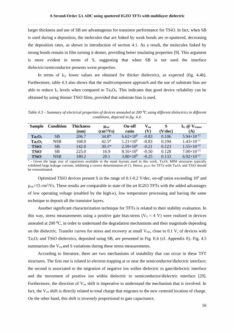
larger thickness and use of SB are advantageous for transistor performance for TSiO. In fact, when SB
is used during a deposition, the molecules that are linked by weak bonds are re-sputtered, decreasing
the deposition rates, as shown in introduction of section 4.1. As a result, the molecules linked by
strong bonds remain in film turning it denser, providing better insulating properties [9]. This argument
is more evident in terms of S, suggesting that when SB is not used the interface
dielectric/semiconductor presents worst properties.
In terms of IG, lower values are obtained for thicker dielectrics, as expected (fig. 4.4b).
Furthermore, table 4.3 also shows that the multicomponent approach and the use of substrate bias are
able to reduce IG levels when compared to Ta2O5. This indicates that good device reliability can be
obtained by using thinner TSiO films, provided that substrate bias is used.
Table 4.3 – Summary of electrical properties of devices annealed at 200 ⁰C using different dielectrics in different
conditions, depicted in fig. 4.4.
Sample Condition Thickness
(nm)
µsat
(cm2/Vs)
On-off
ratio
Von
(V)
S
(V/dec)
IG @ VGmax
(A)
Ta2O5 SB 206.7 34.8* 6.62×108 -0.83 0.106 5.94×10⁻¹² Ta2O5 NSB 168.0 42.5* 1.21×106 -0.83 0.194 1.43×10⁻¹¹
TSiO SB 142.0 30.1* 2.59×108 -0.21 0.123 1.55×10⁻¹²
TSiO SB 225.0 16.9 8.16×10⁸ -0.50 0.128 7.00×10⁻¹³
TSiO NSB 180.2 20.1 3.80×10⁸ -0.25 0.133 6.92×10⁻¹² * - Given the large size of capacitors available in the mask layouts used in this work, Ta2O5 MIM structures typically
exhibited large leakage currents, inhibiting a correct determination of Ci. Hence, µSAT for TFTs with Ta2O5 and TSiO should
be overestimated.
Optimized TSiO devices present S in the range of 0.1-0.2 V/dec, on-off ratios exceeding 108 and
µsat>15 cm2/Vs. These results are comparable to state of the art IGZO TFTs with the added advantages
of low operating voltage (enabled by the high-κ), low temperature processing and having the same
technique to deposit all the transistor layers.
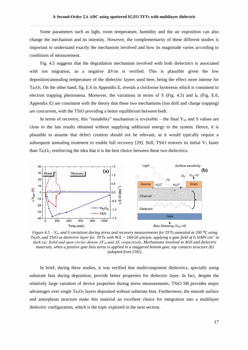
Another significant characterization technique for TFTs is related to their stability evaluation. In
this way, stress measurements using a positive gate bias-stress (VG ≈ 4 V) were realized in devices
annealed at 200 ⁰C, in order to understand the degradation mechanisms and their magnitude depending
on the dielectric. Transfer curves for stress and recovery at small VDS, close to 0.1 V, of devices with
Ta2O5 and TSiO dielectrics, deposited using SB, are presented in Fig. E.6 (cf. Appendix E). Fig. 4.5
summarizes the Von and S variations during these stress measurements.
According to literature, there are two mechanisms of instability that can occur in these TFT
structures. The first one is related to electron trapping at or near the semiconductor/dielectric interface;
the second is associated to the migration of negative ion within dielectric to gate/dielectric interface
and the movement of positive ion within dielectric to semiconductor/dielectric interface [29].
Furthermore, the direction of Von shift is imperative to understand the mechanism that is involved. In
fact, the Von shift is directly related to total charge that migrates to the new centroid location of charge.
On the other hand, this shift is inversely proportional to gate capacitance.
A Second-Order ΣΔ ADC using sputtered IGZO TFTs with multilayer dielectric
__________________________________________________________________________________
17
Figure 4.5 – Von and S variations during stress and recovery measurements for TFTs annealed at 200 ⁰C using
Ta2O5 and TSiO as dielectric layer for TFTs with W/L = 160/20 µm/µm, applying a gate field of 0.16MV.cm-1 in
dark (a). Solid and open circles denote ΔVon and ΔS, respectively. Mechanisms involved in AOS and dielectric
materials, when a positive gate bias stress is applied in a staggered bottom gate, top contacts structure (b)
(adapted from [58]).
(a) (b)
Some parameters such as light, room temperature, humidity and the air exposition can also
change the mechanism and its intensity. However, the complementarity of these different studies is
important to understand exactly the mechanism involved and how its magnitude varies according to
conditions of measurement. [27]
Fig. 4.5 suggests that the degradation mechanism involved with both dielectrics is associated
with ion migration, as a negative ∆Von is verified. This is plausible given the low
deposition/annealing temperature of the dielectric layers used here, being the effect more intense for
Ta2O5. On the other hand, fig. E.6 in Appendix E, reveals a clockwise hysteresis which is consistent to
electron trapping phenomena. Moreover, the variations in terms of S (Fig. 4.5) and ID (Fig. E.6,
Appendix E) are consistent with the theory that these two mechanisms (ion drift and charge trapping)
are concurrent, with the TSiO providing a better equilibrium between both.
In terms of recovery, this “instability” mechanism is reversible – the final Von and S values are
close to the last results obtained without supplying additional energy to the system. Hence, it is
plausible to assume that defect creation should not be relevant, as it would typically require a
subsequent annealing treatment to enable full recovery [29]. Still, TSiO restores its initial VT faster
than Ta2O5, reinforcing the idea that it is the best choice between these two dielectrics. [58]
In brief, during these studies, it was verified that multicomponent dielectrics, specially using
substrate bias during deposition, provide better properties for dielectric layer. In fact, despite the
relatively large variation of device properties during stress measurements, TSiO SB provides major
advantages over single Ta2O5 layers deposited without substrate bias. Furthermore, the smooth surface
and amorphous structure make this material an excellent choice for integration into a multilayer
dielectric configuration, which is the topic explored in the next section.
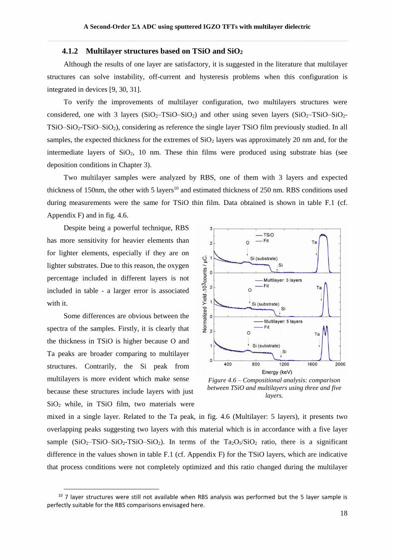
A Second-Order ΣΔ ADC using sputtered IGZO TFTs with multilayer dielectric
__________________________________________________________________________________
18
Figure 4.6 – Compositional analysis: comparison
between TSiO and multilayers using three and five
layers.
4.1.2 Multilayer structures based on TSiO and SiO2
Although the results of one layer are satisfactory, it is suggested in the literature that multilayer
structures can solve instability, off-current and hysteresis problems when this configuration is
integrated in devices [9, 30, 31].
To verify the improvements of multilayer configuration, two multilayers structures were
considered, one with 3 layers (SiO2–TSiO–SiO2) and other using seven layers (SiO2–TSiO–SiO2-
TSiO–SiO2-TSiO–SiO2), considering as reference the single layer TSiO film previously studied. In all
samples, the expected thickness for the extremes of SiO2 layers was approximately 20 nm and, for the
intermediate layers of SiO2, 10 nm. These thin films were produced using substrate bias (see
deposition conditions in Chapter 3).
Two multilayer samples were analyzed by RBS, one of them with 3 layers and expected
thickness of 150nm, the other with 5 layers10 and estimated thickness of 250 nm. RBS conditions used
during measurements were the same for TSiO thin film. Data obtained is shown in table F.1 (cf.
Appendix F) and in fig. 4.6.
Despite being a powerful technique, RBS
has more sensitivity for heavier elements than
for lighter elements, especially if they are on
lighter substrates. Due to this reason, the oxygen
percentage included in different layers is not
included in table - a larger error is associated
with it.
Some differences are obvious between the
spectra of the samples. Firstly, it is clearly that
the thickness in TSiO is higher because O and
Ta peaks are broader comparing to multilayer
structures. Contrarily, the Si peak from
multilayers is more evident which make sense
because these structures include layers with just
SiO2 while, in TSiO film, two materials were
mixed in a single layer. Related to the Ta peak, in fig. 4.6 (Multilayer: 5 layers), it presents two
overlapping peaks suggesting two layers with this material which is in accordance with a five layer
sample (SiO2–TSiO–SiO2-TSiO–SiO2). In terms of the Ta2O5/SiO2 ratio, there is a significant
difference in the values shown in table F.1 (cf. Appendix F) for the TSiO layers, which are indicative
that process conditions were not completely optimized and this ratio changed during the multilayer
10 7 layer structures were still not available when RBS analysis was performed but the 5 layer sample is
perfectly suitable for the RBS comparisons envisaged here.
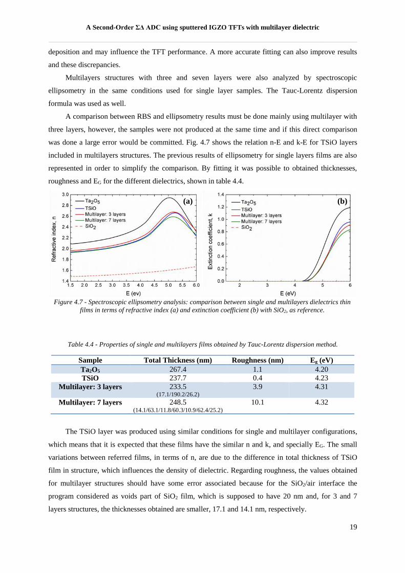
A Second-Order ΣΔ ADC using sputtered IGZO TFTs with multilayer dielectric
__________________________________________________________________________________
19
(a)
Figure 4.7 - Spectroscopic ellipsometry analysis: comparison between single and multilayers dielectrics thin
films in terms of refractive index (a) and extinction coefficient (b) with SiO2, as reference.
(b)
deposition and may influence the TFT performance. A more accurate fitting can also improve results
and these discrepancies.
Multilayers structures with three and seven layers were also analyzed by spectroscopic
ellipsometry in the same conditions used for single layer samples. The Tauc-Lorentz dispersion
formula was used as well.
A comparison between RBS and ellipsometry results must be done mainly using multilayer with
three layers, however, the samples were not produced at the same time and if this direct comparison
was done a large error would be committed. Fig. 4.7 shows the relation n-E and k-E for TSiO layers
included in multilayers structures. The previous results of ellipsometry for single layers films are also
represented in order to simplify the comparison. By fitting it was possible to obtained thicknesses,
roughness and EG for the different dielectrics, shown in table 4.4.
Table 4.4 - Properties of single and multilayers films obtained by Tauc-Lorentz dispersion method.
Sample Total Thickness (nm) Roughness (nm) Eg (eV)
Ta2O5 267.4 1.1 4.20
TSiO 237.7 0.4 4.23
Multilayer: 3 layers 233.5 (17.1/190.2/26.2)
3.9 4.31
Multilayer: 7 layers 248.5 (14.1/63.1/11.8/60.3/10.9/62.4/25.2)
10.1 4.32
The TSiO layer was produced using similar conditions for single and multilayer configurations,
which means that it is expected that these films have the similar n and k, and specially EG. The small
variations between referred films, in terms of n, are due to the difference in total thickness of TSiO
film in structure, which influences the density of dielectric. Regarding roughness, the values obtained
for multilayer structures should have some error associated because for the SiO2/air interface the
program considered as voids part of SiO2 film, which is supposed to have 20 nm and, for 3 and 7
layers structures, the thicknesses obtained are smaller, 17.1 and 14.1 nm, respectively.
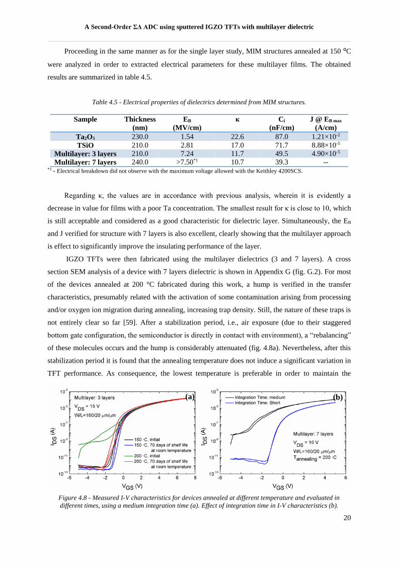
A Second-Order ΣΔ ADC using sputtered IGZO TFTs with multilayer dielectric
__________________________________________________________________________________
20
Figure 4.8 - Measured I-V characteristics for devices annealed at different temperature and evaluated in
different times, using a medium integration time (a). Effect of integration time in I-V characteristics (b).
(a) (b)
Proceeding in the same manner as for the single layer study, MIM structures annealed at 150 ⁰C
were analyzed in order to extracted electrical parameters for these multilayer films. The obtained
results are summarized in table 4.5.
Table 4.5 - Electrical properties of dielectrics determined from MIM structures.
*1 - Electrical breakdown did not observe with the maximum voltage allowed with the Keithley 4200SCS.
Regarding κ, the values are in accordance with previous analysis, wherein it is evidently a
decrease in value for films with a poor Ta concentration. The smallest result for κ is close to 10, which
is still acceptable and considered as a good characteristic for dielectric layer. Simultaneously, the EB
and J verified for structure with 7 layers is also excellent, clearly showing that the multilayer approach
is effect to significantly improve the insulating performance of the layer.
IGZO TFTs were then fabricated using the multilayer dielectrics (3 and 7 layers). A cross
section SEM analysis of a device with 7 layers dielectric is shown in Appendix G (fig. G.2). For most
of the devices annealed at 200 °C fabricated during this work, a hump is verified in the transfer
characteristics, presumably related with the activation of some contamination arising from processing
and/or oxygen ion migration during annealing, increasing trap density. Still, the nature of these traps is
not entirely clear so far [59]. After a stabilization period, i.e., air exposure (due to their staggered
bottom gate configuration, the semiconductor is directly in contact with environment), a “rebalancing”
of these molecules occurs and the hump is considerably attenuated (fig. 4.8a). Nevertheless, after this
stabilization period it is found that the annealing temperature does not induce a significant variation in
TFT performance. As consequence, the lowest temperature is preferable in order to maintain the
Sample Thickness
(nm)
EB
(MV/cm)
κ Ci
(nF/cm)
J @ EB max
(A/cm)
Ta2O5 230.0 1.54 22.6 87.0 1.21×10⁻²
TSiO 210.0 2.81 17.0 71.7 8.88×10⁻⁵
Multilayer: 3 layers 210.0 7.24 11.7 49.5 4.90×10⁻⁵
Multilayer: 7 layers 240.0 >7.50*1 10.7 39.3 --
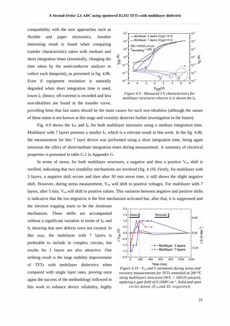
A Second-Order ΣΔ ADC using sputtered IGZO TFTs with multilayer dielectric
__________________________________________________________________________________
21
Figure 4.9 - Measured I-V characteristics for
multilayer structures wherein it is shown the IG.
Figure 4.10 - Von and S variations during stress and
recovery measurements for TFTs annealed at 200 ⁰C
using multilayers structures (W/L = 160/20 µm/µm),
applying a gate field of 0.16MV.cm-1. Solid and open
circles denote ΔVon and ΔS, respectively.
compatibility with the new approaches such as
flexible and paper electronics. Another
interesting result is found when comparing
transfer characteristics taken with medium and
short integration times (essentially, changing the
time taken by the semiconductor analyzer to
collect each datapoint), as presented in fig. 4.8b.
Even if equipment resolution is naturally
degraded when short integration time is used,
lower IG (hence, off-current) is recorded and less
non-idealities are found in the transfer curve,
providing hints that fast states should be the main causes for such non-idealities (although the nature
of these states is not known at this stage and certainly deserves further investigation in the future).
Fig. 4.9 shows the IDS and IG for both multilayer structures using a medium integration time.
Multilayer with 7 layers presents a smaller IG, which is a relevant result in this work. In the fig. 4.8b,
the measurement for this 7 layer device was performed using a short integration time, being again
notorious the effect of short/medium integration times during measurement. A summary of electrical
properties is presented in table G.1 in Appendix G.
In terms of stress, for both multilayer structures, a negative and then a positive Von shift is
verified, indicating that two instability mechanisms are involved (fig. 4.10). Firstly, for multilayer with
3 layers, a negative shift occurs and then after 30 min stress time, it still shows the slight negative
shift. However, during stress measurement, Von will shift to positive voltages. For multilayer with 7
layers, after 5 min, Von will shift to positive values. This variation between negative and positive shifts
is indicative that the ion migration is the first mechanism activated but, after that, it is suppressed and
the electron trapping starts to be the dominant
mechanism. These shifts are accompanied
without a significant variation in terms of ID and
S, showing that new defects were not created. In
this way, the multilayer with 7 layers is
preferable to include in complex circuits, but
results for 3 layers are also attractive. One
striking result is the large stability improvement
of TFTs with multilayer dielectrics when
compared with single layer ones, proving once
again the success of the methodology followed in
this work to enhance device reliability, highly
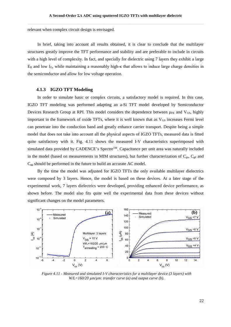
A Second-Order ΣΔ ADC using sputtered IGZO TFTs with multilayer dielectric
__________________________________________________________________________________
22
(a) (b)
Figure 4.11 - Measured and simulated I-V characteristics for a multilayer device (3 layers) with
W/L=160/20 µm/µm: transfer curve (a) and output curve (b).
relevant when complex circuit design is envisaged.
In brief, taking into account all results obtained, it is clear to conclude that the multilayer
structures greatly improve the TFT performance and stability and are preferable to include in circuits
with a high level of complexity. In fact, and specially for dielectric using 7 layers they exhibit a large
EB and low IG, while maintaining a reasonably high-κ that allows to induce large charge densities in
the semiconductor and allow for low voltage operation.
4.1.3 IGZO TFT Modeling
In order to simulate basic or complex circuits, a satisfactory model is required. In this case,
IGZO TFT modeling was performed adapting an a-Si TFT model developed by Semiconductor
Devices Research Group at RPI. This model considers the dependence between µFE and VGS, highly
important in the framework of oxide TFTs, where it is well known that as VGS increases Fermi level
can penetrate into the conduction band and greatly enhance carrier transport. Despite being a simple
model that does not take into account all the physical aspects of IGZO TFTs, measured data is fitted
quite satisfactory with it. Fig. 4.11 shows the measured I-V characteristics superimposed with
simulated data provided by CADENCE’s SpectreTM. Capacitance per unit area was naturally included
in the model (based on measurements in MIM structures), but further characterization of Cgs, Cgd and
Cgg should be performed in the future to build an accurate AC model.
By the time the model was adjusted for IGZO TFTs the only available multilayer dielectrics
were composed by 3 layers. Hence, the model is based on these devices. At a later stage of the
experimental work, 7 layers dielectrics were developed, providing enhanced device performance, as
shown before. The model also fits quite well the experimental data from these devices without
significant changes on the model parameters.
a
)
b
)
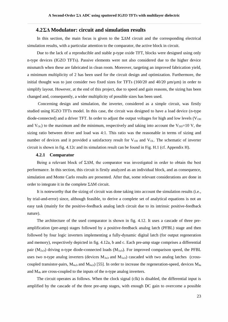
A Second-Order ΣΔ ADC using sputtered IGZO TFTs with multilayer dielectric
__________________________________________________________________________________
23
4.2 ΣΔ Modulator: circuit and simulation results
In this section, the main focus is given to the ΣΔM circuit and the corresponding electrical
simulation results, with a particular attention to the comparator, the active block in circuit.
Due to the lack of a reproducible and stable p-type oxide TFT, blocks were designed using only
n-type devices (IGZO TFTs). Passive elements were not also considered due to the higher device
mismatch when these are fabricated in clean room. Moreover, targeting an improved fabrication yield,
a minimum multiplicity of 2 has been used for the circuit design and optimization. Furthermore, the
initial thought was to just consider two fixed sizes for TFTs (160/20 and 40/20 µm/µm) in order to
simplify layout. However, at the end of this project, due to speed and gain reasons, the sizing has been
changed and, consequently, a wider multiplicity of possible sizes has been used.
Concerning design and simulation, the inverter, considered as a simple circuit, was firstly
studied using IGZO TFTs model. In this case, the circuit was designed to have a load device (n-type
diode-connected) and a driver TFT. In order to adjust the output voltages for high and low levels (VOH
and VOL) to the maximum and the minimum, respectively and taking into account the VDD=10 V, the
sizing ratio between driver and load was 4:1. This ratio was the reasonable in terms of sizing and
number of devices and it provided a satisfactory result for VOH and VOL. The schematic of inverter
circuit is shown in fig. 4.12c and its simulation result can be found in Fig. H.1 (cf. Appendix H).
4.2.1 Comparator
Being a relevant block of ΣΔM, the comparator was investigated in order to obtain the best
performance. In this section, this circuit is firstly analyzed as an individual block, and as consequence,
simulation and Monte Carlo results are presented. After that, some relevant considerations are done in
order to integrate it in the complete ΣΔM circuit.
It is noteworthy that the sizing of circuit was done taking into account the simulation results (i.e.,
by trial-and-error) since, although feasible, to derive a complete set of analytical equations is not an
easy task (mainly for the positive-feedback analog latch circuit due to its intrinsic positive-feedback
nature).
The architecture of the used comparator is shown in fig. 4.12. It uses a cascade of three pre-
amplification (pre-amp) stages followed by a positive-feedback analog latch (PFBL) stage and then
followed by four logic inverters implementing a fully-dynamic digital latch (for output regeneration
and memory), respectively depicted in fig. 4.12a, b and c. Each pre-amp stage comprises a differential
pair (M2a,b) driving n-type diode-connected loads (M1a,b). For improved comparison speed, the PFBL
uses two n-type analog inverters (devices M3a,b and M5a,b) cascaded with two analog latches (cross-
coupled transistor-pairs, M4a,b and M6a,b) [55]. In order to increase the regeneration-speed, devices M4a
and M4b are cross-coupled to the inputs of the n-type analog inverters.
The circuit operates as follows. When the clock signal (clk) is disabled, the differential input is
amplified by the cascade of the three pre-amp stages, with enough DC gain to overcome a possible
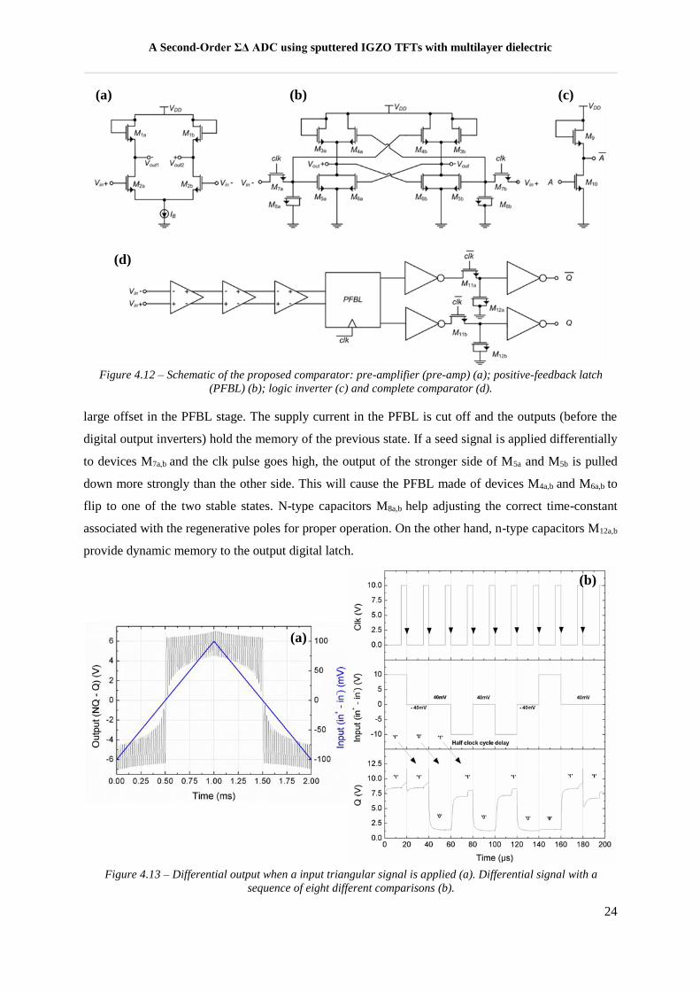
A Second-Order ΣΔ ADC using sputtered IGZO TFTs with multilayer dielectric
__________________________________________________________________________________
24
Figure 4.12 – Schematic of the proposed comparator: pre-amplifier (pre-amp) (a); positive-feedback latch
(PFBL) (b); logic inverter (c) and complete comparator (d).
(a)
(d)
(b) (c)
large offset in the PFBL stage. The supply current in the PFBL is cut off and the outputs (before the
digital output inverters) hold the memory of the previous state. If a seed signal is applied differentially
to devices M7a,b and the clk pulse goes high, the output of the stronger side of M5a and M5b is pulled
down more strongly than the other side. This will cause the PFBL made of devices M4a,b and M6a,b to
flip to one of the two stable states. N-type capacitors M8a,b help adjusting the correct time-constant
associated with the regenerative poles for proper operation. On the other hand, n-type capacitors M12a,b
provide dynamic memory to the output digital latch.
(a)
(b)
Figure 4.13 – Differential output when a input triangular signal is applied (a). Differential signal with a
sequence of eight different comparisons (b).
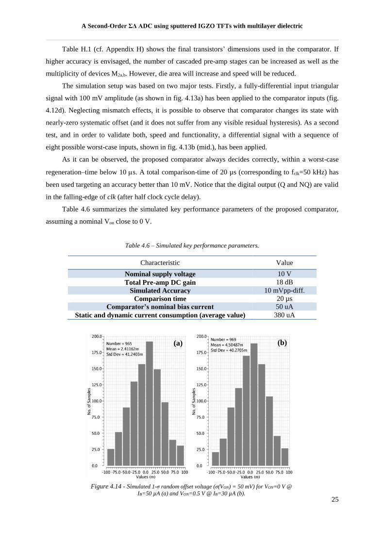
A Second-Order ΣΔ ADC using sputtered IGZO TFTs with multilayer dielectric
__________________________________________________________________________________
25
Table H.1 (cf. Appendix H) shows the final transistors’ dimensions used in the comparator. If
higher accuracy is envisaged, the number of cascaded pre-amp stages can be increased as well as the
multiplicity of devices M2a,b. However, die area will increase and speed will be reduced.
The simulation setup was based on two major tests. Firstly, a fully-differential input triangular
signal with 100 mV amplitude (as shown in fig. 4.13a) has been applied to the comparator inputs (fig.
4.12d). Neglecting mismatch effects, it is possible to observe that comparator changes its state with
nearly-zero systematic offset (and it does not suffer from any visible residual hysteresis). As a second
test, and in order to validate both, speed and functionality, a differential signal with a sequence of
eight possible worst-case inputs, shown in fig. 4.13b (mid.), has been applied.
As it can be observed, the proposed comparator always decides correctly, within a worst-case
regeneration–time below 10 s. A total comparison-time of 20 µs (corresponding to fclk=50 kHz) has
been used targeting an accuracy better than 10 mV. Notice that the digital output (Q and NQ) are valid
in the falling-edge of clk (after half clock cycle delay).
Table 4.6 summarizes the simulated key performance parameters of the proposed comparator,
assuming a nominal Von close to 0 V.
Table 4.6 – Simulated key performance parameters.
Characteristic Value
Nominal supply voltage 10 V
Total Pre-amp DC gain 18 dB
Simulated Accuracy 10 mVpp-diff.
Comparison time 20 µs
Comparator’s nominal bias current 50 uA
Static and dynamic current consumption (average value) 380 uA
(a) (b)
Figure 4.14 - Simulated 1-σ random offset voltage (σ(VON) = 50 mV) for VON=0 V @
IB=50 µA (a) and VON=0.5 V @ IB=30 µA (b).
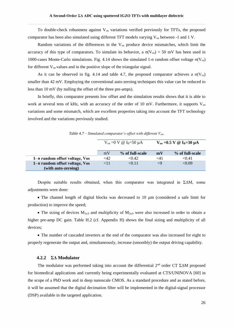
A Second-Order ΣΔ ADC using sputtered IGZO TFTs with multilayer dielectric
__________________________________________________________________________________
26
To double-check robustness against Von variations verified previously for TFTs, the proposed
comparator has been also simulated using different TFT models varying Von between -1 and 1 V.
Random variations of the differences in the Von produce device mismatches, which limit the
accuracy of this type of comparators. To simulate its behavior, a σ(Von) = 50 mV has been used in
1000-cases Monte-Carlo simulations. Fig. 4.14 shows the simulated 1-σ random offset voltage σ(Vos)
for different Von values and in the positive slope of the triangular signal.
As it can be observed in fig. 4.14 and table 4.7, the proposed comparator achieves a σ(Vos)
smaller than 42 mV. Employing the conventional auto-zeroing techniques this value can be reduced to
less than 10 mV (by nulling the offset of the three pre-amps).
In briefly, this comparator presents low offset and the simulation results shows that it is able to
work at several tens of kHz, with an accuracy of the order of 10 mV. Furthermore, it supports Von
variations and some mismatch, which are excellent properties taking into account the TFT technology
involved and the variations previously studied.
Table 4.7 – Simulated comparator’s offset with different Von.
Von =0 V @ IB=50 µA Von =0.5 V @ IB=30 µA
mV % of full-scale mV % of full-scale
1- σ random offset voltage, Vos <42 <0.42 <41 <0.41
1- σ random offset voltage, Vos
(with auto-zeroing)
<11 <0.11 <9 <0.09
Despite suitable results obtained, when this comparator was integrated in ΣΔM, some
adjustments were done:
The channel length of digital blocks was decreased to 10 µm (considered a safe limit for
production) to improve the speed;
The sizing of devices M1a,b and multiplicity of M2a,b were also increased in order to obtain a
higher pre-amp DC gain. Table H.2 (cf. Appendix H) shows the final sizing and multiplicity of all
devices;
The number of cascaded inverters at the end of the comparator was also increased for eight to
properly regenerate the output and, simultaneously, increase (smoothly) the output driving capability.
4.2.2 ΣΔ Modulator
The modulator was performed taking into account the differential 2nd order CT ΣΔM proposed
for biomedical applications and currently being experimentally evaluated at CTS/UNINOVA [60] in
the scope of a PhD work and in deep nanoscale CMOS. As a standard procedure and as stated before,
it will be assumed that the digital decimation filter will be implemented in the digital-signal processor
(DSP) available in the targeted application.
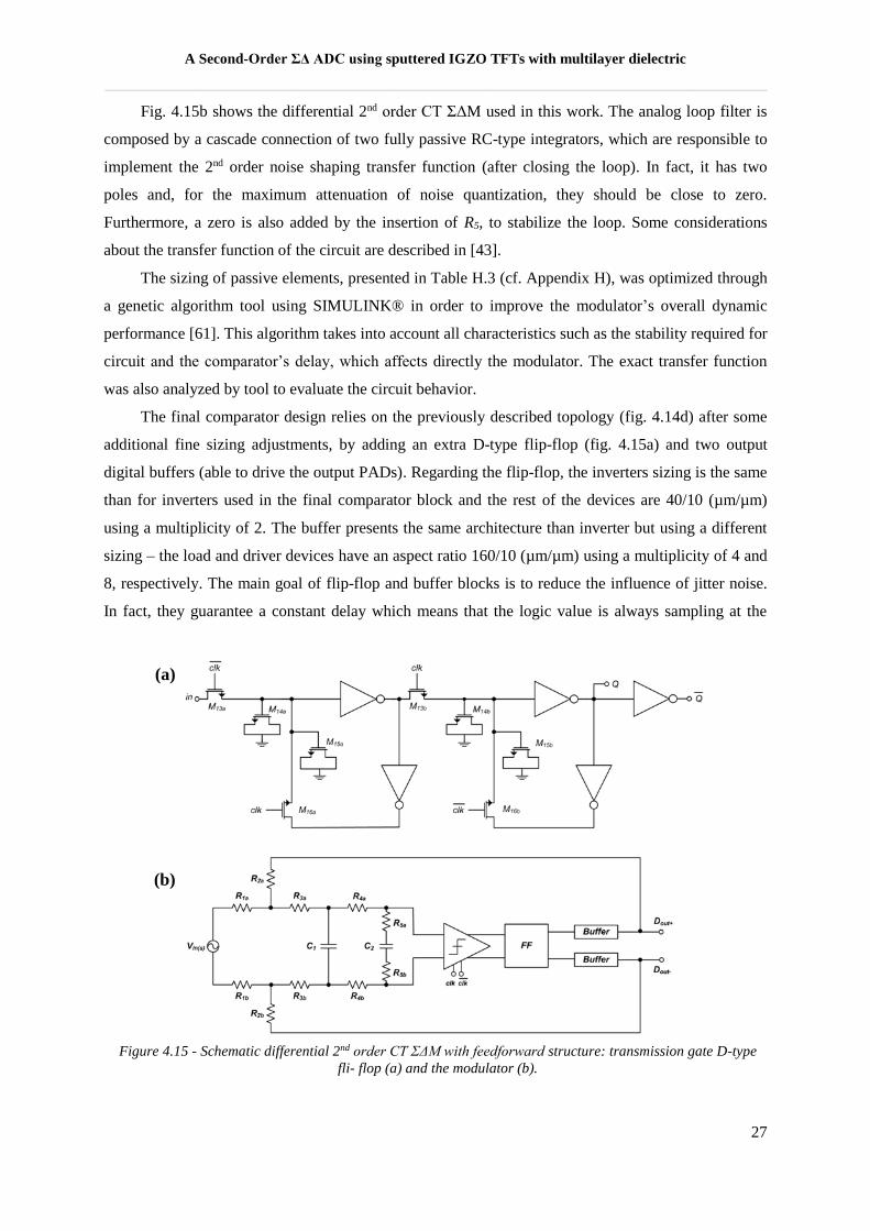
A Second-Order ΣΔ ADC using sputtered IGZO TFTs with multilayer dielectric
__________________________________________________________________________________
27
(a)
(b)
Figure 4.15 - Schematic differential 2nd order CT ΣΔM with feedforward structure: transmission gate D-type
fli- flop (a) and the modulator (b).
Fig. 4.15b shows the differential 2nd order CT ΣΔM used in this work. The analog loop filter is
composed by a cascade connection of two fully passive RC-type integrators, which are responsible to
implement the 2nd order noise shaping transfer function (after closing the loop). In fact, it has two
poles and, for the maximum attenuation of noise quantization, they should be close to zero.
Furthermore, a zero is also added by the insertion of R5, to stabilize the loop. Some considerations
about the transfer function of the circuit are described in [43].
The sizing of passive elements, presented in Table H.3 (cf. Appendix H), was optimized through
a genetic algorithm tool using SIMULINK® in order to improve the modulator’s overall dynamic
performance [61]. This algorithm takes into account all characteristics such as the stability required for
circuit and the comparator’s delay, which affects directly the modulator. The exact transfer function
was also analyzed by tool to evaluate the circuit behavior.
The final comparator design relies on the previously described topology (fig. 4.14d) after some
additional fine sizing adjustments, by adding an extra D-type flip-flop (fig. 4.15a) and two output
digital buffers (able to drive the output PADs). Regarding the flip-flop, the inverters sizing is the same
than for inverters used in the final comparator block and the rest of the devices are 40/10 (µm/µm)
using a multiplicity of 2. The buffer presents the same architecture than inverter but using a different
sizing – the load and driver devices have an aspect ratio 160/10 (µm/µm) using a multiplicity of 4 and
8, respectively. The main goal of flip-flop and buffer blocks is to reduce the influence of jitter noise.
In fact, they guarantee a constant delay which means that the logic value is always sampling at the
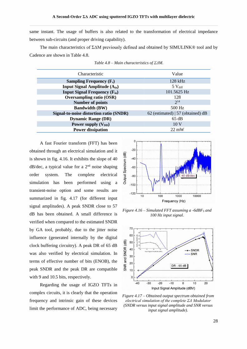
A Second-Order ΣΔ ADC using sputtered IGZO TFTs with multilayer dielectric
__________________________________________________________________________________
28
Figure 4.17 – Obtained output spectrum obtained from
electrical simulation of the complete ΣΔ Modulator
(SNDR versus input signal amplitude and SNR versus
input signal amplitude).
same instant. The usage of buffers is also related to the transformation of electrical impedance
between sub-circuits (and proper driving capability).
The main characteristics of ΣΔM previously defined and obtained by SIMULINK® tool and by
Cadence are shown in Table 4.8.
Table 4.8 – Main characteristics of ΣΔM.
Characteristic Value
Sampling Frequency (Fs) 128 kHz
Input Signal Amplitude (Ain) 5 Vdiff
Input Signal Frequency (Fin) 101.5625 Hz
Oversampling ratio (OSR) 128
Number of points 214
Bandwidth (BW) 500 Hz
Signal-to-noise distortion ratio (SNDR) 62 (estimated) | 57 (obtained) dB
Dynamic Range (DR) 65 dB
Power supply (VDD) 10 V
Power dissipation 22 mW
A fast Fourier transform (FFT) has been
obtained through an electrical simulation and it
is shown in fig. 4.16. It exhibits the slope of 40
dB/dec, a typical value for a 2nd noise shaping
order system. The complete electrical
simulation has been performed using a
transient-noise option and some results are
summarized in fig. 4.17 (for different input
signal amplitudes). A peak SNDR close to 57
dB has been obtained. A small difference is
verified when compared to the estimated SNDR
by GA tool, probably, due to the jitter noise
influence (generated internally by the digital
clock buffering circuitry). A peak DR of 65 dB
was also verified by electrical simulation. In
terms of effective number of bits (ENOB), the
peak SNDR and the peak DR are compatible
with 9 and 10.5 bits, respectively.
Regarding the usage of IGZO TFTs in
complex circuits, it is clearly that the operation
frequency and intrinsic gain of these devices
limit the performance of ADC, being necessary
Figure 4.16 – Simulated FFT assuming a -6dBFS and
100 Hz input signal.
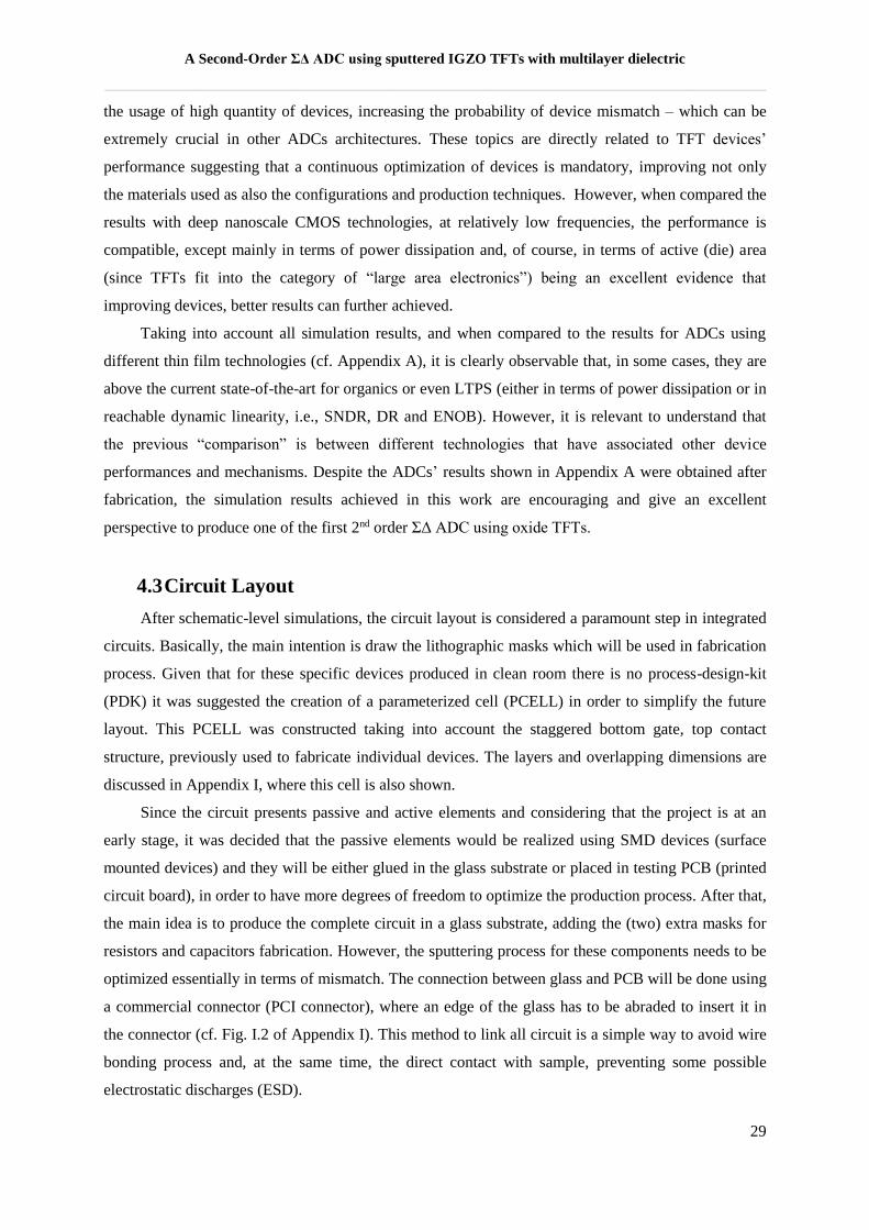
A Second-Order ΣΔ ADC using sputtered IGZO TFTs with multilayer dielectric
__________________________________________________________________________________
29
the usage of high quantity of devices, increasing the probability of device mismatch – which can be
extremely crucial in other ADCs architectures. These topics are directly related to TFT devices’
performance suggesting that a continuous optimization of devices is mandatory, improving not only
the materials used as also the configurations and production techniques. However, when compared the
results with deep nanoscale CMOS technologies, at relatively low frequencies, the performance is
compatible, except mainly in terms of power dissipation and, of course, in terms of active (die) area
(since TFTs fit into the category of “large area electronics”) being an excellent evidence that
improving devices, better results can further achieved.
Taking into account all simulation results, and when compared to the results for ADCs using
different thin film technologies (cf. Appendix A), it is clearly observable that, in some cases, they are
above the current state-of-the-art for organics or even LTPS (either in terms of power dissipation or in
reachable dynamic linearity, i.e., SNDR, DR and ENOB). However, it is relevant to understand that
the previous “comparison” is between different technologies that have associated other device
performances and mechanisms. Despite the ADCs’ results shown in Appendix A were obtained after
fabrication, the simulation results achieved in this work are encouraging and give an excellent
perspective to produce one of the first 2nd order ΣΔ ADC using oxide TFTs.
4.3 Circuit Layout
After schematic-level simulations, the circuit layout is considered a paramount step in integrated
circuits. Basically, the main intention is draw the lithographic masks which will be used in fabrication
process. Given that for these specific devices produced in clean room there is no process-design-kit
(PDK) it was suggested the creation of a parameterized cell (PCELL) in order to simplify the future
layout. This PCELL was constructed taking into account the staggered bottom gate, top contact
structure, previously used to fabricate individual devices. The layers and overlapping dimensions are
discussed in Appendix I, where this cell is also shown.
Since the circuit presents passive and active elements and considering that the project is at an
early stage, it was decided that the passive elements would be realized using SMD devices (surface
mounted devices) and they will be either glued in the glass substrate or placed in testing PCB (printed
circuit board), in order to have more degrees of freedom to optimize the production process. After that,
the main idea is to produce the complete circuit in a glass substrate, adding the (two) extra masks for
resistors and capacitors fabrication. However, the sputtering process for these components needs to be
optimized essentially in terms of mismatch. The connection between glass and PCB will be done using
a commercial connector (PCI connector), where an edge of the glass has to be abraded to insert it in
the connector (cf. Fig. I.2 of Appendix I). This method to link all circuit is a simple way to avoid wire
bonding process and, at the same time, the direct contact with sample, preventing some possible
electrostatic discharges (ESD).
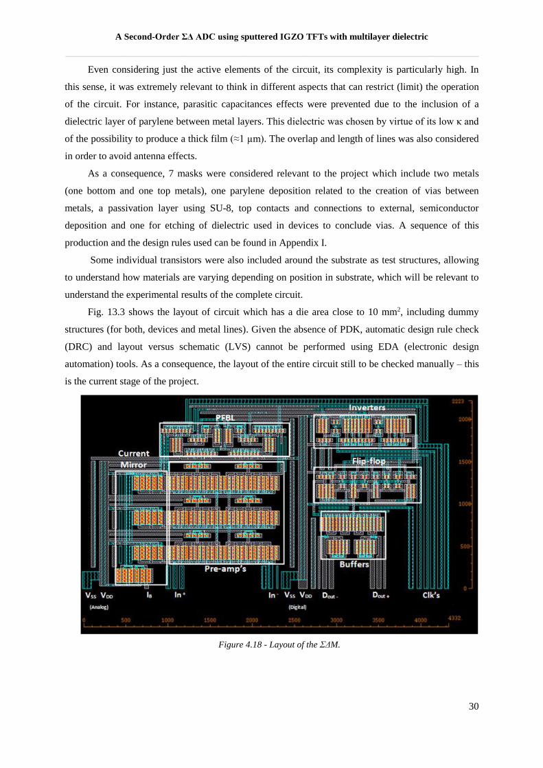
A Second-Order ΣΔ ADC using sputtered IGZO TFTs with multilayer dielectric
__________________________________________________________________________________
30
Even considering just the active elements of the circuit, its complexity is particularly high. In
this sense, it was extremely relevant to think in different aspects that can restrict (limit) the operation
of the circuit. For instance, parasitic capacitances effects were prevented due to the inclusion of a
dielectric layer of parylene between metal layers. This dielectric was chosen by virtue of its low κ and
of the possibility to produce a thick film (≈1 µm). The overlap and length of lines was also considered
in order to avoid antenna effects.
As a consequence, 7 masks were considered relevant to the project which include two metals
(one bottom and one top metals), one parylene deposition related to the creation of vias between
metals, a passivation layer using SU-8, top contacts and connections to external, semiconductor
deposition and one for etching of dielectric used in devices to conclude vias. A sequence of this
production and the design rules used can be found in Appendix I.
Some individual transistors were also included around the substrate as test structures, allowing
to understand how materials are varying depending on position in substrate, which will be relevant to
understand the experimental results of the complete circuit.
Fig. 13.3 shows the layout of circuit which has a die area close to 10 mm2, including dummy
structures (for both, devices and metal lines). Given the absence of PDK, automatic design rule check
(DRC) and layout versus schematic (LVS) cannot be performed using EDA (electronic design
automation) tools. As a consequence, the layout of the entire circuit still to be checked manually – this
is the current stage of the project.
Figure 4.18 - Layout of the ΣΔM.
A Second-Order ΣΔ ADC using sputtered IGZO TFTs with multilayer dielectric
__________________________________________________________________________________
31
5. Conclusions and Future Perspectives
This dissertation work was focused in three main topics: study and optimization of
multicomponent and multilayers dielectrics and their integration in IGZO TFTs; ΣΔM designing and
simulation using a model specially adapted for IGZO TFTs; layout of circuit for future production. In
this section, the most relevant conclusions and future perspectives about these areas will be addressed.
5.1 Conclusions
The main goal of this work was related to the usage of the IGZO TFTs with multilayer dielectric
in a 2nd-order ΣΔ ADC, which was successfully achieved, from material optimization to circuit layout.
Regarding study and optimization of dielectric layer, it was verified that multicomponent and
multilayer structure provides better dielectric properties, having a direct impact in IGZO TFT
performance:
In terms of single layer dielectrics, the co-sputtered TSiO presents a high-κ and reasonable Eg ,
despite its EB being too low for fabricating reliable devices. This mostly arises from the low band
offset between conduction bands of IGZO and Ta2O5. The TFTs produced using this dielectric present
a considerable improvement, mainly in terms of S and IG, when compared to the devices employing a
Ta2O5 layer. However, stress measurements revealed a quite significant negative ∆Von shift after 3h
stress (≈-20 V, compared to ≈-40 V of Ta2O5), suggesting a large ionic movement inside the dielectric
layer. Nonetheless, this co-sputtered layer revealed a smooth surface and an amorphous structure,
which are crucial properties for integration into multilayer configuration.
Concerning the multilayer structures, both configurations (3 and 7 layers) presented good
properties, with the structure using 7 layers providing a very large EB (>7.5 MV/cm), while
maintaining a reasonable κ (>10). When integrated in TFTs, they exhibit very low operating voltage,
low IG (<10 pA) and the magnitude of stress mechanisms is considerably reduced when compared to
TFTs with single layer dielectrics (∆Von≈1 V). As consequence, the performance of TFTs using this
layer was considered appropriate for future usage in complex circuits (after annealing at 200 ⁰C:
µSAT≈13 cm2/Vs, On/Off≈107 and S≈0.2 V/dec).
About IGZO TFT modeling, the a-Si TFT model developed by Semiconductor Devices Research
Group at RPI was adjusted and the I-V characteristics were superimposed with good accuracy. The
model only focused static characteristics but transients should also be included in future versions. Still,
the degree of accuracy of the present model was perfectly suitable to enable circuit design/simulation.
Concerning the design and the electrical simulations of the complete ΣΔM ADC, quite attractive
and encouraging results have been obtained.
The comparator circuit works at several tens of kHz with an accuracy of 10 mV. This circuit
presents a current consumption as small as 380 µA drawn from a 10 V positive power supply.
A Second-Order ΣΔ ADC using sputtered IGZO TFTs with multilayer dielectric
__________________________________________________________________________________
32
Furthermore, in order to guarantee the robustness of comparator against Von, it was also simulated
using different Von between -1 and 1 V.
Due to IGZO TFTs performance, the ΣΔM comprises a large quantity of devices. However,
simulation results show a peak SNDR of 57 dB and a DR of 65 dB (BW=500 Hz) with a power
dissipation of about 22 mW. These are considered very interesting results, going beyond the state-of-
the-art when comparing with other ADC circuit implementations based on other transistor’s
technologies, either using organic devices or even LTPS.
In terms of circuit layout, due to the fact that there was not a PDK available and it is the first
time that such a complex circuit is produced in CENIMAT, lots of details have been considered and
studied. A die area close to 10 mm2 was estimated, but this layout is, in this moment, under manually
verification.
Taking into account all work involved, the fabrication of ΣΔM will be the next stage. In fact, and
considering that there is no reference about an ADC produced using oxide TFTs, the dedication
increases and certainly a successful “prototype” will be produced in the next months – a glad
consequence of an advanced research in micro and nanoelectronics developed by CENIMAT and
CTS/UNINOVA groups.
5.2 Future Perspectives
Despite all work involved and the future production in clean room environment of the ΣΔM
ADC – which is the main future perspective - some questions and ideas remain unanswered:
Regarding TFTs, a continuous optimization is crucial to increase the complexity and
performance of circuits where they are integrated. In this sense, the influence of Ta2O5/SiO2 ratio
during dielectric deposition should be analyzed. Furthermore, the performance variation of TFTs
depending on their placement in substrate should be studied in order to understand whether there is a
gradient associated or even if deposition conditions can be improved. The significant variations
verified during stress measurements need a particular attention and investigation in order to
understand exactly the mechanisms involved and how they can be suppressed to not limit the TFT
devices’ performance.
In terms of modeling, new approaches are now being studied by group, expanding the current
static model to also consider transients, improving the accuracy of the simulation results.
After a successful fabrication of the ΣΔM ADC, a complete “integrated” ΣΔM ADC will be
investigated, being necessary to fabricate resistors and capacitors with acceptable passive device’s
mismatch – the conditions of fabrication should also be improved.
Taking into account all process, a ΣΔM using a flexible and/ or paper substrate is also a goal
for future, reinforcing the concept of flexible and recyclable electronics. The feasibility of other ADC
architectures (e.g. Nyquit rate ADCs) should also be further investigated.
A Second-Order ΣΔ ADC using sputtered IGZO TFTs with multilayer dielectric
__________________________________________________________________________________
33
6. References
[1] (23rd April 2014). Available: http://software2tech.com/
[2] (24th April 2014). Available: http://www.samsungdisplay.com/eng/index/index.jsp
[3] (25th April 2014). Available: http://www.techspot.com/news/32780-hp-unveils-flexible-
display-prototype.html
[4] A. C. Tickle, Thin-film transistors: a new approach to microelectronics: Wiley, 1969.
[5] P. Barquinha, "Transparent oxide thin-film transistors: production, characterization and
integration," Faculdade de Ciências e Tecnologia, 2010.
[6] A. Facchetti and T. J. Marks, Transparent electronics: Wiley Online Library, 2010.
[7] M. Grundmann, H. Frenzel, A. Lajn, M. Lorenz, F. Schein, and H. von Wenckstern,
"Transparent semiconducting oxides: materials and devices," physica status solidi (a), vol.
207, pp. 1437-1449, 2010.
[8] H. Q. Chiang, Development of oxide semiconductors: Materials, devices, and integration:
ProQuest, 2007.
[9] P. Barquinha, R. Martins, L. Pereira, and E. Fortunato, Transparent Oxide Electronics: From
Materials to Devices: Wiley. com, 2012.
[10] R. Hoffman, B. J. Norris, and J. Wager, "ZnO-based transparent thin-film transistors," Applied
Physics Letters, vol. 82, pp. 733-735, 2003.
[11] S. Masuda, K. Kitamura, Y. Okumura, S. Miyatake, H. Tabata, and T. Kawai, "Transparent
thin film transistors using ZnO as an active channel layer and their electrical properties,"
Journal of Applied Physics, vol. 93, pp. 1624-1630, 2003.
[12] R. L. Hoffman, "ZnO-channel thin-film transistors: Channel mobility," Journal of Applied
Physics, vol. 95, pp. 5813-5819, May 15 2004.
[13] P. Carcia, R. McLean, M. Reilly, and G. Nunes, "Transparent ZnO thin-film transistor
fabricated by rf magnetron sputtering," Applied Physics Letters, vol. 82, pp. 1117-1119, 2003.
[14] E. Fortunato, P. Barquinha, A. C. Pimentel, A. M. Gonçalves, A. J. Marques, R. F. Martins,
and L. Pereira, "Wide-bandgap high-mobility ZnO thin-film transistors produced at room
temperature," Applied Physics Letters, vol. 85, pp. 2541-2543, 2004.
[15] K. Nomura, H. Ohta, A. Takagi, T. Kamiya, M. Hirano, and H. Hosono, "Room-temperature
fabrication of transparent flexible thin-film transistors using amorphous oxide
semiconductors," Nature, vol. 432, pp. 488-492, 2004.
[16] T. Kamiya, K. Nomura, and H. Hosono, "Present status of amorphous In-Ga-Zn-O thin-film
transistors," Science and Technology of Advanced Materials, vol. 11, Aug 2010.
[17] H. Chiang, J. Wager, R. Hoffman, J. Jeong, and D. A. Keszler, "High mobility transparent
thin-film transistors with amorphous zinc tin oxide channel layer," Applied Physics Letters,
vol. 86, pp. 013503-013503-3, 2005.
[18] N. Dehuff, E. Kettenring, D. Hong, H. Chiang, J. Wager, R. Hoffman, C.-H. Park, and D.
Keszler, "Transparent thin-film transistors with zinc indium oxide channel layer," Journal of
Applied Physics, vol. 97, pp. 064505-064505-5, 2005.
[19] P. Barquinha, A. Pimentel, A. Marques, L. Pereira, R. Martins, and E. Fortunato, "Influence of
the semiconductor thickness on the electrical properties of transparent TFTs based on indium
zinc oxide," Journal of non-crystalline solids, vol. 352, pp. 1749-1752, 2006.
[20] H. Hosono, K. Nomura, Y. Ogo, T. Uruga, and T. Kamiya, "Factors controlling electron
transport properties in transparent amorphous oxide semiconductors," Journal of non-
crystalline solids, vol. 354, pp. 2796-2800, 2008.
[21] D. Kang, I. Song, C. Kim, Y. Park, T. D. Kang, H. S. Lee, J.-W. Park, S. H. Baek, S.-H. Choi,
and H. Lee, "Effect of Ga∕ In ratio on the optical and electrical properties of GaInZnO thin
films grown on SiO∕ Si substrates," Applied Physics Letters, vol. 91, p. 091910, 2007.
[22] P. Barquinha, L. Pereira, G. Goncalves, R. Martins, and E. Fortunato, "Toward high-
performance amorphous GIZO TFTs," Journal of the Electrochemical Society, vol. 156, pp.
H161-H168, 2009.
A Second-Order ΣΔ ADC using sputtered IGZO TFTs with multilayer dielectric
__________________________________________________________________________________
34
[23] E. Elangovan, K. J. Saji, S. Parthiban, G. Goncalves, P. Barquinha, R. Martins, and E.
Fortunato, "Thin-Film Transistors Based on Indium Molybdenum Oxide Semiconductor
Layers Sputtered at Room Temperature," Electron Device Letters, IEEE, vol. 32, pp. 1391-
1393, 2011.
[24] R. Martins, V. Figueiredo, R. Barros, P. Barquinha, G. Gonçalves, L. Pereira, I. Ferreira, and
E. Fortunato, "P-type oxide-based thin film transistors produced at low temperatures," 2012,
pp. 826315-826315-15.
[25] B. Meyer, A. Polity, D. Reppin, M. Becker, P. Hering, P. Klar, T. Sander, C. Reindl, J. Benz,
and M. Eickhoff, "Binary copper oxide semiconductors: From materials towards devices,"
physica status solidi (b), vol. 249, pp. 1487-1509, 2012.
[26] R. Martins, A. Nathan, R. Barros, L. Pereira, P. Barquinha, N. Correia, R. Costa, A. Ahnood,
I. Ferreira, and E. Fortunato, "Complementary Metal Oxide Semiconductor Technology With
and On Paper," Advanced Materials, vol. 23, pp. 4491-+, Oct 18 2011.
[27] J. Robertson, "Interfaces and defects of high-K oxides on silicon," Solid-State Electronics, vol.
49, pp. 283-293, 2005.
[28] J. Robertson and B. Falabretti, "Band offsets of high K gate oxides on high mobility
semiconductors," Materials Science and Engineering: B, vol. 135, pp. 267-271, 2006.
[29] J. F. Wager, "Transparent Electronics," Science, vol. 300, pp. 1245-1246, May 23, 2003 2003.
[30] L. Zhang, J. Li, X. W. Zhang, X. Y. Jiang, and Z. L. Zhang, "High-performance ZnO thin film
transistors with sputtering SiO2/Ta2O5/SiO2 multilayer gate dielectric," Thin Solid Films, vol.
518, pp. 6130-6133, Aug 2010.
[31] L. Zhang, H. Zhang, J. W. Ma, X. W. Zhang, X. Y. Jiang, and Z. L. Zhang, "Copper
phthalocyanine thin-film field-effect transistor with SiO2/Ta2O5/SiO2 multilayer insulator,"
Thin Solid Films, vol. 518, pp. 6134-6136, Aug 2010.
[32] R. S. Chen, W. Zhou, M. Zhang, M. Wong, and H. S. Kwok, "Self-aligned top-gate InGaZnO
thin film transistors using SiO2/Al2O3 stack gate dielectric," Thin Solid Films, vol. 548, pp.
572-575, Dec 2013.
[33] L. Pereira, P. Barquinha, G. Goncalves, E. Fortunato, and R. Martins, "Multicomponent
dielectrics for oxide TFT," Oxide-Based Materials and Devices Iii, vol. 8263, 2012.
[34] Y. Wang, S. W. Liu, X. W. Sun, J. L. Zhao, G. K. L. Goh, Q. V. Vu, and H. Y. Yu, "Highly
transparent solution processed In-Ga-Zn oxide thin films and thin film transistors," Journal of
Sol-Gel Science and Technology, vol. 55, pp. 322-327, Sep 2010.
[35] M. K. Ryu, K. Park, J. B. Seon, J. Park, I. Kee, Y. Lee, and S. Y. Lee, AMOLED Driven by
Solution-Processed Oxide Semiconductor TFT. Campbell: Soc Information Display, 2009.
[36] K. Song, D. Kim, X. S. Li, T. Jun, Y. Jeong, and J. Moon, "Solution processed invisible all-
oxide thin film transistors," Journal of Materials Chemistry, vol. 19, pp. 8881-8886, 2009.
[37] Y. H. Yang, S. S. Yang, C. Y. Kao, and K. S. Chou, "Chemical and Electrical Properties of
Low-Temperature Solution-Processed InGaZn-O Thin-Film Transistors," Ieee Electron
Device Letters, vol. 31, pp. 329-331, Apr 2010.
[38] K. K. Banger, Y. Yamashita, K. Mori, R. L. Peterson, T. Leedham, J. Rickard, and H.
Sirringhaus, "Low-temperature, high-performance solution-processed metal oxide thin-film
transistors formed by a 'sol-gel on chip' process," Nature Materials, vol. 10, pp. 45-50, Jan
2011.
[39] M.-G. Kim, M. G. Kanatzidis, A. Facchetti, and T. J. Marks, "Low-temperature fabrication of
high-performance metal oxide thin-film electronics via combustion processing," Nature
Materials, vol. 10, pp. 382-388, May 2011.
[40] R. F. Martins, A. Ahnood, N. Correia, L. M. Pereira, R. Barros, P. M. Barquinha, R. Costa, I.
M. Ferreira, A. Nathan, and E. E. Fortunato, "Recyclable, Flexible, Low‐Power Oxide
Electronics," Advanced Functional Materials, 2012.
[41] T. C. Carusone, D. A. Johns, and K. W. Martin, Analog Integrated Circuit Design: Wiley,
2011.
[42] B. Le, T. W. Rondeau, J. H. Reed, and C. W. Bostian, "Analog-to-digital converters," Ieee
Signal Processing Magazine, vol. 22, pp. 69-77, Nov 2005.
A Second-Order ΣΔ ADC using sputtered IGZO TFTs with multilayer dielectric
__________________________________________________________________________________
35
[43] J. L. A. de Melo, "A low power 1-MHz continuous-time ΣΔM Using a passive loop filter
designed with a genetic algorithm tool," in Circuits and Systems (ISCAS), 2013 IEEE
International Symposium on, 2013, pp. 586-589.
[44] E. Janssen and A. v. Roermund, Look-Ahead Based Sigma-Delta Modulation: Springer
Publishing Company, Incorporated, 2013.
[45] H. Marien, M. Steyaert, and P. Heremans, Analog Organic Electronics: Building Blocks for
Organic Smart Sensor Systems on Foil: Springer, 2012.
[46] R. H. Walden, "Analog-to-digital converter survey and analysis," Ieee Journal on Selected
Areas in Communications, vol. 17, pp. 539-550, Apr 1999.
[47] R. Presley, D. Hong, H. Chiang, C. Hung, R. Hoffman, and J. Wager, "Transparent ring
oscillator based on indium gallium oxide thin-film transistors," Solid-State Electronics, vol.
50, pp. 500-503, 2006.
[48] M. Mativenga, M. H. Choi, J. W. Choi, and J. Jang, "Transparent Flexible Circuits Based on
Amorphous-Indium-Gallium-Zinc-Oxide Thin-Film Transistors," Ieee Electron Device
Letters, vol. 32, pp. 170-172, Feb 2011.
[49] B. Kim, C. I. Ryoo, S. J. Kim, J. U. Bae, H. S. Seo, C. D. Kim, and M. K. Han, "New
Depletion-Mode IGZO TFT Shift Register," Ieee Electron Device Letters, vol. 32, pp. 158-
160, Feb 2011.
[50] D. Raiteri, F. Torricelli, K. Myny, M. Nag, B. van der Putten, E. Smits, S. Steudel, K.
Tempelaars, A. Tripathi, G. Gelinck, A. van Roermund, and E. Cantatore, "A 6b 10MS/s
current-steering DAC manufactured with amorphous Gallium-Indium-Zinc-Oxide TFTs
achieving SFDR ˃ 30dB up to 300kHz," in Solid-State Circuits Conference Digest of
Technical Papers (ISSCC), 2012 IEEE International, 2012, pp. 314-316.
[51] A. Dey, D. R. Allee, and Ieee, Amorphous Silicon 5 Bit Flash Analog to Digital Converter,
2012.
[52] A. Jamshidi-Roudbari, P.-C. Kuo, and M. K. Hatalis, "A flash analog to digital converter on
stainless steel foil substrate," Solid-State Electronics, vol. 54, pp. 410-416, Apr 2010.
[53] W.-M. Lin, C.-F. Lin, S.-I. Liu, and Ieee, A CBSC Second-Order Sigma-Delta Modulator in 3
mu m LTPS-TFT Technology, 2009.
[54] X. Wei, U. Zschieschang, H. Klauk, and B. Murmann, "A 3V 6b successive-approximation
ADC using complementary organic thin-film transistors on glass," in Solid-State Circuits
Conference Digest of Technical Papers (ISSCC), 2010 IEEE International, 2010, pp. 134-135.
[55] H. Marien, M. S. J. Steyaert, E. van Veenendaal, and P. Heremans, "A Fully Integrated Delta
Sigma ADC in Organic Thin-Film Transistor Technology on Flexible Plastic Foil," Ieee
Journal of Solid-State Circuits, vol. 46, pp. 276-284, Jan 2011.
[56] C. Chaneliere, S. Four, J. Autran, and R. Devine, "Comparison between the properties of
amorphous and crystalline Ta2O5 thin films deposited on Si," Microelectronics Reliability,
vol. 39, pp. 261-268, 1999.
[57] D. K. Schroder, Semiconductor material and device characterization: John Wiley & Sons,
2006.
[58] J. F. Conley, "Instabilities in Amorphous Oxide Semiconductor Thin-Film Transistors,"
Device and Materials Reliability, IEEE Transactions on, vol. 10, pp. 460-475, 2010.
[59] D. Kang, H. Lim, C. Kim, I. Song, J. Park, Y. Park, and J. Chung, "Amorphous gallium
indium zinc oxide thin film transistors: Sensitive to oxygen molecules," Applied physics
letters, vol. 90, p. 192101, 2007.
[60] J. L. A. de Melo, F. Querido, N. Paulino, and J. Goes, "A 0.4-V 410-nW opamp-less
continuous-time ΣΔ modulator for biomedical applications," in Circuits and Systems (ISCAS),
2014 IEEE International Symposium on, 2014, pp. 1340-1343.
[61] J. L. A. De Melo, B. Nowacki, N. Paulino, and J. Goes, "Design methodology for Sigma-Delta
modulators based on a genetic algorithm using hybrid cost functions," in Circuits and Systems
(ISCAS), 2012 IEEE International Symposium on, 2012, pp. 301-304.
[62] N. P. Barradas, C. Jeynes, and R. P. Webb, "Simulated annealing analysis of Rutherford
backscattering data," Applied Physics Letters, vol. 71, pp. 291-293, 1997.
A Second-Order ΣΔ ADC using sputtered IGZO TFTs with multilayer dielectric
__________________________________________________________________________________
36
[63] P. Barquinha, A. M. Vilà, G. Gonçalves, L. Pereira, R. Martins, J. R. Morante, and E.
Fortunato, "Gallium–indium–zinc-oxide-based thin-film transistors: influence of the
source/drain material," Electron Devices, IEEE Transactions on, vol. 55, pp. 954-960, 2008.
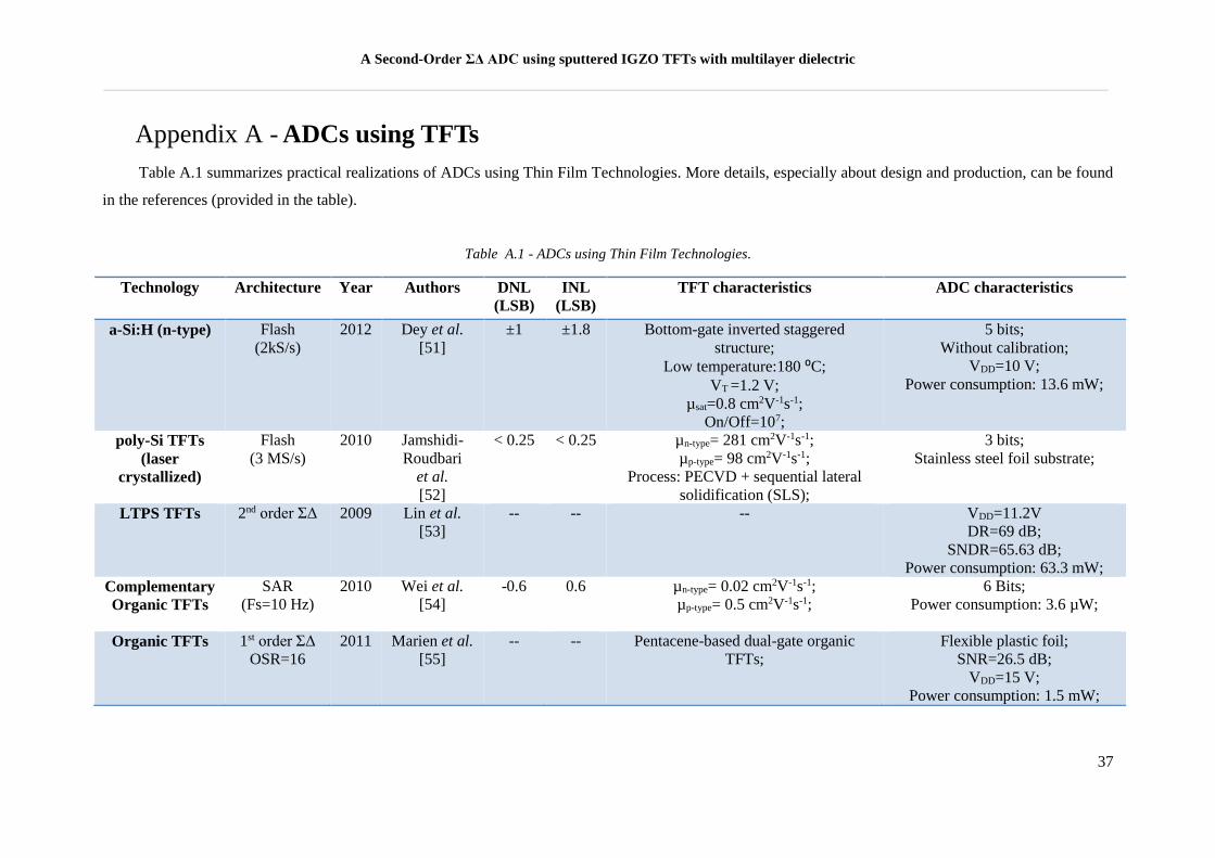
A Second-Order ΣΔ ADC using sputtered IGZO TFTs with multilayer dielectric
______________________________________________________________________________________________________________________________
37
Appendix A - ADCs using TFTs
Table A.1 summarizes practical realizations of ADCs using Thin Film Technologies. More details, especially about design and production, can be found
in the references (provided in the table).
Table A.1 - ADCs using Thin Film Technologies.
Technology Architecture Year Authors DNL
(LSB)
INL
(LSB)
TFT characteristics ADC characteristics
a-Si:H (n-type) Flash
(2kS/s)
2012 Dey et al.
[51]
±1 ±1.8 Bottom-gate inverted staggered
structure;
Low temperature:180 ⁰C;
VT =1.2 V;
µsat=0.8 cm2V-1s-1;
On/Off=107;
5 bits;
Without calibration;
VDD=10 V;
Power consumption: 13.6 mW;
poly-Si TFTs
(laser
crystallized)
Flash
(3 MS/s)
2010 Jamshidi-
Roudbari
et al.
[52]
< 0.25 < 0.25 µn-type= 281 cm2V-1s-1;
µp-type= 98 cm2V-1s-1;
Process: PECVD + sequential lateral
solidification (SLS);
3 bits;
Stainless steel foil substrate;
LTPS TFTs 2nd order ΣΔ
2009 Lin et al.
[53]
-- -- -- VDD=11.2V
DR=69 dB;
SNDR=65.63 dB;
Power consumption: 63.3 mW;
Complementary
Organic TFTs
SAR
(Fs=10 Hz)
2010 Wei et al.
[54]
-0.6 0.6 µn-type= 0.02 cm2V-1s-1;
µp-type= 0.5 cm2V-1s-1;
6 Bits;
Power consumption: 3.6 µW;
Organic TFTs 1st order ΣΔ
OSR=16
2011 Marien et al.
[55]
-- -- Pentacene-based dual-gate organic
TFTs;
Flexible plastic foil;
SNR=26.5 dB;
VDD=15 V;
Power consumption: 1.5 mW;

A Second-Order ΣΔ ADC using sputtered IGZO TFTs with multilayer dielectric
__________________________________________________________________________________
38
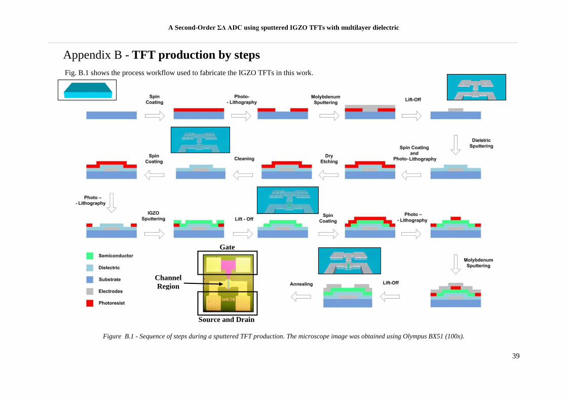
A Second-Order ΣΔ ADC using sputtered IGZO TFTs with multilayer dielectric
______________________________________________________________________________________________________________________________
39
Appendix B - TFT production by steps
Fig. B.1 shows the process workflow used to fabricate the IGZO TFTs in this work.
Figure B.1 - Sequence of steps during a sputtered TFT production. The microscope image was obtained using Olympus BX51 (100x).
Gate
Source and Drain
Channel
Region

A Second-Order ΣΔ ADC using sputtered IGZO TFTs with multilayer dielectric
__________________________________________________________________________________
40
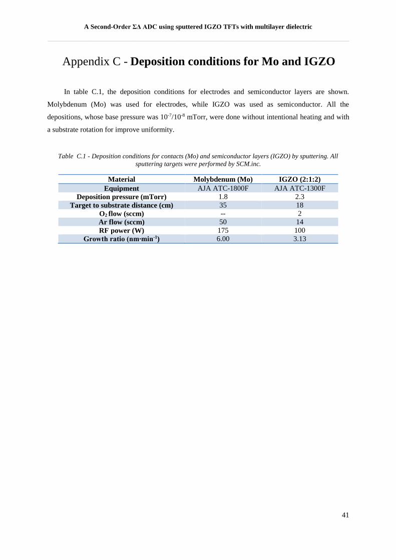
A Second-Order ΣΔ ADC using sputtered IGZO TFTs with multilayer dielectric
__________________________________________________________________________________
41
Appendix C - Deposition conditions for Mo and IGZO
In table C.1, the deposition conditions for electrodes and semiconductor layers are shown.
Molybdenum (Mo) was used for electrodes, while IGZO was used as semiconductor. All the
depositions, whose base pressure was 10-7/10-8 mTorr, were done without intentional heating and with
a substrate rotation for improve uniformity.
Table C.1 - Deposition conditions for contacts (Mo) and semiconductor layers (IGZO) by sputtering. All
sputtering targets were performed by SCM.inc.
Material Molybdenum (Mo) IGZO (2:1:2)
Equipment AJA ATC-1800F AJA ATC-1300F
Deposition pressure (mTorr) 1.8 2.3
Target to substrate distance (cm) 35 18
O2 flow (sccm) -- 2
Ar flow (sccm) 50 14
RF power (W) 175 100
Growth ratio (nm∙min-1) 6.00 3.13

A Second-Order ΣΔ ADC using sputtered IGZO TFTs with multilayer dielectric
__________________________________________________________________________________
42
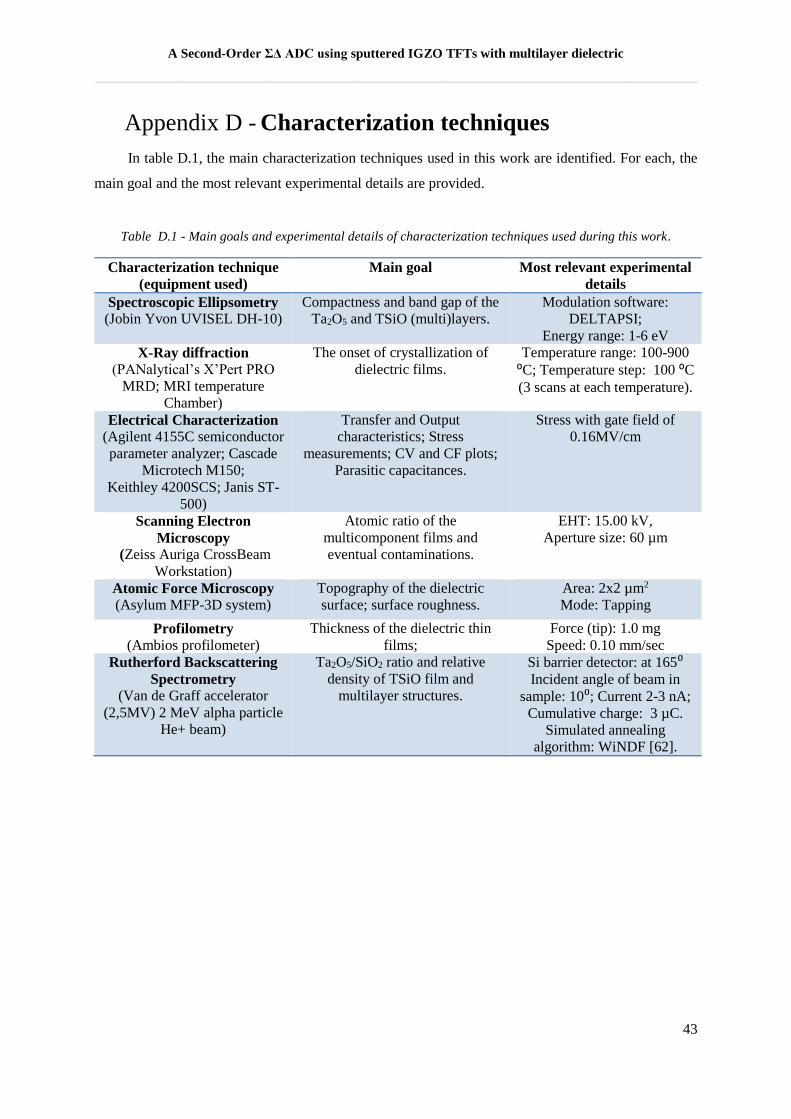
A Second-Order ΣΔ ADC using sputtered IGZO TFTs with multilayer dielectric
__________________________________________________________________________________
43
Appendix D - Characterization techniques
In table D.1, the main characterization techniques used in this work are identified. For each, the
main goal and the most relevant experimental details are provided.
Table D.1 - Main goals and experimental details of characterization techniques used during this work.
Characterization technique
(equipment used)
Main goal Most relevant experimental
details
Spectroscopic Ellipsometry
(Jobin Yvon UVISEL DH-10)
Compactness and band gap of the
Ta2O5 and TSiO (multi)layers.
Modulation software:
DELTAPSI;
Energy range: 1-6 eV
X-Ray diffraction
(PANalytical’s X’Pert PRO
MRD; MRI temperature
Chamber)
The onset of crystallization of
dielectric films.
Temperature range: 100-900
⁰C; Temperature step: 100 ⁰C
(3 scans at each temperature).
Electrical Characterization
(Agilent 4155C semiconductor
parameter analyzer; Cascade
Microtech M150;
Keithley 4200SCS; Janis ST-
500)
Transfer and Output
characteristics; Stress
measurements; CV and CF plots;
Parasitic capacitances.
Stress with gate field of
0.16MV/cm
Scanning Electron
Microscopy
(Zeiss Auriga CrossBeam
Workstation)
Atomic ratio of the
multicomponent films and
eventual contaminations.
EHT: 15.00 kV,
Aperture size: 60 µm
Atomic Force Microscopy
(Asylum MFP-3D system)
Topography of the dielectric
surface; surface roughness.
Area: 2x2 µm2
Mode: Tapping
Profilometry
(Ambios profilometer)
Thickness of the dielectric thin
films;
Force (tip): 1.0 mg
Speed: 0.10 mm/sec
Rutherford Backscattering
Spectrometry
(Van de Graff accelerator
(2,5MV) 2 MeV alpha particle
He+ beam)
Ta2O5/SiO2 ratio and relative
density of TSiO film and
multilayer structures.
Si barrier detector: at 165⁰ Incident angle of beam in
sample: 10⁰; Current 2-3 nA;
Cumulative charge: 3 µC.
Simulated annealing
algorithm: WiNDF [62].

A Second-Order ΣΔ ADC using sputtered IGZO TFTs with multilayer dielectric
__________________________________________________________________________________
44
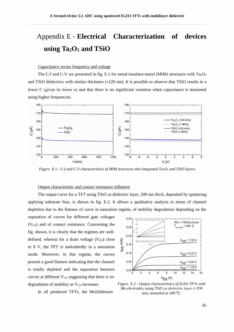
A Second-Order ΣΔ ADC using sputtered IGZO TFTs with multilayer dielectric
__________________________________________________________________________________
45
Figure E.1 - C-f and C-V characteristics of MIM structures that integrated Ta2O5 and TSiO layers.
Figure E.2 - Output characteristics of IGZO TFTs with
Mo electrodes, using TSiO as dielectric layer (≈200
nm), annealed at 200 ⁰C.
Appendix E - Electrical Characterization of devices
using Ta2O5 and TSiO
Capacitance versus frequency and voltage
The C-f and C-V are presented in fig. E.1 for metal-insulator-metal (MIM) structures with Ta2O5
and TSiO dielectrics with similar thickness (≈220 nm). It is possible to observe that TSiO results in a
lower C (given its lower κ) and that there is no significant variation when capacitance is measured
using higher frequencies.
Output characteristic and contact resistance influence
The output curve for a TFT using TSiO as dielectric layer, 200 nm thick, deposited by sputtering
applying substrate bias, is shown in fig. E.2. It allows a qualitative analysis in terms of channel
depletion due to the flatness of curve in saturation regime, of mobility degradation depending on the
separation of curves for different gate voltages
(VGS) and of contact resistance. Concerning the
fig. shown, it is clearly that the regimes are well-
defined, wherein for a drain voltage (VDS) close
to 8 V, the TFT is undoubtedly in a saturation
mode. Moreover, in this regime, the curves
present a good flatness indicating that the channel
is totally depleted and the separation between
curves at different VGS suggesting that there is no
degradation of mobility as VGS increases.
In all produced TFTs, the Molybdenum
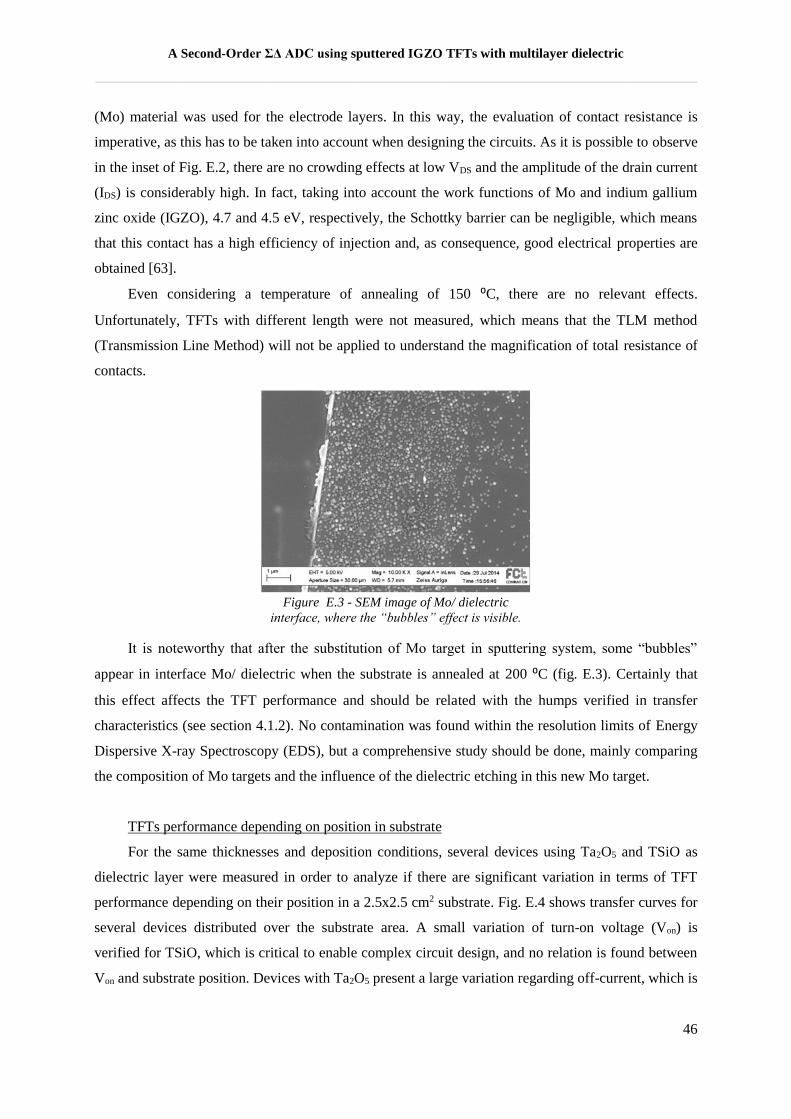
A Second-Order ΣΔ ADC using sputtered IGZO TFTs with multilayer dielectric
__________________________________________________________________________________
46
Figure E.3 - SEM image of Mo/ dielectric
interface, where the “bubbles” effect is visible.
(Mo) material was used for the electrode layers. In this way, the evaluation of contact resistance is
imperative, as this has to be taken into account when designing the circuits. As it is possible to observe
in the inset of Fig. E.2, there are no crowding effects at low VDS and the amplitude of the drain current
(IDS) is considerably high. In fact, taking into account the work functions of Mo and indium gallium
zinc oxide (IGZO), 4.7 and 4.5 eV, respectively, the Schottky barrier can be negligible, which means
that this contact has a high efficiency of injection and, as consequence, good electrical properties are
obtained [63].
Even considering a temperature of annealing of 150 ⁰C, there are no relevant effects.
Unfortunately, TFTs with different length were not measured, which means that the TLM method
(Transmission Line Method) will not be applied to understand the magnification of total resistance of
contacts.
It is noteworthy that after the substitution of Mo target in sputtering system, some “bubbles”
appear in interface Mo/ dielectric when the substrate is annealed at 200 ⁰C (fig. E.3). Certainly that
this effect affects the TFT performance and should be related with the humps verified in transfer
characteristics (see section 4.1.2). No contamination was found within the resolution limits of Energy
Dispersive X-ray Spectroscopy (EDS), but a comprehensive study should be done, mainly comparing
the composition of Mo targets and the influence of the dielectric etching in this new Mo target.
TFTs performance depending on position in substrate
For the same thicknesses and deposition conditions, several devices using Ta2O5 and TSiO as
dielectric layer were measured in order to analyze if there are significant variation in terms of TFT
performance depending on their position in a 2.5x2.5 cm2 substrate. Fig. E.4 shows transfer curves for
several devices distributed over the substrate area. A small variation of turn-on voltage (Von) is
verified for TSiO, which is critical to enable complex circuit design, and no relation is found between
Von and substrate position. Devices with Ta2O5 present a large variation regarding off-current, which is
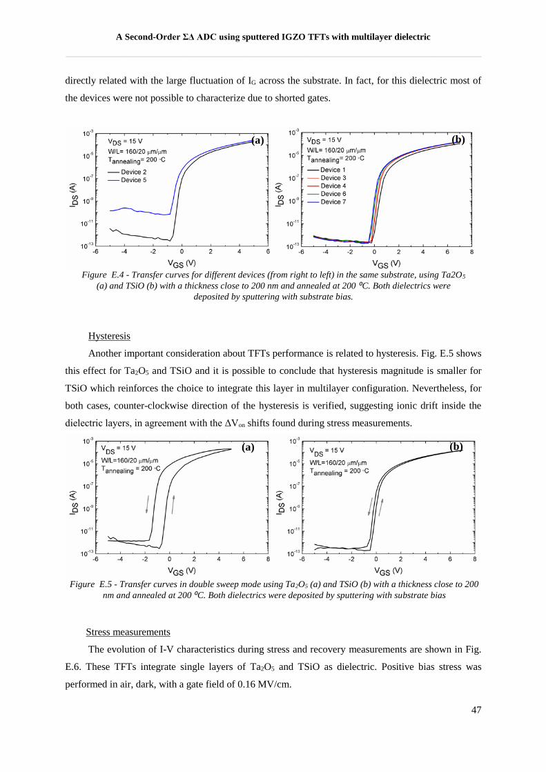
A Second-Order ΣΔ ADC using sputtered IGZO TFTs with multilayer dielectric
__________________________________________________________________________________
47
(a) (b)
Figure E.4 - Transfer curves for different devices (from right to left) in the same substrate, using Ta2O5
(a) and TSiO (b) with a thickness close to 200 nm and annealed at 200 ⁰C. Both dielectrics were
deposited by sputtering with substrate bias.
(a) (b)
Figure E.5 - Transfer curves in double sweep mode using Ta2O5 (a) and TSiO (b) with a thickness close to 200
nm and annealed at 200 ⁰C. Both dielectrics were deposited by sputtering with substrate bias
directly related with the large fluctuation of IG across the substrate. In fact, for this dielectric most of
the devices were not possible to characterize due to shorted gates.
Hysteresis
Another important consideration about TFTs performance is related to hysteresis. Fig. E.5 shows
this effect for Ta2O5 and TSiO and it is possible to conclude that hysteresis magnitude is smaller for
TSiO which reinforces the choice to integrate this layer in multilayer configuration. Nevertheless, for
both cases, counter-clockwise direction of the hysteresis is verified, suggesting ionic drift inside the
dielectric layers, in agreement with the ΔVon shifts found during stress measurements.
Stress measurements
The evolution of I-V characteristics during stress and recovery measurements are shown in Fig.
E.6. These TFTs integrate single layers of Ta2O5 and TSiO as dielectric. Positive bias stress was
performed in air, dark, with a gate field of 0.16 MV/cm.
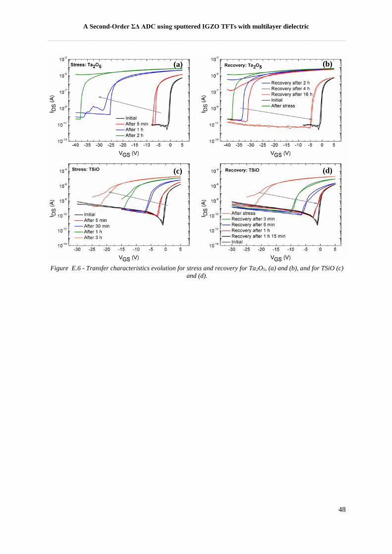
A Second-Order ΣΔ ADC using sputtered IGZO TFTs with multilayer dielectric
__________________________________________________________________________________
48
(c) (d)
(a) (b)
Figure E.6 - Transfer characteristics evolution for stress and recovery for Ta2O5, (a) and (b), and for TSiO (c)
and (d).
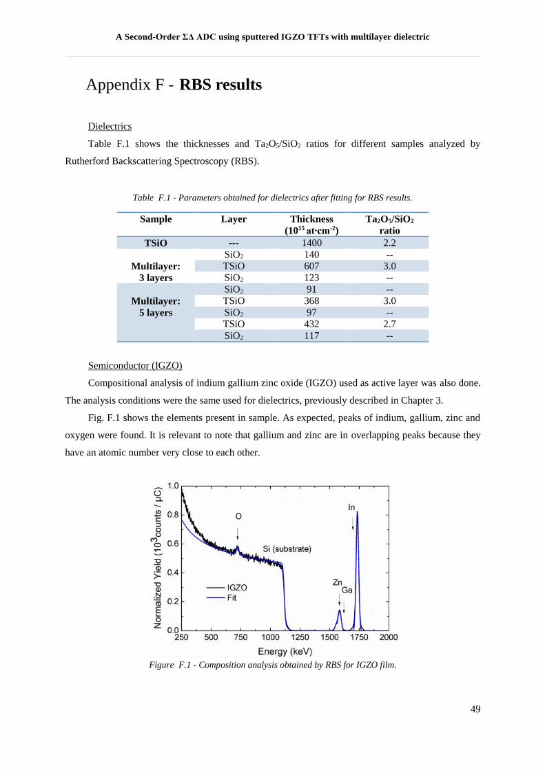
A Second-Order ΣΔ ADC using sputtered IGZO TFTs with multilayer dielectric
__________________________________________________________________________________
49
Figure F.1 - Composition analysis obtained by RBS for IGZO film.
Appendix F - RBS results
Dielectrics
Table F.1 shows the thicknesses and Ta2O5/SiO2 ratios for different samples analyzed by
Rutherford Backscattering Spectroscopy (RBS).
Table F.1 - Parameters obtained for dielectrics after fitting for RBS results.
Sample Layer Thickness
(1015 at∙cm-2)
Ta2O5/SiO2
ratio
TSiO --- 1400 2.2
Multilayer:
3 layers
SiO2 140 --
TSiO 607 3.0
SiO2 123 --
Multilayer:
5 layers
SiO2 91 --
TSiO 368 3.0
SiO2 97 --
TSiO 432 2.7
SiO2 117 --
Semiconductor (IGZO)
Compositional analysis of indium gallium zinc oxide (IGZO) used as active layer was also done.
The analysis conditions were the same used for dielectrics, previously described in Chapter 3.
Fig. F.1 shows the elements present in sample. As expected, peaks of indium, gallium, zinc and
oxygen were found. It is relevant to note that gallium and zinc are in overlapping peaks because they
have an atomic number very close to each other.
A Second-Order ΣΔ ADC using sputtered IGZO TFTs with multilayer dielectric
__________________________________________________________________________________
50
However, according to the percentages of elements determined, an atomic ratio of 4:2:1
(indium:gallium:zinc) was found which is equivalent to 2:1:1 in terms of molecular ratio
(In2O3:Ga2O3:ZnO).
Table F.2 - RBS results obtained after fitting of IGZO data.
Sample Thickness
(1015 at∙cm-2)
In
(at. %)
Ga
(at. %)
Zn
(at.%)
O
(at.%)
Ar
(at. %) 2
IGZO 202 21.7 9.6 4.5 63.6 0.5 6.42
A Second-Order ΣΔ ADC using sputtered IGZO TFTs with multilayer dielectric
__________________________________________________________________________________
51
Appendix G - Electrical Characterization of devices
using Multilayer structures
Electrical Properties – summary
Electrical properties of TFTs integrating multilayer structures were analyzed and they are
presented in table G.1. For 3 layers configuration, three different thicknesses were evaluated, ranging
from 100 to 250 nm. Taking into account that the TFT with 200 nm of dielectric layer provided the
best performance, the 7 layers structures were produced considering, approximately the same
thickness.
Table G.1 - Electrical properties for TFT devices that used multilayers structures (W/L = 160/20 µm/µm).
Devices were measured using a short integration time to prevent hump effects (see chapter 4), which increases
the measured IG values over more conventional medium integration times.
Multilayer Temperature Thickness
(nm)
µsat
(cm2∙V-1∙s-1)
On-off
ratio
Von
(V)
S
(V∙dec-
1)
IG @ VGmax
(A)
3 layers 150 250.0 14.5 4.21×10⁸ -0.75 0.176 1.51×10⁻¹⁰ 3 layers 150 200.0 14.6 8.36×10⁸ -2.00 0.177 6.80×10⁻¹³
3 layers 150 100.0 24.9 6.31×10⁵ -0.25 0.182 1.78×10⁻¹⁰
7 layers 200 240.0 12.7 3.23×10⁷ -1.50 0.213 1.26×10⁻¹⁰
Stress measurements
The evolution of transfer characteristics during stress and recovery measurements are shown in
fig. G.1. These TFTs integrate multilayer structure as dielectric. A large improvement is verified when
comparing these plots with the ones of TFTs having single layer dielectrics (fig. E.6).
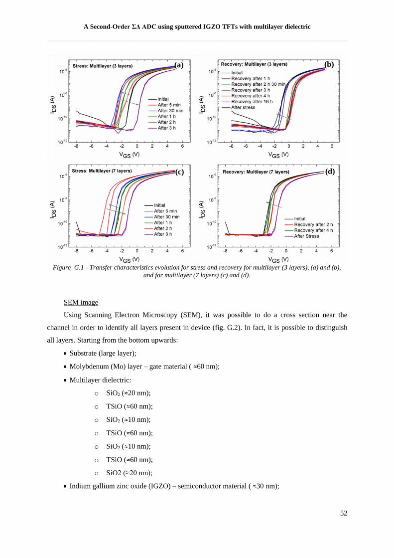
A Second-Order ΣΔ ADC using sputtered IGZO TFTs with multilayer dielectric
__________________________________________________________________________________
52
(a) (b)
(c) (d)
Figure G.1 - Transfer characteristics evolution for stress and recovery for multilayer (3 layers), (a) and (b),
and for multilayer (7 layers) (c) and (d).
SEM image
Using Scanning Electron Microscopy (SEM), it was possible to do a cross section near the
channel in order to identify all layers present in device (fig. G.2). In fact, it is possible to distinguish
all layers. Starting from the bottom upwards:
Substrate (large layer);
Molybdenum (Mo) layer – gate material ( ≈60 nm);
Multilayer dielectric:
o SiO2 (≈20 nm);
o TSiO (≈60 nm);
o SiO2 (≈10 nm);
o TSiO (≈60 nm);
o SiO2 (≈10 nm);
o TSiO (≈60 nm);
o SiO2 (≈20 nm);
Indium gallium zinc oxide (IGZO) – semiconductor material ( ≈30 nm);
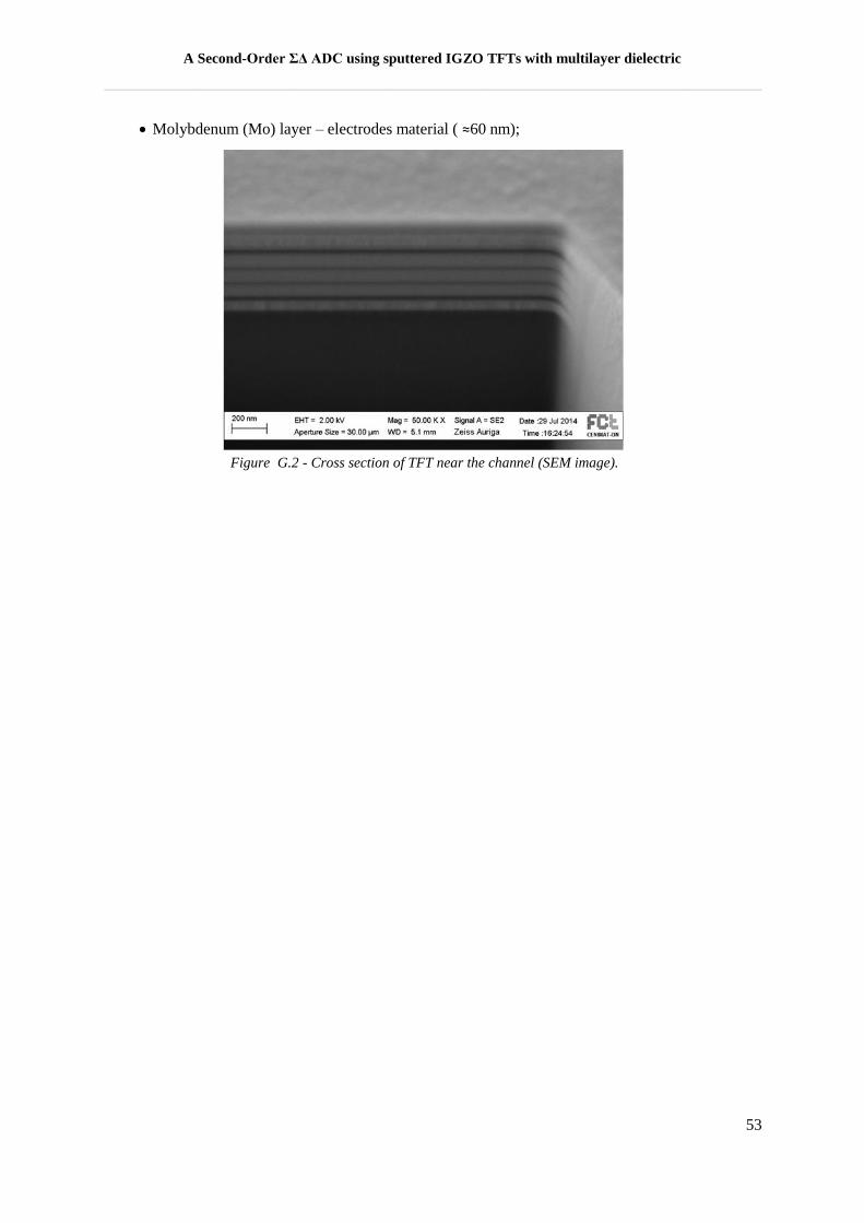
A Second-Order ΣΔ ADC using sputtered IGZO TFTs with multilayer dielectric
__________________________________________________________________________________
53
Figure G.2 - Cross section of TFT near the channel (SEM image).
Molybdenum (Mo) layer – electrodes material ( ≈60 nm);

A Second-Order ΣΔ ADC using sputtered IGZO TFTs with multilayer dielectric
__________________________________________________________________________________
54
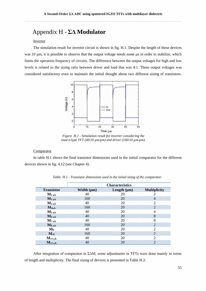
A Second-Order ΣΔ ADC using sputtered IGZO TFTs with multilayer dielectric
__________________________________________________________________________________
55
Appendix H - ΣΔ Modulator
Inverter
The simulation result for inverter circuit is shown in fig. H.1. Despite the length of these devices
was 10 µm, it is possible to observe that the output voltage needs some µs in order to stabilize, which
limits the operation frequency of circuits. The difference between the output voltages for high and low
levels is related to the sizing ratio between driver and load that was 4:1. These output voltages was
considered satisfactory even to maintain the initial thought about two different sizing of transistors.
Comparator
In table H.1 shows the final transistor dimensions used in the initial comparator for the different
devices shown in fig. 4.12 (see Chapter 4).
Table H.1 - Transistor dimensions used in the initial sizing of the comparator.
Characteristics
Transistor Width (µm) Length (µm) Multiplicity
M1 a,b 40 20 2
M2 a,b 160 20 4
M3 a,b 40 20 2
M4a,b 160 20 2
M5 a,b 40 20 4
M6 a,b 40 20 8
M7 a,b 40 20 8
M8 a,b 160 20 2
M9 40 20 2
M10 160 20 2
M11 a,b 40 20 2
M12 a,b 40 20 2
After integration of comparator in ΣΔM, some adjustments in TFTs were done mainly in terms
of length and multiplicity. The final sizing of devices is presented in Table H.2.
Figure H.1 - Simulation result for inverter considering the
load n-type TFT (40/10 µm/µm) and driver (160/10 µm/µm).
A Second-Order ΣΔ ADC using sputtered IGZO TFTs with multilayer dielectric
__________________________________________________________________________________
56
Table H.2 - Transistor dimensions used in the final sizing of the comparator.
Characteristics
Transistor Width (µm) Length (µm) Multiplicity
M1 a,b 40 40 2
M2 a,b 160 20 12
M3 a,b 40 10 2
M4a,b 160 10 2
M5 a,b 40 10 4
M6 a,b 40 10 8
M7 a,b 40 10 8
M8 a,b 160 10 2
M9 40 10 2
M10 160 10 2
M11 a,b 40 10 2
M12 a,b 40 10 2
Modulator
According to SIMULINK® results, the values of passive components illustrated in fig. 4.15b,
are presented in Table H.3.
Table H.3 - Sizing of passive elements obtained by SIMULINK®.
Component Value
R1 a,b 111.0 kΩ
R2 a,b 64.4 kΩ
R3 a,b 116.3 kΩ
R4 a,b 271.6 kΩ
R5 a,b 25.05 kΩ
C1 2.2 nF
C2 2.2 nF
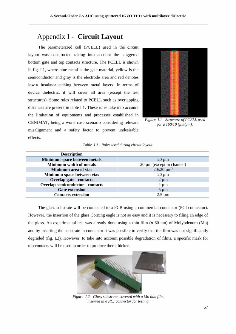
A Second-Order ΣΔ ADC using sputtered IGZO TFTs with multilayer dielectric
__________________________________________________________________________________
57
Figure I.2 - Glass substrate, covered with a Mo thin film,
inserted in a PCI connector for testing.
Appendix I - Circuit Layout
The parameterized cell (PCELL) used in the circuit
layout was constructed taking into account the staggered
bottom gate and top contacts structure. The PCELL is shown
in fig. I.1, where blue metal is the gate material, yellow is the
semiconductor and gray is the electrode area and red denotes
low-κ insulator etching between metal layers. In terms of
device dielectric, it will cover all area (except the test
structures). Some rules related to PCELL such as overlapping
distances are present in table I.1. These rules take into account
the limitation of equipments and processes established in
CENIMAT, being a worst-case scenario considering relevant
misalignment and a safety factor to prevent undesirable
effects.
Table I.1 - Rules used during circuit layout.
Description
Minimum space between metals 20 µm
Minimum width of metals 20 µm (except in channel)
Minimum area of vias 20x20 µm2
Minimum space between vias 20 µm
Overlap gate - contacts 2 µm
Overlap semiconductor - contacts 4 µm
Gate extension 5 µm
Contacts extension 2.5 µm
The glass substrate will be connected to a PCB using a commercial connector (PCI connector).
However, the insertion of the glass Corning eagle is not so easy and it is necessary to filing an edge of
the glass. An experimental test was already done using a thin film (≈ 60 nm) of Molybdenum (Mo)
and by inserting the substrate in connector it was possible to verify that the film was not significantly
degraded (fig. I.2). However, to take into account possible degradation of films, a specific mask for
top contacts will be used in order to produce them thicker.
Figure I.1 - Structure of PCELL used
for a 160/10 (µm/µm).
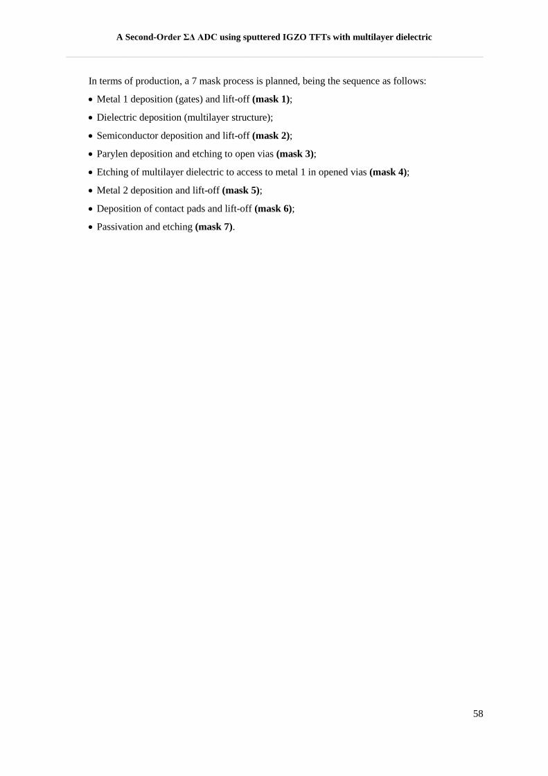
A Second-Order ΣΔ ADC using sputtered IGZO TFTs with multilayer dielectric
__________________________________________________________________________________
58
In terms of production, a 7 mask process is planned, being the sequence as follows:
Metal 1 deposition (gates) and lift-off (mask 1);
Dielectric deposition (multilayer structure);
Semiconductor deposition and lift-off (mask 2);
Parylen deposition and etching to open vias (mask 3);
Etching of multilayer dielectric to access to metal 1 in opened vias (mask 4);
Metal 2 deposition and lift-off (mask 5);
Deposition of contact pads and lift-off (mask 6);
Passivation and etching (mask 7).