Embed Size (px)
Citation preview
A Ripple-based Ultra-low Power Buck Converter with Constant On-Time
Control
BY
Saikiran Reddy Ramidi, B.E
A technical report submitted to the Graduate School in partial
fulfillment of the requirements
for the degree
Master of Sciences, Engineering
Specialization in: Electrical Engineering
New Mexico State University
Las Cruces, New Mexico
July 2017
“A Ripple-based Ultra-Low Power Buck Converter with Constant On-Time Con-
trol,” a technical report prepared by Saikiran Reddy Ramidi in partial fulfillment
of the requirements for the degree, Master of Sciences has been approved and
accepted by the following:
Dr. Louis ReyesDean of the Graduate School
Chair of the Examining Committee
Date
Committee in charge:
Dr. Paul M. Furth, Associate Professor, Chair.
Dr. Wei Tang, Assistant Professor.
Dr. Rolfe Sassenfeld, Associate Professor.
ii

DEDICATION
Dedicated to my father Bhoopal Reddy Ramidi, mother Lakshmi Ramidi,
sister Neha Ramidi, my advisor Dr. Paul Furth and my family members.
iii

ACKNOWLEDGMENTS
I thank my parents Bhoopal Reddy Ramidi and Lakshmi Ramidi for encour-
aging me to pursue Masters program. Your strong support and encouragement
kept me focused on my academics.
It is a great privilege to have Dr. Paul Furth as my advisor. He is not only
a great teacher but also a wonderful human being. His way of teaching not only
helped me gain great intuition of several concepts, but more importantly taught
me a new way of approaching a problem and new ways of learning.
Thank you my friends and roommates Saikrishna Nelluri, Suresh Badavath,
Karthik Panuganti, Mahender Manda and Harsha Gadde for making las cruces
feel like home. It was great joy being with you all.
Mahender Manda was a great company. The discussions we had on several
topics and the questions you ask pushed me to have more intuition on any topic.
I am also privileged to have Sri Harsh Pakala as my mentor and an advisor.
I thank him for having patience in answering even the silliest questions and for
guiding me both academically and personally.
I would like to specially thank my VLSI team friends Ravindra Jonnala-
gadda, Venu Siripurapu, Rohith Gaddam, Pradeep kumar Polavarapu, Kumar Pal
iv

Mandoth and Arun Kumar Bijjala. You made the work environment (classes and
lab) more fun.
I would like to thank Vamshidhar Reddy Rajannagari for his guidance and
support.
Being with Yeshwanth Puppala was great fun. I would like to thank him
for his guidance and support.
I would like to thank Harish Nammi for being my mentor. It is great
working with you and talking to you.
I would like to thank all other friends in las cruces who filled this place with
fun and joy, Saikiran Golconda, Akhilesh Kumar, Om Rameshwar Gatla, Ankith
Nadella, Hemanth Pendyala, Niranjan Eshappa, Chaitanya Kukutla, Sachin Sunka,
Narapa Bommu, Bala Kesavaraju Nadikatla, Bhanu Pinnapu, Yashwanth Madadi,
Nagendra Kalava Phanidhar Kukutla, Harvind Kumar, Gangadhar Pulipelli, Phani
Raj Dandamudi, Sujith Dandamudi, Avinash Savvy, Jyoteesh, Sreyas Kundurpi,
Charan Yellanki, Hemanth Bondilli, Manikanta Ponnam, Dinesh, Srinath Pin-
napu, Pranay Kumar Lingala, Bhumika Parikh, Tapaswy Muppaneni and Pavan
Chaturvedi.
v
ABSTRACT
A Ripple-based Ultra-low Power Buck Converter with Constant On-Time
Control
BY
Saikiran Reddy Ramidi, B.E
Master of Sciences, Engineering
Specialization in Electrical Engineering
New Mexico State University
Las Cruces, New Mexico, 2017
Dr. Paul M. Furth, Chair
MS Technical Report defense scheduled on 07/07/2017, 9 AM
Thomas & Brown Hall, Room 207.
Ultra-low power applications such as fitness tracking devices, which are
always carried by the users, so that the body activity is monitored round the clock,
requires the battery to run continually. As such, there is a demand for long battery
run-time (time to drain a fully charged battery before needing to recharge it) for
these devices. However, the battery size is limited which also limits the amount of
battery energy available. Therefore, a highly efficient DC-DC converter is needed
to improve the battery run-time. A highly efficient DC-DC buck converter for
vi

ultra-low power applications is proposed in this work. A ripple-based ultra-low
power buck converter with constant on-time control is implemented in IBM 180
nm CMOS technology. The implemented DC-DC buck converter can drive loads
from 20 µA to 200 µA. Power losses in the buck converter are understood before
implementing the design. A simulated peak efficiency of 87.1% is achieved with
the implemented design.
vii
TABLE OF CONTENTS
LIST OF TABLES xi
LIST OF FIGURES xii
1 INTRODUCTION 1
1.1 Motivation . . . . . . . . . . . . . . . . . . . . . . . . . . . . . . . 1
1.2 Objectives and Unique Contributions . . . . . . . . . . . . . . . . 2
1.3 Report Organization . . . . . . . . . . . . . . . . . . . . . . . . . 3
2 LITERATURE REVIEW 4
2.1 DC-DC Buck Converter . . . . . . . . . . . . . . . . . . . . . . . 4
2.1.1 Conventional DC-DC Buck Converter . . . . . . . . . . . . 4
2.1.2 Synchronous DC-DC Buck Converter . . . . . . . . . . . . 8
2.2 Modes of Operation . . . . . . . . . . . . . . . . . . . . . . . . . . 11
2.3 Control Techniques in a Buck Converter . . . . . . . . . . . . . . 13
2.3.1 Pulse Width Modulation Control (PWM) . . . . . . . . . 14
2.3.2 Pulse Frequency Modulation (PFM) . . . . . . . . . . . . 16
2.4 Buck Converter Operation in DCM . . . . . . . . . . . . . . . . . 18
2.5 Previous Low Power Buck Converters . . . . . . . . . . . . . . . . 21
2.6 PFM Controller Circuit Blocks . . . . . . . . . . . . . . . . . . . 28
2.6.1 Comparator . . . . . . . . . . . . . . . . . . . . . . . . . . 28
viii
2.6.2 Zero-Current Detector . . . . . . . . . . . . . . . . . . . . 29
2.6.3 S-R Latch . . . . . . . . . . . . . . . . . . . . . . . . . . . 31
2.6.4 D Flip-Flop . . . . . . . . . . . . . . . . . . . . . . . . . . 32
2.6.5 Current-Starved Delay Line . . . . . . . . . . . . . . . . . 33
2.6.6 Non-Overlapping Clock Generators . . . . . . . . . . . . . 35
2.6.7 Gate Drivers . . . . . . . . . . . . . . . . . . . . . . . . . . 36
3 DESIGN AND BLOCK-LEVEL SIMULATION RESULTS 39
3.1 Design Specifications and Motivation . . . . . . . . . . . . . . . . 39
3.2 Buck Converter Design in Discontinuous Conduction Mode . . . . 39
3.2.1 Derivations Duty Cycle of PMOS and NMOS Switches . . 40
3.2.2 Derivation to Calculate Inductor Value . . . . . . . . . . . 43
3.2.3 Derivations to Calculate Capacitor Value . . . . . . . . . . 46
3.2.4 Optimizing the Power Switches . . . . . . . . . . . . . . . 50
3.2.5 Choosing the Inductor Value . . . . . . . . . . . . . . . . . 55
3.2.6 Ripple-Based Constant On-Time Control Logic . . . . . . 57
3.3 Design and Simulation Results of Control Circuitry . . . . . . . . 68
3.3.1 Comparator . . . . . . . . . . . . . . . . . . . . . . . . . . 68
3.3.2 Zero-Current Detector (ZCD) . . . . . . . . . . . . . . . . 71
3.3.3 Non-Overlapping Clock Generator (NOCG) . . . . . . . . 72
3.3.4 Current-Starved Delay-Line (CSD) . . . . . . . . . . . . . 72
4 SYSTEM-LEVEL SIMULATIONS OF BUCK CONVERTER 78
4.1 Simulation Results at Minimum Load . . . . . . . . . . . . . . . . 78
4.2 Simulation Results Across the Load Range . . . . . . . . . . . . . 82
4.3 Load Transient Response . . . . . . . . . . . . . . . . . . . . . . . 84
ix
4.4 Line Transient Response . . . . . . . . . . . . . . . . . . . . . . . 85
5 HARDWARE IMPLEMENTATION AND MEASURED RESULTS100
5.1 Layout . . . . . . . . . . . . . . . . . . . . . . . . . . . . . . . . . 100
5.2 Measured Results at Minimum Load . . . . . . . . . . . . . . . . 104
5.3 Peak Efficiency . . . . . . . . . . . . . . . . . . . . . . . . . . . . 109
6 CONCLUSIONS 111
6.1 Summary . . . . . . . . . . . . . . . . . . . . . . . . . . . . . . . 111
6.2 Comparison with the State-of-the-Art . . . . . . . . . . . . . . . . 112
6.3 Issues . . . . . . . . . . . . . . . . . . . . . . . . . . . . . . . . . 113
6.4 Future Work . . . . . . . . . . . . . . . . . . . . . . . . . . . . . . 115
REFERENCES 117
x

LIST OF TABLES
2.1 Truth Table of SR Latch using NOR Gates. . . . . . . . . . . . . 32
3.1 Buck Converter Specifications. . . . . . . . . . . . . . . . . . . . . 40
3.2 Several Inductors Available in the Market . . . . . . . . . . . . . 46
3.3 Calculated Design Parameters . . . . . . . . . . . . . . . . . . . . 47
3.4 Calculated values of C . . . . . . . . . . . . . . . . . . . . . . . . 50
3.5 Optimized switch sizes and efficiency for L = 22 µH ; RDCR = 0.81Ω 55
3.6 Optimized switch sizes and efficiency for L = 100 µH ; RDCR = 3Ω 56
3.7 Final Component Values of this design . . . . . . . . . . . . . . . 56
3.8 MOSFET sizing in the comparator . . . . . . . . . . . . . . . . . 71
3.9 MOSFET sizing in the ZCD . . . . . . . . . . . . . . . . . . . . . 72
3.10 MOSFET sizing in the NOC . . . . . . . . . . . . . . . . . . . . . 74
3.11 MOSFET sizing in the ZCD . . . . . . . . . . . . . . . . . . . . . 76
4.1 Simulation results at 20 µA load current . . . . . . . . . . . . . . 79
4.2 Simulated Performance Across Load Current Range . . . . . . . . 83
5.1 Area occupied by major blocks . . . . . . . . . . . . . . . . . . . 102
5.2 Comparision of simulated and measured results for a 20 µA load . 108
5.3 Comparision of simulated and measured results at 96 µA load . . 110
6.1 Comparison with state-of-the-art topologies. . . . . . . . . . . . . 114
xi
LIST OF FIGURES
2.1 Conventional Inductor-based Buck Converter . . . . . . . . . . . . 5
2.2 Inductor Current . . . . . . . . . . . . . . . . . . . . . . . . . . . 6
2.3 Switching node . . . . . . . . . . . . . . . . . . . . . . . . . . . . 7
2.4 Synchronous Buck Converter . . . . . . . . . . . . . . . . . . . . . 9
2.5 Synchronous Buck Converter in ON state . . . . . . . . . . . . . . 9
2.6 Synchronous Buck Converter in OFF state . . . . . . . . . . . . . 10
2.7 Dead-time . . . . . . . . . . . . . . . . . . . . . . . . . . . . . . . 11
2.8 Switching node in synchronous buck converter . . . . . . . . . . . 12
2.9 Inductor current in three operation modes with constant L. . . . . 13
2.10 Inductor current in three operation modes with constant averageload current. . . . . . . . . . . . . . . . . . . . . . . . . . . . . . 14
2.11 Conventional Pulse Width Modulation Control Technique . . . . 15
2.12 Conventional Pulse Frequency Modulation Control Technique basedon [1] . . . . . . . . . . . . . . . . . . . . . . . . . . . . . . . . . 18
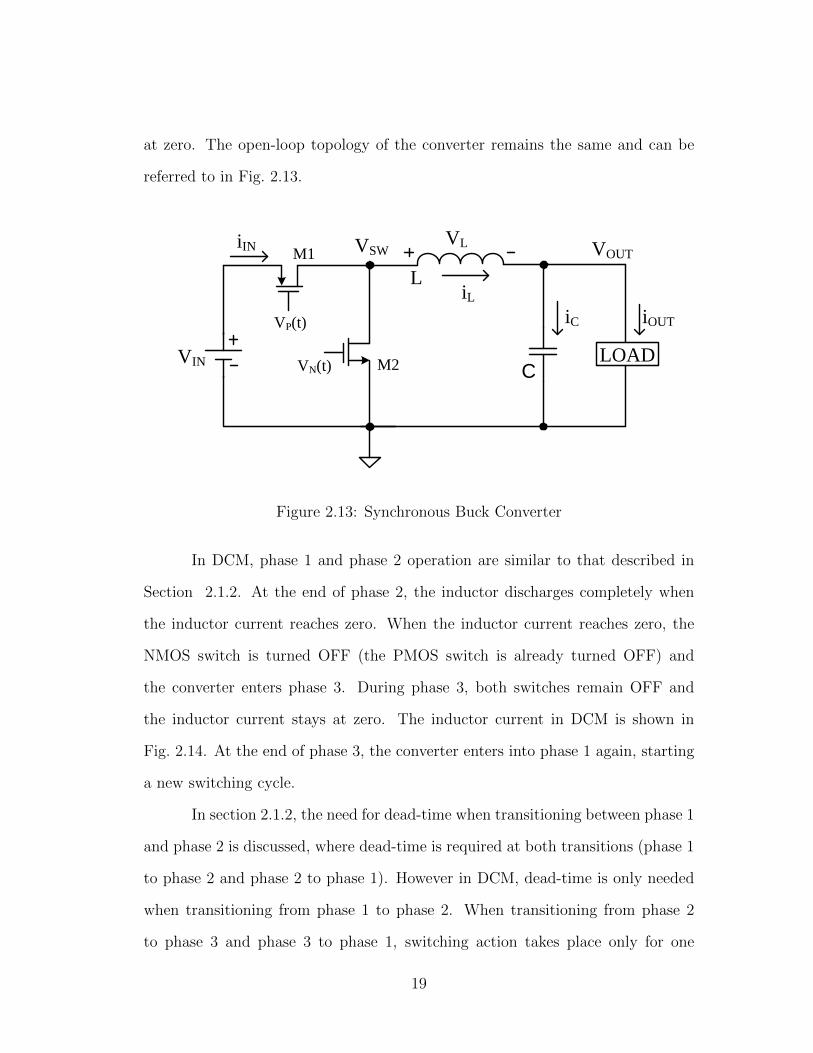
2.13 Synchronous Buck Converter . . . . . . . . . . . . . . . . . . . . . 19
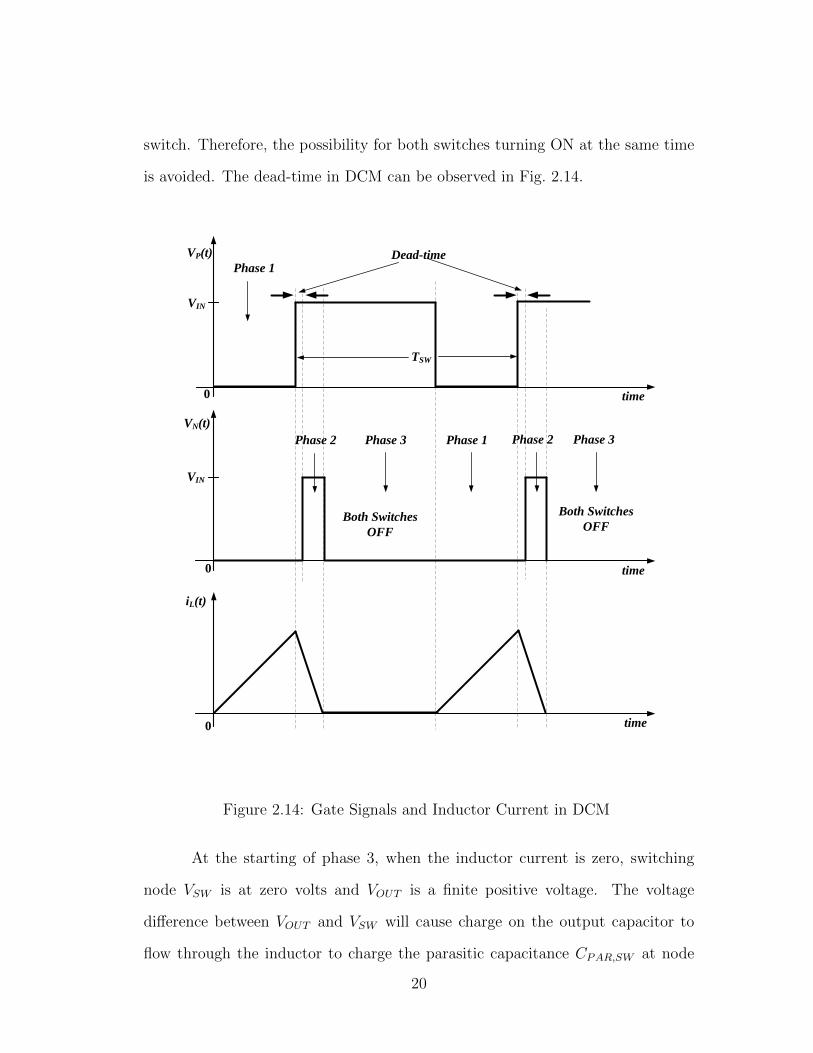
2.14 Gate Signals and Inductor Current in DCM . . . . . . . . . . . . 20
2.15 Switching node with ringing . . . . . . . . . . . . . . . . . . . . . 21
2.16 Implementation of PFM mode controller from [2] . . . . . . . . . 23
2.17 Implementation of retention mode controller from [2] . . . . . . . 25
2.18 Implementation of PFM controller from [3] . . . . . . . . . . . . . 26
xii
2.19 Implementation of of ST-ZCD [3] . . . . . . . . . . . . . . . . . . 27
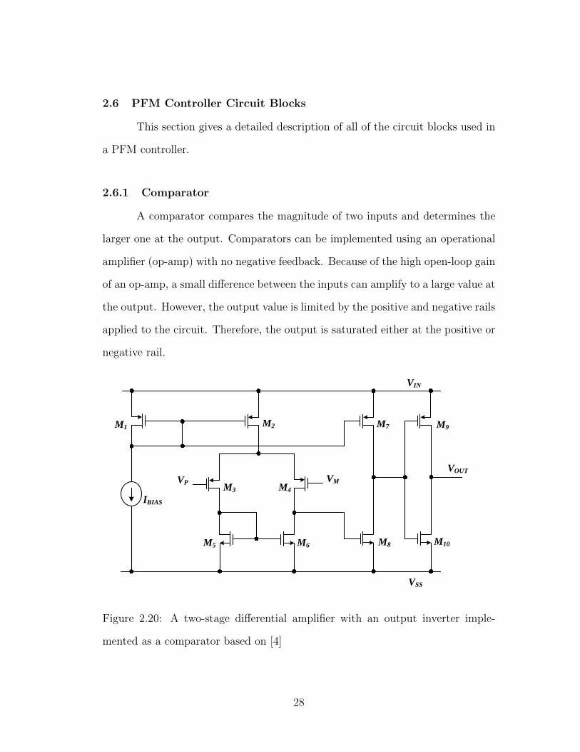
2.20 A two-stage differential amplifier with an output inverter imple-mented as a comparator based on [4] . . . . . . . . . . . . . . . . 28
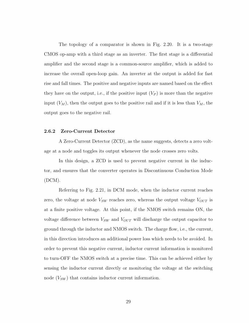
2.21 Synchronous Buck Converter . . . . . . . . . . . . . . . . . . . . . 30
2.22 Three-stage comparator using common-gate differential amplifier [5] 31
2.23 S-R Latch with NOR Gates . . . . . . . . . . . . . . . . . . . . . 32
2.24 A positive-edge triggered D Flip-Flop with asynchronous-low reset 33
2.25 Current-starved delay line based on [4] . . . . . . . . . . . . . . . 34
2.26 Non-overlapping clock generator based on [4] . . . . . . . . . . . . 35
2.27 Creating Dead-Time using Non-Overlapping Clock Generator fromFig. 2.26 . . . . . . . . . . . . . . . . . . . . . . . . . . . . . . . . 37
2.28 Gate Drivers with scale factor S . . . . . . . . . . . . . . . . . . . 38
3.1 Synchronous Buck Converter in phase 1 . . . . . . . . . . . . . . . 41
3.2 Synchronous Buck Converter in phase 2 . . . . . . . . . . . . . . . 42
3.3 Synchronous Buck Converter in phase 3) . . . . . . . . . . . . . . 42
3.4 Inductor current in DCM . . . . . . . . . . . . . . . . . . . . . . . 45
3.5 Voltage and current in a capacitor . . . . . . . . . . . . . . . . . . 48
3.6 Voltage and current in a capacitor that has ESR . . . . . . . . . 49
3.7 Parasitic capacitances at the gate terminal of switches . . . . . . . 51
3.8 A Constant on-time control loop implementation . . . . . . . . . . 57
3.9 Start-up operation without start-up circuitry . . . . . . . . . . . . 61
3.10 Start-up operation with start-up circuitry . . . . . . . . . . . . . 63
3.11 Start-up when the clock misses . . . . . . . . . . . . . . . . . . . 64
3.12 D flip-flop clock misses as RST is low when the clock edge occurs 64
3.13 Start-up . . . . . . . . . . . . . . . . . . . . . . . . . . . . . . . . 65
xiii
3.14 A three-stage CMOS differential amplifier implemented as a com-parator . . . . . . . . . . . . . . . . . . . . . . . . . . . . . . . . . 66
3.15 A three-stage comparator using common-gate differential amplifier 67
3.16 A current-starved delay line . . . . . . . . . . . . . . . . . . . . . 68
3.17 A three-stage CMOS differential amplifier implemented as a com-parator . . . . . . . . . . . . . . . . . . . . . . . . . . . . . . . . . 69
3.18 Comparator Operation . . . . . . . . . . . . . . . . . . . . . . . . 70
3.19 A three-stage comparator using common-gate differential amplifier 71
3.20 Inputs and output signals of ZCD . . . . . . . . . . . . . . . . . . 73
3.21 An SR latch with NAND gates implemented as a non-overlappingclock generator . . . . . . . . . . . . . . . . . . . . . . . . . . . . 74
3.22 Dead-time generated by non-overlapping clock generator . . . . . 75
3.23 A current-starved delay line . . . . . . . . . . . . . . . . . . . . . 76
3.24 Delay from input to output . . . . . . . . . . . . . . . . . . . . . 77
4.1 Test bench for system level buck converter . . . . . . . . . . . . . 79
4.2 Output voltage and gate signals at 20 µA load current. . . . . . . 80
4.3 Inductor current and switching node at 20 µA load current. . . . 81
4.4 Output voltage and gate signals in steady-state at 20 µA load current. 82
4.5 Inductor current and switching node in steady-state at 20 µA loadcurrent. . . . . . . . . . . . . . . . . . . . . . . . . . . . . . . . . 87
4.6 Detecting zero volts at node VSW at 20 µA load current. . . . . . 88
4.7 Ringing at the switching node in phase 3 at 20 µA load current. . 89
4.8 Output voltage and gate signals in steady-state at a load currentof 200 µA. . . . . . . . . . . . . . . . . . . . . . . . . . . . . . . . 90
4.9 Switching node and inductor current in steady-state at a load cur-rent of 200 µA. . . . . . . . . . . . . . . . . . . . . . . . . . . . . 91
4.10 Load regulation testbench . . . . . . . . . . . . . . . . . . . . . . 92
xiv
4.11 Load transient response . . . . . . . . . . . . . . . . . . . . . . . 93
4.12 20 µA to 200 µA load transient . . . . . . . . . . . . . . . . . . . 94
4.13 200 µA to 20 µA load transient . . . . . . . . . . . . . . . . . . . 95
4.14 Testbench for line transient simulation . . . . . . . . . . . . . . . 96
4.15 Line transient simulation response . . . . . . . . . . . . . . . . . . 97
4.16 Line transient simulation response (3.6 V - 3.0 V) . . . . . . . . . 98
4.17 Line transient simulation response (3.0 V - 3.6 V) . . . . . . . . . 99
5.1 Complete layout of the DCM buck converter with pad frame . . . 101
5.2 Comparator layout . . . . . . . . . . . . . . . . . . . . . . . . . . 103
5.3 Zero Current Detector layout . . . . . . . . . . . . . . . . . . . . 103
5.4 Current-starved delay line . . . . . . . . . . . . . . . . . . . . . . 103
5.5 Current-starved delay line . . . . . . . . . . . . . . . . . . . . . . 104
5.6 D flip-flop . . . . . . . . . . . . . . . . . . . . . . . . . . . . . . . 104
5.7 Non-overlapping clock generator . . . . . . . . . . . . . . . . . . . 105
5.8 Output voltage ripple . . . . . . . . . . . . . . . . . . . . . . . . . 105
5.9 Output signals of non-overlapping clock generators . . . . . . . . 106
5.10 Output voltage and input signals to the gate drivers . . . . . . . . 107
5.11 Output of ZCD and the NMOS gate driver input . . . . . . . . . 107
xv
Chapter 1
INTRODUCTION
1.1 Motivation
Wearable electronic devices such as smart watches and fitness trackers have
gained vast significance over the past few years and transformed the way we live.
Smart watches have brought the power of smartphones onto a person’s wrist [6],
whereas fitness tracking wearables are used to monitor the body activity of the
person. The small size and light weight of these devices make these devices more
attractive among users.
Wearable electronics, which are portable in nature, are generally powered
by a rechargeable battery. Users do not want to recharge their batteries often,
which will demand these devices to have longer battery run time (time to drain
a fully charged battery before needing to recharge it). Fitness tracking devices,
which are always carried by the users so that the body activity is monitored
round the clock, requires the battery to run continually. However, the small sizes
of these devices also limits the battery size, which thereby limits the battery
energy. In order to achieve long battery run time with the battery running all the
time and with limited battery energy, an efficient energy management system is
required. Increasing the battery life is not the only solution. There are alternative
ways to supplement the battery, such as energy harvesting or wireless charging [7].
Regardless, designing an efficient energy management system can reduce the power
1
delivered from the battery, which thereby increases the time between successive
recharges.
The rechargeable batteries that are used in these devices have a fixed volt-
age range. However, the functional blocks integrated in these devices work under
different voltage domains and also have unique current requirements. Therefore,
voltage regulators, which convert the input battery voltage to different DC volt-
ages, are required for each voltage domain. Apart from the DC-DC conversion, the
efficient management of battery power is also determined by the DC-DC voltage
regulators. Therefore, all the voltage regulators together form a power manage-
ment system.
Voltage regulators are primarily classified as linear regulators and switching
regulators. A Low Drop-Out regulator (LDO) is a linear regulator, which is highly
efficient if the output voltage is close to the input voltage. However, an LDO will
lose its efficiency if the input to output voltage ratio increases. Switched-capacitor
and inductor-based converters fall under switching regulators, which are highly
efficient for any voltage conversion ratio. Inductor-based converters are preferred
over switched-capacitor converters, because of their better efficiency over wide
load current and input voltage range. The main disadvantage of the inductor-
based switching regulator is that the passive components, such as the inductor
and capacitor, consume more board area.
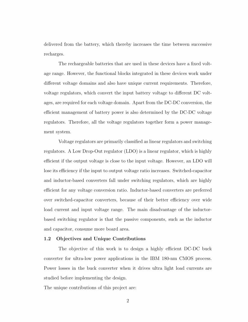
1.2 Objectives and Unique Contributions
The objective of this work is to design a highly efficient DC-DC buck
converter for ultra-low power applications in the IBM 180-nm CMOS process.
Power losses in the buck converter when it drives ultra light load currents are
studied before implementing the design.
The unique contributions of this project are:
2

1. Implemented the first DCM-mode synchronous buck converter at NMSU.
2. Implemented a highly efficient DC-DC buck converter for ultra-low power ap-
plications.
1.3 Report Organization
This technical report is organized into five chapters as follows.
Chapter 2 provides the literature review, where the basic operation of
the buck converter and the conventional control mechanisms used with the buck
converter are discussed. Published work on ultra-low power applications and sub-
circuit blocks used in the proposed design are also discussed here.
Chapter 3 includes the design of the buck converter, which includes the
derivations for calculating the inductor and capacitor values. This chapter also
describes the proposed control mechanism and the simulated results of the sub-
circuit blocks.
Chapter 4 presents the system-level simulation results at various load cur-
rents.
Chapter 5 shows the layout and presents the hardware measurement re-
sults. The layout techniques used and the area consumed by different blocks are
discussed.
Chapter 6 summarizes the proposed work and the results are compared
with other published work. Finally, the outstanding issues in this design are
analyzed.
3

Chapter 2
LITERATURE REVIEW
Ultra-low power applications, such as wearable medical devices, are widely used,
and their use is increasing exponentially. These devices should function contin-
uously, meaning, all the time, to achieve their purpose. The continuous func-
tionality demands more power from the battery and reduces battery run time.
Therefore, power from the battery should be used efficiently.
The aim of this chapter is to review inductor-based DC - DC buck con-
verters from the literature for ultra-light loads.
2.1 DC-DC Buck Converter
A DC-DC buck converter is a switching regulator that steps down a DC
input voltage to a lower DC output voltage. This section describes the steady-state
operation of a DC - DC buck converter, and the difference between conventional
and synchronous topologies.
2.1.1 Conventional DC-DC Buck Converter
This section gives an understanding of the operation of conventional inductor-
based buck converter in steady-state.
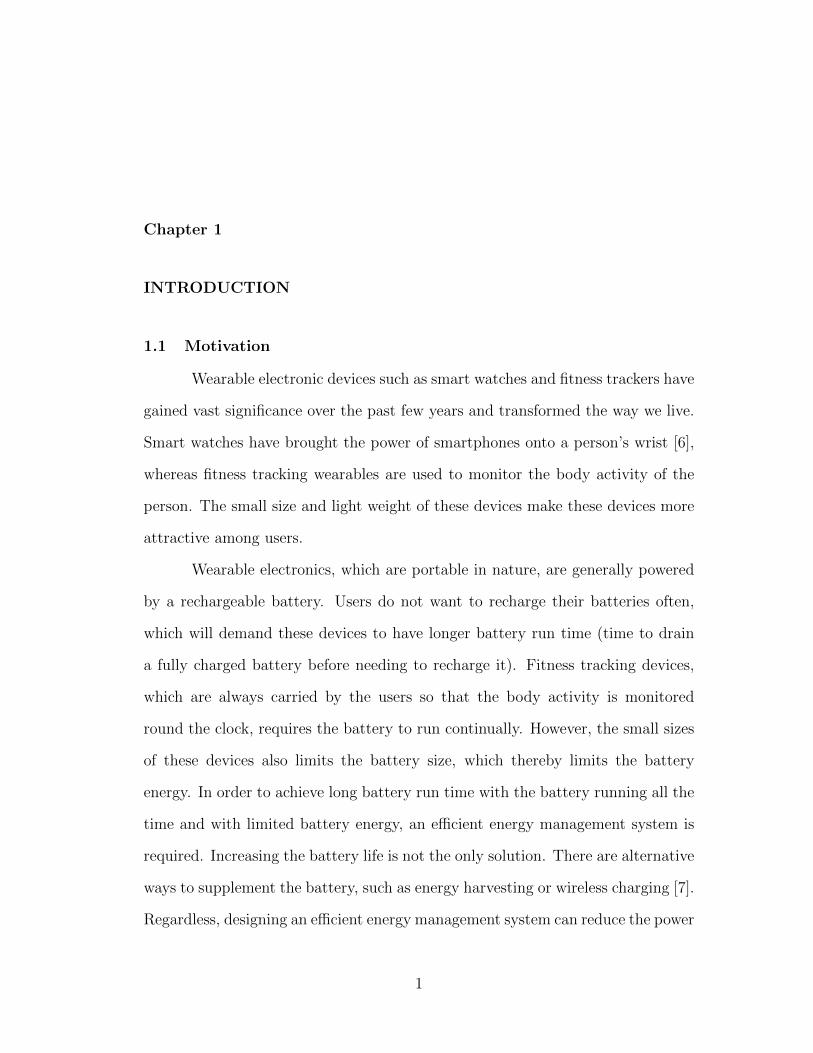
The open-loop topology of a conventional DC-DC buck converter is shown
in Fig. 2.1, in which the switch, diode, inductor and capacitor together form the
power stage and the load is powered from the power stage. The switch, which
4
is implemented as a MOSFET, is controlled by an external signal VP (t), whereas
the diode inherently acts as a switch without any external control.
iOUT
VIN
iL
VD
iIN
iC
LOAD
L
C
VSW
VLVOUT
VP(t)iD
Switch
+
Figure 2.1: Conventional Inductor-based Buck Converter
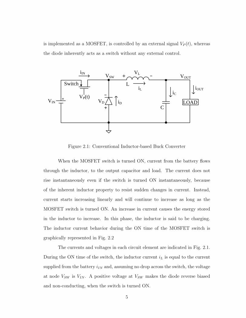
When the MOSFET switch is turned ON, current from the battery flows
through the inductor, to the output capacitor and load. The current does not
rise instantaneously even if the switch is turned ON instantaneously, because
of the inherent inductor property to resist sudden changes in current. Instead,
current starts increasing linearly and will continue to increase as long as the
MOSFET switch is turned ON. An increase in current causes the energy stored
in the inductor to increase. In this phase, the inductor is said to be charging.
The inductor current behavior during the ON time of the MOSFET switch is
graphically represented in Fig. 2.2
The currents and voltages in each circuit element are indicated in Fig. 2.1.
During the ON time of the switch, the inductor current iL is equal to the current
supplied from the battery iIN and, assuming no drop across the switch, the voltage
at node VSW is VIN . A positive voltage at VSW makes the diode reverse biased
and non-conducting, when the switch is turned ON.
5
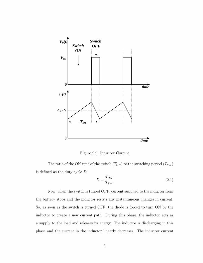
iL(t)
< iL >
time
TSW
VP(t)
time
Switch
ON
Switch
OFF
VIN
0
0
Figure 2.2: Inductor Current
The ratio of the ON time of the switch (TON) to the switching period (TSW )
is defined as the duty cycle D
D ≡ TON
TSW(2.1)
Now, when the switch is turned OFF, current supplied to the inductor from
the battery stops and the inductor resists any instantaneous changes in current.
So, as soon as the switch is turned OFF, the diode is forced to turn ON by the
inductor to create a new current path. During this phase, the inductor acts as
a supply to the load and releases its energy. The inductor is discharging in this
phase and the current in the inductor linearly decreases. The inductor current
6
behavior during the OFF time of the MOSFET switch is graphically represented
in Fig. 2.2.
During the OFF time, the voltage at node VSW is pulled to –VD to make
the diode forward-biased. The diode starts conducting at this time and the diode
current iD is equal to the inductor current iL.
In Continuous Conduction Mode (CCM) and Boundary Conduction Mode
(BCM) (described in Section 2.2), the switching cycle ends just before turning the
MOSFET switch ON again. When in steady-state, the inductor current reaches
the same value at the end of every switching cycle.
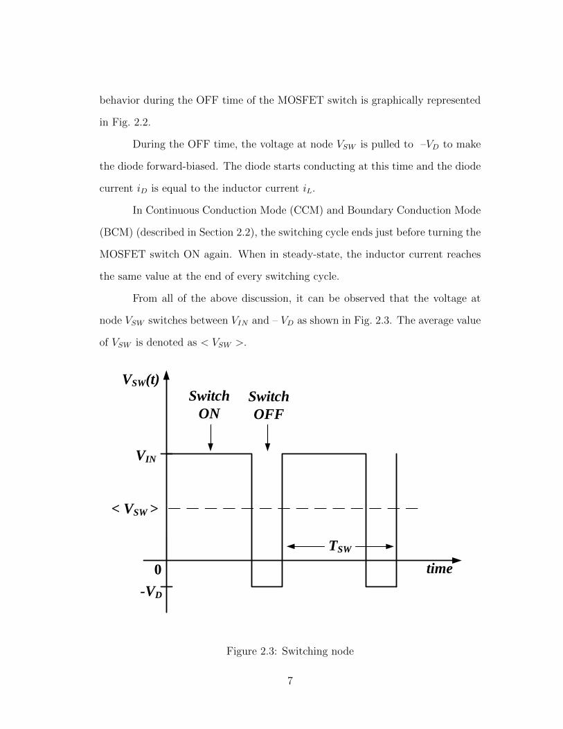
From all of the above discussion, it can be observed that the voltage at
node VSW switches between VIN and – VD as shown in Fig. 2.3. The average value
of VSW is denoted as < VSW >.
VSW(t)
< VSW >
time0
VIN
-VD
TSW
Switch
ON
Switch
OFF
Figure 2.3: Switching node
7
The high frequencies in VSW are removed by the second-order low-pass L-C
filter and the average DC value appears at VOUT [8], as
VOUT = D · VIN − (1−D) · VD (2.2)
From the above equation it can be inferred that the output voltage can be set
using the duty cycle.
The major disadvantage of this topology is the diode drop voltage of VD,
(ranging from 0.6 V–1.0 V for a silicon diode) which is significant in battery
powered devices and will limit the efficiency of the converter. Schottky diodes,
which have a lower voltage drop of 0.15 V–0.45 V, can help in improving the
converter efficiency, but this voltage drop is still considered significant. Voltage
drops in the range of 25 mV–100 mV allow the converter to achieve the highest
efficiency. This is possible by replacing the diode with a second MOSFET. The
topology is discussed in the next section.
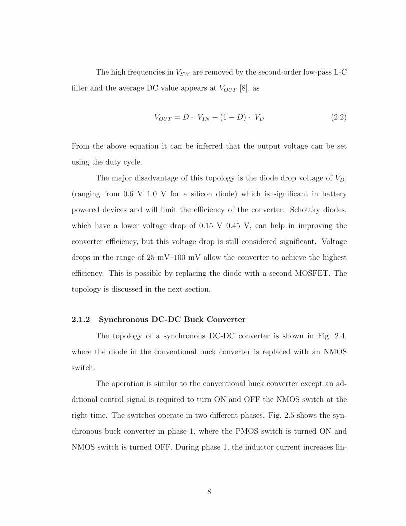
2.1.2 Synchronous DC-DC Buck Converter
The topology of a synchronous DC-DC converter is shown in Fig. 2.4,
where the diode in the conventional buck converter is replaced with an NMOS
switch.
The operation is similar to the conventional buck converter except an ad-
ditional control signal is required to turn ON and OFF the NMOS switch at the
right time. The switches operate in two different phases. Fig. 2.5 shows the syn-
chronous buck converter in phase 1, where the PMOS switch is turned ON and
NMOS switch is turned OFF. During phase 1, the inductor current increases lin-
8
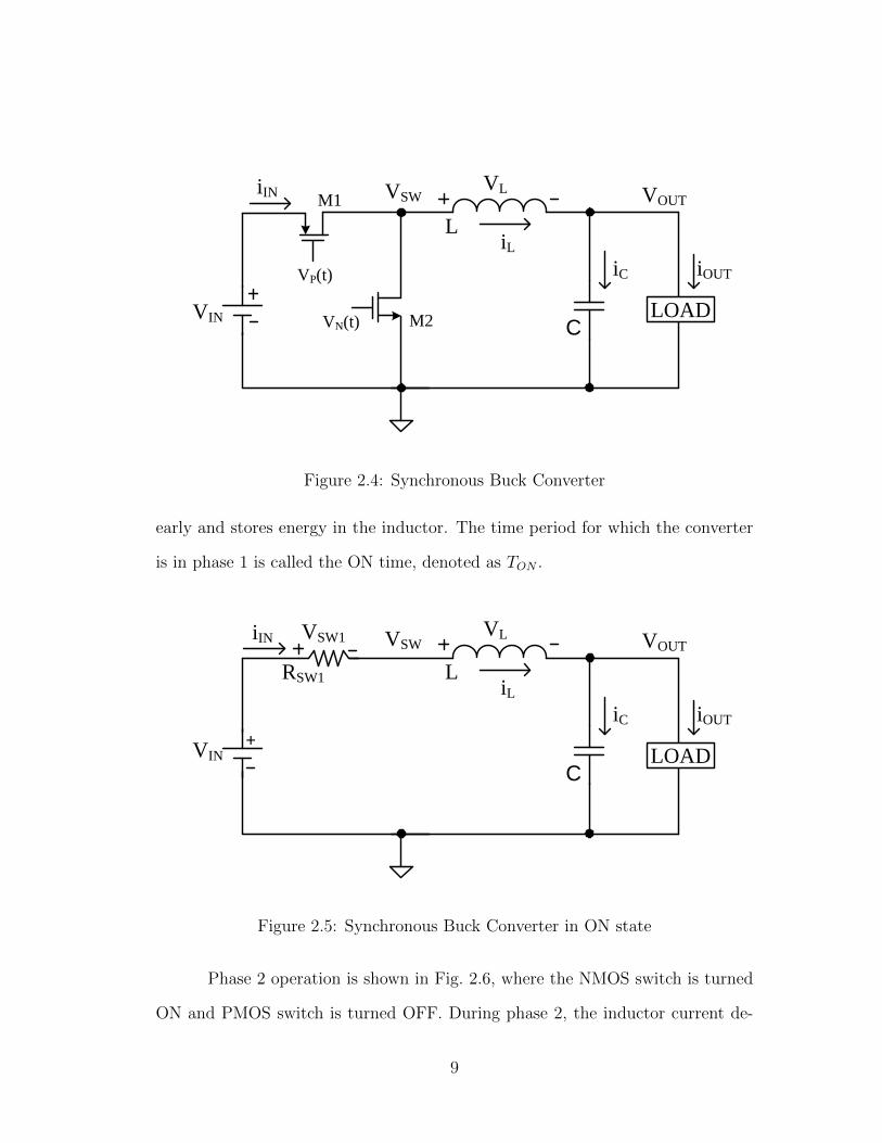
iOUT
VIN
iL
iIN
LOAD
iC
M1
M2
L
C
VP(t)
VN(t)
VL VOUTVSW
Figure 2.4: Synchronous Buck Converter
early and stores energy in the inductor. The time period for which the converter
is in phase 1 is called the ON time, denoted as TON .
iOUT
VIN
iL
iIN
LOAD
iC
L
C
VL VOUT
+
RSW1
VSW1 VSW
Figure 2.5: Synchronous Buck Converter in ON state
Phase 2 operation is shown in Fig. 2.6, where the NMOS switch is turned
ON and PMOS switch is turned OFF. During phase 2, the inductor current de-
9
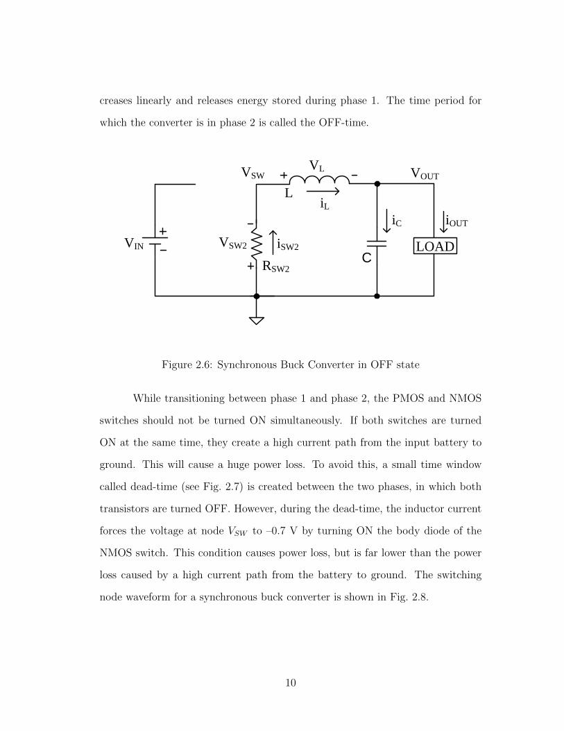
creases linearly and releases energy stored during phase 1. The time period for
which the converter is in phase 2 is called the OFF-time.
iOUT
VIN
iL
LOAD
iC
L
C
VL VOUT
VSW2
RSW2
iSW2
VSW
Figure 2.6: Synchronous Buck Converter in OFF state
While transitioning between phase 1 and phase 2, the PMOS and NMOS
switches should not be turned ON simultaneously. If both switches are turned
ON at the same time, they create a high current path from the input battery to
ground. This will cause a huge power loss. To avoid this, a small time window
called dead-time (see Fig. 2.7) is created between the two phases, in which both
transistors are turned OFF. However, during the dead-time, the inductor current
forces the voltage at node VSW to –0.7 V by turning ON the body diode of the
NMOS switch. This condition causes power loss, but is far lower than the power
loss caused by a high current path from the battery to ground. The switching
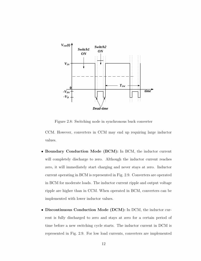
node waveform for a synchronous buck converter is shown in Fig. 2.8.
10
VN(t)
time
TSW
VP(t)
time
VIN
0
0
VIN
Dead-time
Switch1
ON
Switch2
ON
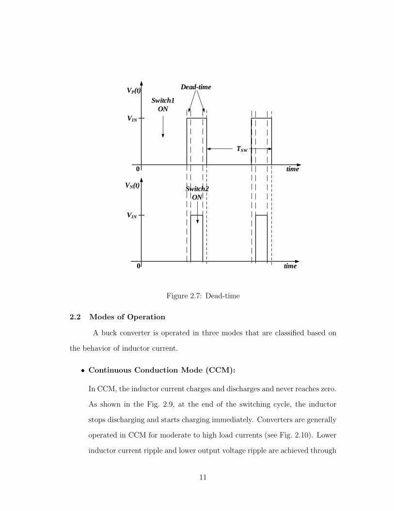
Figure 2.7: Dead-time
2.2 Modes of Operation
A buck converter is operated in three modes that are classified based on
the behavior of inductor current.
• Continuous Conduction Mode (CCM):
In CCM, the inductor current charges and discharges and never reaches zero.
As shown in the Fig. 2.9, at the end of the switching cycle, the inductor
stops discharging and starts charging immediately. Converters are generally
operated in CCM for moderate to high load currents (see Fig. 2.10). Lower
inductor current ripple and lower output voltage ripple are achieved through
11
VSW(t)
time0
VIN
-VDS
TSW
-VD
Switch1
ON
Switch2
ON
Dead-time
Figure 2.8: Switching node in synchronous buck converter
CCM. However, converters in CCM may end up requiring large inductor
values.
• Boundary Conduction Mode (BCM): In BCM, the inductor current
will completely discharge to zero. Although the inductor current reaches
zero, it will immediately start charging and never stays at zero. Inductor
current operating in BCM is represented in Fig. 2.9. Converters are operated
in BCM for moderate loads. The inductor current ripple and output voltage
ripple are higher than in CCM. When operated in BCM, converters can be
implemented with lower inductor values.
• Discontinuous Conduction Mode (DCM): In DCM, the inductor cur-
rent is fully discharged to zero and stays at zero for a certain period of
time before a new switching cycle starts. The inductor current in DCM is
represented in Fig. 2.9. For low load currents, converters are implemented
12
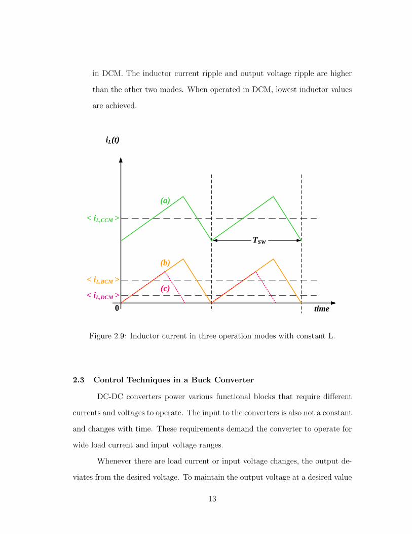
in DCM. The inductor current ripple and output voltage ripple are higher
than the other two modes. When operated in DCM, lowest inductor values
are achieved.
iL(t)
time
< iL,CCM >
TSW
0
< iL,BCM >
< iL,DCM >
(a)
(b)
(c)
Figure 2.9: Inductor current in three operation modes with constant L.
2.3 Control Techniques in a Buck Converter
DC-DC converters power various functional blocks that require different
currents and voltages to operate. The input to the converters is also not a constant
and changes with time. These requirements demand the converter to operate for
wide load current and input voltage ranges.
Whenever there are load current or input voltage changes, the output de-
viates from the desired voltage. To maintain the output voltage at a desired value
13
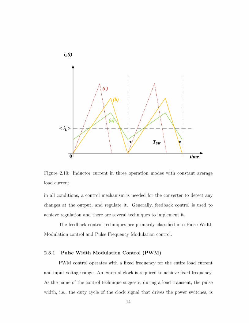
iL(t)
time
TSW
0
< iL >
(a)
(b)
(c)
Figure 2.10: Inductor current in three operation modes with constant average
load current.
in all conditions, a control mechanism is needed for the converter to detect any
changes at the output, and regulate it. Generally, feedback control is used to
achieve regulation and there are several techniques to implement it.
The feedback control techniques are primarily classified into Pulse Width
Modulation control and Pulse Frequency Modulation control.
2.3.1 Pulse Width Modulation Control (PWM)
PWM control operates with a fixed frequency for the entire load current
and input voltage range. An external clock is required to achieve fixed frequency.
As the name of the control technique suggests, during a load transient, the pulse
width, i.e., the duty cycle of the clock signal that drives the power switches, is
14
modulated to regulate the output. The duty cycle remains the same after reaching
steady-state.
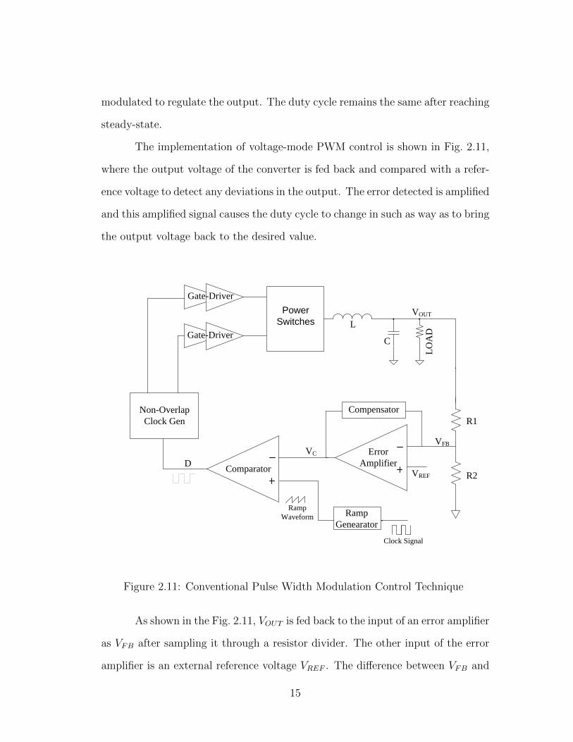
The implementation of voltage-mode PWM control is shown in Fig. 2.11,
where the output voltage of the converter is fed back and compared with a refer-
ence voltage to detect any deviations in the output. The error detected is amplified
and this amplified signal causes the duty cycle to change in such as way as to bring
the output voltage back to the desired value.
L
C
LO
AD
VREF
Error
AmplifierComparator
Non-Overlap
Clock Gen
Compensator
Ramp
Genearator
Gate-Driver
Gate-Driver
Ramp
Waveform
Clock Signal
D
VOUT
VC
VFB
R1
R2
Power
Switches
Figure 2.11: Conventional Pulse Width Modulation Control Technique
As shown in the Fig. 2.11, VOUT is fed back to the input of an error amplifier
as VFB after sampling it through a resistor divider. The other input of the error
amplifier is an external reference voltage VREF . The difference between VFB and
15
VREF is integrated across the error amplifier as VC . The fixed frequency of the
clock signal CLK is used to generate a ramp signal. The output of the error
amplifier, VC , and the ramp signal are compared to generate a pulse signal at the
comparator output. The duty cycle of this pulse signal is determined by the value
of VC . In particular, D = VC/VIN
In steady-state, VFB and VREF are equal which produces a constant VC
and therefore maintains a constant duty-cycle. For high-to-low load changes,
overshoot occurs at VOUT and this deviation in VOUT will cause VC to decrease,
thereby reducing the duty-cycle. The change in duty-cycle will bring down the
voltage at VOUT and will eventually make VFB equal to VREF when the converter
reaches steady-state.
The comparator output which contains the duty-cycle information is fed
into non-overlapping clock generators, so that two synchronous signals with dead-
time are generated to drive the MOSFET switches. Because the switches are huge
in size, the output stage of the non-overlapping clock generators could not drive
them. To increase the drive strength of the signals, gate-drivers are used.
A compensation network is needed to maintain stability of the loop. How-
ever the speed of the loop (i.e., speed at which the duty-cycle changes) is limited
by the unity-gain frequency determined by the compensation network. Therefore,
this control technique tends to have a slow transient response.
2.3.2 Pulse Frequency Modulation (PFM)
PFM is another control technique where the steady-state frequency scales
proportionally with the load current. This control technique is most often imple-
mented when the converters operate in Discontinuous Conduction Mode (DCM).
16
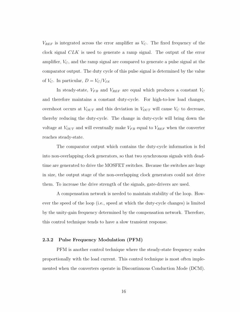
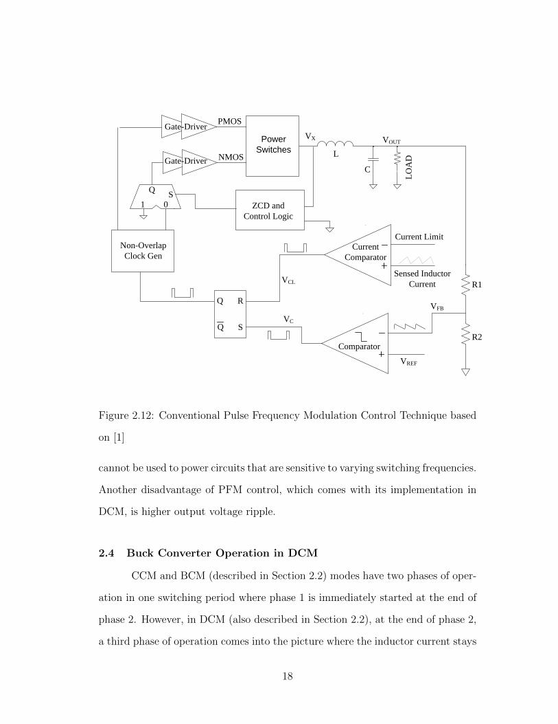
The conventional PFM control technique is shown in Fig. 2.12. The sam-
pled output voltage VFB is fed back to the comparator and compared with VREF .
Whenever VFB goes below VREF , comparator output VC goes high and sets the SR
latch to turn ON the PMOS switch. The turn-OFF decision of the PMOS switch is
determined by the current comparator, whose inputs are the sensed inductor cur-
rent and a reference current limit. When the inductor current reaches a maximum
value, the output of the current comparator VCL goes high and resets the SR latch
to turn OFF the PMOS switch. Subsequently, the NMOS switch is turned ON
after a short dead-time determined by the non-overlapping clock generators. The
turn-OFF decision of the NMOS switch is determined by the Zero-Current Detec-
tor (ZCD), which compares the switching node VX with GND. When switching
node VX crosses GND (i.e., when the inductor current reaches zero), the output
of the ZCD goes high and the NMOS switch is turned OFF. Both PMOS and
NMOS switches remain OFF until VFB again goes below VREF .
When both switches are turned OFF, the converter enters DCM where the
converter is completely OFF and there is no energy supplied from the inductor.
During this period, the inductor current stays at zero and the output capacitor
discharges to supply current to the load.
When the load current changes from high to low, the increase in load resis-
tance will cause the RC time constant at the output to increase, which translates
into a reduced discharge rate of the output capacitor. Slow discharge of the out-
put capacitor will thereby delay the turn-ON of the PMOS switch, causing the
switching frequency to decrease.
The main advantage of PFM control is that the converter can have a wide
load current range because of its property of frequency scaling proportionally with
the load. The main disadvantage of converters implemented with PFM is that they
17
L
C
LO
AD
m
Comparator
Non-Overlap
Clock Gen
Gate-Driver
Gate-Driver
VOUT
VFB
R1
R2
Power
Switches
VREF
m
RQ
SQ
VX
Current
Comparator
Sensed Inductor
Current
Current Limit
ZCD and
Control Logic
PMOS
NMOS
VC
VCL
S01
Q
Figure 2.12: Conventional Pulse Frequency Modulation Control Technique based
on [1]
cannot be used to power circuits that are sensitive to varying switching frequencies.
Another disadvantage of PFM control, which comes with its implementation in
DCM, is higher output voltage ripple.
2.4 Buck Converter Operation in DCM
CCM and BCM (described in Section 2.2) modes have two phases of oper-
ation in one switching period where phase 1 is immediately started at the end of
phase 2. However, in DCM (also described in Section 2.2), at the end of phase 2,
a third phase of operation comes into the picture where the inductor current stays
18
at zero. The open-loop topology of the converter remains the same and can be
referred to in Fig. 2.13.
iOUT
VIN
iL
iIN
LOAD
iC
M1
M2
L
C
VP(t)
VN(t)
VL VOUTVSW
Figure 2.13: Synchronous Buck Converter
In DCM, phase 1 and phase 2 operation are similar to that described in
Section 2.1.2. At the end of phase 2, the inductor discharges completely when
the inductor current reaches zero. When the inductor current reaches zero, the
NMOS switch is turned OFF (the PMOS switch is already turned OFF) and
the converter enters phase 3. During phase 3, both switches remain OFF and
the inductor current stays at zero. The inductor current in DCM is shown in
Fig. 2.14. At the end of phase 3, the converter enters into phase 1 again, starting
a new switching cycle.
In section 2.1.2, the need for dead-time when transitioning between phase 1
and phase 2 is discussed, where dead-time is required at both transitions (phase 1
to phase 2 and phase 2 to phase 1). However in DCM, dead-time is only needed
when transitioning from phase 1 to phase 2. When transitioning from phase 2
to phase 3 and phase 3 to phase 1, switching action takes place only for one
19
switch. Therefore, the possibility for both switches turning ON at the same time
is avoided. The dead-time in DCM can be observed in Fig. 2.14.
VN(t)
time
TSW
VP(t)
time
VIN
0
0
VIN
Dead-time
iL(t)
time0
Both Switches
OFF
Phase 1
Phase 2 Phase 3 Phase 1 Phase 2 Phase 3
Both Switches
OFF
Figure 2.14: Gate Signals and Inductor Current in DCM
At the starting of phase 3, when the inductor current is zero, switching
node VSW is at zero volts and VOUT is a finite positive voltage. The voltage
difference between VOUT and VSW will cause charge on the output capacitor to
flow through the inductor to charge the parasitic capacitance CPAR,SW at node
20
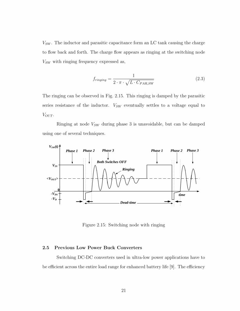
VSW . The inductor and parasitic capacitance form an LC tank causing the charge
to flow back and forth. The charge flow appears as ringing at the switching node
VSW with ringing frequency expressed as,
fringing =1
2 · π ·√L · CPAR,SW
(2.3)
The ringing can be observed in Fig. 2.15. This ringing is damped by the parasitic
series resistance of the inductor. VSW eventually settles to a voltage equal to
VOUT .
Ringing at node VSW during phase 3 is unavoidable, but can be damped
using one of several techniques.
VSW(t)
time
0
VIN
-VDS
-VD
Phase 1 Phase 2
Dead-time
Ringing
<VOUT>
Phase 3
Both Switches OFF
Phase 1 Phase 2 Phase 3
Figure 2.15: Switching node with ringing
2.5 Previous Low Power Buck Converters
Switching DC-DC converters used in ultra-low power applications have to
be efficient across the entire load range for enhanced battery life [9]. The efficiency
21
of a DC-DC converter according to [10] is given as
η ≡ POUT
PIN
(2.4)
where
PIN = POUT + PLOSS (2.5)
and
PLOSS = Pconduction + Pswitching + Pcontroller (2.6)
Power losses in a buck converter are primarily classified into conduction
losses, switching losses and quiescent (i.e., controller) losses [10]. When all of these
losses are minimized, the converter is designed to achieve the highest efficiency at a
specific load current. However, over a wide load range, efficiency of the converter
will vary. As the load current goes low, conduction losses will scale down but
controller and switching losses will remain constant [11], assuming PWM control.
Therefore, at low load currents, controller and switching losses will dominate and
degrade the efficiency of the converter.
Scaling switching frequency with load current will minimize switching losses,
which improves efficiency at light loads. This can be achieved through the PFM
control technique which is implemented in [2, 3]. If the converter is operated in
CCM at light loads, reverse inductor current will degrade the efficiency. Therefore,
converters are operated in DCM at light loads.
The work in [2], which is designed for IOT/wearable applications, uses a
DCM enabled PFM control technique at light loads (500 µA to 10 mA). As shown
in Fig. 2.16, the PFM control consists of two comparators, one-shot triggers, an
SR latch and a Zero Current Detector (ZCD). One of the comparators makes the
22
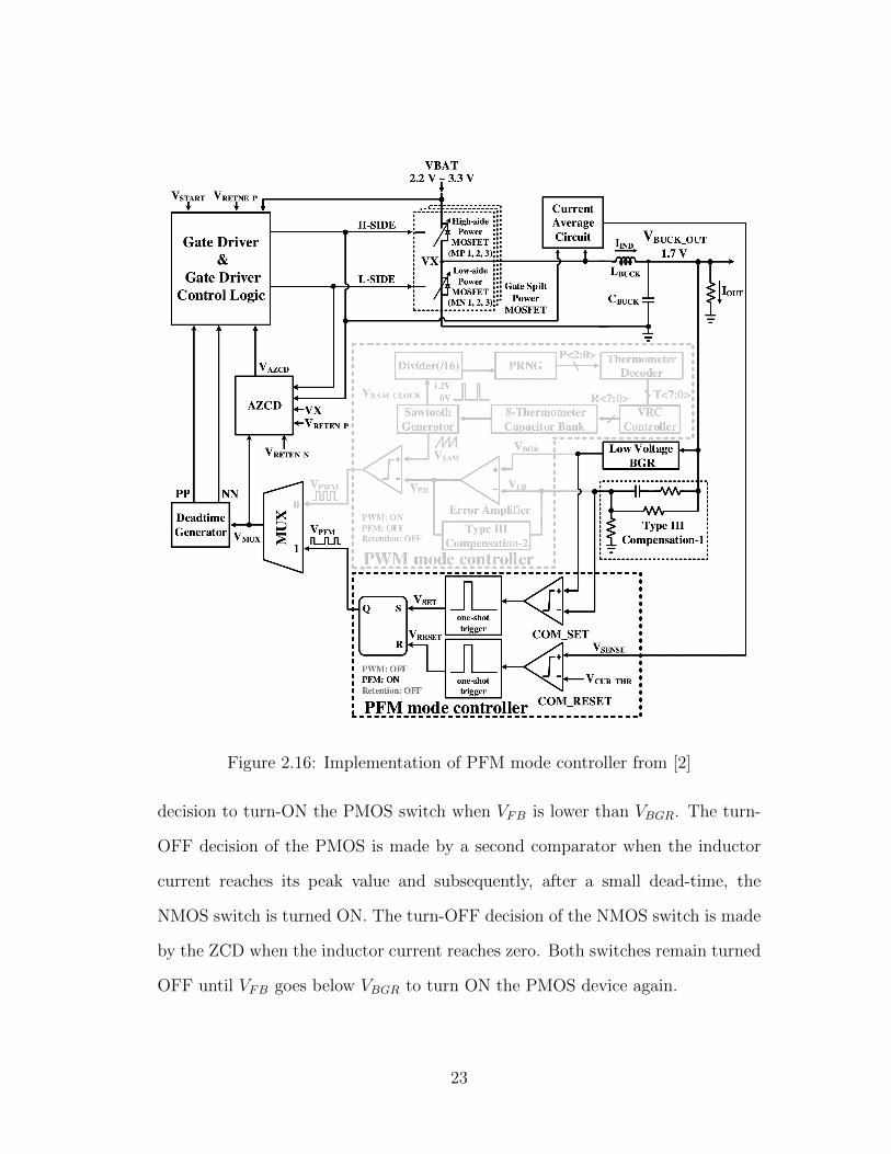
Figure 2.16: Implementation of PFM mode controller from [2]
decision to turn-ON the PMOS switch when VFB is lower than VBGR. The turn-
OFF decision of the PMOS is made by a second comparator when the inductor
current reaches its peak value and subsequently, after a small dead-time, the
NMOS switch is turned ON. The turn-OFF decision of the NMOS switch is made
by the ZCD when the inductor current reaches zero. Both switches remain turned
OFF until VFB goes below VBGR to turn ON the PMOS device again.
23
As the load current goes low, the increase in load resistance will reduce
the discharge rate of the output capacitor which will delay the turn-ON event of
the PMOS transistor. The delay in the turn-ON event of the PMOS transistor
translates into an increased switching period and reduced switching frequency.
The efficiency of the converter is further increased by reducing the current
consumption in the controller. To reduce the power consumption in the Zero
Current Detector, an Adaptive Zero Current Detector is implemented which turns
ON only when the switching node VX is negative and turns OFF immediately after
the NMOS is turned OFF. Power consumption is reduced because the turn-ON
duration of the ZCD is reduced. However, the other two comparators are ON all
the time and will consume a significant amount of power.
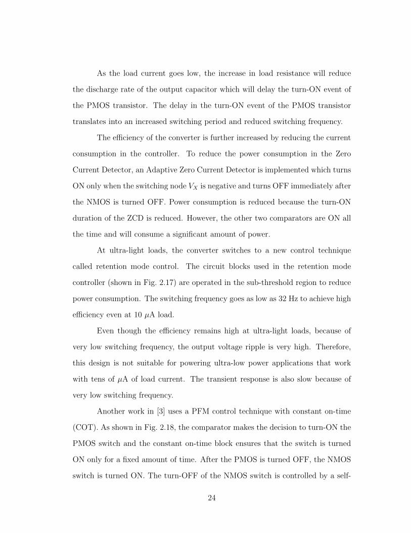
At ultra-light loads, the converter switches to a new control technique
called retention mode control. The circuit blocks used in the retention mode
controller (shown in Fig. 2.17) are operated in the sub-threshold region to reduce
power consumption. The switching frequency goes as low as 32 Hz to achieve high
efficiency even at 10 µA load.
Even though the efficiency remains high at ultra-light loads, because of
very low switching frequency, the output voltage ripple is very high. Therefore,
this design is not suitable for powering ultra-low power applications that work
with tens of µA of load current. The transient response is also slow because of
very low switching frequency.
Another work in [3] uses a PFM control technique with constant on-time
(COT). As shown in Fig. 2.18, the comparator makes the decision to turn-ON the
PMOS switch and the constant on-time block ensures that the switch is turned
ON only for a fixed amount of time. After the PMOS is turned OFF, the NMOS
switch is turned ON. The turn-OFF of the NMOS switch is controlled by a self-
24
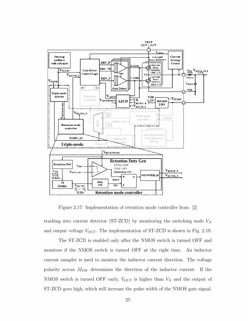
Figure 2.17: Implementation of retention mode controller from [2]
tracking zero current detector (ST-ZCD) by monitoring the switching node VX
and output voltage VOUT . The implementation of ST-ZCD is shown in Fig. 2.19.
The ST-ZCD is enabled only after the NMOS switch is turned OFF and
monitors if the NMOS switch is turned OFF at the right time. An inductor
current sampler is used to monitor the inductor current direction. The voltage
polarity across MFW determines the direction of the inductor current. If the
NMOS switch is turned OFF early, VOUT is higher than VX and the output of
ST-ZCD goes high, which will increase the pulse width of the NMOS gate signal.
25
Figure 2.18: Implementation of PFM controller from [3]
If the NMOS is turned OFF too early, VX is higher than VOUT and the output
of the ST-ZCD goes low to decrease the pulse width of the NMOS gate. The
output of the ST-ZCD toggles between high and low and adaptively determines
the appropriate pulse width.
Implementation of PFM control will cause the switching frequency to scale
down with load, thereby increasing efficiency at low loads. ST-ZCD and the
OFF-time controller are implemented digitally to reduce power consumption in
the controller. To achieve high efficiency even at ultra light loads, the control
technique switches to asynchronous mode. In asynchronous mode, the NMOS
switch is completely turned OFF and during the OFF-time, the inductor current
is conducted by the body diode of the NMOS switch. The forward voltage drop of
the diode will cause more conduction loss, but disabling the ST-ZCD and OFF-
time controller will significantly reduce the controller loss and improve overall
efficiency.
26
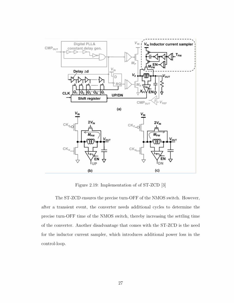
Figure 2.19: Implementation of of ST-ZCD [3]
The ST-ZCD ensures the precise turn-OFF of the NMOS switch. However,
after a transient event, the converter needs additional cycles to determine the
precise turn-OFF time of the NMOS switch, thereby increasing the settling time
of the converter. Another disadvantage that comes with the ST-ZCD is the need
for the inductor current sampler, which introduces additional power loss in the
control-loop.
27
2.6 PFM Controller Circuit Blocks
This section gives a detailed description of all of the circuit blocks used in
a PFM controller.
2.6.1 Comparator
A comparator compares the magnitude of two inputs and determines the
larger one at the output. Comparators can be implemented using an operational
amplifier (op-amp) with no negative feedback. Because of the high open-loop gain
of an op-amp, a small difference between the inputs can amplify to a large value at
the output. However, the output value is limited by the positive and negative rails
applied to the circuit. Therefore, the output is saturated either at the positive or
negative rail.
VIN
VSS
VP VM
M1 M2
M3 M4
M5 M6
M7
M8
M9
M10
VOUT
IBIAS
Figure 2.20: A two-stage differential amplifier with an output inverter imple-
mented as a comparator based on [4]
28
The topology of a comparator is shown in Fig. 2.20. It is a two-stage
CMOS op-amp with a third stage as an inverter. The first stage is a differential
amplifier and the second stage is a common-source amplifier, which is added to
increase the overall open-loop gain. An inverter at the output is added for fast
rise and fall times. The positive and negative inputs are named based on the effect
they have on the output, i.e., if the positive input (VP ) is more than the negative
input (VM), then the output goes to the positive rail and if it is less than VM , the
output goes to the negative rail.
2.6.2 Zero-Current Detector
A Zero-Current Detector (ZCD), as the name suggests, detects a zero volt-
age at a node and toggles its output whenever the node crosses zero volts.
In this design, a ZCD is used to prevent negative current in the induc-
tor, and ensures that the converter operates in Discontinuous Conduction Mode
(DCM).
Referring to Fig. 2.21, in DCM mode, when the inductor current reaches
zero, the voltage at node VSW reaches zero, whereas the output voltage VOUT is
at a finite positive voltage. At this point, if the NMOS switch remains ON, the
voltage difference between VSW and VOUT will discharge the output capacitor to
ground through the inductor and NMOS switch. The charge flow, i.e., the current,
in this direction introduces an additional power loss which needs to be avoided. In
order to prevent this negative current, inductor current information is monitored
to turn-OFF the NMOS switch at a precise time. This can be achieved either by
sensing the inductor current directly or monitoring the voltage at the switching
node (VSW ) that contains inductor current information.
29
iOUT
VIN
iL
iIN
LOAD
iC
M1
M2
L
C
VP(t)
VN(t)
VL VOUTVSW
Figure 2.21: Synchronous Buck Converter
The topology of a ZCD is shown in Fig. 2.22. It has three cascaded stages.
The first stage is a differential amplifier with inputs at the source terminals of
M2 and M3. The second stage is a common-source amplifier, which is added to
increase the overall gain. The third stage is an inverter for faster rise and fall
times at the output. The voltage VSW is fed to input V+, while V− is at ground.
The output of the ZCD is triggered whenever VSW crosses ground.
As shown in the Fig. 2.22, voltages V+ and V− are at source terminals of
M2 and M3. Because of varying VSW , the gate-source voltages of transistors M2
and M3 are generally different and will cause different currents to flow through
M2 and M3. The current through M5 is set by the current through M2, which
is then mirrored to M4. Because of the unequal currents flowing in M3 and M4,
node A is pulled high or low and this causes the output to trigger.
Initially, in phase 2, when the NMOS switch is ON, VSW is at a small
negative voltage. At the end of phase 2, the inductor discharges fully and when
30
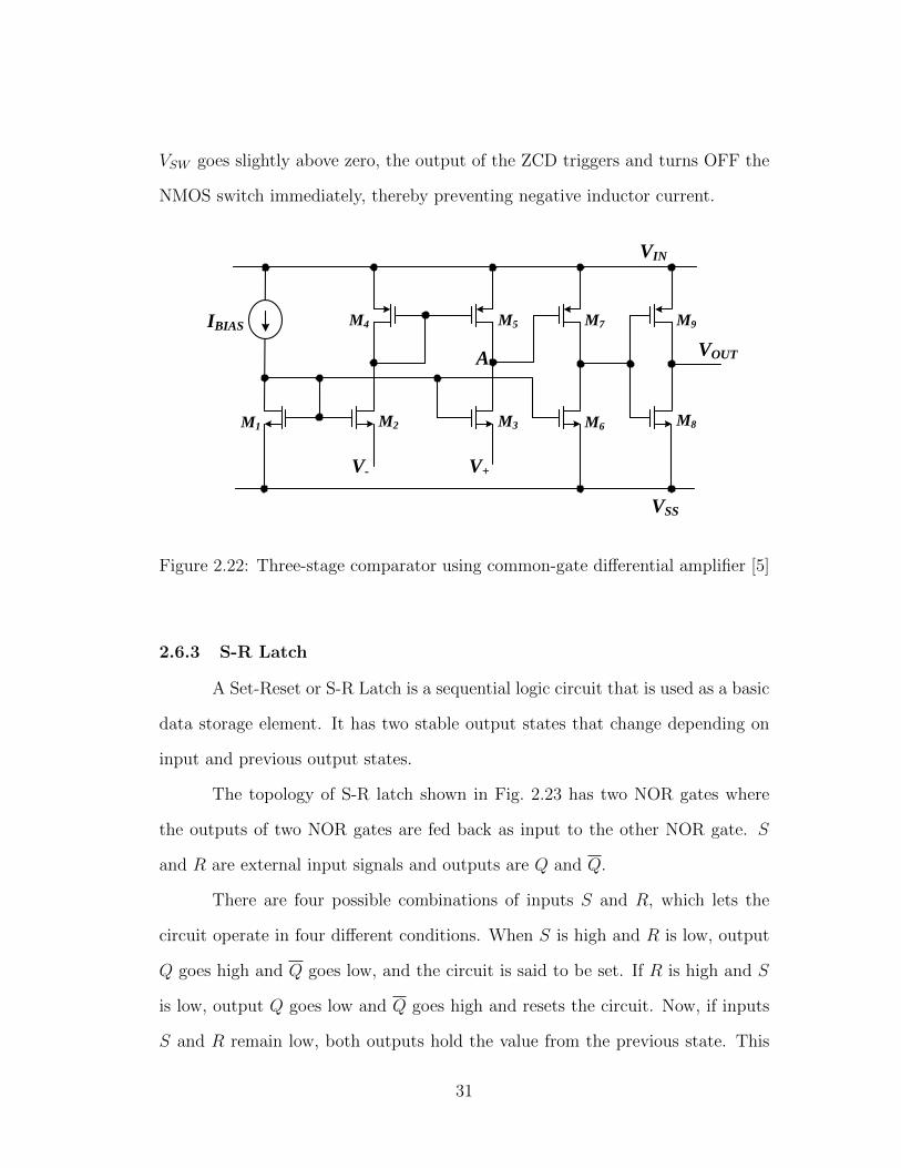
VSW goes slightly above zero, the output of the ZCD triggers and turns OFF the
NMOS switch immediately, thereby preventing negative inductor current.
M1
M4IBIAS
VIN
M2 M3
M5
V+
M6
M7
M8
M9
VSS
VOUTA
V-
Figure 2.22: Three-stage comparator using common-gate differential amplifier [5]
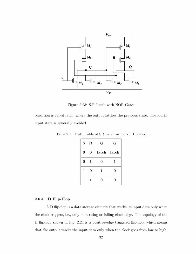
2.6.3 S-R Latch
A Set-Reset or S-R Latch is a sequential logic circuit that is used as a basic
data storage element. It has two stable output states that change depending on
input and previous output states.
The topology of S-R latch shown in Fig. 2.23 has two NOR gates where
the outputs of two NOR gates are fed back as input to the other NOR gate. S
and R are external input signals and outputs are Q and Q.
There are four possible combinations of inputs S and R, which lets the
circuit operate in four different conditions. When S is high and R is low, output
Q goes high and Q goes low, and the circuit is said to be set. If R is high and S
is low, output Q goes low and Q goes high and resets the circuit. Now, if inputs
S and R remain low, both outputs hold the value from the previous state. This
31
VSS
S
R
Q Q
M1
M2
M3 M4
M5
M6
M7 M8
VIN
Figure 2.23: S-R Latch with NOR Gates
condition is called latch, where the output latches the previous state. The fourth
input state is generally avoided.
Table 2.1: Truth Table of SR Latch using NOR Gates.
S R Q Q
0 0 latch latch
0 1 0 1
1 0 1 0
1 1 0 0
2.6.4 D Flip-Flop
A D flip-flop is a data storage element that tracks its input data only when
the clock triggers, i.e., only on a rising or falling clock edge. The topology of the
D flip-flop shown in Fig. 2.24 is a positive-edge triggered flip-flop, which means
that the output tracks the input data only when the clock goes from low to high.
32

D
clk
clk
clkclk
RST
RST
Q
Q
TG1
TG2
TG3
TG4
clk clk
clk
clk
Figure 2.24: A positive-edge triggered D Flip-Flop with asynchronous-low reset
Initially, when the clock is low, TG3 is OFF, which will block the data
at input D from passing to output Q. When clk goes from low to high, i.e.,
when a positive edge occurs, TG3 is turned ON and will pass the information at
D to Q. After the positive edge, when clk remains high, and if D changes, the
output doesn’t track the information, because TG1 is turned off. At the negative
edge, i.e., when the clock goes from high to low, because TG3 will turn OFF, the
output does not track the input. RST is active low. If it goes low, the output Q
immediately goes low and the flip-flop is reset.
2.6.5 Current-Starved Delay Line
As the name suggests, a current-starved delay line has a delay that is
controlled by currents flowing in it. The delay from the input to output of a
digital inverter circuit is determined by the NFET or PFET ON resistance and
the capacitance at its output node. If current sources are placed in series with each
transistor, the amount of current through the MOS transistors becomes limited. In
this case, the value of the current sources establishes the charging and discharging
33
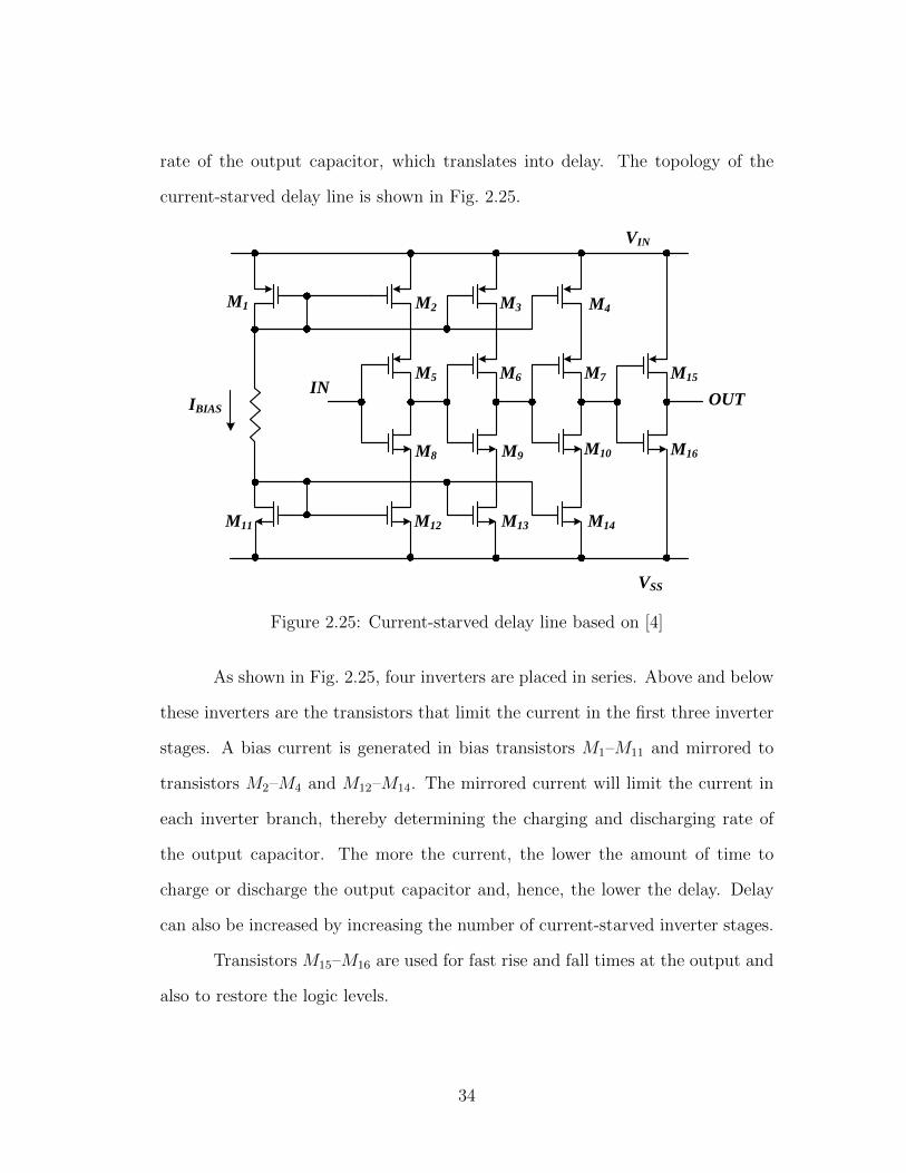
rate of the output capacitor, which translates into delay. The topology of the
current-starved delay line is shown in Fig. 2.25.
VIN
VSS
OUTIBIAS
M1 M2 M3 M4
M11 M12 M13 M14
INM5
M8
M6
M9
M7
M10
M15
M16
Figure 2.25: Current-starved delay line based on [4]
As shown in Fig. 2.25, four inverters are placed in series. Above and below
these inverters are the transistors that limit the current in the first three inverter
stages. A bias current is generated in bias transistors M1–M11 and mirrored to
transistors M2–M4 and M12–M14. The mirrored current will limit the current in
each inverter branch, thereby determining the charging and discharging rate of
the output capacitor. The more the current, the lower the amount of time to
charge or discharge the output capacitor and, hence, the lower the delay. Delay
can also be increased by increasing the number of current-starved inverter stages.
Transistors M15–M16 are used for fast rise and fall times at the output and
also to restore the logic levels.
34
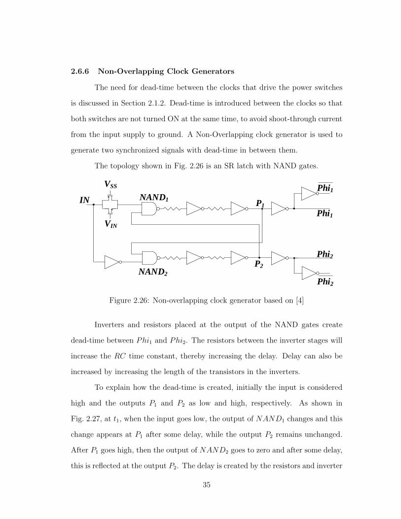
2.6.6 Non-Overlapping Clock Generators
The need for dead-time between the clocks that drive the power switches
is discussed in Section 2.1.2. Dead-time is introduced between the clocks so that
both switches are not turned ON at the same time, to avoid shoot-through current
from the input supply to ground. A Non-Overlapping clock generator is used to
generate two synchronized signals with dead-time in between them.
The topology shown in Fig. 2.26 is an SR latch with NAND gates.
IN
VIN
VSS
Phi1
Phi2
Phi1
Phi2
P1
P2
NAND1
NAND2
Figure 2.26: Non-overlapping clock generator based on [4]
Inverters and resistors placed at the output of the NAND gates create
dead-time between Phi1 and Phi2. The resistors between the inverter stages will
increase the RC time constant, thereby increasing the delay. Delay can also be
increased by increasing the length of the transistors in the inverters.
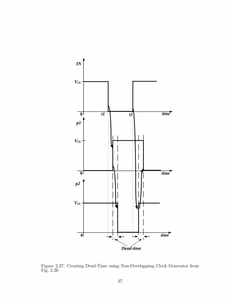
To explain how the dead-time is created, initially the input is considered
high and the outputs P1 and P2 as low and high, respectively. As shown in
Fig. 2.27, at t1, when the input goes low, the output of NAND1 changes and this
change appears at P1 after some delay, while the output P2 remains unchanged.
After P1 goes high, then the output of NAND2 goes to zero and after some delay,
this is reflected at the output P2. The delay is created by the resistors and inverter
35
stages at the output of the NAND gates. This delay creates the dead-time between
the two signals Phi1 and Phi2. When the input again goes back high at t2, P2
changes first and only after P2 changes its state, after a certain delay P1 changes
its state.
In order to achieve equal dead-time at both t1 and t2, all inverters at the
output of NAND gates should have the same size, and also all the resistors should
be of the same value.
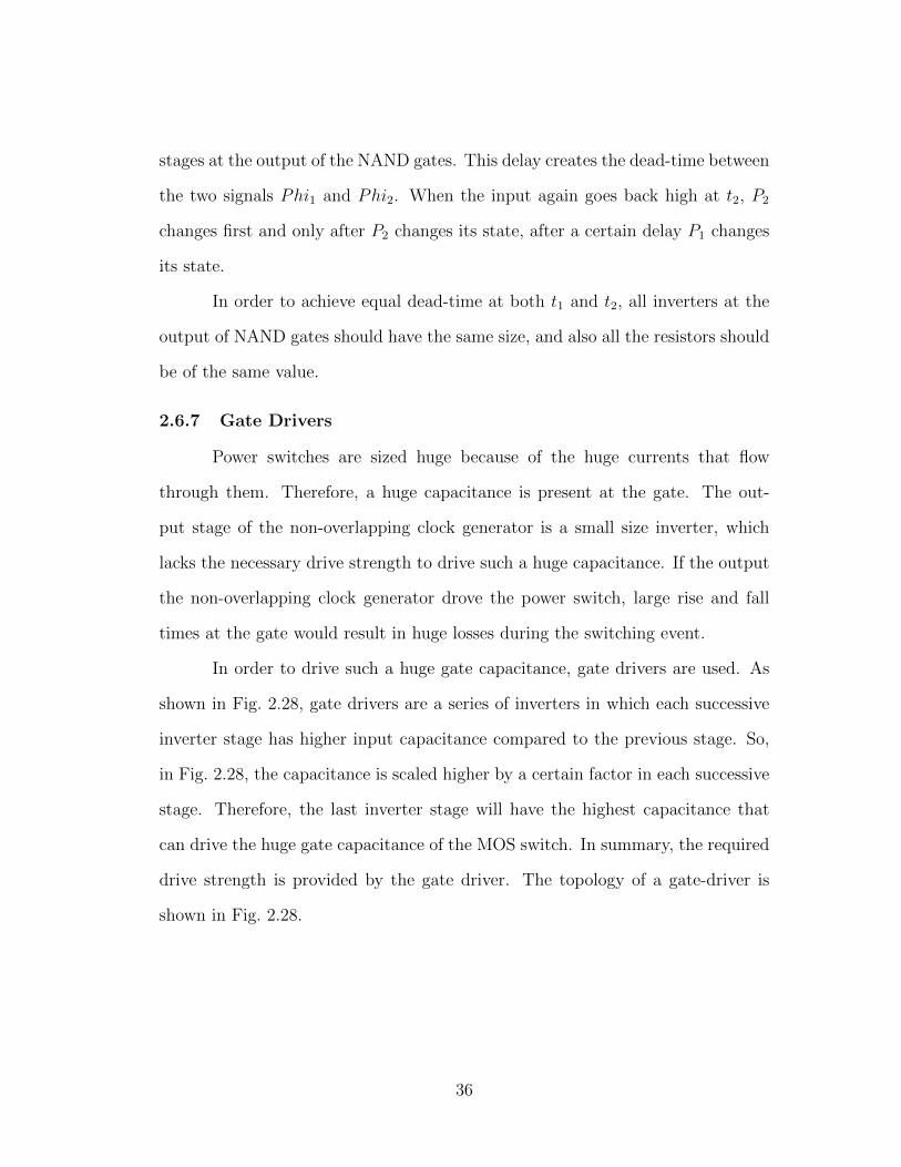
2.6.7 Gate Drivers
Power switches are sized huge because of the huge currents that flow
through them. Therefore, a huge capacitance is present at the gate. The out-
put stage of the non-overlapping clock generator is a small size inverter, which
lacks the necessary drive strength to drive such a huge capacitance. If the output
the non-overlapping clock generator drove the power switch, large rise and fall
times at the gate would result in huge losses during the switching event.
In order to drive such a huge gate capacitance, gate drivers are used. As
shown in Fig. 2.28, gate drivers are a series of inverters in which each successive
inverter stage has higher input capacitance compared to the previous stage. So,
in Fig. 2.28, the capacitance is scaled higher by a certain factor in each successive
stage. Therefore, the last inverter stage will have the highest capacitance that
can drive the huge gate capacitance of the MOS switch. In summary, the required
drive strength is provided by the gate driver. The topology of a gate-driver is
shown in Fig. 2.28.
36
p2
time
p1
time
VIN
0
0
VIN
IN
time
VIN
0
Dead-time
t2t1
Figure 2.27: Creating Dead-Time using Non-Overlapping Clock Generator fromFig. 2.26
37
IN
M1
M5
M2
M6
M3
M7
M4
M8
OUT
VIN
VSS
1 S S2 S
3
Figure 2.28: Gate Drivers with scale factor S
38

Chapter 3
DESIGN AND BLOCK-LEVEL SIMULATION RESULTS
The aim of this work is to design a highly efficient DC-DC buck converter for
ultra-low power applications.
3.1 Design Specifications and Motivation
Wearable devices are most often run by batteries because of their porta-
bility. The most widely used battery type is Li-ion because of its high energy
density. As such, the input voltage range of this design is 2.8 V – 4.2 V, which
is the voltage range of a Li-ion battery. The functional blocks in ultra-low power
applications, which consume ultra-low currents, will act as a load for the DC-DC
converter. Therefore, an ultra-low current range of 20 µA – 200 µA is chosen
for this design. The nominal operating voltage of the processor core in wearable
devices is 1.8 V [12], which is the output voltage of the converter. The output
voltage ripple should be < 2% of the output voltage to match with state-of-the-
art design constraints. To achieve high efficiency across the entire load range, the
switching frequency (fSW ) is kept variable. The targeted efficiency of this design
is 90%. Specifications of the proposed buck converter are tabulated in Table 3.1.
3.2 Buck Converter Design in Discontinuous Conduction Mode
This design is implemented using a synchronous buck converter (see Section
2.1.2) in Discontinuous Conduction Mode (DCM) operation.
With the specifications given, other parameters such as duty cycle, inductor
value and capacitor value should be calculated to complete the open-loop DC-
39
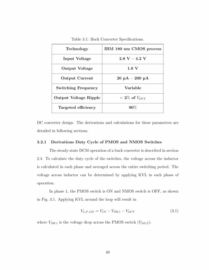
Table 3.1: Buck Converter Specifications.
Technology IBM 180 nm CMOS process
Input Voltage 2.8 V – 4.2 V
Output Voltage 1.8 V
Output Current 20 µA – 200 µA
Switching Frequency Variable
Output Voltage Ripple < 2% of VOUT
Targeted efficiency 90%
DC converter design. The derivations and calculations for these parameters are
detailed in following sections.
3.2.1 Derivations Duty Cycle of PMOS and NMOS Switches
The steady-state DCM operation of a buck converter is described in section
2.4. To calculate the duty cycle of the switches, the voltage across the inductor
is calculated in each phase and averaged across the entire switching period. The
voltage across inductor can be determined by applying KVL in each phase of
operation.
In phase 1, the PMOS switch is ON and NMOS switch is OFF, as shown
in Fig. 3.1. Applying KVL around the loop will result in
VL,P ON = VIN − VSW,1 − VOUT (3.1)
where VSW,1 is the voltage drop across the PMOS switch (VSD,P ).
40
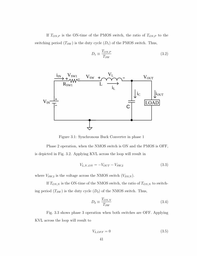
If TON,P is the ON-time of the PMOS switch, the ratio of TON,P to the
switching period (TSW ) is the duty cycle (D1) of the PMOS switch. Thus,
D1 ≡TON,P
TSW(3.2)
iOUT
VIN
iL
iIN
LOAD
iC
L
C
VL VOUT
+
RSW1
VSW1 VSW
Figure 3.1: Synchronous Buck Converter in phase 1
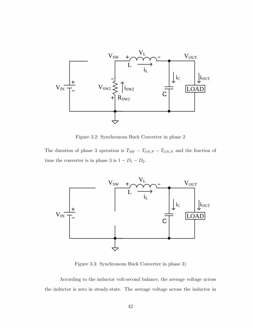
Phase 2 operation, when the NMOS switch is ON and the PMOS is OFF,
is depicted in Fig. 3.2. Applying KVL across the loop will result in
VL,N ON = −VOUT − VSW,2 (3.3)
where VSW,2 is the voltage across the NMOS switch (VDS,N).
If TON,N is the ON-time of the NMOS switch, the ratio of TON,N to switch-
ing period (TSW ) is the duty cycle (D2) of the NMOS switch. Thus,
D2 ≡TON,N
TSW(3.4)
Fig. 3.3 shows phase 3 operation when both switches are OFF. Applying
KVL across the loop will result to
VL,OFF = 0 (3.5)
41
iOUT
VIN
iL
LOAD
iC
L
C
VL VOUT
VSW2
RSW2
iSW2
VSW
Figure 3.2: Synchronous Buck Converter in phase 2
The duration of phase 3 operation is TSW − TON,P − TON,N and the fraction of
time the converter is in phase 3 is 1−D1 −D2.
iOUT
VIN
iL
LOAD
iC
L
C
VL VOUTVSW
Figure 3.3: Synchronous Buck Converter in phase 3)
According to the inductor volt-second balance, the average voltage across
the inductor is zero in steady-state. The average voltage across the inductor in
42
DCM for one switching period is expressed as
< VL >=VL,P ON ·D1 · TSW + VL,N ON ·D2 · TSW + VL,OFF · (1−D1 −D2) · TSW
TSW(3.6)
Assuming VSW,1 ≈ VSW,2 and simultaneously solving (3.6), (3.1) and (3.3) for
VOUT , we get
VOUT =VIN ·D1
D1 +D2
− VSW,1 (3.7)
where 0 < (D1 +D2) < 1 in DCM.
In (3.7), because D1/(D1 +D2) is always less than one, it can be deduced
that VOUT is always lower than VIN , which also confirms that the converter acts
as a buck converter. Given a particular value for D1 + D2 between 0 and 1, D1
can be calculated directly from (3.7).
After further solving (3.7) for D2/D1, D2 can be calculated using
D2
D1
=VIN
VOUT + VSW,1
− 1 (3.8)
3.2.2 Derivation to Calculate Inductor Value
The voltage-current (V-I) relation of an inductor with constant voltage is
expressed as
VL = L · ∆iL∆t
(3.9)
where VL is the voltage across the inductor, L is the inductance, and ∆iL is the
change in the inductor current in ∆t seconds.
In phase 1, when the PMOS switch is ON, the inductor current starts
at zero and linearly increases to reach its peak value in D1 · TSW seconds. The
difference between the peak value and its starting value is defined as the inductor
current ripple and denoted as ∆iL. In phase 1, the voltage across the inductor,
VL,P ON , is given by (3.1). Therefore, for any given switching period TSW , the V-I
43
relation of the inductor in phase 1 can be expressed as
VIN − VSW,1 − VOUT = L · ∆iLD1 · TSW
(3.10)
The above equation can be further solved for inductance L
L =(VIN − VSW,1 − VOUT ) ·D1 · TSW
∆iL(3.11)
The inductor current ripple ∆iL in terms of IOUT can be derived from
Fig. 3.4. The average value of the inductor current, as observed from Fig. 3.4, is
expressed as
< iL >=1
2· (D1 +D2) ·∆iL (3.12)
Since the output current is equal to the average inductor current (< iL >=
IOUT ), the above equation can be rewritten as
IOUT =1
2· (D1 +D2) ·∆iL (3.13)
From the above equation, ∆iL can be expressed as
∆iL =2 · IOUT
D1 +D2
(3.14)
Rewriting (3.11) by replacing ∆iL from (3.14), we get
L =(VIN − VSW,1 − VOUT ) ·D1 · TSW · (D1 +D2)
2 · IOUT
(3.15)
Therefore, for a fixed switching period (TSW ), the inductance value can be
calculated from the above equation, since the parameters VIN , VOUT and IOUT
are known values from Table 3.1. D1 and D2 values can be calculated from (3.8)
and (3.7) by assuming a particular value for D1 + D2 between 0 and 1. VSW,1 is
assumed to be approximately equal to 50 mV.
Similarly in phase 2, when the PMOS switch is OFF and the NMOS switch
is ON, the voltage across the inductor is given in (3.3). The inductor current
44
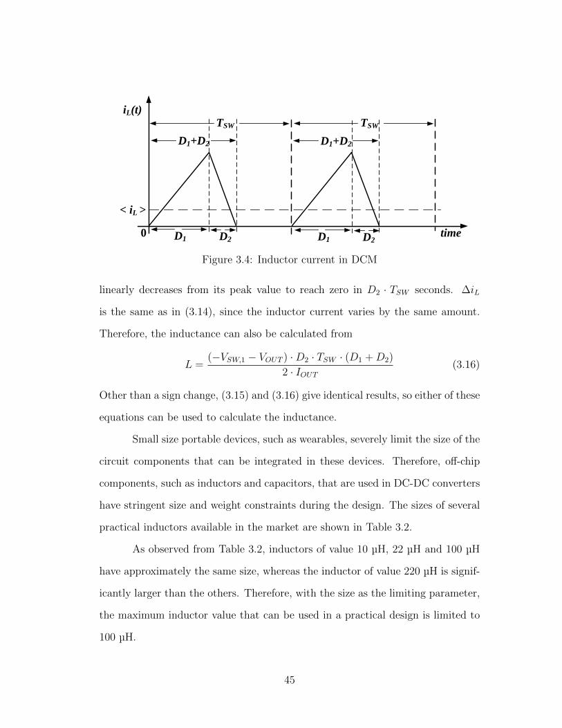
iL(t)
time0
< iL >
D1 D2
D1+D2
TSW
D1+D2
D1 D2
TSW
Figure 3.4: Inductor current in DCM
linearly decreases from its peak value to reach zero in D2 · TSW seconds. ∆iL
is the same as in (3.14), since the inductor current varies by the same amount.
Therefore, the inductance can also be calculated from
L =(−VSW,1 − VOUT ) ·D2 · TSW · (D1 +D2)
2 · IOUT
(3.16)
Other than a sign change, (3.15) and (3.16) give identical results, so either of these
equations can be used to calculate the inductance.
Small size portable devices, such as wearables, severely limit the size of the
circuit components that can be integrated in these devices. Therefore, off-chip
components, such as inductors and capacitors, that are used in DC-DC converters
have stringent size and weight constraints during the design. The sizes of several
practical inductors available in the market are shown in Table 3.2.
As observed from Table 3.2, inductors of value 10 µH, 22 µH and 100 µH
have approximately the same size, whereas the inductor of value 220 µH is signif-
icantly larger than the others. Therefore, with the size as the limiting parameter,
the maximum inductor value that can be used in a practical design is limited to
100 µH.
45
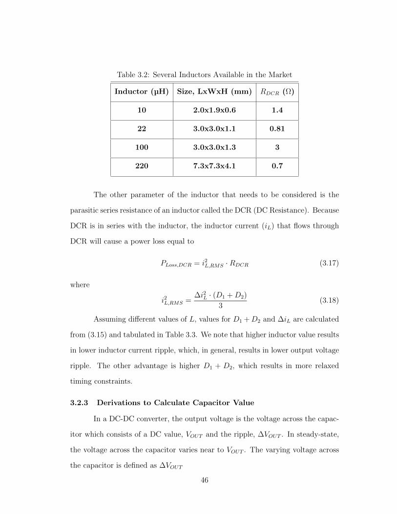
Table 3.2: Several Inductors Available in the Market
Inductor (µH) Size, LxWxH (mm) RDCR (Ω)
10 2.0x1.9x0.6 1.4
22 3.0x3.0x1.1 0.81
100 3.0x3.0x1.3 3
220 7.3x7.3x4.1 0.7
The other parameter of the inductor that needs to be considered is the
parasitic series resistance of an inductor called the DCR (DC Resistance). Because
DCR is in series with the inductor, the inductor current (iL) that flows through
DCR will cause a power loss equal to
PLoss,DCR = i2L,RMS ·RDCR (3.17)
where
i2L,RMS =∆i2L · (D1 +D2)
3(3.18)
Assuming different values of L, values for D1 +D2 and ∆iL are calculated
from (3.15) and tabulated in Table 3.3. We note that higher inductor value results
in lower inductor current ripple, which, in general, results in lower output voltage
ripple. The other advantage is higher D1 + D2, which results in more relaxed
timing constraints.
3.2.3 Derivations to Calculate Capacitor Value
In a DC-DC converter, the output voltage is the voltage across the capac-
itor which consists of a DC value, VOUT and the ripple, ∆VOUT . In steady-state,
the voltage across the capacitor varies near to VOUT . The varying voltage across
the capacitor is defined as ∆VOUT
46
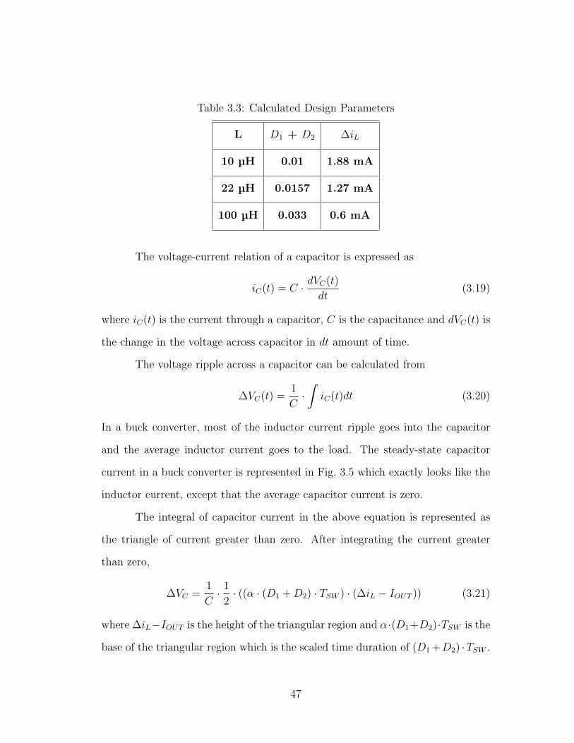
Table 3.3: Calculated Design Parameters
L D1 + D2 ∆iL
10 µH 0.01 1.88 mA
22 µH 0.0157 1.27 mA
100 µH 0.033 0.6 mA
The voltage-current relation of a capacitor is expressed as
iC(t) = C · dVC(t)
dt(3.19)
where iC(t) is the current through a capacitor, C is the capacitance and dVC(t) is
the change in the voltage across capacitor in dt amount of time.
The voltage ripple across a capacitor can be calculated from
∆VC(t) =1
C·∫iC(t)dt (3.20)
In a buck converter, most of the inductor current ripple goes into the capacitor
and the average inductor current goes to the load. The steady-state capacitor
current in a buck converter is represented in Fig. 3.5 which exactly looks like the
inductor current, except that the average capacitor current is zero.
The integral of capacitor current in the above equation is represented as
the triangle of current greater than zero. After integrating the current greater
than zero,
∆VC =1
C· 1
2· ((α · (D1 +D2) · TSW ) · (∆iL − IOUT )) (3.21)
where ∆iL−IOUT is the height of the triangular region and α·(D1+D2)·TSW is the
base of the triangular region which is the scaled time duration of (D1 +D2) ·TSW .
47
iC(t)
time0
D1+D2
TSW
D1+D2
TSW
<iL>
VOUT(t)
0
<VOUT>
time
Figure 3.5: Voltage and current in a capacitor
Parameter α is the scaling constant and can be expressed as
α =∆iL − IOUT
∆iL(3.22)
After solving (3.21) and (3.22), and since ∆VC = ∆VOUT , the output volt-
age ripple ∆VOUT is
∆VOUT =((α · (D1 +D2) · TSW ) · (∆iL − IOUT )2)
2 · C ·∆iL(3.23)
Capacitors are not ideal and every capacitor comes with a parasitic series
resistance called the Equivalent Series Resistance (ESR). The voltage across the
48
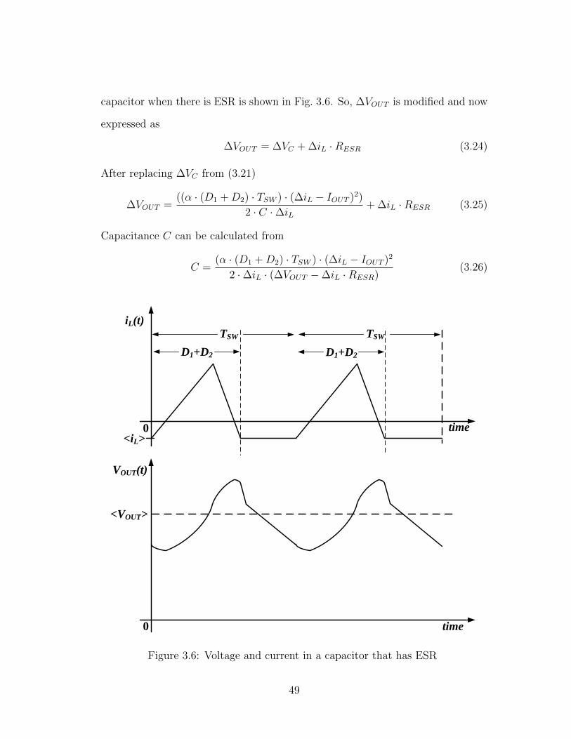
capacitor when there is ESR is shown in Fig. 3.6. So, ∆VOUT is modified and now
expressed as
∆VOUT = ∆VC + ∆iL ·RESR (3.24)
After replacing ∆VC from (3.21)
∆VOUT =((α · (D1 +D2) · TSW ) · (∆iL − IOUT )2)
2 · C ·∆iL+ ∆iL ·RESR (3.25)
Capacitance C can be calculated from
C =(α · (D1 +D2) · TSW ) · (∆iL − IOUT )2
2 ·∆iL · (∆VOUT −∆iL ·RESR)(3.26)
iL(t)
time0
D1+D2
TSW
D1+D2
TSW
<iL>
VOUT(t)
0
<VOUT>
time
Figure 3.6: Voltage and current in a capacitor that has ESR
49
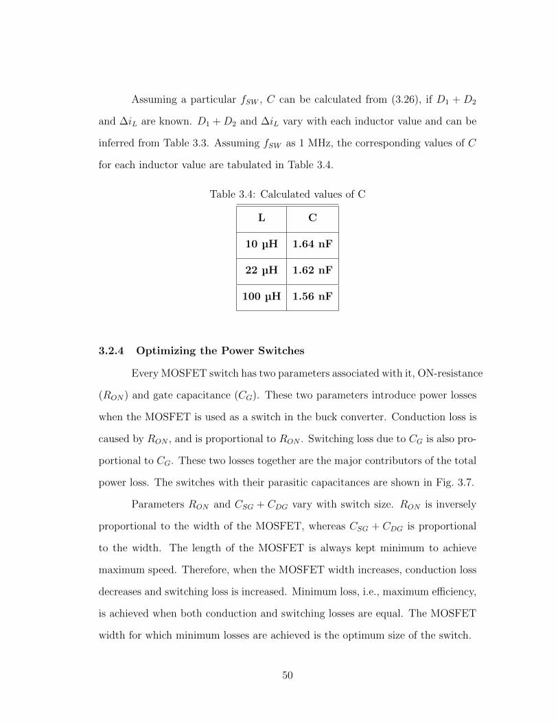
Assuming a particular fSW , C can be calculated from (3.26), if D1 + D2
and ∆iL are known. D1 +D2 and ∆iL vary with each inductor value and can be
inferred from Table 3.3. Assuming fSW as 1 MHz, the corresponding values of C
for each inductor value are tabulated in Table 3.4.
Table 3.4: Calculated values of C
L C
10 µH 1.64 nF
22 µH 1.62 nF
100 µH 1.56 nF
3.2.4 Optimizing the Power Switches
Every MOSFET switch has two parameters associated with it, ON-resistance
(RON) and gate capacitance (CG). These two parameters introduce power losses
when the MOSFET is used as a switch in the buck converter. Conduction loss is
caused by RON , and is proportional to RON . Switching loss due to CG is also pro-
portional to CG. These two losses together are the major contributors of the total
power loss. The switches with their parasitic capacitances are shown in Fig. 3.7.
Parameters RON and CSG + CDG vary with switch size. RON is inversely
proportional to the width of the MOSFET, whereas CSG + CDG is proportional
to the width. The length of the MOSFET is always kept minimum to achieve
maximum speed. Therefore, when the MOSFET width increases, conduction loss
decreases and switching loss is increased. Minimum loss, i.e., maximum efficiency,
is achieved when both conduction and switching losses are equal. The MOSFET
width for which minimum losses are achieved is the optimum size of the switch.
50
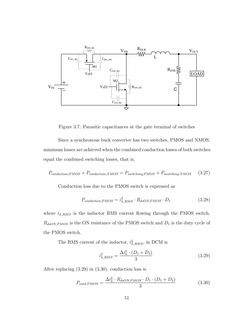
VIN
LOAD
M1
M2
L
C
VP(t)
VN(t)
VOUTVSW
CSG, M1 CDG, M1
CGD, M1
CGS, M1
RDCR
RESR
RON, M1
RON, M2
Figure 3.7: Parasitic capacitances at the gate terminal of switches
Since a synchronous buck converter has two switches, PMOS and NMOS,
minimum losses are achieved when the combined conduction losses of both switches
equal the combined switching losses, that is,
Pconduction,PMOS + Pconduction,NMOS = Pswitching,PMOS + Pswitching,NMOS (3.27)
Conduction loss due to the PMOS switch is expressed as
Pconduction,PMOS = i2L,RMS ·RdsON,PMOS ·D1 (3.28)
where iL,RMS is the inductor RMS current flowing through the PMOS switch,
RdsON,PMOS is the ON resistance of the PMOS switch and D1 is the duty cycle of
the PMOS switch.
The RMS current of the inductor, i2L,RMS, in DCM is
i2L,RMS =∆i2L · (D1 +D2)
3(3.29)
After replacing (3.29) in (3.30), conduction loss is
Pcond,PMOS =∆i2L ·RdsON,PMOS ·D1 · (D1 +D2)
3(3.30)
51
Similarly, conduction loss in the NMOS switch is
Pcond,NMOS = i2L,RMS ·RdsON,NMOS ·D2 =∆i2L ·RdsON,NMOS ·D2 · (D1 +D2)
3
(3.31)
Switching losses of a MOSFET switch can be expressed as
PSwitching,Loss = CG · fSW · ∆V 2 (3.32)
where CG is the gate capacitance that consists of the gate-source capacitance
(CGS) and gate-drain capacitance (CGD), fSW is the switching frequency and ∆V
is the change in voltage across the capacitor.
At the turn-ON event of the PMOS switch, the switching loss due to the
gate-source capacitance of the PMOS switch is
PCSGP (ON),Loss =1
2· CGS,P · fSW · V 2
IN (3.33)
and the switching loss due to the gate-drain capacitance of the PMOS is
PCDGP (ON),Loss =1
2· CDG,P · fSW · (2 · VIN − VOUT )2 (3.34)
In DCM, before the turn-ON of the PMOS switch, when both switches are turned
OFF, the switching node VSW , which is the drain terminal of the PMOS, settles
to VOUT and the gate terminal is at VIN . So, the voltage across CDG is VOUT -VIN .
After the turn-ON, VSW is approximately VIN and the gate terminal is at zero
Volts, which makes the voltage across CDG −VIN . Therefore, the change in the
voltage across the capacitor is 2 · VIN − VOUT .
At the turn-OFF event of the PMOS switch, the switching loss due to the
gate-source capacitance is
PCSGP (OFF ),Loss =1
2· CGS,P · fSW · V 2
IN (3.35)
52
The source terminal of the PMOS switch is always a constant voltage VIN .
During the turn-ON or turn-OFF event of the switch, only the gate voltage toggles
between 0 and VIN . Therefore, the voltage change across CGS during both turn-
ON and turn-OFF is VIN
The switching loss due to the gate-drain capacitance is
PCDGP (OFF ),Loss =1
2· CDG,P · fSW · (2 · VIN − VD)2 (3.36)
When the PMOS switch is ON, the gate terminal is at zero volts and the voltage
at the drain terminal, which is the switching node VSW , is VIN . So, the voltage
across CDG is VIN . After the turn-OFF, during the dead-time, the gate terminal
is at zero volts and node VSW is at -VD (body diode drop voltage) which makes
the voltage across CDG as −VD − VIN . Therefore, the voltage change across CDG
is 2 · VIN − VD.
The total switching losses due to the PMOS switch are
Pswitching,PMOS = PCSGP (ON),Loss + PCDGP (ON),Loss (3.37)
+ PCSGP (OFF ),Loss + PCDGP (OFF ),Loss
which gives
Pswitching,PMOS = CGS,P · fSW · V 2IN +
1
2· CDG,P · fSW · (2 · VIN − VOUT )2
+1
2· CDG,P · fSW · (2 · VIN − VD)2 (3.38)
For the NMOS switch, at the turn-ON event of the NMOS switch, the
switching loss due to CGS of the NMOS is
PCGSN(ON),Loss =1
2· CGS,N · fSW · V 2
IN (3.39)
53
The switching loss due to CGD,N of the NMOS is
PCGDN(ON),Loss =1
2· CGD,N · fSW · (VIN − VD)2 (3.40)
Before turning ON the NMOS switch, during the dead-time, the voltage across
CGD,N is VD because the drain terminal of the NMOS switch is -VD and the gate
terminal is zero volts. After the NMOS switch is turned ON, the drain terminal is
at zero volts and the gate is at VIN which makes the voltage across CGD,N equal
to VIN . Therefore, the voltage change across CGD,N is VIN -VD.
At the turn-OFF event of the NMOS switch, the switching loss due to
CGS,N is
PCGSN(OFF ),Loss =1
2· CGS,N · fSW · V 2
IN (3.41)
Because the source terminal of the NMOS switch is always at ground, at both
turn-ON and turn-OFF events, only the gate terminal toggles between 0 and VIN .
Therefore, the voltage change across CGS,N during both events is VIN
The switching loss due to CGD,N is
PCGDN(OFF ),Loss =1
2· CGD,N · fSW · (VIN + VOUT )2 (3.42)
Before turning OFF the NMOS switch, the voltage across CGD,N is VIN because
the drain terminal of the NMOS switch is zero volts and the gate terminal is at
VIN . After the NMOS switch is turned ON, the drain terminal settles to VOUT and
the gate is at zero volts, which makes the voltage across CGD,N equal to −VOUT .
Therefore, the voltage change across CGD,N is VIN + VOUT .
The total switching losses in the NMOS switch are
Pswitching,NMOS = PCGSN(ON),Loss + PCGDN(ON),Loss (3.43)
+ PCGSN(OFF ),Loss + PCGDN(OFF ),Loss
54
which results in
Pswitching,NMOS = CGS,N · fSW · V 2IN +
1
2· CGD,N · fSW · (VIN − VD)2
+1
2· CGD,N · fSW · (VIN + VOUT )2 (3.44)
3.2.5 Choosing the Inductor Value
As described in Section. 3.2.2, the maximum size of the inductor is limited
to 100 µH and the best inductor has to be chosen among 10 µH, 22 µH and 100
µH.
For fixed design values of L and C, the converter will achieve maximum
efficiency when (3.27) is satisfied i.e., when the combined conduction losses of both
switches equals the combined switching losses. The losses introduced by RDCR of
the inductor will also reduce the efficiency.
The open-loop converter is optimized when (3.27) is satisfied. Assuming
fSW is 1 MHz, the corresponding capacitor value for a 22 µH inductor is 1.62 nF.
The optimized switch sizes are tabulated in Table 3.5 and the open-loop efficiency
of the converter is 88.8%
However, when fSW changes, switching losses will change and the converter
needs to be optimized again to satisfy (3.27) . The optimized switch sizes and
efficiency at different frequencies are tabulated in Table 3.5.
Table 3.5: Optimized switch sizes and efficiency for L = 22 µH ; RDCR = 0.81Ω
fSW C PMOS size (W/L) NMOS size (W/L) Efficiency
1 MHz 1.62 nF 40 µm/0.6 µm 20 µm/0.7 µm 86.4%
500 kHz 3.27 nF 100 µm/0.6 µm 50 µm/0.7 µm 88.76%
250 kHz 6.59 nF 150 µm/0.6 µm 75 µm/0.7 µm 90.8%
55
The optimized switch sizes and efficiency at different switching frequencies
for a 100 µH inductor are tabulated in Table. 3.6.
Table 3.6: Optimized switch sizes and efficiency for L = 100 µH ; RDCR = 3Ω
fSW C PMOS size (W/L) m NMOS size (W/L) m Efficiency
1 MHz 1.56 nF 40 µm/0.6 µm 20 µm/0.7 µm 91.12%
500 kHz 3.17 nF 40 µm/0.6 µm 20 µm/0.7 µm 92.1%
250 kHz 6.47 nF 100 µm/0.6 µm 50 µm/0.7 µm 93.1%
It can be observed that the converter implemented with a 100 µH inductor
has achieved higher efficiency in each case when compared to a 22 µH inductor.
Even though the RDCR of the 100 µH inductor is significantly larger, the power
loss caused by the RDCR is negligible at ultra-light loads.
The targeted efficiency for the converter is 90%. For a 100 µH inductor,
the open-loop converter achieved an efficiency of 92.1% at a switching frequency
of 500 kHz. If we assume 2% losses in the controller, then the converter achieves
the targeted efficiency of 90%. Even though the maximum efficiency achieved
is 93.1% at 250 kHz, operating at higher fSW would make the converter react
faster to transient events. Therefore, the converter is chosen to operate at fSW of
500 kHz.
The final component values used in the design are given in Table 3.7.
Table 3.7: Final Component Values of this design
L 100 µH
C 3.17 nF
56
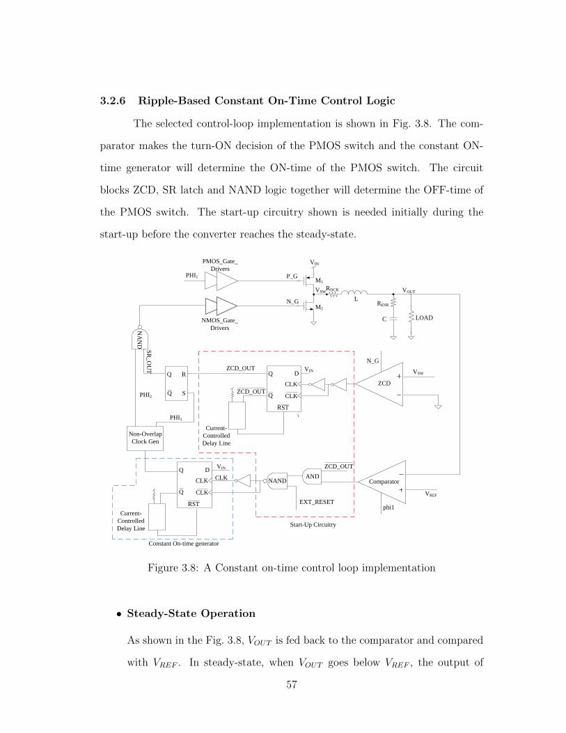
3.2.6 Ripple-Based Constant On-Time Control Logic
The selected control-loop implementation is shown in Fig. 3.8. The com-
parator makes the turn-ON decision of the PMOS switch and the constant ON-
time generator will determine the ON-time of the PMOS switch. The circuit
blocks ZCD, SR latch and NAND logic together will determine the OFF-time of
the PMOS switch. The start-up circuitry shown is needed initially during the
start-up before the converter reaches the steady-state.
VREF
ANDNAND
EXT_RESET
PMOS_Gate_
Drivers
NMOS_Gate_
Drivers
Current-
Controlled
Delay Line
CLK
L
C
VIN
M1
M2
RDCR
RESR
VOUTVSW
LOAD
P_G
N_G
phi1
VIN
RQ
SQ
NA
ND
VSWD
CLK
CLK
RST
Q
Q
D
CLK
CLK
RST
Q
Q
Non-Overlap
Clock Gen
VIN
Current-
Controlled
Delay Line
ZCD_OUT
ZCD_OUT
ZCD_OUT
N_G
Start-Up Circuitry
mComparator
mZCD
PHI2
Constant On-time generator
SR
_O
UT
PHI1
PHI1
Figure 3.8: A Constant on-time control loop implementation
• Steady-State Operation
As shown in the Fig. 3.8, VOUT is fed back to the comparator and compared
with VREF . In steady-state, when VOUT goes below VREF , the output of
57
the comparator goes high. The signal ZCD OUT is always high and goes
low only at the end of phase 2, whereas the signal EXT RESET is always
high during the steady-state. The comparator output along with the start-
up circuitry will generate the clock for the D flip-flop. As the comparator
output is high, the clock of the positive-edge triggered flip-flop also goes
high, which generates a constant on-time signal at the output of the flip-
flop Q. Q is further fed as an input to the non-overlapping clock generator to
generate two output signals, phi1 and phi2 with a short dead-time in between
them. Signals phi1 and phi2 are complementary to each other. phi1, which
contains the constant on-time information, is fed as an input to the PMOS
gate driver. The inverted phi1 signal at the output of the PMOS gate driver
turns ON the PMOS switch for a fixed time, i.e., for a constant on-time.
In the steady-state, whenever the comparator output goes high, a positive
clock edge occurs at D flip-flop.
At the positive clock-edge of the D flip-flop, Q goes high and Q goes low.
Q is delayed through a current-starved delay line and the delayed signal is
fed to the asynchronous low reset of the flip-flop. So, after a predetermined
delay set by the current-starved delay line, the flip-flop is reset, which will
make Q go low. Therefore, Q stays high for a fixed time and then goes low,
which makes it a constant on-time signal. Whenever a positive clock-edge
occurs, a constant pulse width signal is generated at Q.
The ZCD, SR latch and NAND gate ensures that the NMOS switch remains
turned OFF while the PMOS switch is turned ON. The signals SR OUT and
phi2, which are inputs to the NAND gate, determine the turn-ON and turn-
OFF events of the NMOS switch. phi1, which is the input to PMOS gate
driver, is also fed to the SET input of the SR latch, whereas, ZCD OUT
58
is fed to the RESET input. When the PMOS switch is turned ON, phi1 is
high and ZCD OUT is low, which sets the SR latch and makes SR OUT
high. When phi1 is high, phi2 is low. With SR OUT high and phi2 low,
the output of the NAND gate is high. The signal at the NAND gate output
is inverted at the output of the NMOS gate drivers, which turns OFF the
NMOS switch.
When phi1 goes low after a constant on-time, the PMOS switch is turned
OFF. SR OUT , which was already high, latches in the previous output
state and remains high. After phi1 goes low, phi2 goes high after a short
dead-time. As both phi2 and SR OUT are high, the output of the NAND
gate goes low, which gets inverted at the output of the NMOS gate driver
to turn ON the NMOS switch. Therefore, the NMOS is turned-ON after a
short dead-time after the PMOS turn-OFF.
After the turn-ON of the NMOS switch, the inductor current starts decreas-
ing and switching node VSW is at a negative voltage. VSW is fed as an input
to the ZCD, while the other input is ground. The ZCD is enabled only after
the NMOS is turned ON and is disabled when the NMOS turns OFF. When
the ZCD is turned ON, VSW is at a small negative voltage, which gradu-
ally increases towards a positive voltage. As soon as the inductor current
reaches zero, VSW reaches zero volts. When VSW crosses zero, the output of
the ZCD goes high and resets the SR latch. This makes the output of the
NAND gate high and turns OFF the NMOS switch.
After the NMOS switch is turned OFF, both switches remain OFF and
during this period, the output capacitor discharges to supply power to the
load. During this period, the slope of VOUT , i.e., the discharge rate of the
59
output capacitor, is determined by the RC time constant of the output
capacitor (C) and the load resistance (R). The PMOS switch is again turned
ON when VOUT goes below VREF . If the discharge rate is slow, the time for
VOUT to go below VREF increases and the PMOS turn-ON is delayed. This
translates into an increased switching period (TSW ) and decreased switching
frequency (fSW ).
The steady-state DC-DC converter operation in one complete switching cy-
cle is explained in the above discussion. When VOUT again goes below VREF ,
comparator output goes high and a new switching cycle starts. The fre-
quency at which this cycle repeats is the switching frequency (fSW ).
• Start-Up Operation
If only for the steady-state operation, the comparator output can be directly
fed as a clock to the D flip-flop. However, directly feeding the comparator
output to the D flip-flop will never allow the converter to start-up. This
start-up issue and the solution to this issue are discussed below.
It is important to observe that it is the positive clock-edge to the D flip-
flop that generates the constant on-time for the PMOS switch and starts a
new switching cycle every time. In the steady-state, the comparator output
goes high when VOUT goes below VREF and the comparator output goes low
when VOUT goes above VREF . If the comparator output is directly fed to
the D flip-flop clock input, the positive clock-edge to the D flip-flop in every
switching cycle can be provided by the comparator when VOUT goes below
VREF .
However, at start-up, when VOUT is far below VREF , the comparator output
goes high once initially and will never switch to low until VOUT goes above
60
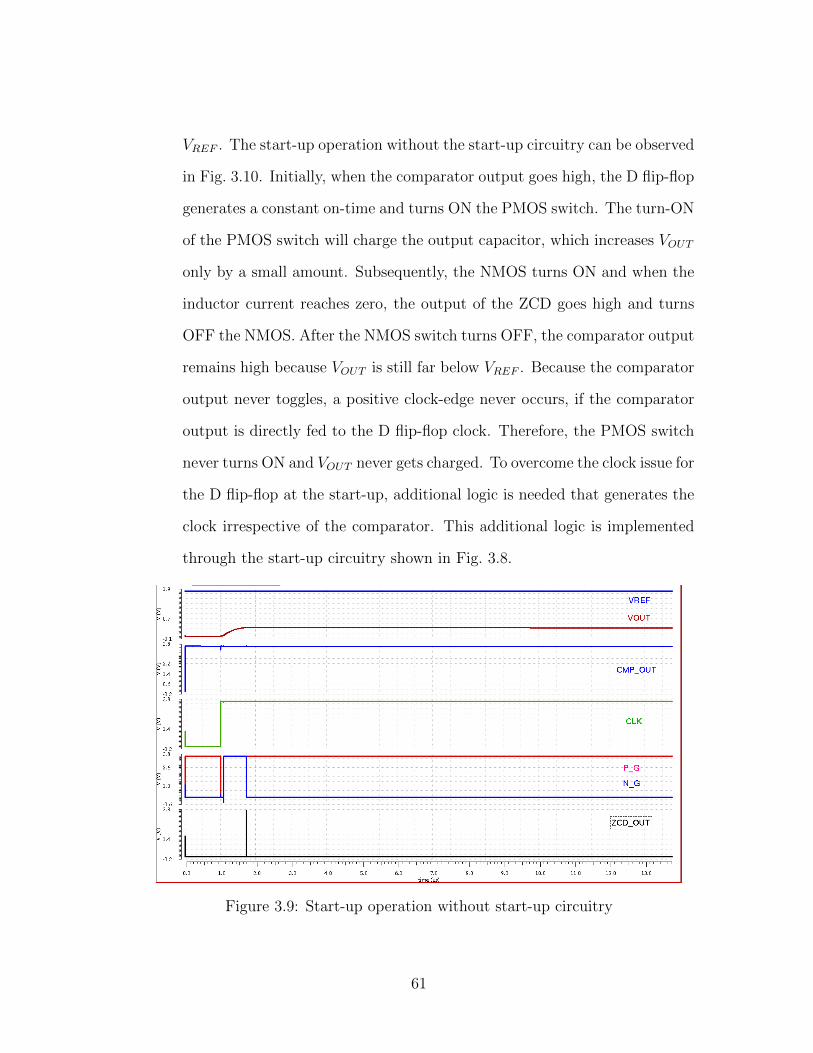
VREF . The start-up operation without the start-up circuitry can be observed
in Fig. 3.10. Initially, when the comparator output goes high, the D flip-flop
generates a constant on-time and turns ON the PMOS switch. The turn-ON
of the PMOS switch will charge the output capacitor, which increases VOUT
only by a small amount. Subsequently, the NMOS turns ON and when the
inductor current reaches zero, the output of the ZCD goes high and turns
OFF the NMOS. After the NMOS switch turns OFF, the comparator output
remains high because VOUT is still far below VREF . Because the comparator
output never toggles, a positive clock-edge never occurs, if the comparator
output is directly fed to the D flip-flop clock. Therefore, the PMOS switch
never turns ON and VOUT never gets charged. To overcome the clock issue for
the D flip-flop at the start-up, additional logic is needed that generates the
clock irrespective of the comparator. This additional logic is implemented
through the start-up circuitry shown in Fig. 3.8.
Figure 3.9: Start-up operation without start-up circuitry
61
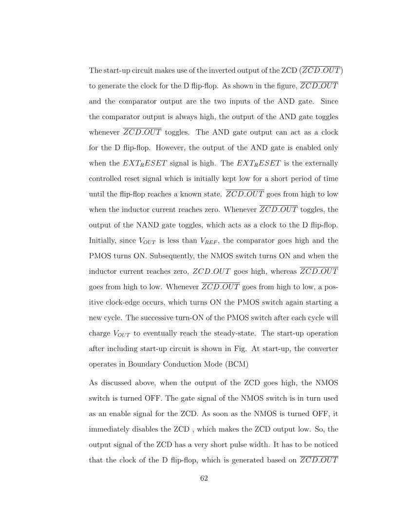
The start-up circuit makes use of the inverted output of the ZCD (ZCD OUT )
to generate the clock for the D flip-flop. As shown in the figure, ZCD OUT
and the comparator output are the two inputs of the AND gate. Since
the comparator output is always high, the output of the AND gate toggles
whenever ZCD OUT toggles. The AND gate output can act as a clock
for the D flip-flop. However, the output of the AND gate is enabled only
when the EXTRESET signal is high. The EXTRESET is the externally
controlled reset signal which is initially kept low for a short period of time
until the flip-flop reaches a known state. ZCD OUT goes from high to low
when the inductor current reaches zero. Whenever ZCD OUT toggles, the
output of the NAND gate toggles, which acts as a clock to the D flip-flop.
Initially, since VOUT is less than VREF , the comparator goes high and the
PMOS turns ON. Subsequently, the NMOS switch turns ON and when the
inductor current reaches zero, ZCD OUT goes high, whereas ZCD OUT
goes from high to low. Whenever ZCD OUT goes from high to low, a pos-
itive clock-edge occurs, which turns ON the PMOS switch again starting a
new cycle. The successive turn-ON of the PMOS switch after each cycle will
charge VOUT to eventually reach the steady-state. The start-up operation
after including start-up circuit is shown in Fig. At start-up, the converter
operates in Boundary Conduction Mode (BCM)
As discussed above, when the output of the ZCD goes high, the NMOS
switch is turned OFF. The gate signal of the NMOS switch is in turn used
as an enable signal for the ZCD. As soon as the NMOS is turned OFF, it
immediately disables the ZCD , which makes the ZCD output low. So, the
output signal of the ZCD has a very short pulse width. It has to be noticed
that the clock of the D flip-flop, which is generated based on ZCD OUT
62
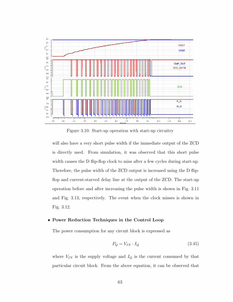
Figure 3.10: Start-up operation with start-up circuitry
will also have a very short pulse width if the immediate output of the ZCD
is directly used. From simulation, it was observed that this short pulse
width causes the D flip-flop clock to miss after a few cycles during start-up.
Therefore, the pulse width of the ZCD output is increased using the D flip-
flop and current-starved delay line at the output of the ZCD. The start-up
operation before and after increasing the pulse width is shown in Fig. 3.11
and Fig. 3.13, respectively. The event when the clock misses is shown in
Fig. 3.12.
• Power Reduction Techniques in the Control Loop
The power consumption for any circuit block is expressed as
PQ = VIN · IQ (3.45)
where VIN is the supply voltage and IQ is the current consumed by that
particular circuit block. From the above equation, it can be observed that
63
Figure 3.11: Start-up when the clock misses
Figure 3.12: D flip-flop clock misses as RST is low when the clock edge occurs
the power consumption in the circuit is directly proportional to the current
consumed by that circuit.
Power consumption in the controller, which is not significant at high loads,
will dominate at light and ultra-light loads. Therefore, it is essential to
64
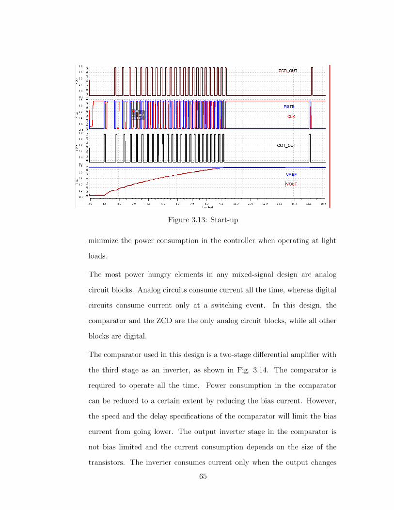
Figure 3.13: Start-up
minimize the power consumption in the controller when operating at light
loads.
The most power hungry elements in any mixed-signal design are analog
circuit blocks. Analog circuits consume current all the time, whereas digital
circuits consume current only at a switching event. In this design, the
comparator and the ZCD are the only analog circuit blocks, while all other
blocks are digital.
The comparator used in this design is a two-stage differential amplifier with
the third stage as an inverter, as shown in Fig. 3.14. The comparator is
required to operate all the time. Power consumption in the comparator
can be reduced to a certain extent by reducing the bias current. However,
the speed and the delay specifications of the comparator will limit the bias
current from going lower. The output inverter stage in the comparator is
not bias limited and the current consumption depends on the size of the
transistors. The inverter consumes current only when the output changes
65
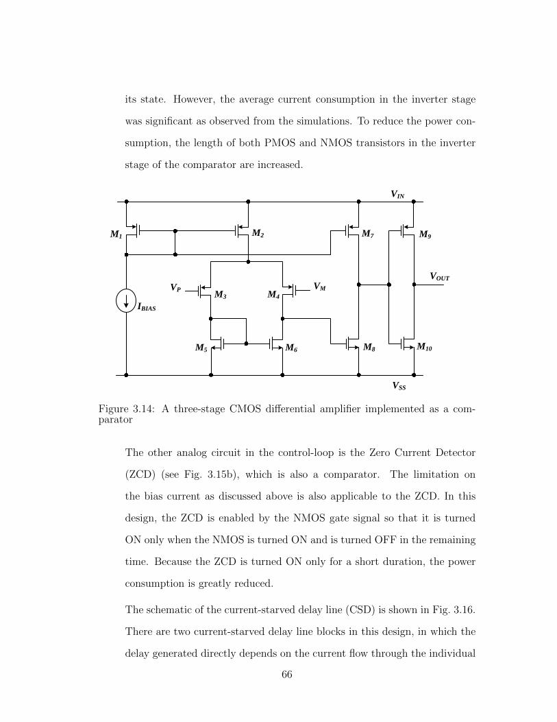
its state. However, the average current consumption in the inverter stage
was significant as observed from the simulations. To reduce the power con-
sumption, the length of both PMOS and NMOS transistors in the inverter
stage of the comparator are increased.
VIN
VSS
VP VM
M1 M2
M3 M4
M5 M6
M7
M8
M9
M10
VOUT
IBIAS
Figure 3.14: A three-stage CMOS differential amplifier implemented as a com-parator
The other analog circuit in the control-loop is the Zero Current Detector
(ZCD) (see Fig. 3.15b), which is also a comparator. The limitation on
the bias current as discussed above is also applicable to the ZCD. In this
design, the ZCD is enabled by the NMOS gate signal so that it is turned
ON only when the NMOS is turned ON and is turned OFF in the remaining
time. Because the ZCD is turned ON only for a short duration, the power
consumption is greatly reduced.
The schematic of the current-starved delay line (CSD) is shown in Fig. 3.16.
There are two current-starved delay line blocks in this design, in which the
delay generated directly depends on the current flow through the individual
66
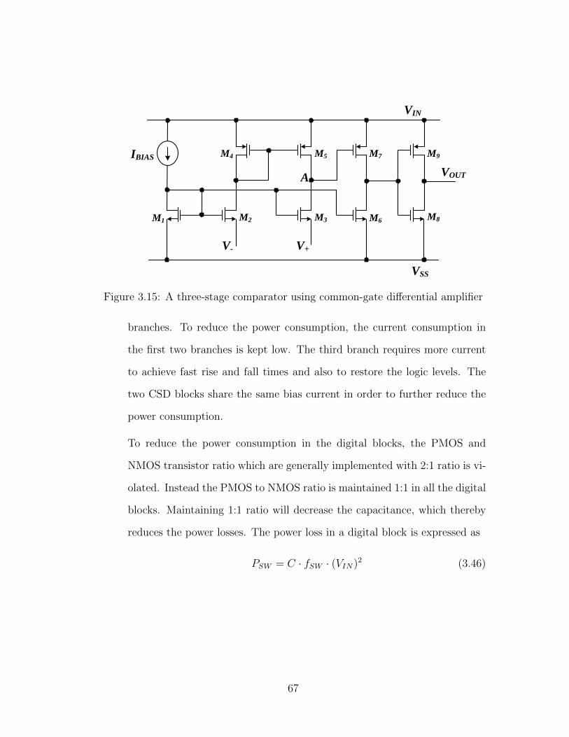
M1
M4IBIAS
VIN
M2 M3
M5
V+
M6
M7
M8
M9
VSS
VOUTA
V-
Figure 3.15: A three-stage comparator using common-gate differential amplifier
branches. To reduce the power consumption, the current consumption in
the first two branches is kept low. The third branch requires more current
to achieve fast rise and fall times and also to restore the logic levels. The
two CSD blocks share the same bias current in order to further reduce the
power consumption.
To reduce the power consumption in the digital blocks, the PMOS and
NMOS transistor ratio which are generally implemented with 2:1 ratio is vi-
olated. Instead the PMOS to NMOS ratio is maintained 1:1 in all the digital
blocks. Maintaining 1:1 ratio will decrease the capacitance, which thereby
reduces the power losses. The power loss in a digital block is expressed as
PSW = C · fSW · (VIN)2 (3.46)
67
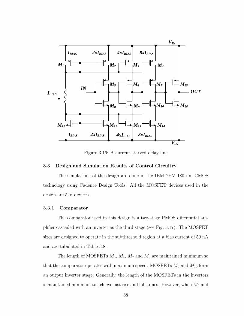
VIN
VSS
OUTIBIAS
M1 M2 M3 M4
M11 M12 M13 M14
INM5
M8
M6
M9
M7
M10
M15
M16
2xIBIAS 4xIBIASIBIAS 8xIBIAS
IBIAS 2xIBIAS 4xIBIAS 8xIBIAS
Figure 3.16: A current-starved delay line
3.3 Design and Simulation Results of Control Circuitry
The simulations of the design are done in the IBM 7HV 180 nm CMOS
technology using Cadence Design Tools. All the MOSFET devices used in the
design are 5-V devices.
3.3.1 Comparator
The comparator used in this design is a two-stage PMOS differential am-
plifier cascaded with an inverter as the third stage (see Fig. 3.17). The MOSFET
sizes are designed to operate in the subthreshold region at a bias current of 50 nA
and are tabulated in Table 3.8.
The length of MOSFETs M3, M4, M7 and M8 are maintained minimum so
that the comparator operates with maximum speed. MOSFETs M9 and M10 form
an output inverter stage. Generally, the length of the MOSFETs in the inverters
is maintained minimum to achieve fast rise and fall-times. However, when M9 and
68
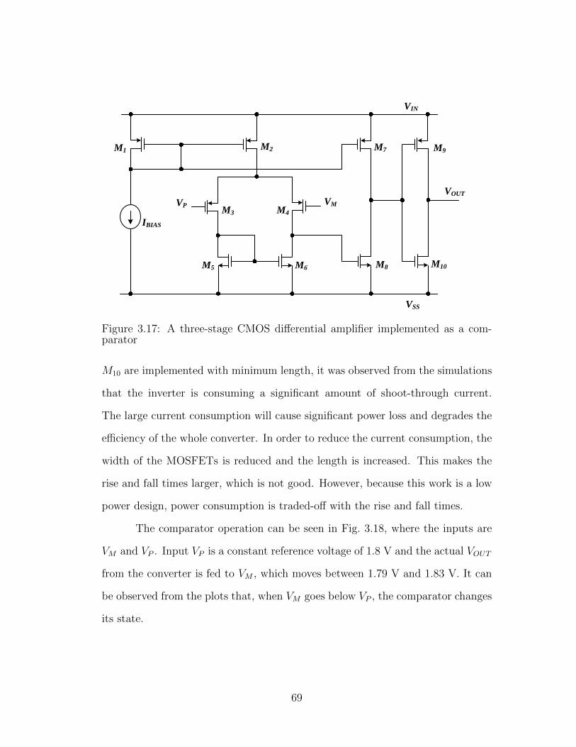
VIN
VSS
VP VM
M1 M2
M3 M4
M5 M6
M7
M8
M9
M10
VOUT
IBIAS
Figure 3.17: A three-stage CMOS differential amplifier implemented as a com-parator
M10 are implemented with minimum length, it was observed from the simulations
that the inverter is consuming a significant amount of shoot-through current.
The large current consumption will cause significant power loss and degrades the
efficiency of the whole converter. In order to reduce the current consumption, the
width of the MOSFETs is reduced and the length is increased. This makes the
rise and fall times larger, which is not good. However, because this work is a low
power design, power consumption is traded-off with the rise and fall times.
The comparator operation can be seen in Fig. 3.18, where the inputs are
VM and VP . Input VP is a constant reference voltage of 1.8 V and the actual VOUT
from the converter is fed to VM , which moves between 1.79 V and 1.83 V. It can
be observed from the plots that, when VM goes below VP , the comparator changes
its state.
69
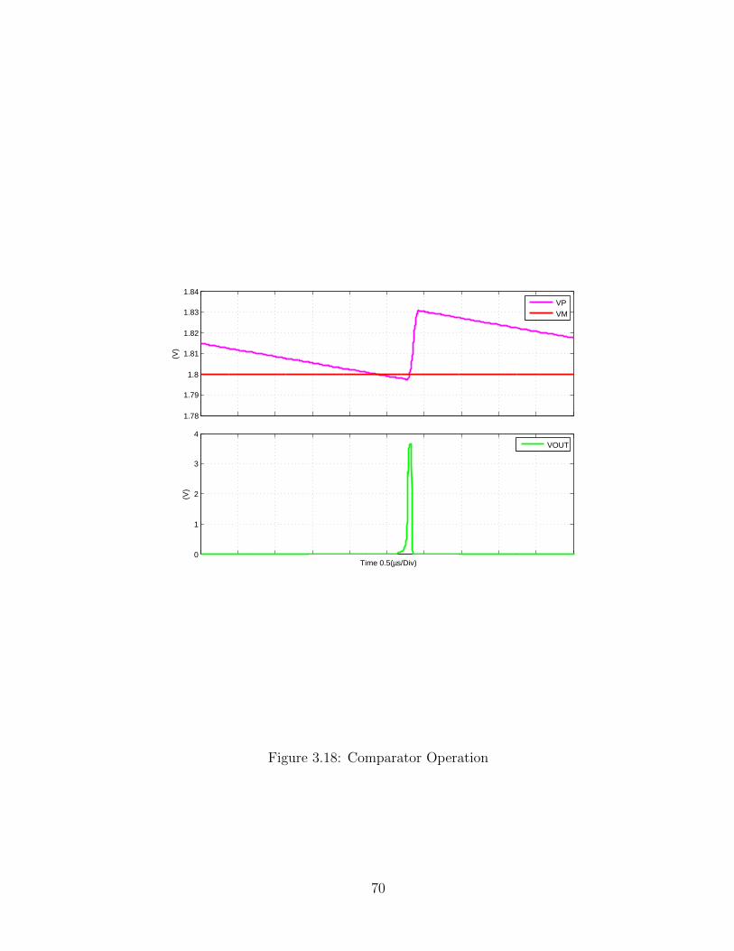
1.78
1.79
1.8
1.81
1.82
1.83
1.84
(V)
VPVM
0
1
2
3
4
(V)
Time 0.5(µs/Div)
VOUT
Figure 3.18: Comparator Operation
70
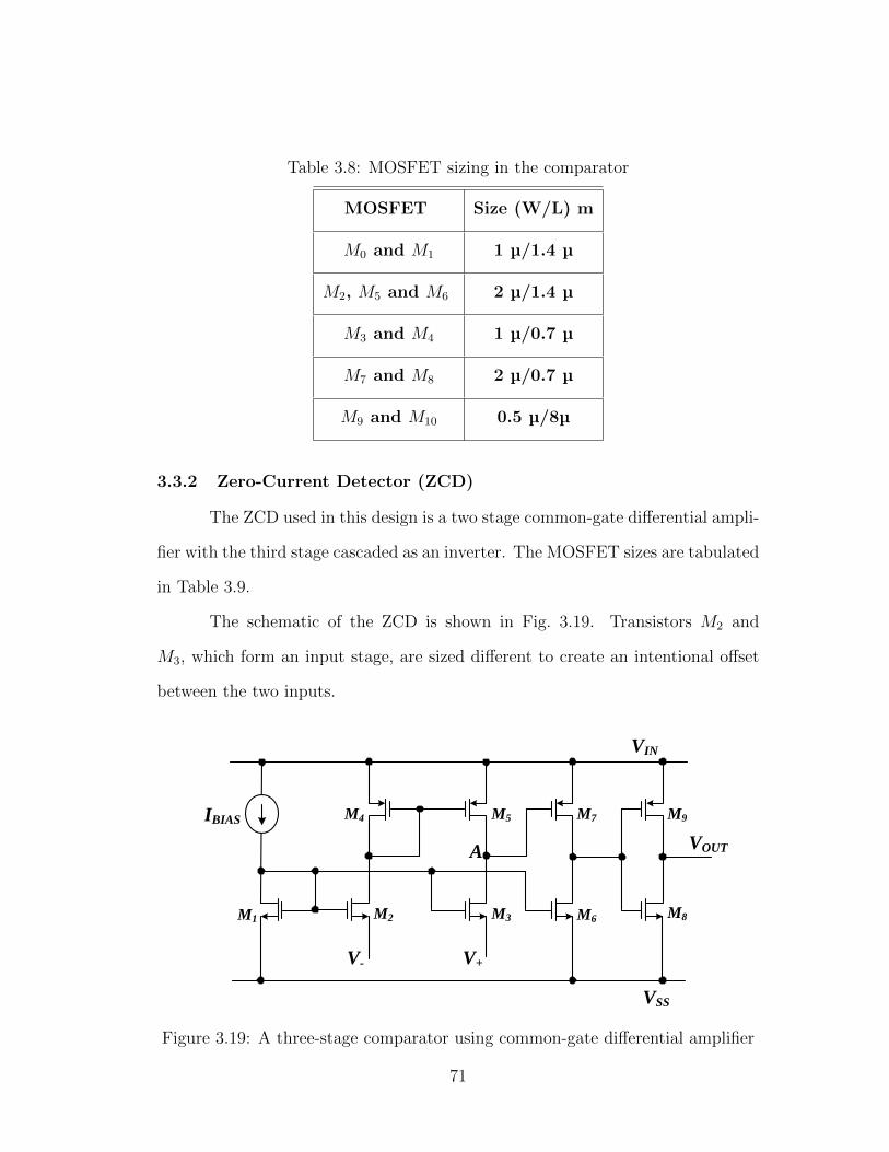
Table 3.8: MOSFET sizing in the comparator
MOSFET Size (W/L) m
M0 and M1 1 µ/1.4 µ
M2, M5 and M6 2 µ/1.4 µ
M3 and M4 1 µ/0.7 µ
M7 and M8 2 µ/0.7 µ
M9 and M10 0.5 µ/8µ
3.3.2 Zero-Current Detector (ZCD)
The ZCD used in this design is a two stage common-gate differential ampli-
fier with the third stage cascaded as an inverter. The MOSFET sizes are tabulated
in Table 3.9.
The schematic of the ZCD is shown in Fig. 3.19. Transistors M2 and
M3, which form an input stage, are sized different to create an intentional offset
between the two inputs.
M1
M4IBIAS
VIN
M2 M3
M5
V+
M6
M7
M8
M9
VSS
VOUTA
V-
Figure 3.19: A three-stage comparator using common-gate differential amplifier
71

The working of the ZCD is shown in the Fig. 3.20. The negative input VM
is connected to the ground, whereas the actual switching node VSW is fed to the
positive input VP . From the figure, it can be observed that whenever VSW crosses
ground, ZCDOUT changes its state.
Table 3.9: MOSFET sizing in the ZCD
MOSFET Size (W/L) m
M1 1.4 µ/1.4 µ
M2 22.4 µ/1.4 µ
M3, M4 and M5 5.6 µ/1.4 µ
M6 2.8 µ/0.7 µ
M7 1.4 µ/0.7µ
M8 and M9 0.5 µ/0.7µ
3.3.3 Non-Overlapping Clock Generator (NOCG)
The NOCG is implemented using an SR-latch with NAND gates. The
topology is shown in Fig. 3.21.
All the resistors used in NOCG have the same value, which is equal to
1.2 kΩ. The sizes of the inverters are tabulated in Table 3.10. Signals phi1 and
phi2 and the dead-time generated between them is shown in Fig. 3.22. The dead-
time on both sides is the same and is equal to 4 ns. Signals phi1 and phi2 are
complementary to each other.
3.3.4 Current-Starved Delay-Line (CSD)
The schematic of the CSD is shown in Fig. 3.23 and the MOSFET sizes
are tabulated in Table. 3.11. The bias current is 65 nA.
72

−1
−0.5
0
0.5
1
(V)
VSWVSS
0
1
2
3
4
(V)
Time 0.05(µs)/Div
ZCD_OUT
Figure 3.20: Inputs and output signals of ZCD
There are three inverter stages in series, which are current limited by the
top and bottom transistors. The operation of the CSD is described in Sec. 2.6.5.
73
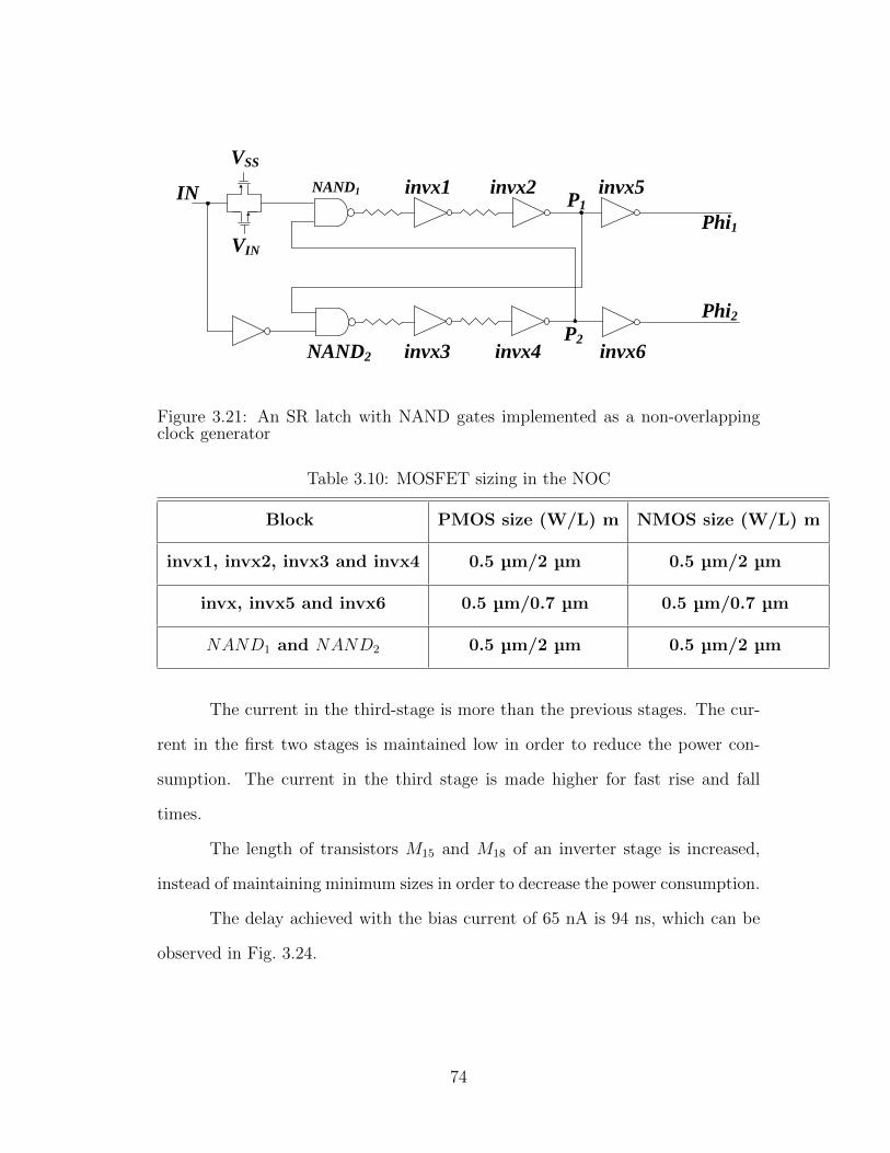
IN
VIN
VSS
Phi1
Phi2
P1
P2
NAND1
NAND2
invx1 invx2
invx3 invx4
invx5
invx6
Figure 3.21: An SR latch with NAND gates implemented as a non-overlappingclock generator
Table 3.10: MOSFET sizing in the NOC
Block PMOS size (W/L) m NMOS size (W/L) m
invx1, invx2, invx3 and invx4 0.5 µm/2 µm 0.5 µm/2 µm
invx, invx5 and invx6 0.5 µm/0.7 µm 0.5 µm/0.7 µm
NAND1 and NAND2 0.5 µm/2 µm 0.5 µm/2 µm
The current in the third-stage is more than the previous stages. The cur-
rent in the first two stages is maintained low in order to reduce the power con-
sumption. The current in the third stage is made higher for fast rise and fall
times.
The length of transistors M15 and M18 of an inverter stage is increased,
instead of maintaining minimum sizes in order to decrease the power consumption.
The delay achieved with the bias current of 65 nA is 94 ns, which can be
observed in Fig. 3.24.
74
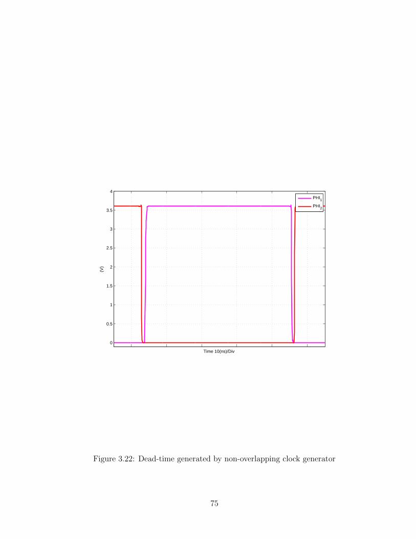
0
0.5
1
1.5
2
2.5
3
3.5
4
(V)
Time 10(ns)/Div
PHI1PHI2
Figure 3.22: Dead-time generated by non-overlapping clock generator
75
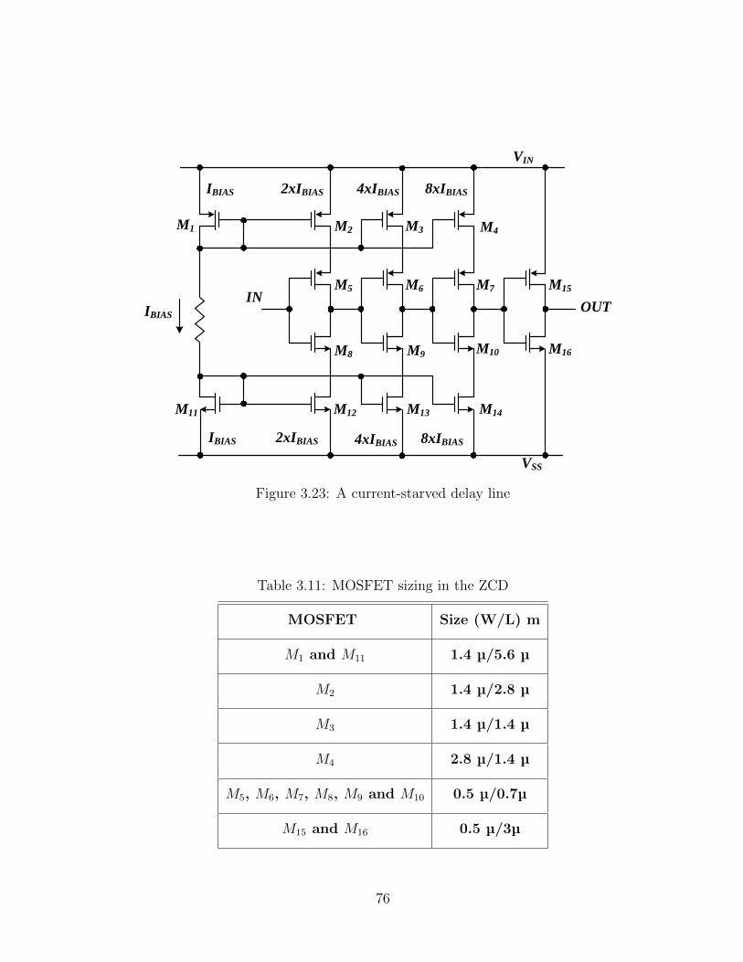
VIN
VSS
OUTIBIAS
M1 M2 M3 M4
M11 M12 M13 M14
INM5
M8
M6
M9
M7
M10
M15
M16
2xIBIAS 4xIBIASIBIAS 8xIBIAS
IBIAS 2xIBIAS 4xIBIAS 8xIBIAS
Figure 3.23: A current-starved delay line
Table 3.11: MOSFET sizing in the ZCD
MOSFET Size (W/L) m
M1 and M11 1.4 µ/5.6 µ
M2 1.4 µ/2.8 µ
M3 1.4 µ/1.4 µ
M4 2.8 µ/1.4 µ
M5, M6, M7, M8, M9 and M10 0.5 µ/0.7µ
M15 and M16 0.5 µ/3µ
76
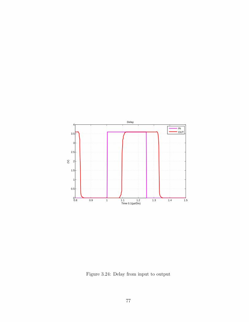
0.8 0.9 1 1.1 1.2 1.3 1.4 1.50
0.5
1
1.5
2
2.5
3
3.5
4
(V)
Time 0.1(µs/Div)
Delay
INOUT
Figure 3.24: Delay from input to output
77
Chapter 4
SYSTEM-LEVEL SIMULATIONS OF BUCK CONVERTER
This chapter discusses the simulation results of the converter and control-loop.
Simulations across a wide load current range are discussed here.
4.1 Simulation Results at Minimum Load
The converter is optimized at 20 µA load current which is also the minimum
load of this design. The test bench for the system level converter is shown in
Fig. 4.1. The simulated waveforms of the output voltage and the clock signals
are shown in Fig. 4.2. The inductor current, output current and switching node
waveforms can be observed in Fig. 4.3
The steady-state waveforms are shown in Figs. 4.4 and 4.5. In steady-state,
〈VOUT 〉 settles to 1.814 V and the the output voltage ripple (∆VOUT ) is 33.36 mV.
The constant on-time of the PMOS switch is 94.5 ns. The switching fre-
quency is 184.8 kHz. The total time of operation is 156 ns, whereas, the switching
period is 5.41 µs. Therefore, it can be said that the converter operates in deep
DCM. Results from the simulations are summarized in Table 4.1.
The role of the ZCD in the converter can be observed in Fig. 4.6. As soon
as VSW reaches zero, ZCD OUT goes high, which turns OFF the NMOS switch.
It can also be observed from the same figure that the inductor current also reaches
zero when VSW reaches zero.
The efficiency of the converter can be calculated from
η ≡ POUT
PIN
(4.1)
78
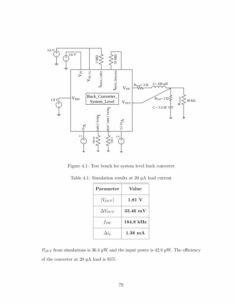
L= 100 µHRDCR= 3 Ω
RESR= 2 Ω
C = 3.3 nF
90 kΩ
3.6 V
+-
1.8 V
VIN
VIN
_C
L
I BIA
S_
CM
P2
I BIA
S_
Del
ayli
ne
VREF
VSW
VOUT
VS
S
VS
S_
CL
IB
IAS
_C
MP
1
IB
IAS
_C
MP
1_
AD
D
5 MΩ
35 MΩ
60
MΩ
2 MΩ
+- +
-
+-
+-
0 V 0 V
3.6 V
RL
OA
DBuck_Converter_
System_Level
Figure 4.1: Test bench for system level buck converter
Table 4.1: Simulation results at 20 µA load current
Parameter Value
〈VOUT 〉 1.81 V
∆VOUT 33.46 mV
fSW 184.8 kHz
∆iL 1.38 mA
POUT from simulations is 36.4 µW and the input power is 42.8 µW. The efficiency
of the converter at 20 µA load is 85%.
79
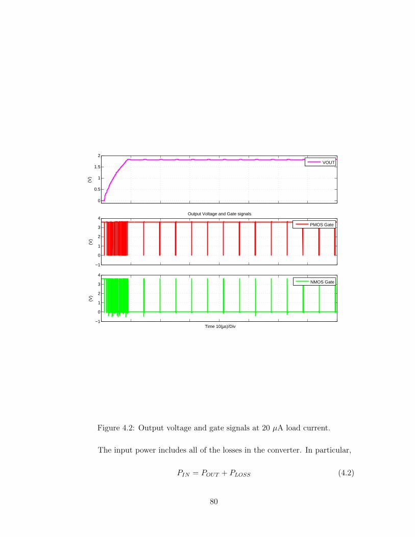
0
0.5
1
1.5
2
(V)
VOUT
−1
0
1
2
3
4
(V)
Output Voltage and Gate signals
PMOS Gate
−1
0
1
2
3
4
(V)
Time 10(µs)/Div
NMOS Gate
Figure 4.2: Output voltage and gate signals at 20 µA load current.
The input power includes all of the losses in the converter. In particular,
PIN = POUT + PLOSS (4.2)
80
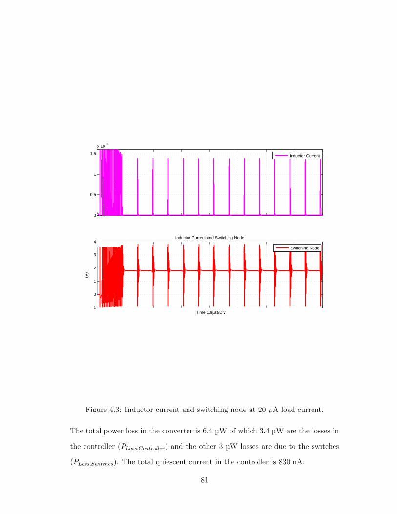
0
0.5
1
1.5
x 10−3
Inductor Current
−1
0
1
2
3
4
(V)
Time 10(µs)/Div
Inductor Current and Switching Node
Switching Node
Figure 4.3: Inductor current and switching node at 20 µA load current.
The total power loss in the converter is 6.4 µW of which 3.4 µW are the losses in
the controller (PLoss,Controller) and the other 3 µW losses are due to the switches
(PLoss,Switches). The total quiescent current in the controller is 830 nA.
81
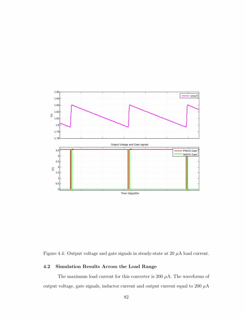
1.78
1.79
1.8
1.81
1.82
1.83
1.84
1.85
(V)
VOUT
0
0.5
1
1.5
2
2.5
3
3.5
(V)
Time 10(µs)/Div
Output Voltage and Gate signals
PMOS GateNMOS Gate
Figure 4.4: Output voltage and gate signals in steady-state at 20 µA load current.
4.2 Simulation Results Across the Load Range
The maximum load current for this converter is 200 µA. The waveforms of
output voltage, gate signals, inductor current and output current equal to 200 µA
82
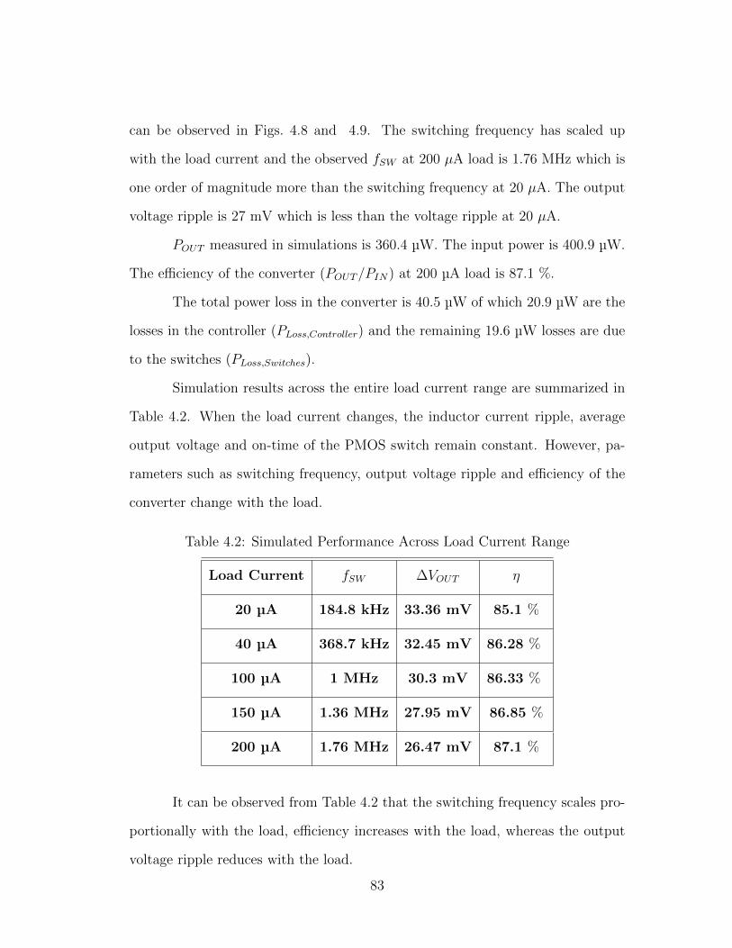
can be observed in Figs. 4.8 and 4.9. The switching frequency has scaled up
with the load current and the observed fSW at 200 µA load is 1.76 MHz which is
one order of magnitude more than the switching frequency at 20 µA. The output
voltage ripple is 27 mV which is less than the voltage ripple at 20 µA.
POUT measured in simulations is 360.4 µW. The input power is 400.9 µW.
The efficiency of the converter (POUT/PIN) at 200 µA load is 87.1 %.
The total power loss in the converter is 40.5 µW of which 20.9 µW are the
losses in the controller (PLoss,Controller) and the remaining 19.6 µW losses are due
to the switches (PLoss,Switches).
Simulation results across the entire load current range are summarized in
Table 4.2. When the load current changes, the inductor current ripple, average
output voltage and on-time of the PMOS switch remain constant. However, pa-
rameters such as switching frequency, output voltage ripple and efficiency of the
converter change with the load.
Table 4.2: Simulated Performance Across Load Current Range
Load Current fSW ∆VOUT η
20 µA 184.8 kHz 33.36 mV 85.1 %
40 µA 368.7 kHz 32.45 mV 86.28 %
100 µA 1 MHz 30.3 mV 86.33 %
150 µA 1.36 MHz 27.95 mV 86.85 %
200 µA 1.76 MHz 26.47 mV 87.1 %
It can be observed from Table 4.2 that the switching frequency scales pro-
portionally with the load, efficiency increases with the load, whereas the output
voltage ripple reduces with the load.
83
4.3 Load Transient Response
The load transient testbench is shown in Fig. 4.10, in which a load re-
sistance of 90 kΩ is fixed and an additional resistance in series with an NMOS
switch is added in parallel to the 90 kΩ resistor. When the switch is OFF, the
load current is 20 µA and when the switch turns ON, additional load current of
180 µA is added to increase the load current from 20 µA to 200 µA. The switch
is controlled by a pulse signal. The rise and fall times of the load current as it
changes between 20 µA and 200 µA are 10 ns.
The output voltage response to the load transient is shown in Fig. 4.11. It
can be observed from the figure that whenever the load current (IOUT ) changes, the
switching frequency of the converter changes. The change in switching frequency
can be observed in the output voltage and gate signal waveforms.
A low to high load transient is shown in Fig. 4.12. From the waveform, it
can be observed that the load current changes from 20 µA to 200 µA. The rise
time is 10 ns. However, the converter does not react to fast changes in the load
current and will not be able to source the increased load current.
As soon as VOUT goes below VREF , the PMOS switch turns ON to charge
VOUT . As discussed previously, the decrease in the load resistance will cause the
switching frequency to increase. Because of the increased switching frequency,
the output capacitor charges more frequently to bring back VOUT to the desired
value. The immediate turn-ON of the PMOS switch when VOUT goes below VREF
prevents undershoot. As such the converter immediately transitions to steady-
state at the higher load current.
The output voltage behavior when a high to low load transient (200 µA
to 20 µA) occurs is shown in Fig. 4.13. When the high-low load transient occurs,
the OFF-time of the converter (i.e., the duration of the converter when both
84

switches are OFF) is increased to bring back VOUT to the desired value. There
is no overshoot in the output voltage. A new steady-state is reached within one
cycle.
How good the converter regulates the average output voltage to a steady-
state changes in load current is known as load regulation. Load regulation is
defined as the ratio of change in the steady-state output voltage to the steady-
state change in load current. Load regulation is expressed as
Looksterrible−−Loadregulation =∆ 〈VOUT 〉∆ 〈IOUT 〉
=VOUT,MAX − VOUT,MIN
IOUT,MAX − IOUT,MIN
(4.3)
For a low-to-high load current change, the steady-state 〈VOUT 〉 at 20 µA is 1.814 V
and the steady-state 〈VOUT 〉 at 200 µA is 1.801 V. The load regulation is
1.814 V − 1.801 V
200 µA− 20 µA= 72 V/A (4.4)
4.4 Line Transient Response
The testbench for line transient is shown in Fig. 4.14, where a pulse signal
is given as an input supply source. The rise and fall times of the pulse signal are
10 ns each. The input varies between 3.0 V and 3.6 V in 10 ns.
The line transient response can be observed in Fig. 4.15.
The line transient response when the input varies from 3.6 V to 3.0 V is
shown in Fig. 4.16
The line transient response when the input varies from 3.0 V to 3.6 V is
shown in Fig. 4.17
Line regulation is defined as the ratio of the steady-state change in output
to the steady-state change in input, which is expressed as
Lineregulation =∆VOUT,STEADY−STATE
∆VIN,STEADY−STATE
=VOUT,MAX − VOUT,MIN
VIN,MAX − VIN,MIN
(4.5)
85
For high to low line transient, i.e., when the input change from 3.6 V to
3.0 V, the steady-state VOUT at 3.6 V is 1.814 V and the steady-state VOUT at
3.0 V is 1.807 V. The line regulation is
1.814 V − 1.807 V
3.6 V − 3.0 V= 11.6 mV /V (4.6)
Similarly, for low to high line transient, i.e., when the input change from
3.0 V to 3.6 V, the steady-state VOUT at 3.6 V is 1.814 V and the steady-state
VOUT at 3.0 V is 1.807 V. The line regulation is
1.814 V − 1.807 V
3.6 V − 3.0 V= 11.6 mV /V (4.7)
86
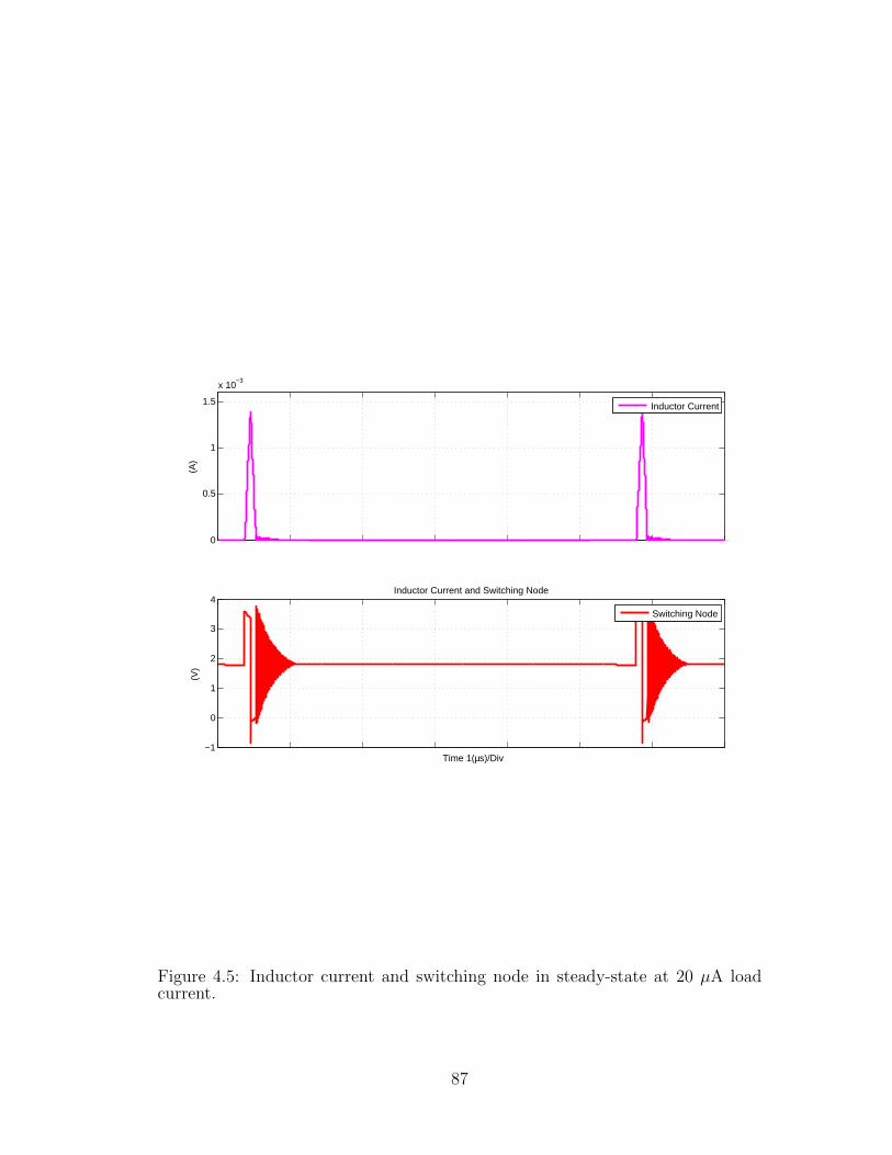
0
0.5
1
1.5
x 10−3
(A)
Inductor Current
−1
0
1
2
3
4
(V)
Time 1(µs)/Div
Inductor Current and Switching Node
Switching Node
Figure 4.5: Inductor current and switching node in steady-state at 20 µA loadcurrent.
87
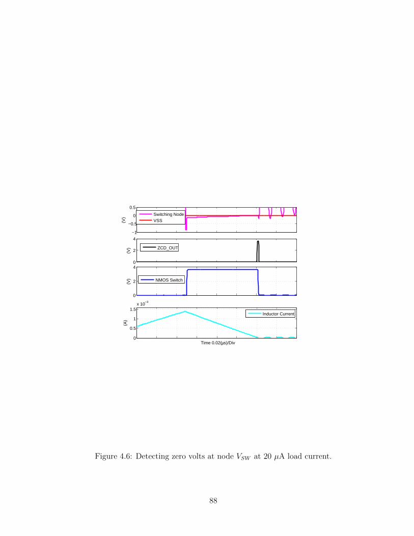
−1
−0.5
0
0.5
(V)
Switching NodeVSS
0
2
4
(V)
ZCD_OUT
0
2
4
(V)
NMOS Switch
0
0.5
1
1.5x 10
−3
(A)
Time 0.02(µs)/Div
Inductor Current
Figure 4.6: Detecting zero volts at node VSW at 20 µA load current.
88
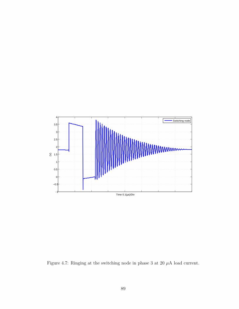
−1
−0.5
0
0.5
1
1.5
2
2.5
3
3.5
4
(V)
Time 0.1(µs)/Div
Switching node
Figure 4.7: Ringing at the switching node in phase 3 at 20 µA load current.
89
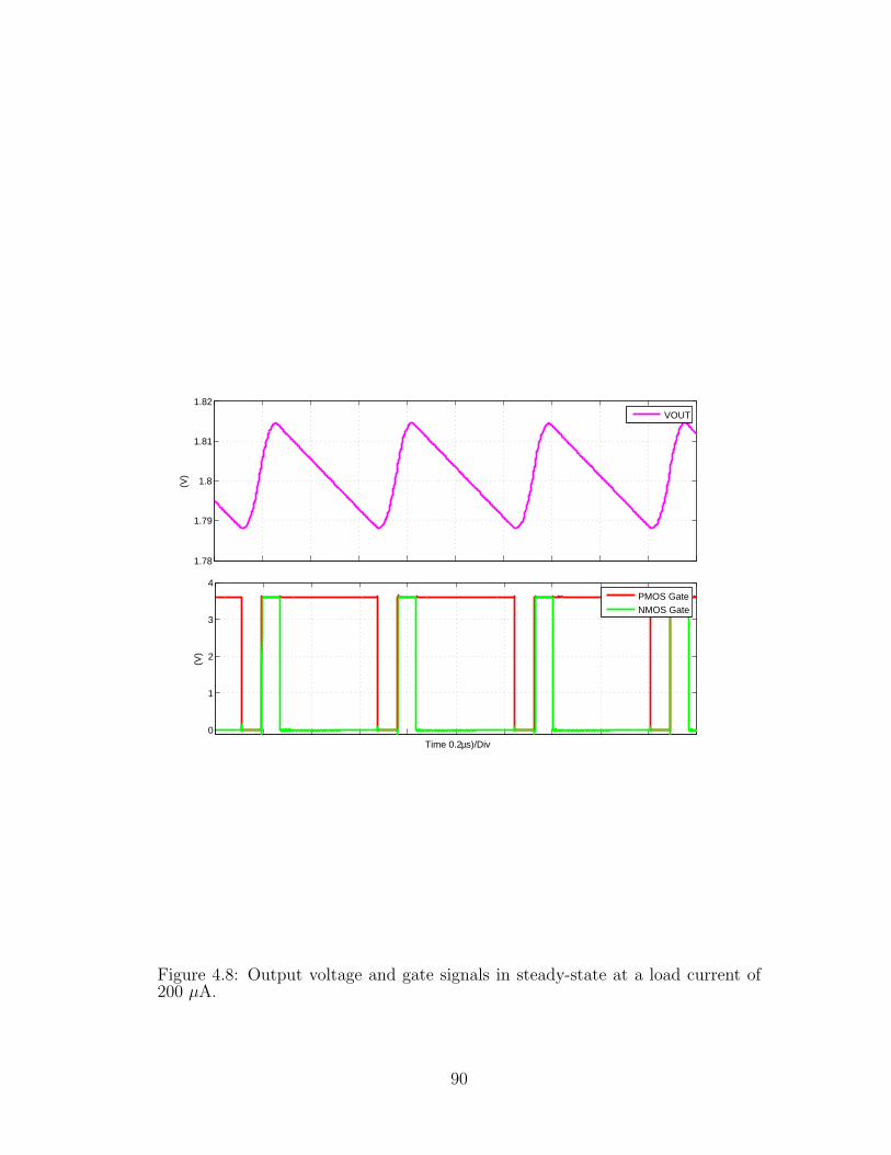
1.78
1.79
1.8
1.81
1.82
(V)
VOUT
0
1
2
3
4
(V)
Time 0.2µs)/Div
PMOS GateNMOS Gate
Figure 4.8: Output voltage and gate signals in steady-state at a load current of200 µA.
90
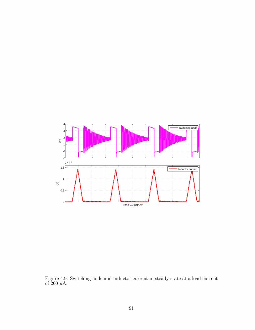
−1
0
1
2
3
4
(V)
Switching node
0
0.5
1
1.5
x 10−3
(A)
Time 0.2(µs)/Div
Inductor current
Figure 4.9: Switching node and inductor current in steady-state at a load currentof 200 µA.
91
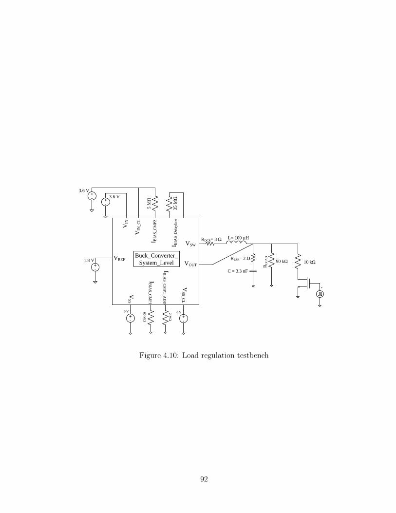
L= 100 µHRDCR= 3 Ω
RESR= 2 Ω
C = 3.3 nF
90 kΩ
3.6 V
+-
1.8 V
VIN
VIN
_C
L
I BIA
S_
CM
P2
I BIA
S_
Del
ayli
ne
VREF
VSW
VOUTV
SS
VS
S_
CL
IB
IAS
_C
MP
1
IB
IAS
_C
MP
1_
AD
D
5 MΩ
35
MΩ
60 MΩ
2 MΩ
+- +
-
+-
+-
0 V 0 V
3.6 V
RL
OA
DBuck_Converter_
System_Level
+
10 kΩ
Figure 4.10: Load regulation testbench
92
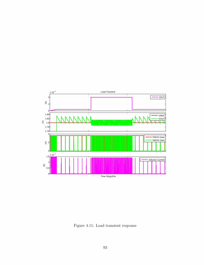
0
1
2
x 10−4
(A)
Load Transient
IOUT
1.76
1.78
1.8
1.82
1.84
(V)
VREFVOUT
0
2
4
(V)
PMOS GateNMOS Gate
0
0.5
1
1.5x 10
−3
(A)
Time 50(µs)/Div
Inductor Current
Figure 4.11: Load transient response
93
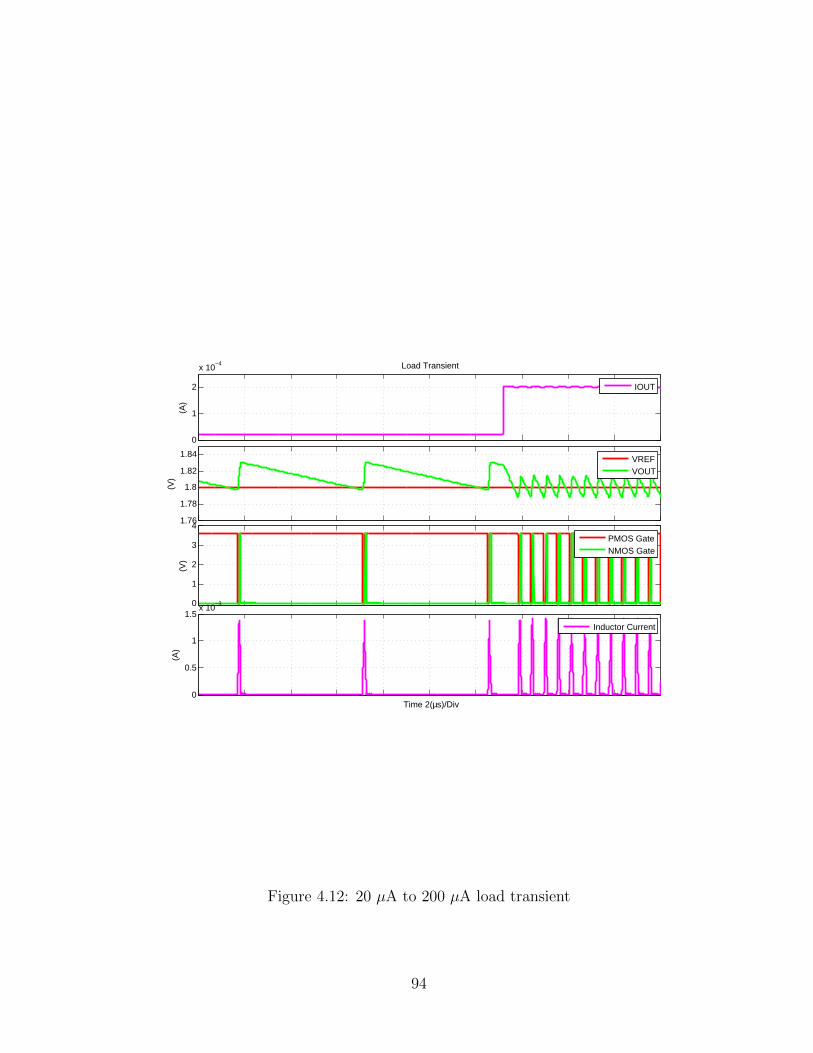
0
1
2
x 10−4
(A)
Load Transient
IOUT
1.76
1.78
1.8
1.82
1.84
(V)
VREFVOUT
0
1
2
3
4
(V)
PMOS GateNMOS Gate
0
0.5
1
1.5x 10
−3
(A)
Time 2(µs)/Div
Inductor Current
Figure 4.12: 20 µA to 200 µA load transient
94
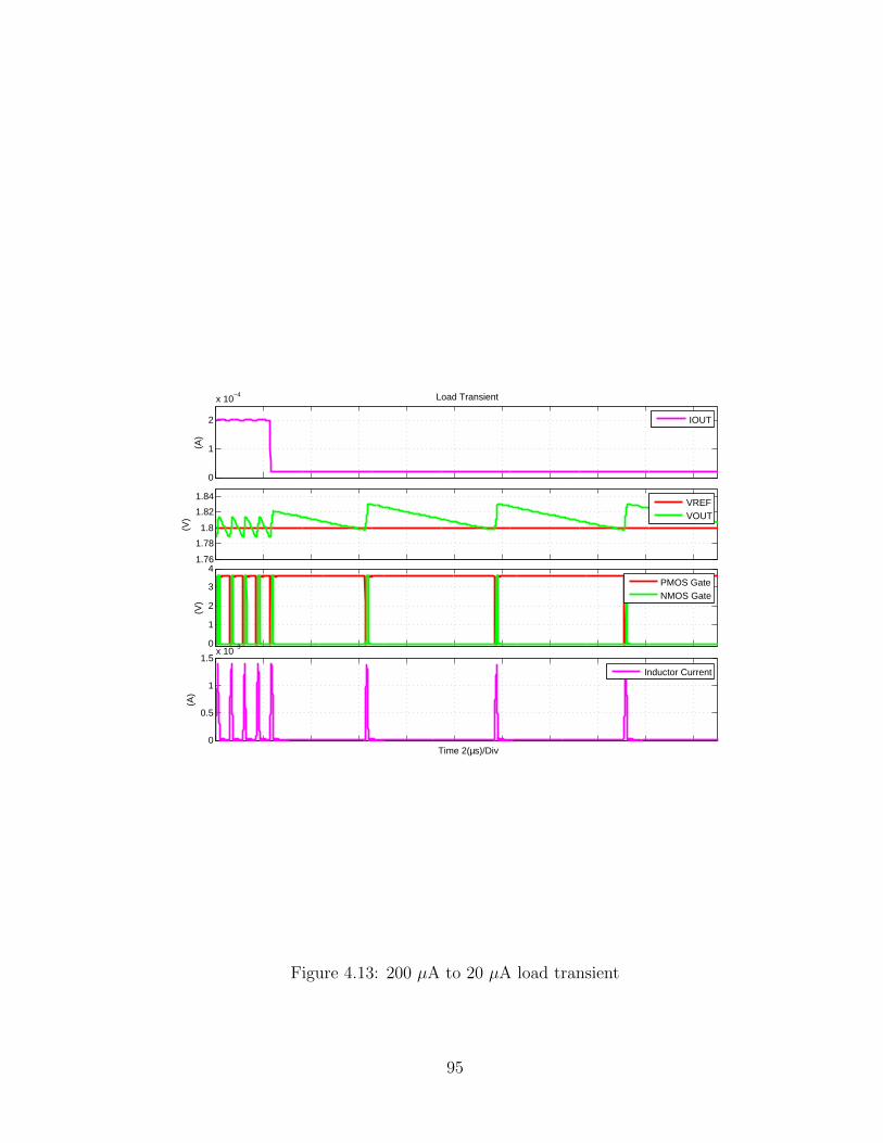
0
1
2
x 10−4
(A)
Load Transient
IOUT
1.76
1.78
1.8
1.82
1.84
(V)
VREFVOUT
0
1
2
3
4
(V)
PMOS GateNMOS Gate
0
0.5
1
1.5x 10
−3
(A)
Time 2(µs)/Div
Inductor Current
Figure 4.13: 200 µA to 20 µA load transient
95
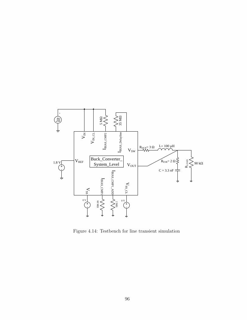
L= 100 µHRDCR= 3 Ω
RESR= 2 Ω
C = 3.3 nF
90 kΩ+-
1.8 V
VIN
VIN
_C
L
I BIA
S_C
MP
2
I BIA
S_
Del
ayli
ne
VREF
VSW
VOUT
VS
S
VS
S_
CL
IB
IAS
_C
MP
1
IB
IAS
_C
MP
1_A
DD
5 MΩ
35 MΩ
60
MΩ
2 MΩ+
-+-
0 V 0 V
RL
OA
DBuck_Converter_
System_Level
+
Figure 4.14: Testbench for line transient simulation
96
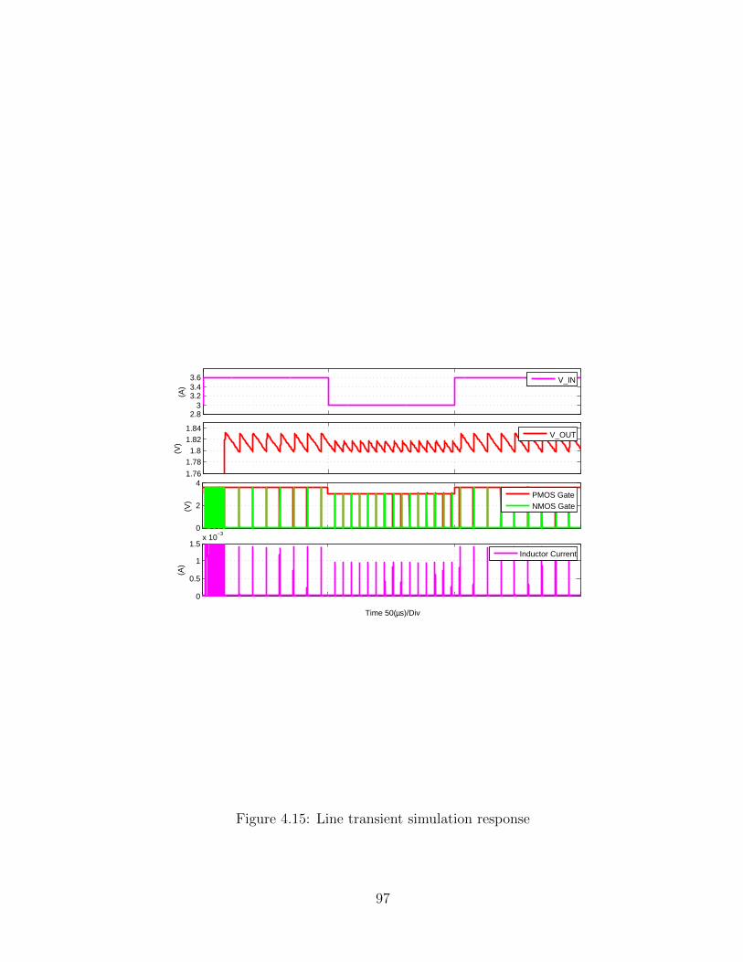
2.83
3.23.43.6
(A)
V_IN
1.76
1.781.8
1.821.84
(V)
V_OUT
0
2
4
(V)
PMOS GateNMOS Gate
0
0.5
1
1.5x 10
−3
(A)
Time 50(µs)/Div
Inductor Current
Figure 4.15: Line transient simulation response
97
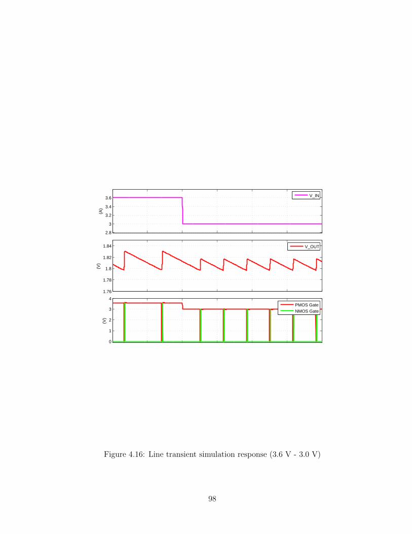
2.8
3
3.2
3.4
3.6
(A)
V_IN
1.76
1.78
1.8
1.82
1.84
(V)
V_OUT
0
1
2
3
4
(V)
PMOS GateNMOS Gate
Figure 4.16: Line transient simulation response (3.6 V - 3.0 V)
98
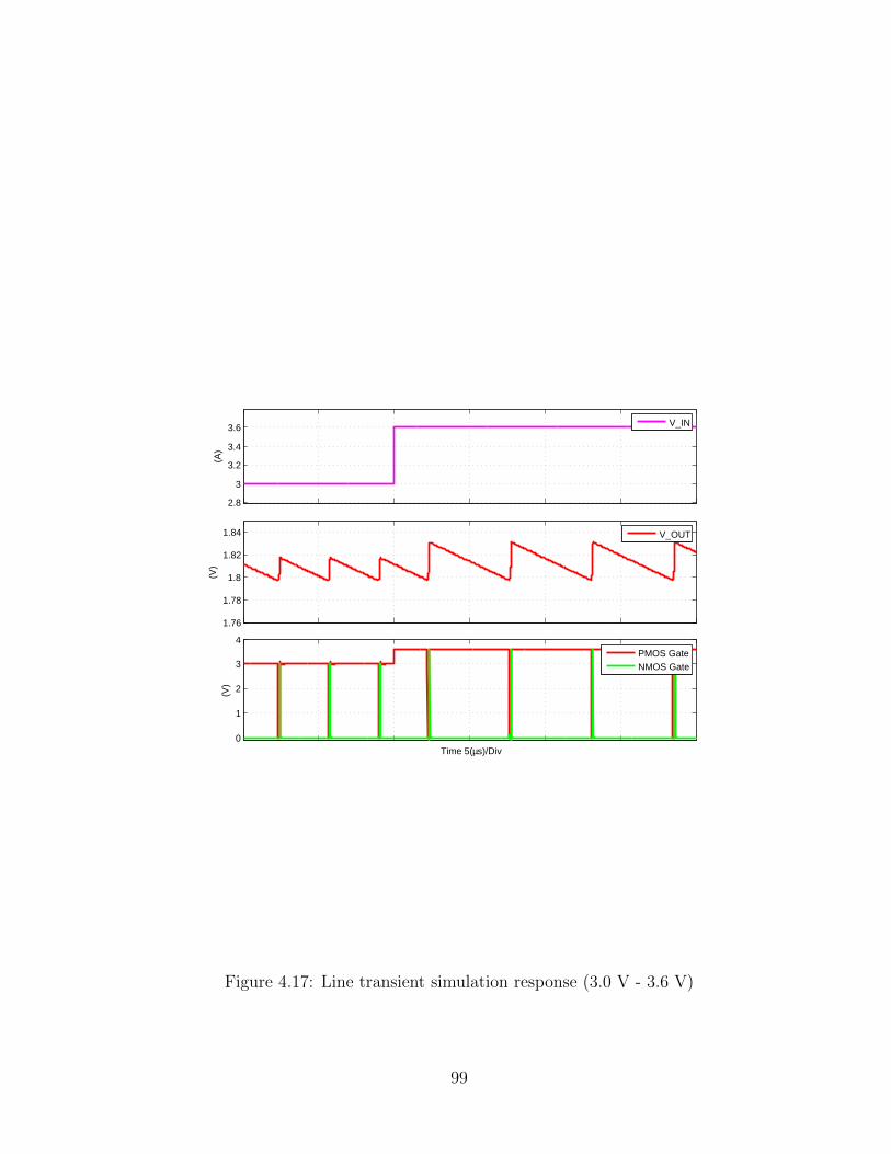
2.8
3
3.2
3.4
3.6
(A)
V_IN
1.76
1.78
1.8
1.82
1.84
(V)
V_OUT
0
1
2
3
4
(V)
Time 5(µs)/Div
PMOS GateNMOS Gate
Figure 4.17: Line transient simulation response (3.0 V - 3.6 V)
99

Chapter 5
HARDWARE IMPLEMENTATION AND MEASURED RESULTS
This chapter discusses the hardware implementation of the design. Layout of the
complete design and the individual block layouts are shown. Layout techniques
to prevent mismatch in the layout are also discussed. Finally, test results of the
fabricated chip are presented.
5.1 Layout
The complete layout with the pad frame is shown in Fig. 5.1. The padframe
consists of 40 pads, i.e., 40 I/O pins, and occupies an area of 1.5 mm × 1.5 mm.
Every pad occupies a length of 212.3 µm on each side, which leaves an active area
for layout of 1075.4 µm × 1075.4 µm.
The area consumed by this design, excluding the bias resistors, is 395.16 µm
× 89.34 µm. 21 out of 40 pins are used. The major area is consumed by on-chip
bias resistors of 50 MΩ and 2 MΩ for the comparator. The resistor model used
is ”oprrpresx”. The 50 MΩ resistor consumed an area of 565.44 µm × 302.04 µm
, whereas, the 2 MΩ resistor occupied an area of 150.04 µm × 97.24 µm. The
inductor and capacitor are off-chip and are not laid out.
The layouts of major blocks are shown in this section and the area con-
sumed by all the major blocks is summarized in Table 5.1.
For laying out the power switches, a gate strapping technique is used.
The gate of the MOSFET, which is siliced poly has high resistivity. This high
100
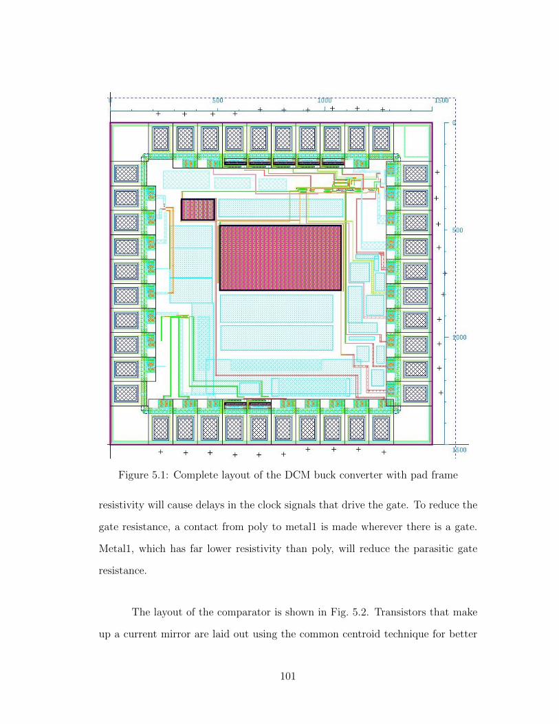
Figure 5.1: Complete layout of the DCM buck converter with pad frame
resistivity will cause delays in the clock signals that drive the gate. To reduce the
gate resistance, a contact from poly to metal1 is made wherever there is a gate.
Metal1, which has far lower resistivity than poly, will reduce the parasitic gate
resistance.
The layout of the comparator is shown in Fig. 5.2. Transistors that make
up a current mirror are laid out using the common centroid technique for better
101
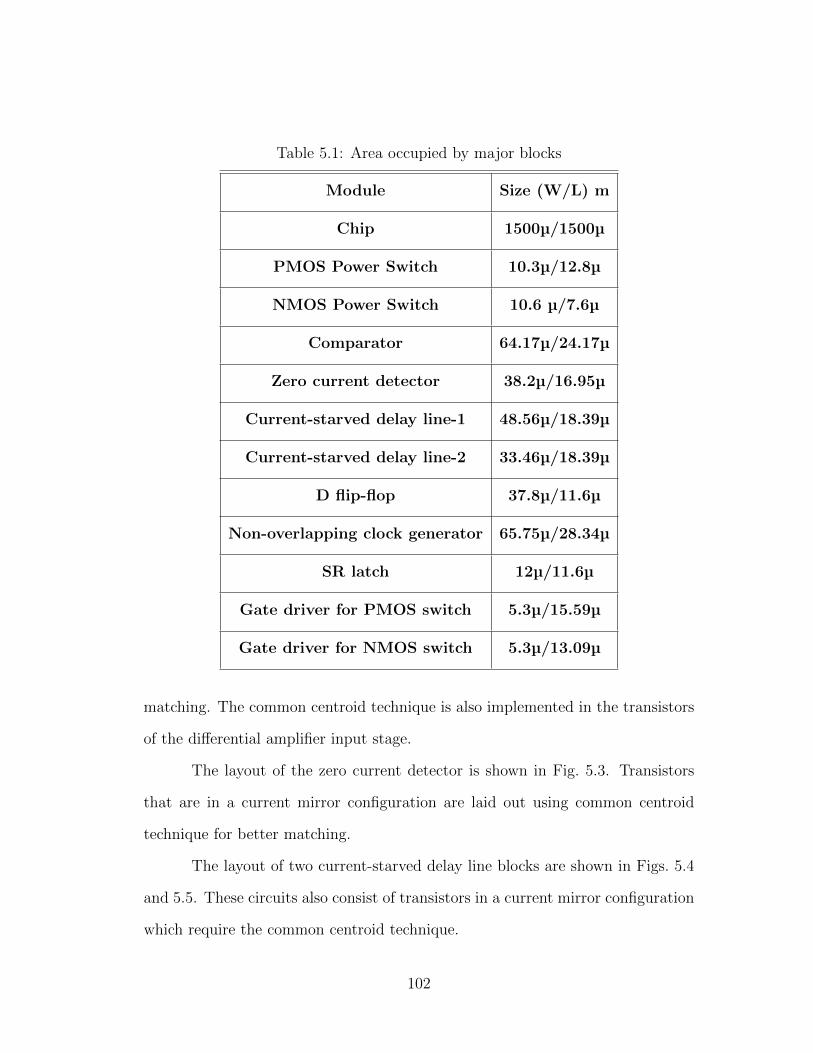
Table 5.1: Area occupied by major blocks
Module Size (W/L) m
Chip 1500µ/1500µ
PMOS Power Switch 10.3µ/12.8µ
NMOS Power Switch 10.6 µ/7.6µ
Comparator 64.17µ/24.17µ
Zero current detector 38.2µ/16.95µ
Current-starved delay line-1 48.56µ/18.39µ
Current-starved delay line-2 33.46µ/18.39µ
D flip-flop 37.8µ/11.6µ
Non-overlapping clock generator 65.75µ/28.34µ
SR latch 12µ/11.6µ
Gate driver for PMOS switch 5.3µ/15.59µ
Gate driver for NMOS switch 5.3µ/13.09µ
matching. The common centroid technique is also implemented in the transistors
of the differential amplifier input stage.
The layout of the zero current detector is shown in Fig. 5.3. Transistors
that are in a current mirror configuration are laid out using common centroid
technique for better matching.
The layout of two current-starved delay line blocks are shown in Figs. 5.4
and 5.5. These circuits also consist of transistors in a current mirror configuration
which require the common centroid technique.
102
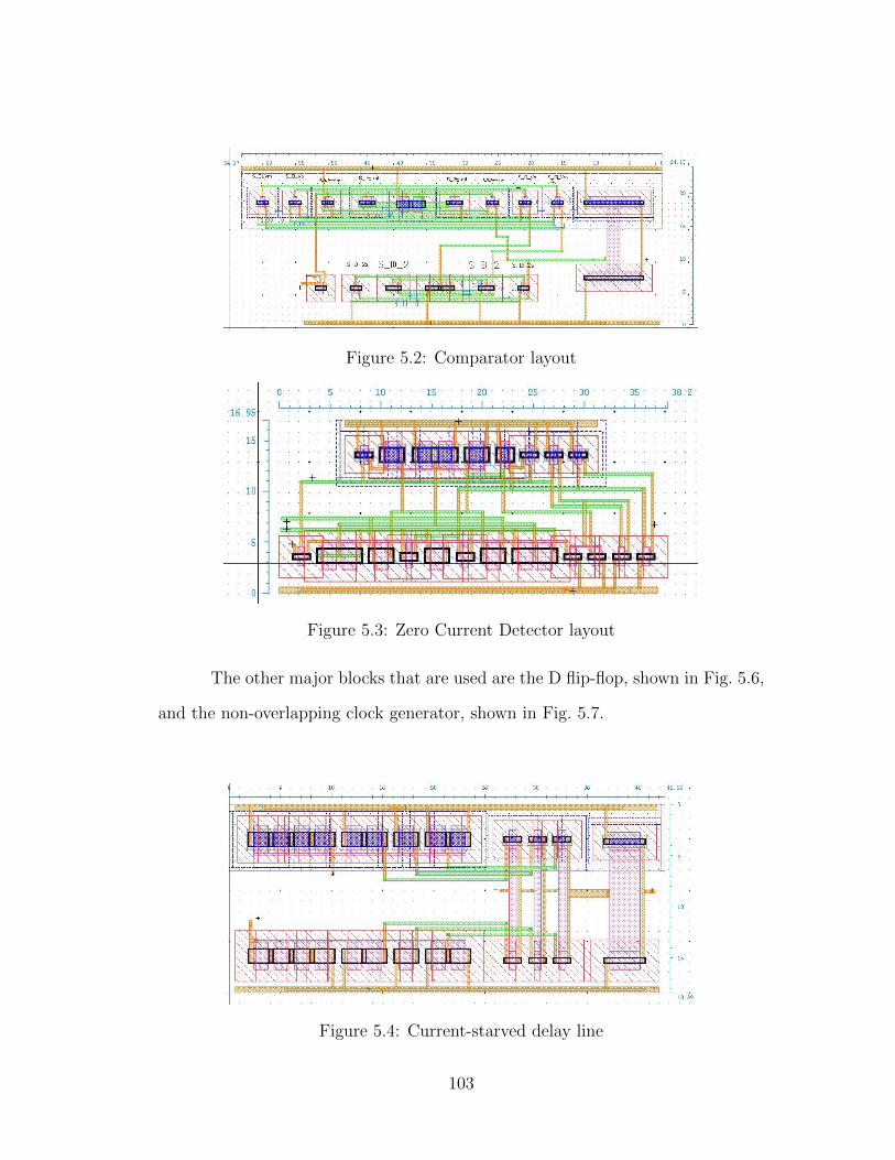
Figure 5.2: Comparator layout
Figure 5.3: Zero Current Detector layout
The other major blocks that are used are the D flip-flop, shown in Fig. 5.6,
and the non-overlapping clock generator, shown in Fig. 5.7.
Figure 5.4: Current-starved delay line
103
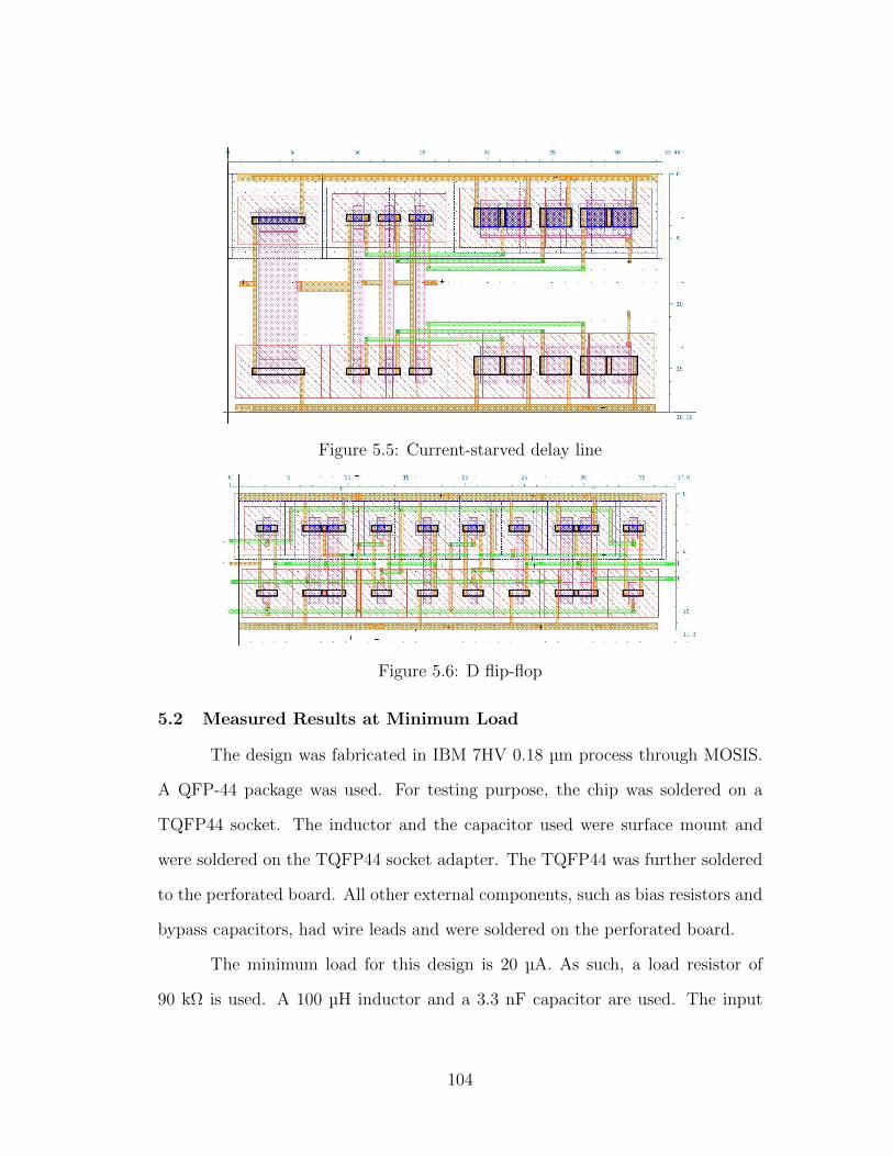
Figure 5.5: Current-starved delay line
Figure 5.6: D flip-flop
5.2 Measured Results at Minimum Load
The design was fabricated in IBM 7HV 0.18 µm process through MOSIS.
A QFP-44 package was used. For testing purpose, the chip was soldered on a
TQFP44 socket. The inductor and the capacitor used were surface mount and
were soldered on the TQFP44 socket adapter. The TQFP44 was further soldered
to the perforated board. All other external components, such as bias resistors and
bypass capacitors, had wire leads and were soldered on the perforated board.
The minimum load for this design is 20 µA. As such, a load resistor of
90 kΩ is used. A 100 µH inductor and a 3.3 nF capacitor are used. The input
104
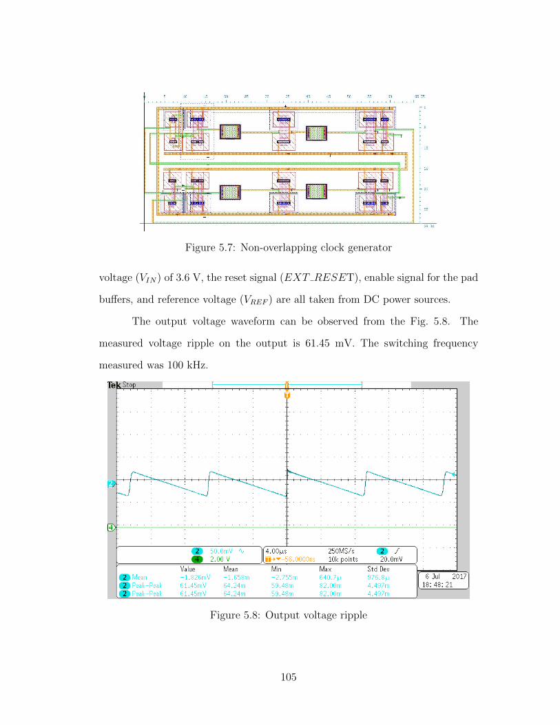
Figure 5.7: Non-overlapping clock generator
voltage (VIN) of 3.6 V, the reset signal (EXT RESET), enable signal for the pad
buffers, and reference voltage (VREF ) are all taken from DC power sources.
The output voltage waveform can be observed from the Fig. 5.8. The
measured voltage ripple on the output is 61.45 mV. The switching frequency
measured was 100 kHz.
Figure 5.8: Output voltage ripple
105
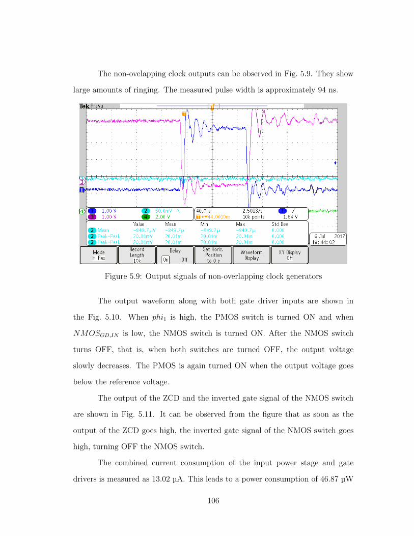
The non-ovelapping clock outputs can be observed in Fig. 5.9. They show
large amounts of ringing. The measured pulse width is approximately 94 ns.
Figure 5.9: Output signals of non-overlapping clock generators
The output waveform along with both gate driver inputs are shown in
the Fig. 5.10. When phi1 is high, the PMOS switch is turned ON and when
NMOSGD,IN is low, the NMOS switch is turned ON. After the NMOS switch
turns OFF, that is, when both switches are turned OFF, the output voltage
slowly decreases. The PMOS is again turned ON when the output voltage goes
below the reference voltage.
The output of the ZCD and the inverted gate signal of the NMOS switch
are shown in Fig. 5.11. It can be observed from the figure that as soon as the
output of the ZCD goes high, the inverted gate signal of the NMOS switch goes
high, turning OFF the NMOS switch.
The combined current consumption of the input power stage and gate
drivers is measured as 13.02 µA. This leads to a power consumption of 46.87 µW
106
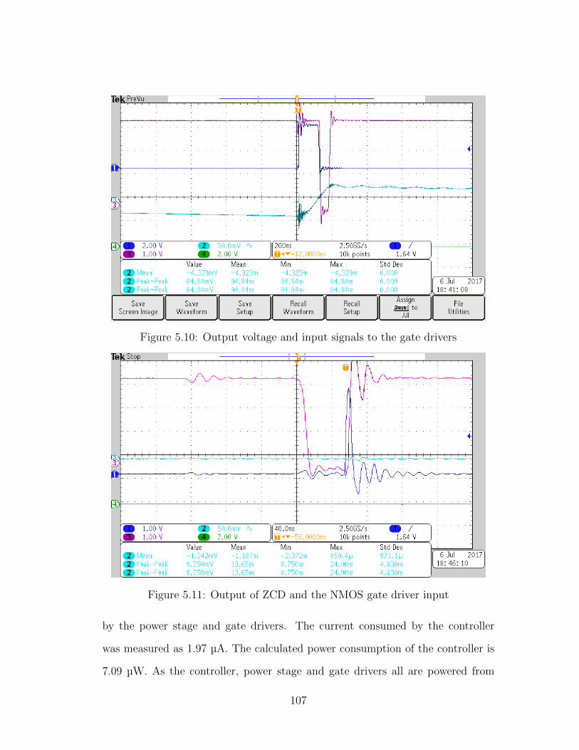
Figure 5.10: Output voltage and input signals to the gate drivers
Figure 5.11: Output of ZCD and the NMOS gate driver input
by the power stage and gate drivers. The current consumed by the controller
was measured as 1.97 µA. The calculated power consumption of the controller is
7.09 µW. As the controller, power stage and gate drivers all are powered from
107
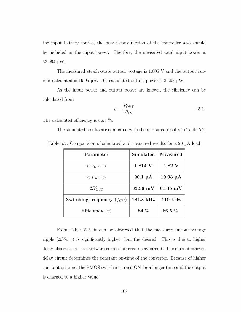
the input battery source, the power consumption of the controller also should
be included in the input power. Therfore, the measured total input power is
53.964 µW.
The measured steady-state output voltage is 1.805 V and the output cur-
rent calculated is 19.95 µA. The calculated output power is 35.93 µW.
As the input power and output power are known, the efficiency can be
calculated from
η ≡ POUT
PIN
(5.1)
The calculated efficiency is 66.5 %.
The simulated results are compared with the measured results in Table 5.2.
Table 5.2: Comparision of simulated and measured results for a 20 µA load
Parameter Simulated Measured
< VOUT > 1.814 V 1.82 V
< IOUT > 20.1 µA 19.93 µA
∆VOUT 33.36 mV 61.45 mV
Switching frequency (fSW ) 184.8 kHz 110 kHz
Efficiency (η) 84 % 66.5 %
From Table. 5.2, it can be observed that the measured output voltage
ripple (∆VOUT ) is significantly higher than the desired. This is due to higher
delay observed in the hardware current-starved delay circuit. The current-starved
delay circuit determines the constant on-time of the converter. Because of higher
constant on-time, the PMOS switch is turned ON for a longer time and the output
is charged to a higher value.
108
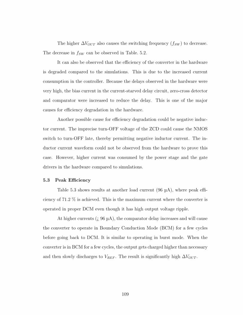
The higher ∆VOUT also causes the switching frequency (fSW ) to decrease.
The decrease in fSW can be observed in Table. 5.2.
It can also be observed that the efficiency of the converter in the hardware
is degraded compared to the simulations. This is due to the increased current
consumption in the controller. Because the delays observed in the hardware were
very high, the bias current in the current-starved delay circuit, zero-cross detector
and comparator were increased to reduce the delay. This is one of the major
causes for efficiency degradation in the hardware.
Another possible cause for efficiency degradation could be negative induc-
tor current. The imprecise turn-OFF voltage of the ZCD could cause the NMOS
switch to turn-OFF late, thereby permitting negative inductor current. The in-
ductor current waveform could not be observed from the hardware to prove this
case. However, higher current was consumed by the power stage and the gate
drivers in the hardware compared to simulations.
5.3 Peak Efficiency
Table 5.3 shows results at another load current (96 µA), where peak effi-
ciency of 71.2 % is achieved. This is the maximum current where the converter is
operated in proper DCM even though it has high output voltage ripple.
At higher currents (¿ 96 µA), the comparator delay increases and will cause
the converter to operate in Boundary Conduction Mode (BCM) for a few cycles
before going back to DCM. It is similar to operating in burst mode. When the
converter is in BCM for a few cycles, the output gets charged higher than necessary
and then slowly discharges to VREF . The result is significantly high ∆VOUT .
109
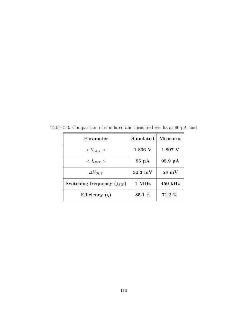
Table 5.3: Comparision of simulated and measured results at 96 µA load
Parameter Simulated Measured
< VOUT > 1.806 V 1.807 V
< IOUT > 96 µA 95.9 µA
∆VOUT 30.3 mV 58 mV
Switching frequency (fSW ) 1 MHz 450 kHz
Efficiency (η) 85.1 % 71.2 %
110
Chapter 6
CONCLUSIONS
6.1 Summary
Ultra-low power applications such as wearable devices have limitations on
their size and weight. The limitations on size and weight of these devices will also
impose limitations on the battery size used in these devices, which thereby limits
the amount of battery energy available. Therefore, it is important to efficiently
use the limited battery energy, in order to achieve longer battery life.
This work proposes a highly efficient DC-DC buck converter design for
ultra-low power applications in order to fulfill the above requirement. The design
was implemented in IBM 180-nm technology and fabricated with a QFP44 package
through MOSIS. The maximum efficiency achieved by the design in simulation is
87.1 % at 200 µA load with an input voltage of 3.6 V.
A ripple-based constant on-time control with DCM-enabling circuitry is
implemented. The DC-DC converter is operated in Discontinuous Conduction
Mode (DCM), which is favorable for light loads.
The control-loop is implemented with simple circuitry, which greatly re-
duces the area occupied by the converter. Various power reduction techniques
are implemented to reduce the power consumption in the controller. The ZCD
and comparator are the only analog circuits which are power hungry. However,
in this work, the ZCD is enabled by the NMOS gate signal so that it is turned
ON only for a short duration in each cycle, thereby reducing the average power
consumption in the ZCD. The PMOS to NMOS ratio in the digital circuits, which
111

is generally 2:1, is violated in order to reduce the power consumption in the digital
blocks. Instead, the PMOS to NMOS ratio in all digital circuits is maintained at
1:1.
6.2 Comparison with the State-of-the-Art
The simulation results of the proposed ultra-low power design are compared
with the other state-of-the art low power designs. The comparison results are
summarized in Table 6.1.
The proposed work used IBM 180 nm technology for the design. The design
converts an input DC voltage range of 2.8 V - 4.2 V to an output DC voltage of
1.8 V, where 2.8 V - 4.2 V is the voltage range of a li-ion battery. The load
currents, which are ultra-low, range from 20 µA - 200 µA. The output voltage
ripple (∆VOUT ) varies with the load current between 26.2 mV - 33.5 mV, where
the highest ripple is at 20 µA. ∆VOUT is < 2% across the entire load range. The
switching frequency ranges from 185 kHz at 20 µA to 1.7 MHz at 200 µA. The
inductor and capacitor values of 100 µH and 3.3 nF are fixed across the input
voltage range and output load current range. Another parameter that varies
across the load range is the power efficiency of the converter with 85.1 % at 20 µA
that increases as the load current increases. The peak efficiency of the converter
is 87.1 % at 200 µA load. The entire load range is operated with discontinuous
conduction mode.
In Table 6.1, three other works [2], [3], [13] on ultra-low power applications
are reported for comparison with the proposed work. Observing the output voltage
and load current range of these works, it can be inferred that these three works are
not limited only to ultra-low power. The applications of these other three works
range from ultra-low power to low-power, whereas the proposed work is only for
ultra-low power applications.
112

∆VOUT is not reported in any of these works. The work in [2] reports a
switching frequency (fSW ) of 32 Hz for ultra-low loads which is significantly low
compared to fSW of 185 kHz in the proposed design. Not only the proposed design
is faster than [2], but also has better regulation. fSW at 200 µA is not reported
in [2],but the maximum fSW is 2.5 MHz at 20 mA load current. The work in [3]
reports a fSW of 1.65 MHz at 200 µA load which similar to fSW of 1.7 MHz in
the proposed design.
The 100 µH inductor value chosen for this design is significantly large
compared to the inductor values of other works, but the size (3 mm x 3 mm x
1.3 mm) of the 100 µH inductor is within the typical range of inductor sizes that
are used. However, the inductor size is not reported by other works. The output
capacitor of this work is significantly lower compared to the other works.
Comparing the power efficiency, the proposed work reports a higher effi-
ciency across the entire load range compared to [2] and [3]. However, the work in
[13] achieves higher efficiency compared to the proposed design.
Because of their wide load current range, the works in [2] and [3] switched
the operating modes accordingly with the load current, whereas the proposed
design operates only in DCM across the entire load range.
6.3 Issues
The delay in the comparator is the major issue of this design, which limits
the maximum load current to 200 µA. As the load current increases, because of the
delay in the comparator, the converter begins to operate in Boundary Conduction
Mode (BCM) for a few cycles and then again to operate in DCM. Because of the
successive turn-ON of the PMOS switch in BCM, the output capacitor overcharges
and increases the output voltage ripple.
113
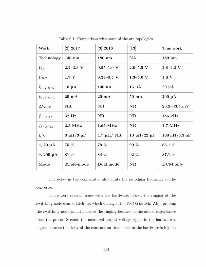
Table 6.1: Comparison with state-of-the-art topologies.
Work [2] 2017 [3] 2016 [13] This work
Technology 130 nm 180 nm NA 180 nm
VIN 2.2–3.3 V 0.55–1.0 V 2.0–5.5 V 2.8–4.2 V
VOUT 1.7 V 0.35–0.5 V 1.3–5.0 V 1.8 V
IOUT,MIN 10 µA 100 nA 15 µA 20 µA
IOUT,MAX 20 mA 20 mA 50 mA 200 µA
∆VOUT NR NR NR 26.2–33.5 mV
fSW,MIN 32 Hz NR NR 185 kHz
fSW,MAX 2.5 MHz 1.65 MHz NR 1.7 MHz
L/C 3 µH/3 µF 4.7 µH/ NR 10 µH/22 µF 100 µH/3.3 nF
η, 20 µA 75 % 79 % 90 % 85.1 %
η, 200 µA 81 % 84 % 92 % 87.1 %
Mode Triple-mode Dual mode NR DCM only
The delay in the comparator also limits the switching frequency of the
converter.
There were several issues with the hardware. First, the ringing at the
switching node caused latch-up, which damaged the PMOS switch. Also, probing
the switching node would increase the ringing because of the added capacitance
from the probe. Second, the measured output voltage ripple in the hardware is
higher because the delay of the constant on-time block in the hardware is higher.
114
Also, the delays of the comparator and the zero-current detector in the hardware
did not match with the simulation results.
6.4 Future Work
Ultra-low power applications like wearable devices always demand longer
battery life. With the increasing functionality, the power consumption also in-
creases, thereby degrading the battery run-time. This demands the DC-DC con-
verters to be more efficient.
Some ideas for the future work in ultra-low power DC-DC buck converter
are:
• The comparator used in this design can be replaced by an adaptively-biased
comparator, where the bias current for the comparator increases with the
load current. If implemented, the issue of operating in BCM for multiple
cycles will be solved, which helps in achieving a wider load current range.
• Adaptive on-time technique helps in achieving lower output voltage ripple.
• The negative inductor current in the buck converter, which will introduce
power losses, can be avoided if the ZCD is fast and precise. A ZCD imple-
mented with a comparator may not be precise because of the mismatch in
the hardware. In the future, we need to make the reference voltage attached
to the ZCD an external input, so that, through calibration, the mismatch
can be canceled.
put together...
• The reference voltage for the zero-current detector should be made pro-
grammable so that the zero-current detector turns OFF the NMOS switch
at the right time.
115

• Techniques to reduce ringing at the switching node could be explored. Talk
about the resistor and the effect of it...
116

REFERENCES
REFERENCES
[1] Z. Bi and W. Xia, “Modeling and simulation of dual-mode dc/dc buck con-
verter,” in 2010 Second International Conference on Computer Modeling and
Simulation. IEEE, 2010, pp. 371–375.
[2] Y. J. Park, J. H. Park, H. J. Kim, H. Ryu, S. Kim, Y. Pu, K. C. Hwang,
Y. Yang, M. Lee, and K. Y. Lee, “A design of a 92.4% efficiency triple mode
control dc 8211;dc buck converter with low power retention mode and adap-
tive zero current detector for iot/wearable applications,” IEEE Transactions
on Power Electronics, pp. 6946–6960, 2017.
[3] P. H. Chen, C. S. Wu, and K. C. Lin, “A 50 nw-to-10 mw output power
tri-mode digital buck converter with self-tracking zero current detection for
photovoltaic energy harvesting,” IEEE Journal of Solid-State Circuits, pp.
523–532, Feb 2016.
[4] R.J.Baker, CMOS Circuit Design, Layout, and Simulation, 3rd ed. Wiley-
IEEE Press, 2010.
[5] W.-H. K. Hylas Y. H. Lam and D. Ma, “Loop gain analysis and development
of high-speed high-accuracy current sensors for switching converters,” in Cir-
cuits and Systems, 2004. ISCAS ’04. Proceedings of the 2004 International
Symposium. IEEE, 2004, pp. 828–831.
118
[6] Wearable technology and IoT wearable devices. [Online]. Available:
1.)http://www.businessinsider.com/wearable-technology-iot-devices-2016-8,
Accessed:July5th,2017
[7] Advances in sensor technology, integration and power manage-
ment are enabling the future of wearable technology. [Online].
Available: 1.)https://www.dialog-semiconductor.com/sites/default/files/
enabling-the-future-of-wearable-technology.pdf.Accessed:January26,2017
[8] K.-H. Chen, Power Management Techniques for Integrated Circuit Design,
1st ed. John Wiley Sons, Incorporated, 2016.
[9] A. Paidimarri and A. P. Chandrakasan, “10.8 a buck converter with 240pw
quiescent power, 922017 IEEE International Solid-State Circuits Conference
(ISSCC). IEEE, Feb 2017, pp. 192–193.
[10] J. C. Tsai, T. Y. Huang, W. W. Lai, and K. H. Chen, “Dual modulation
technique for high efficiency in high-switching buck converters over a wide
load range,” IEEE Transactions on Circuits and Systems I: Regular Papers,
pp. 1671–1680, 2011.
[11] Achieving High Efficiency under Micro-Watt Loads with Switching Buck
DC-DC Converters. [Online]. Available: 1.)https://pdfs.semanticscholar.
org/bff3/afc2b58fed5f03b4902a6dcae3cd98741d85.pdf.Accessed:June6,2017
[12] Power Management Reference Design for a Wearable Device with
Wireless Charging Using the bq51003 and bq25120. [Online]. Available:
1.)http://www.ti.com/lit/ug/slua748a/slua748a.pdf,Accessed:July5th,2017
119

[13] TPS6273x Programmable Output Voltage Ultra-Low Power Buck Converter
With Up to 50 mA / 200 mA Output Current. [Online]. Available:
1.)http://www.ti.com/lit/ds/symlink/tps62736.pdf,Accessed:July5th,2017
120
![A Constant ON-Time 3-Level Buck Converter for Low Power ... · A Constant ON-Time 3-Level Buck Converter for Low Power ... ... a A / ]](https://img.pdfslide.us/doc/110x75/5beeed8009d3f25b348b4e6c/a-constant-on-time-3-level-buck-converter-for-low-power-a-constant-on-time.jpg)