Embed Size (px)
Citation preview
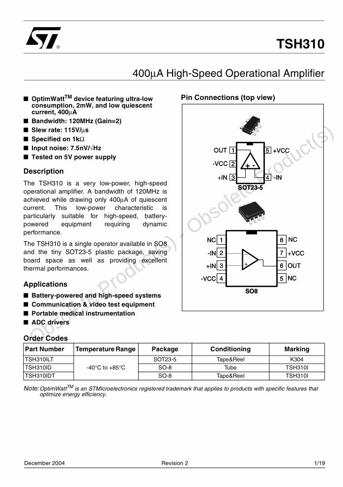
TSH310
400µA High-Speed Operational Amplifier
OptimWattTM device featuring ultra-low consumption, 2mW, and low quiescent current, 400µA
Bandwidth: 120MHz (Gain=2) Slew rate: 115V/µs Specified on 1kΩ Input noise: 7.5nV/√Hz Tested on 5V power supply
Description
The TSH310 is a very low-power, high-speedoperational amplifier. A bandwidth of 120MHz isachieved while drawing only 400µA of quiescentcurrent. This low-power characteristic isparticularly suitable for high-speed, battery-powered equipment requiring dynamicperformance.
The TSH310 is a single operator available in SO8and the tiny SOT23-5 plastic package, savingboard space as well as providing excellentthermal performances.
Applications
Battery-powered and high-speed systems Communication & video test equipment Portable medical instrumentation ADC drivers
Pin Connections (top view)
Order Codes
Note:OptimWattTM is an STMIcroelectronics registered trademark that applies to products with specific features that optimize energy efficiency.
1
2
3
5
4
-VCC
+VCC
+ -
OUT
-IN+IN
SOT23-5
+VCC
1
2
3
54
8
7
6
NC
OUT+
_
-VCC
NC
-IN
+IN
SO8
NC
1
2
3
5
4
-VCC
+VCC
+ -
OUT
-IN+IN
SOT23-5
+VCC
1
2
3
54
8
7
6
NC
OUT+
_
-VCC
NC
-IN
+IN
SO8
NC
Part Number Temperature Range Package Conditioning Marking
TSH310ILT-40°C to +85°C
SOT23-5 Tape&Reel K304TSH310ID SO-8 Tube TSH310ITSH310IDT SO-8 Tape&Reel TSH310I
Obso
lete Product(s)
- Obso
lete Product(s)
December 2004 Revision 2 1/19
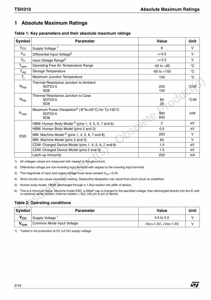
TSH310 Absolute Maximum Ratings
1 Absolute Maximum Ratings
Table 1: Key parameters and their absolute maximum ratings
Symbol Parameter Value Unit
VCC Supply Voltage 1
1) All voltages values are measured with respect to the ground pin.
6 V
Vid Differential Input Voltage2
2) Differential voltage are non-inverting input terminal with respect to the inverting input terminal.
+/-0.5 V
Vin Input Voltage Range3
3) The magnitude of input and output voltage must never exceed VCC +0.3V.
+/-2.5 V
Toper Operating Free Air Temperature Range -40 to +85 °C
Tstg Storage Temperature -65 to +150 °C
Tj Maximum Junction Temperature 150 °C
Rthja
Thermal Resistance Junction to Ambient SOT23-5SO8
250150
°C/W
Rthjc
Thermal Resistance Junction to CaseSOT23-5SO8
8028
°C/W
Pmax
Maximum Power Dissipation4 (@Ta=25°C) for Tj=150°CSOT23-5SO8
4) Short-circuits can cause excessive heating. Destructive dissipation can result from short circuit on amplifiers.
500830
mW
ESD
HBM: Human Body Model 5 (pins 1, 4, 5, 6, 7 and 8)
5) Human body model, 100pF discharged through a 1.5kΩ resistor into pMin of device.
2 kV
HBM: Human Body Model (pins 2 and 3) 0.5 kV
MM: Machine Model 6 (pins 1, 4, 5, 6, 7 and 8)
6) This is a minimum Value. Machine model ESD, a 200pF cap is charged to the specified voltage, then discharged directly into the IC withno external series resistor (internal resistor < 5Ω), into pin to pin of device.
200 V
MM: Machine Model (pins 2 and 3) 60 VCDM: Charged Device Model (pins 1, 4, 5, 6, 7 and 8) 1.5 kVCDM: Charged Device Model (pins 2 and 3) 1.5 kV
Latch-up Immunity 200 mA
Table 2: Operating conditions
Symbol Parameter Value Unit
VCC Supply Voltage 1
1) Tested in full production at 5V (±2.5V) supply voltage.
4.5 to 5.5 V
Vicm Common Mode Input Voltage -Vcc+1.5V, +Vcc-1.5V V
Obsolete Product(
s) - O
bsolete Product(
s)
2/19
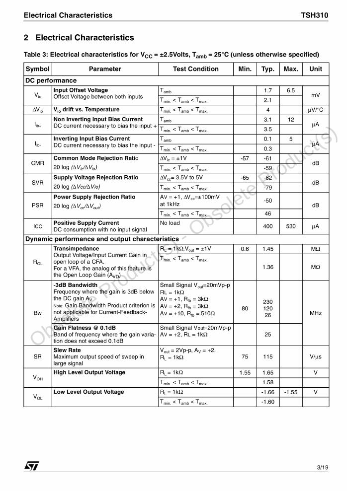
Electrical Characteristics TSH310
2 Electrical Characteristics
Table 3: Electrical characteristics for VCC = ±2.5Volts, Tamb = 25°C (unless otherwise specified)
Symbol Parameter Test Condition Min. Typ. Max. Unit
DC performance
Vio
Input Offset VoltageOffset Voltage between both inputs
Tamb 1.7 6.5mV
Tmin. < Tamb < Tmax. 2.1
∆Vio Vio drift vs. Temperature Tmin. < Tamb < Tmax. 4 µV/°C
Iib+
Non Inverting Input Bias CurrentDC current necessary to bias the input +
Tamb 3.1 12µA
Tmin. < Tamb < Tmax. 3.5
Iib-
Inverting Input Bias CurrentDC current necessary to bias the input -
Tamb 0.1 5µA
Tmin. < Tamb < Tmax. 0.3
CMRCommon Mode Rejection Ratio
20 log (∆Vic/∆Vio)
∆Vic = ±1V -57 -61dB
Tmin. < Tamb < Tmax. -59
SVRSupply Voltage Rejection Ratio
20 log (∆Vcc/∆Vio)
∆Vcc= 3.5V to 5V -65 -82dB
Tmin. < Tamb < Tmax. -79
PSR
Power Supply Rejection Ratio
20 log (∆Vcc/∆Vout)
AV = +1, ∆Vcc=±100mV at 1kHz
-50dB
Tmin. < Tamb < Tmax. 46
ICCPositive Supply CurrentDC consumption with no input signal
No load400 530 µA
Dynamic performance and output characteristics
ROL
TransimpedanceOutput Voltage/Input Current Gain in open loop of a CFA.For a VFA, the analog of this feature is the Open Loop Gain (AVD)
RL = 1kΩ,Vout = ±1V 0.6 1.45 MΩ
Tmin. < Tamb < Tmax.
1.36 MΩ
Bw
-3dB BandwidthFrequency where the gain is 3dB below the DC gain AV
Note: Gain Bandwidth Product criterion is not applicable for Current-Feedback-Amplifiers
Small Signal Vout=20mVp-pRL = 1kΩAV = +1, Rfb = 3kΩAV = +2, Rfb = 3kΩAV = +10, Rfb = 510Ω
8023012026 MHz
Gain Flatness @ 0.1dBBand of frequency where the gain varia-tion does not exceed 0.1dB
Small Signal Vout=20mVp-pAV = +2, RL = 1kΩ 25
SRSlew RateMaximum output speed of sweep in large signal
Vout = 2Vp-p, AV = +2, RL = 1kΩ 75 115 V/µs
VOH
High Level Output Voltage RL = 1kΩ 1.55 1.65 V
Tmin. < Tamb < Tmax. 1.58
VOL
Low Level Output Voltage RL = 1kΩ -1.66 -1.55 V
Tmin. < Tamb < Tmax. -1.60
Obso
lete Product(s)
- Obso
lete Product(s)
3/19
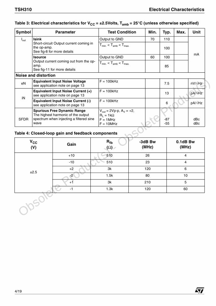
TSH310 Electrical Characteristics
Iout IsinkShort-circuit Output current coming in the op-amp.See fig-8 for more details
Output to GND 70 110
mA
Tmin. < Tamb < Tmax.100
IsourceOutput current coming out from the op-amp.See fig-11 for more details
Output to GND 60 100
Tmin. < Tamb < Tmax.85
Noise and distortion
eNEquivalent Input Noise Voltagesee application note on page 13
F = 100kHz7.5 nV/√Hz
iN
Equivalent Input Noise Current (+)see application note on page 13
F = 100kHz13 pA/√Hz
Equivalent Input Noise Current (-)see application note on page 13
F = 100kHz6 pA/√Hz
SFDR
Spurious Free Dynamic RangeThe highest harmonic of the output spectrum when injecting a filtered sine wave
Vout = 2Vp-p, AV = +2, RL = 1kΩF = 1MHzF = 10MHz
-87-55
dBcdBc
Table 4: Closed-loop gain and feedback components
VCC
(V)Gain
Rfb (Ω)
-3dB Bw(MHz)
0.1dB Bw(MHz)
±2.5
+10 510 26 4
-10 510 23 4
+2 3k 120 6
-2 1.5k 80 10
+1 3k 210 5
-1 1.3k 120 60
Table 3: Electrical characteristics for VCC = ±2.5Volts, Tamb = 25°C (unless otherwise specified)
Symbol Parameter Test Condition Min. Typ. Max. Unit
Obso
lete Product(s)
- Obso
lete Product(s)
4/19
Electrical Characteristics TSH310
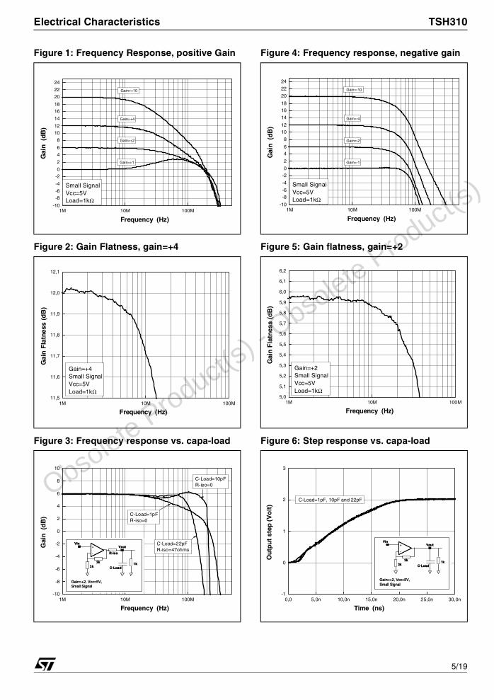
Figure 1: Frequency Response, positive Gain
Figure 2: Gain Flatness, gain=+4
Figure 3: Frequency response vs. capa-load
1M 10M 100M-10
-8-6
-4
-20
2
46
8
1012
14
1618
20
22
24
Gain=+1
Gain=+2
Gain=+4
Small SignalVcc=5VLoad=1kΩ
Gain=+10
Gai
n (
dB)
Frequency (Hz)
1M 10M 100M11,5
11,6
11,7
11,8
11,9
12,0
12,1
Gain=+4Small SignalVcc=5VLoad=1kΩ
Gai
n F
latn
ess
(dB
)
Frequency (Hz)
1M 10M 100M-10
-8
-6
-4
-2
0
2
4
6
8
10
+
-
3k3k
VinVout
Gain=+2, Vcc=5V, Small Signal
1kC-Load
R-iso
+
-
3k3k
VinVout
Gain=+2, Vcc=5V, Small Signal
1kC-Load
R-iso
C-Load=10pFR-iso=0
C-Load=22pFR-iso=47ohms
C-Load=1pFR-iso=0
Gai
n (
dB
)
Frequency (Hz)
Figure 4: Frequency response, negative gain
Figure 5: Gain flatness, gain=+2
Figure 6: Step response vs. capa-load
1M 10M 100M-10
-8-6
-4
-20
2
46
8
1012
14
1618
20
22
24
Gain=-1
Gain=-2
Gain=-4
Small SignalVcc=5VLoad=1kΩ
Gain=-10
Gai
n (
dB)
Frequency (Hz)
1M 10M 100M5,0
5,1
5,2
5,3
5,4
5,5
5,6
5,7
5,8
5,9
6,0
6,1
6,2
Gain=+2Small SignalVcc=5VLoad=1kΩ
Gai
n F
latn
ess
(dB
)
Frequency (Hz)
0,0 5,0n 10,0n 15,0n 20,0n 25,0n 30,0n-1
0
1
2
3
+
-
3k3k
VinVout
Gain=+2, Vcc=5V, Small Signal
1kC-Load
+
-
3k3k
VinVout
Gain=+2, Vcc=5V, Small Signal
1kC-Load
C-Load=1pF, 10pF and 22pF
Ou
tpu
t st
ep (
Vo
lt)
Time (ns)
Obso
lete Product(s)
- Obso
lete Product(s)
5/19
TSH310 Electrical Characteristics
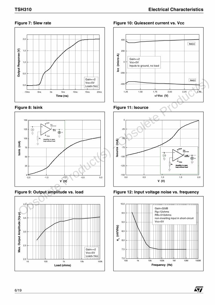
Figure 7: Slew rate
Figure 8: Isink
Figure 9: Output amplitude vs. load
-10ns -5ns 0s 5ns 10ns 15ns 20ns
0,0
0,5
1,0
1,5
2,0
Gain=+2Vcc=5VLoad=1kΩ
Ou
tput
Res
po
nse
(V
)
Time (ns)
-2,0 -1,5 -1,0 -0,5 0,00
25
50
75
100
125
150
+
_
RG
+2.5V
- 2.5V
VOL without load
VIsink
Amplifier in open loop without load
-1V
+
_
RG
+2.5V
- 2.5V
VOL without load
VIsink
Amplifier in open loop without load
-1V
Isin
k (
mA
)
V (V)
10 100 1k 10k 100k2,0
2,5
3,0
3,5
4,0
Gain=+2Vcc=5VLoad=1kΩ
Max
. Ou
tpu
t A
mp
litu
de (
Vp-
p)
Load (ohms)
Figure 10: Quiescent current vs. Vcc
Figure 11: Isource
Figure 12: Input voltage noise vs. frequency
1,25 1,50 1,75 2,00 2,25 2,50
-400
-200
0
200
400
Gain=+2Vcc=5VInputs to ground, no load
Icc
(m
icro
-A)
Icc(+)
Icc(-)
+/-Vcc (V)
0,0 0,5 1,0 1,5 2,0-150
-125
-100
-75
-50
-25
0
+
_
RG
+2.5V
- 2.5V
VOH without load
V
Isource
Amplifier in open loop without load
+1V
+
_
RG
+2.5V
- 2.5V
VOH without load
V
Isource
Amplifier in open loop without load
+1VIso
urc
e (
mA
)
V (V)
100 1k 10k 100k 1M 10M 100M7,0
7,5
8,0
8,5
9,0
9,5
10,0
Gain=32dBRg=12ohmsRfb=510ohmsnon-inverting input in short-circuit Vcc=5V
e n (
nV/V
Hz)
Frequency (Hz)
Obso
lete Product(s)
- Obso
lete Product(s)
6/19
Electrical Characteristics TSH310
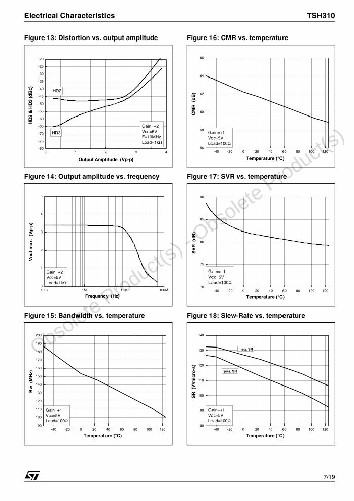
Figure 13: Distortion vs. output amplitude
Figure 14: Output amplitude vs. frequency
Figure 15: Bandwidth vs. temperature
0 1 2 3 4-80
-75
-70
-65
-60
-55
-50
-45
-40
-35
-30
-25
-20
HD3
HD2
Gain=+2Vcc=5VF=10MHzLoad=1kΩ
HD
2 &
HD
3 (d
Bc)
Output Amplitude (Vp-p)
100k 1M 10M 100M0
1
2
3
4
5
Gain=+2Vcc=5VLoad=1kΩ
Vou
t m
ax.
(Vp
-p)
Frequency (Hz)
-40 -20 0 20 40 60 80 100 12090
100
110
120
130
140
150
160
170
180
190
200
Gain=+1Vcc=5VLoad=100Ω
Bw
(M
Hz)
Temperature (°C)
Figure 16: CMR vs. temperature
Figure 17: SVR vs. temperature
Figure 18: Slew-Rate vs. temperature
-40 -20 0 20 40 60 80 100 12056
58
60
62
64
66
Gain=+1Vcc=5VLoad=100Ω
CM
R (
dB)
Temperature (°C)
-40 -20 0 20 40 60 80 100 12070
75
80
85
90
Gain=+1Vcc=5VLoad=100Ω
SV
R (
dB
)
Temperature (°C)
-40 -20 0 20 40 60 80 100 12080
90
100
110
120
130
140
neg. SR
pos. SR
Gain=+1Vcc=5VLoad=100Ω
SR
(V
/mic
ro-s
)
Temperature (°C)
Obso
lete Product(s)
- Obso
lete Product(s)
7/19
TSH310 Electrical Characteristics
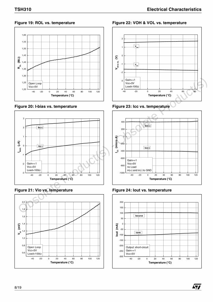
Figure 19: ROL vs. temperature
Figure 20: I-bias vs. temperature
Figure 21: Vio vs. temperature
-40 -20 0 20 40 60 80 100 1201,20
1,25
1,30
1,35
1,40
1,45
1,50
1,55
1,60
Open LoopVcc=5V
RO
L (
MΩ
)
Temperature (°C)
-40 -20 0 20 40 60 80 100 120-3
-2
-1
0
1
2
3
Gain=+1Vcc=5VLoad=100Ω
I BIA
S (µA
)
Ib(+)
Ib(-)
Temperature (°C)
-40 -20 0 20 40 60 80 100 120
0,6
0,8
1,0
1,2
1,4
1,6
1,8
2,0
Open LoopVcc=5VLoad=100Ω
Temperature (°C)
VIO
(m
V)
Figure 22: VOH & VOL vs. temperature
Figure 23: Icc vs. temperature
Figure 24: Iout vs. temperature
-40 -20 0 20 40 60 80-4
-3
-2
-1
0
1
2
Gain=+1Vcc=5VLoad=100Ω
VOL
VOH
VO
H &
OL (
V)
Temperature (°C)
-40 -20 0 20 40 60 80 100 120-1000
-800
-600
-400
-200
0
200
400
Gain=+1Vcc=5Vno Loadin(+) and in(-) to GND
Icc(+)
Icc(-)
Temperature (°C)
I CC (
mic
ro A
)
-40 -20 0 20 40 60 80 100 120-300
-250
-200
-150
-100
-50
0
50
100
150
200
Output: short-circuitGain=+1Vcc=5V
Iout
(m
A)
Isource
Isink
Temperature (°C)
Obso
lete Product(s)
- Obso
lete Product(s)
8/19
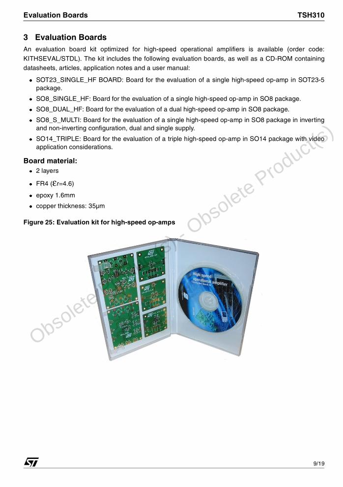
Evaluation Boards TSH310
3 Evaluation BoardsAn evaluation board kit optimized for high-speed operational amplifiers is available (order code:
KITHSEVAL/STDL). The kit includes the following evaluation boards, as well as a CD-ROM containingdatasheets, articles, application notes and a user manual:
SOT23_SINGLE_HF BOARD: Board for the evaluation of a single high-speed op-amp in SOT23-5package.
SO8_SINGLE_HF: Board for the evaluation of a single high-speed op-amp in SO8 package.
SO8_DUAL_HF: Board for the evaluation of a dual high-speed op-amp in SO8 package.
SO8_S_MULTI: Board for the evaluation of a single high-speed op-amp in SO8 package in invertingand non-inverting configuration, dual and single supply.
SO14_TRIPLE: Board for the evaluation of a triple high-speed op-amp in SO14 package with videoapplication considerations.
Board material: 2 layers
FR4 (εr=4.6)
epoxy 1.6mm
copper thickness: 35µm
Figure 25: Evaluation kit for high-speed op-amps
Obso
lete Product(s)
- Obso
lete Product(s)
9/19
TSH310 Power Supply Considerations
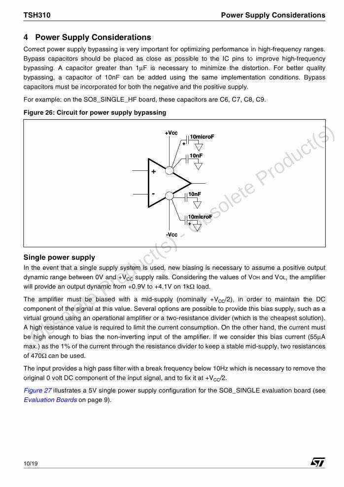
4 Power Supply ConsiderationsCorrect power supply bypassing is very important for optimizing performance in high-frequency ranges.
Bypass capacitors should be placed as close as possible to the IC pins to improve high-frequencybypassing. A capacitor greater than 1µF is necessary to minimize the distortion. For better quality
bypassing, a capacitor of 10nF can be added using the same implementation conditions. Bypass
capacitors must be incorporated for both the negative and the positive supply.
For example: on the SO8_SINGLE_HF board, these capacitors are C6, C7, C8, C9.
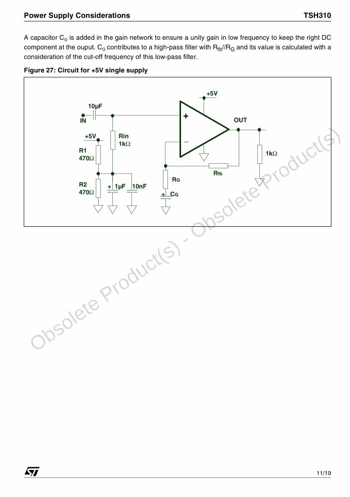
Single power supply In the event that a single supply system is used, new biasing is necessary to assume a positive output
dynamic range between 0V and +VCC supply rails. Considering the values of VOH and VOL, the amplifier
will provide an output dynamic from +0.9V to +4.1V on 1kΩ load.
The amplifier must be biased with a mid-supply (nominally +VCC/2), in order to maintain the DC
component of the signal at this value. Several options are possible to provide this bias supply, such as avirtual ground using an operational amplifier or a two-resistance divider (which is the cheapest solution).
A high resistance value is required to limit the current consumption. On the other hand, the current must
be high enough to bias the non-inverting input of the amplifier. If we consider this bias current (55µA
max.) as the 1% of the current through the resistance divider to keep a stable mid-supply, two resistances
of 470Ω can be used.
The input provides a high pass filter with a break frequency below 10Hz which is necessary to remove the
original 0 volt DC component of the input signal, and to fix it at +VCC/2.
Figure 27 illustrates a 5V single power supply configuration for the SO8_SINGLE evaluation board (see
Evaluation Boards on page 9).
Figure 26: Circuit for power supply bypassing
+
-VCC
+VCC10microF
+
10nF
10microF+
10nF-
+
-VCC
+VCC10microF
+
10nF
10microF+
10nF-
Obso
lete Product(s)
- Obso
lete Product(s)
10/19
Power Supply Considerations TSH310
A capacitor CG is added in the gain network to ensure a unity gain in low frequency to keep the right DC
component at the ouput. CG contributes to a high-pass filter with Rfb//RG and its value is calculated with a
consideration of the cut-off frequency of this low-pass filter.
Figure 27: Circuit for +5V single supply
RG
IN
+5V
Rfb
10µF
+ 1µF
+5V
10nF
Rin1kΩ
OUT
R1470Ω
R2470Ω
1kΩ
+
_
+ CG
Obso
lete Product(s)
- Obso
lete Product(s)
11/19
TSH310 Noise Measurements
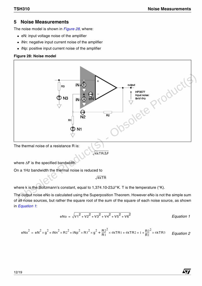
5 Noise MeasurementsThe noise model is shown in Figure 28, where:
eN: input voltage noise of the amplifier
iNn: negative input current noise of the amplifier
iNp: positive input current noise of the amplifier
The thermal noise of a resistance R is:
where ∆F is the specified bandwidth.
On a 1Hz bandwidth the thermal noise is reduced to
where k is the Boltzmann's constant, equal to 1,374.10-23J/°K. T is the temperature (°K).
The output noise eNo is calculated using the Superposition Theorem. However eNo is not the simple sum
of all noise sources, but rather the square root of the sum of the square of each noise source, as shown
in Equation 1:
Equation 1
Equation 2
Figure 28: Noise model
+
_
R3
R1
output
R2
iN-
iN+
HP3577Input noise:8nV/√Hz
N1
N2
N3 eN
+
_
R3
R1
output
R2
iN-
iN+
HP3577Input noise:8nV/√Hz
N1
N2
N3 eN
4kTR∆F
4kTR
eNo V12
V22
V32
V42
V52
V62
+ + + + +=
eNo2
eN2
g2
iNn2
R22
iNp2
+×+× R32
× g2
× R2R1-------
24kTR1 4kTR2 1 R2
R1-------+
24kTR3×+ +×+=
Obso
lete Product(s)
- Obso
lete Product(s)
12/19
Noise Measurements TSH310
The input noise of the instrumentation must be extracted from the measured noise value. The real output
noise value of the driver is:
Equation 3
The input noise is called the Equivalent Input Noise as it is not directly measured but is evaluated from the
measurement of the output divided by the closed loop gain (eNo/g).
After simplification of the fourth and the fifth term of Equation 2 we obtain:
Equation 4
Measurement of the input voltage noise eNIf we assume a short-circuit on the non-inverting input (R3=0), from Equation 4 we can derive:
Equation 5
In order to easily extract the value of eN, the resistance R2 will be chosen to be as low as possible. In theother hand, the gain must be large enough:
R3=0, gain: g=100
Measurement of the negative input current noise iNnTo measure the negative input current noise iNn, we set R3=0 and use Equation 5. This time the gain
must be lower in order to decrease the thermal noise contribution:
R3=0, gain: g=10
Measurement of the positive input current noise iNpTo extract iNp from Equation 3, a resistance R3 is connected to the non-inverting input. The value of R3
must be chosen in order to keep its thermal noise contribution as low as possible against the iNp
contribution:
R3=100Ω, gain: g=10
eNo Measured( )2 instrumentation( )2–=
eNo2
eN2
g2
iNn2
R22
iNp2
+×+× R32× g
2× g 4kTR2 1 R2R1-------+
24kTR3×+×+=
eNo eN2
g2
iNn2
R22
g 4kTR2×+×+×=
Obso
lete Product(s)
- Obso
lete Product(s)
13/19
TSH310 Intermodulation Distortion Product
6 Intermodulation Distortion ProductThe non-ideal output of the amplifier can be described by the following series:
due to non-linearity in the input-output amplitude transfer, where the input is Vin=Asinωt, C0 is the DC
component, C1(Vin) is the fundamental and Cn is the amplitude of the harmonics of the output signal Vout.
A one-frequency (one-tone) input signal contributes to harmonic distortion. A two-tone input signal
contributes to harmonic distortion and to the intermodulation product.
The study of the intermodulation and distortion for a two-tone input signal is the first step in characterizing
the driving capability of multi-tone input signals.
In this case:
then:
From this expression, we can extract the distortion terms, and the intermodulation terms form a single
sine wave: second-order intermodulation terms IM2 by the frequencies (ω1-ω2) and (ω1+ω2) with an
amplitude of C2A2 and third-order intermodulation terms IM3 by the frequencies (2ω1-ω2), (2ω1+ω2), (−ω1+2ω2) and (ω1+2ω2) with an amplitude of (3/4)C3A3.
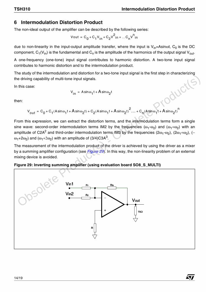
The measurement of the intermodulation product of the driver is achieved by using the driver as a mixer
by a summing amplifier configuration (see Figure 29). In this way, the non-linearity problem of an externalmixing device is avoided.
Figure 29: Inverting summing amplifier (using evaluation board SO8_S_MULTI)
Vout C0 C1Vin C2V2
in …CnVn
in+ + +=
Vin A ω1tsin A ω2tsin+=
Vout C0 C1 A ω1tsin A ω2tsin+( ) C2 A ω1tsin A ω2tsin+( )2… Cn A ω1tsin A ω2tsin+( )
n+ + +=
+
_
R
Rfb
1kΩ
Vout
R2Vin2
Vin1 R1
+
_
R
Rfb
1kΩ
Vout
R2Vin2
Vin1 R1
Obso
lete Product(s)
- Obso
lete Product(s)
14/19
The Bias of an Inverting Amplifier TSH310
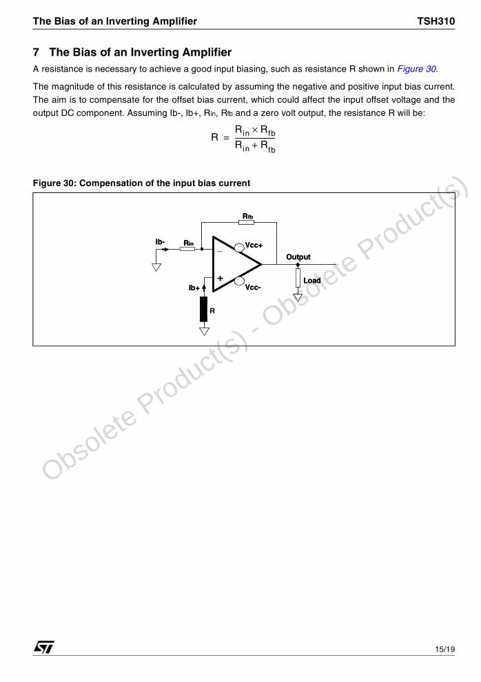
7 The Bias of an Inverting AmplifierA resistance is necessary to achieve a good input biasing, such as resistance R shown in Figure 30.
The magnitude of this resistance is calculated by assuming the negative and positive input bias current.
The aim is to compensate for the offset bias current, which could affect the input offset voltage and the
output DC component. Assuming Ib-, Ib+, Rin, Rfb and a zero volt output, the resistance R will be:
Figure 30: Compensation of the input bias current
RRin Rfb×Rin R+
fb
-----------------------=
R
Load
Output
Rfb
RinIb-
Ib+
Vcc+
Vcc-+
_
R
Load
Output
Rfb
RinIb-
Ib+
Vcc+
Vcc-+
_
Obso
lete Product(s)
- Obso
lete Product(s)
15/19
TSH310 Active Filtering
8 Active Filtering
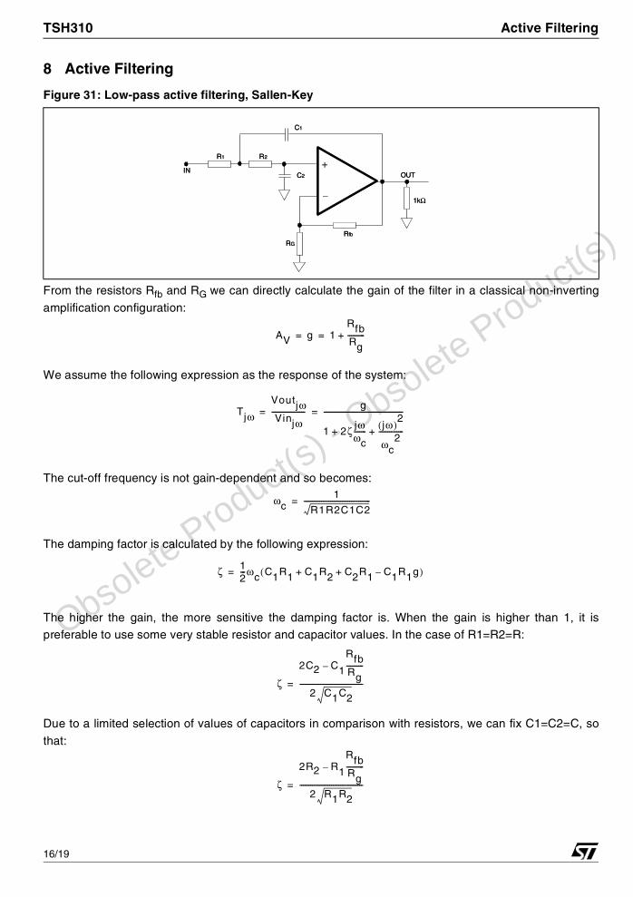
From the resistors Rfb and RG we can directly calculate the gain of the filter in a classical non-inverting
amplification configuration:
We assume the following expression as the response of the system:
The cut-off frequency is not gain-dependent and so becomes:
The damping factor is calculated by the following expression:
The higher the gain, the more sensitive the damping factor is. When the gain is higher than 1, it ispreferable to use some very stable resistor and capacitor values. In the case of R1=R2=R:
Due to a limited selection of values of capacitors in comparison with resistors, we can fix C1=C2=C, so
that:
Figure 31: Low-pass active filtering, Sallen-Key
+
_
RG
IN
Rfb
1kΩ
OUT
R1 R2
C2
C1
+
_
RG
IN
Rfb
1kΩ
OUT
R1 R2
C2
C1
AV g 1RfbRg----------+= =
TjωVoutjωVinjω
-------------------g
1 2ζ jωωc-------
jω( )2
ωc2
--------------+ +
---------------------------------------------= =
ωc1
R1R2C1C2--------------------------------------=
ζ 12---ωc C1R1 C1R2 C2R1 C1R1g–+ +( )=
ζ
2C2 C1
RfbRg----------–
2 C1C2------------------------------------=
ζ
2R2 R1
RfbRg----------–
2 R1R2------------------------------------=
Obso
lete Product(s)
- Obso
lete Product(s)
16/19
Package Mechanical Data TSH310
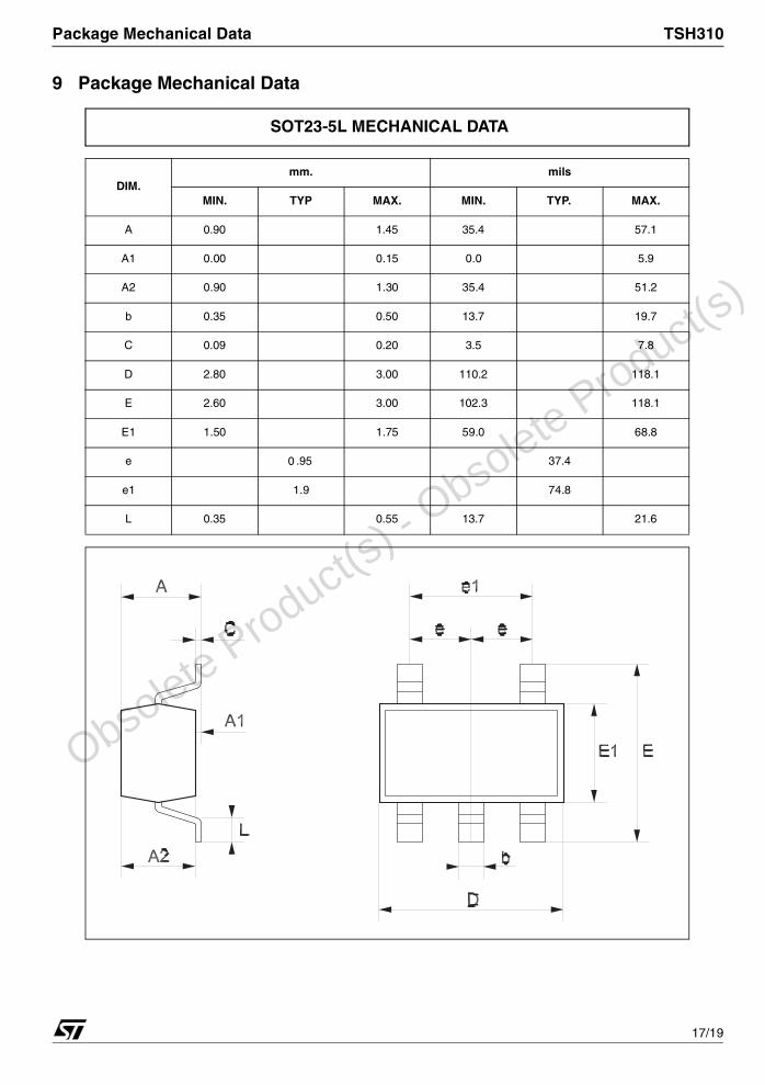
9 Package Mechanical Data
DIM.mm. mils
MIN. TYP MAX. MIN. TYP. MAX.
A 0.90 1.45 35.4 57.1
A1 0.00 0.15 0.0 5.9
A2 0.90 1.30 35.4 51.2
b 0.35 0.50 13.7 19.7
C 0.09 0.20 3.5 7.8
D 2.80 3.00 110.2 118.1
E 2.60 3.00 102.3 118.1
E1 1.50 1.75 59.0 68.8
e .95 37.4
e1 1.9 74.8
L 0.35 0.55 13.7 21.6
SOT23-5L MECHANICAL DATA
0
Obso
lete Product(s)
- Obso
lete Product(s)
17/19
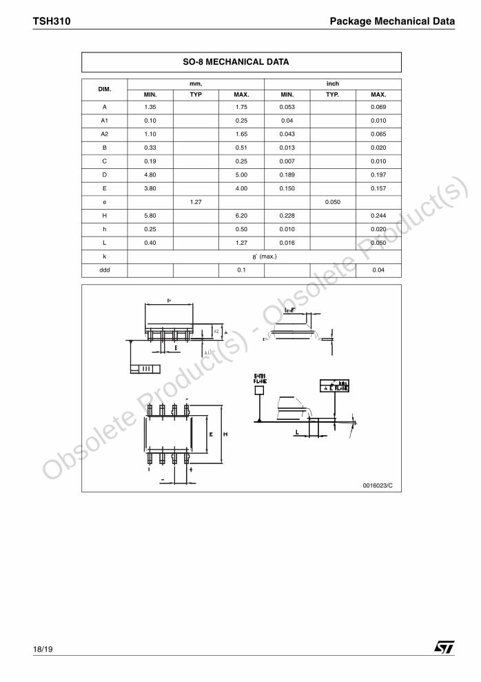
TSH310 Package Mechanical Data
DIM.mm. inch
MIN. TYP MAX. MIN. TYP. MAX.
A 1.35 1.75 0.053 0.069
A1 0.10 0.25 0.04 0.010
A2 1.10 1.65 0.043 0.065
B 0.33 0.51 0.013 0.020
C 0.19 0.25 0.007 0.010
D 4.80 5.00 0.189 0.197
E 3.80 4.00 0.150 0.157
e 1.27 0.050
H 5.80 6.20 0.228 0.244
h 0.25 0.50 0.010 0.020
L 0.40 1.27 0.016 0.050
k ˚ (max.)
ddd 0.1 0.04
SO-8 MECHANICAL DATA
0016023/C
8
Obso
lete Product(s)
- Obso
lete Product(s)
18/19
Revision History TSH310
10 Revision History
Date Revision Description of Changes
01 Oct 2004 1 First release corresponding to Preliminary Data version of datasheet.
December 2004 2 Release of mature product datasheet.
Obso
lete Product(s)
- Obso
lete Product(s)
19/19
Information furnished is believed to be accurate and reliable. However, STMicroelectronics assumes no responsibility for the consequencesof use of such information nor for any infringement of patents or other rights of third parties which may result from its use. No license is grantedby implication or otherwise under any patent or patent rights of STMicroelectronics. Specifications mentioned in this publication are subjectto change without notice. This publication supersedes and replaces all information previously supplied. STMicroelectronics products are notauthorized for use as critical components in life support devices or systems without express written approval of STMicroelectronics.
The ST logo is a registered trademark of STMicroelectronicsAll other names are the property of their respective owners
© 2004 STMicroelectronics - All rights reserved
STMicroelectronics group of companiesAustralia - Belgium - Brazil - Canada - China - Czech Repubic - Finland - France - Germany - Hong Kong - India - Israel - Italy - Japan -
Malaysia - Malta - Morocco - Singapore - Spain - Sweden - Switzerland - United Kingdom - United States of Americawww.st.com