Embed Size (px)
Citation preview
8/3/2019 2N3390 - Obsolete
http://slidepdf.com/reader/full/2n3390-obsolete 1/8
2 N 3 3 9 0
/ 2 N 3 3 9 1
/ 2 N 3 3 9 1 A / 2 N 3 3 9 2
/ 2 N 3 3 9 3
Discrete POWER & Signa l
Technologies
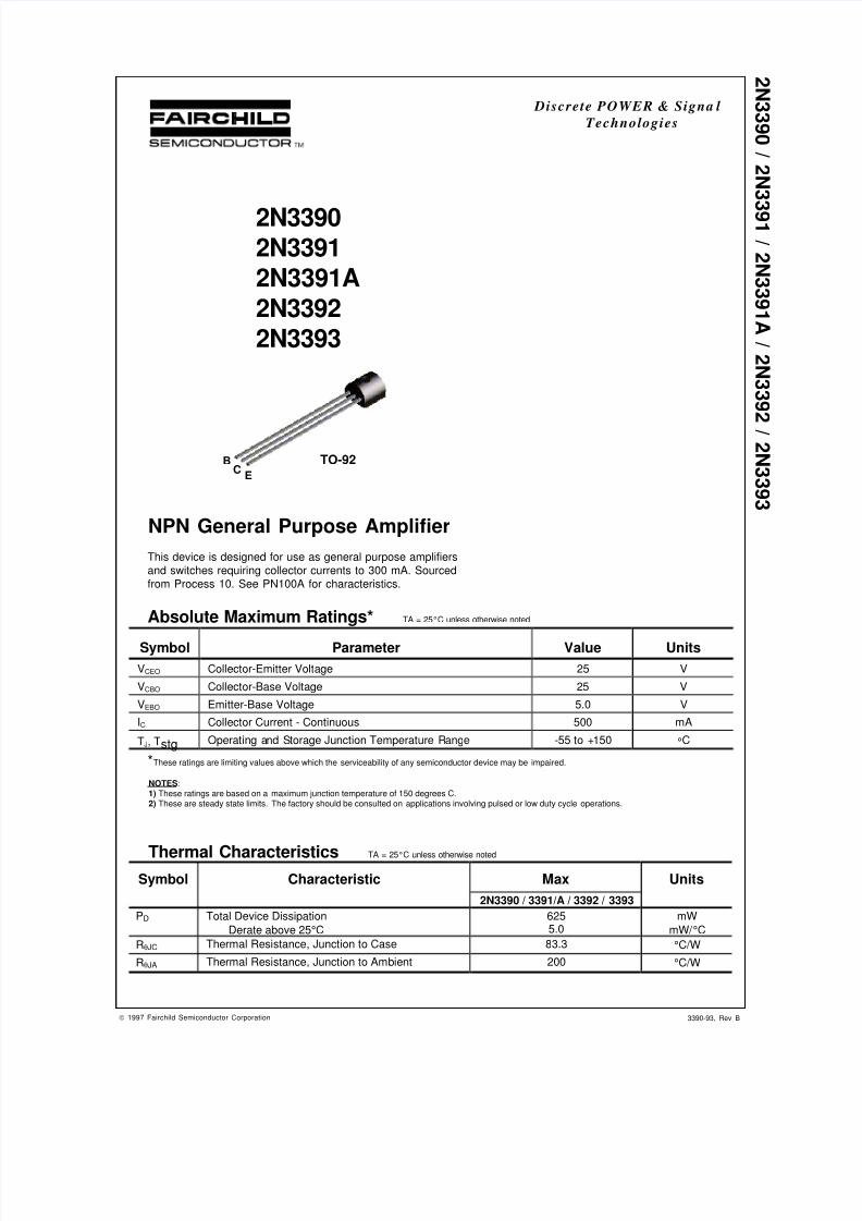
NPN General Purpose Amplifier
2N33902N33912N3391A
2N33922N3393
This device is designed for use as general purpose amplifiersand switches requiring collector currents to 300 mA. Sourcedfrom Process 10. See PN100A for characteristics.
Absolute Maximum Ratings* TA = 25°C unless otherwise noted
*These ratings are limiting values above which the serviceability of any semiconductor device may be impaired.
NOTES:1) These ratings are based on a maximum junction temperature of 150 degrees C.2) These are steady state limits. The factory should be consulted on applications involving pulsed or low duty cycle operations.
Thermal Characteristics TA = 25°C unless otherwise noted
Symbol Parameter Value Units
VCEO Collector-Emitter Voltage 25 V
VCBO Collector-Base Voltage 25 V
VEBO Emitter-Base Voltage 5.0 V
IC Collector Current - Continuous 500 mA
TJ, Tstg Operating and Storage Junction Temperature Range -55 to +150 °C
Symbol Characteristic Max Units
2N3390 / 3391/A / 3392 / 3393
PD Total Device Dissipation
Derate above 25°C
6255.0
mW
mW/ °C
RθJC Thermal Resistance, Junction to Case 83.3 °C/W
RθJA Thermal Resistance, Junction to Ambient 200 °C/W
BC
E
TO-92
© 1997 Fairchild Semiconductor Corporation 3390-93, Rev B
8/3/2019 2N3390 - Obsolete
http://slidepdf.com/reader/full/2n3390-obsolete 2/8
2 N 3 3 9 0
/ 2 N 3 3 9 1
/ 2 N 3 3 9 1 A / 2 N 3 3 9 2
/ 2 N 3 3 9 3
NPN General Purpose Amplifier(continued)
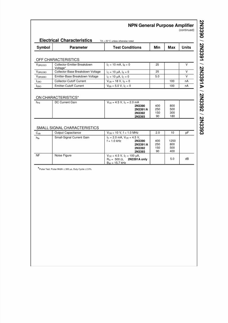
Electrical Characteristics TA = 25°C unless otherwise noted
OFF CHARACTERISTICS
Symbol Parameter Test Conditions Min Max Units
V(BR)CEO Collector-Emitter BreakdownVoltage*
IC = 10 mA, IB = 0 25 V
V(BR)CBO Collector-Base Breakdown Voltage IC = 10 µA, IE = 0 25 V
V(BR)EBO Emitter-Base Breakdown Voltage IE = 10 µA, IC = 0 5.0 V
ICBO Collector-Cutoff Current VCB = 18 V, IE = 0 100 nA
IEBO Emitter-Cutoff Current VEB = 5.0 V, IC = 0 100 nA
ON CHARACTERISTICS*
hFE DC Current Gain VCE = 4.5 V, IC = 2.0 mA2N33902N3391/A
2N33922N3393
400250
15090
800500
300180
SMALL SIGNAL CHARACTERISTICS
Cob Output Capacitance VCB = 10 V, f = 1.0 MHz 2.0 10 pF
hfe Small-Signal Current Gain IC = 2.0 mA, VCE = 4.5 V,f = 1.0 kHz 2N3390
2N3391/A2N33922N3393
40025015090
1250800500400
NF Noise Figure VCE = 4.5 V, IC = 100 µA,
RG = 500 Ω, 2N3391A onlyBW = 15.7 kHz
5.0 dB
*Pulse Test: Pulse Width ≤ 300 µs, Duty Cycle ≤ 2.0%
8/3/2019 2N3390 - Obsolete
http://slidepdf.com/reader/full/2n3390-obsolete 3/8
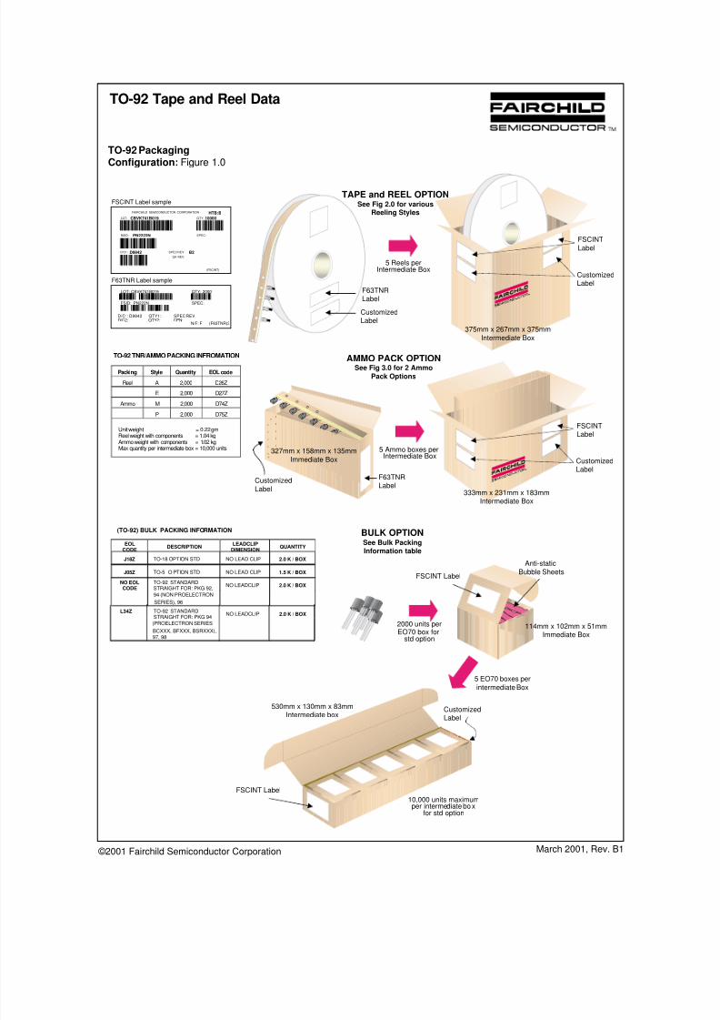
TO-92 Tape and Reel Data
March 2001, Rev. B1 ©2001 Fairchild Semiconductor Corporation
TO-92 PackagingConfiguration: Figure 1.0
AMMO PACK OPTIONSee Fig 3.0 for 2 Ammo
Pack Options
2000 units perEO70 box for
std option
FSCINT Label
530mm x 130mm x
83mm
Intermediate box
10,000 units maximumper
intermediate boxfor std option
FSCINT Label
114mm x 102mm x 51mmImmediate Box
Anti-static
Bubble Sheets
(TO-92) BULK PACKING INFORMATION
EOLCODE
DESCRIPTIONLEADCLIP
DIMENSIONQUANTITY
J18Z TO-18 OPTION STD NO LEAD CLIP 2.0 K / BOX
J05Z TO-5 O PTION STD NO LEAD CLIP 1.5 K / BOX
NO EOLCODE
TO-92 STANDARDSTRAIGHT FOR: PKG 92,
NO LEADCLIP 2.0 K / BOX
BULK OPTIONSee Bulk PackingInformation table
375mm x 267mm x 375mm
Intermediate Box
FSCINT
Label
CustomizedLabel
333mm x 231mm x 183mmIntermediate Box
FSCINTLabel
CustomizedLabel
TO-92 TNR/AMMO PACKING INFROMATION
Packing Style Quantity EOL code
Reel A 2,000 D26Z
E 2,000 D27Z
Ammo M 2,000 D74Z
P 2,000 D75Z
Unit weight = 0.22 gmReel weight with components = 1.04 kgAmmo weight with components = 1.02 kgMax quantity per intermediate box = 10,000 units
F63TNRLabel
5 Ammo boxes perIntermediate Box
Customized
Label
327mm x 158mm x 135mm
Immediate Box
LOT: CBVK741B019
NSID: PN2222N
D/C1: D9842 SPEC REV: B2
SPEC:
QTY: 10000
QA REV:
FAIRCHILD SEMICONDUCTOR CORPORATION HTB:B
(FSCINT)
F63TNRLabel
CustomizedLabel
5 Reels perIntermediate Box
TAPE and REEL OPTIONSee Fig 2.0 for various
Reeling Styles
LOT: CBVK741B019
FSID: PN222N
D/C1: D9842 QTY1: SPEC REV:
SPEC:
QTY: 2000
D/C2: QTY2: CPN:N/F: F (F63TNR)3
F63TNR Label sample
FSCINT Label sample
C
5 EO70 boxes per
intermediate Box
ustomizedLabel
94 (NON PROELECTRON
SERIES), 96
L34Z TO-92 STANDARDSTRAIGHT FOR: PKG 94
NO LEADCLIP 2.0 K / BOX
(PROELECTRON SERIES
BCXXX, BFXXX, BSRXXX),
97, 98
8/3/2019 2N3390 - Obsolete
http://slidepdf.com/reader/full/2n3390-obsolete 4/8
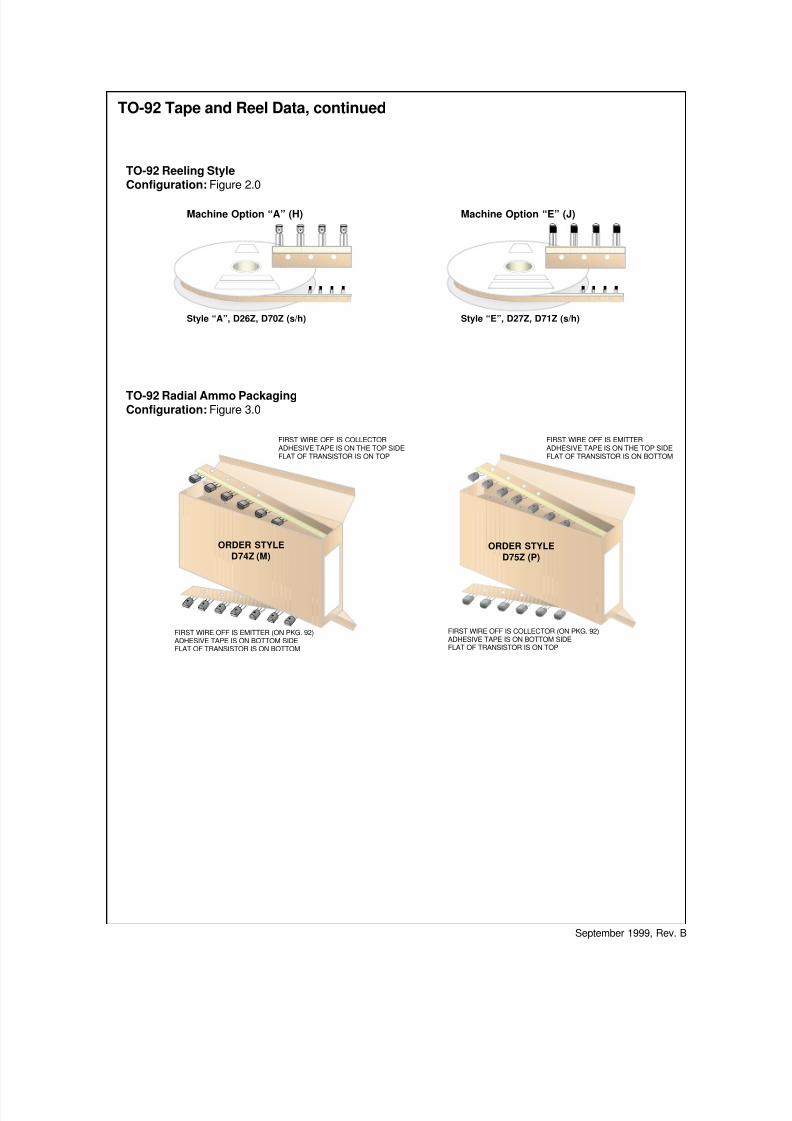
TO-92 Tape and Reel Data, continued
September 1999, Rev. B
TO-92 Reeling StyleConfiguration: Figure 2.0
Style “A”, D26Z, D70Z (s/h)
Machine Option “A” (H)
Style “E”, D27Z, D71Z (s/h)
Machine Option “E” (J)
FIRST WIRE OFF IS EMITTERADHESIVE TAPE IS ON THE TOP SIDEFLAT OF TRANSISTOR IS ON BOTTOM
ORDER STYLE
D75Z (P)
FIRST WIRE OFF IS COLLECTORADHESIVE TAPE IS ON THE TOP SIDEFLAT OF TRANSISTOR IS ON TOP
ORDER STYLE
D74Z (M)
TO-92 Radial Ammo PackagingConfiguration: Figure 3.0
FIRST WIRE OFF IS EMITTER (ON PKG. 92)ADHESIVE TAPE IS ON BOTTOM SIDEFLAT OF TRANSISTOR IS ON BOTTOM
FIRST WIRE OFF IS COLLECTOR (ON PKG. 92)ADHESIVE TAPE IS ON BOTTOM SIDEFLAT OF TRANSISTOR IS ON TOP
8/3/2019 2N3390 - Obsolete
http://slidepdf.com/reader/full/2n3390-obsolete 5/8
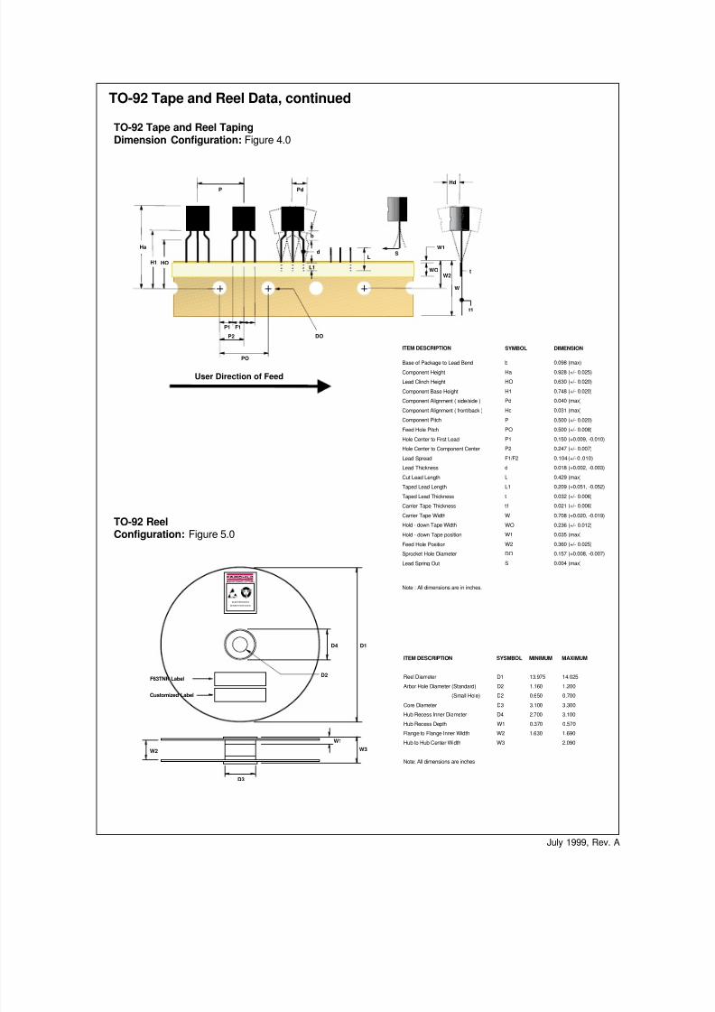
ITEM DESCRIPTION
Base of Package to Lead Bend
Component Height
Lead Clinch Height
Component Base Height
Component Alignment ( side/side )
Component Alignment ( front/back )
Component Pitch
Feed Hole Pitch
Hole Center to First Lead
Hole Center to Component Center
Lead Spread
Lead Thickness
Cut Lead Length
Taped Lead Length
Taped Lead Thickness
Carrier Tape Thickness
Carrier Tape Width
Hold - down Tape Width
Hold - down Tape position
Feed Hole Position
Sprocket Hole Diameter
Lead Spring Out
SYMBOL
b
Ha
HO
H1
Pd
Hd
P
PO
P1
P2
F1/F2
d
L
L1
t
t1
W
WO
W1
W2
DO
S
DIMENSION
0.098 (max)
0.928 (+/- 0.025)
0.630 (+/- 0.020)
0.748 (+/- 0.020)
0.040 (max)
0.031 (max)
0.500 (+/- 0.020)
0.500 (+/- 0.008)
0.150 (+0.009, -0.010)
0.247 (+/- 0.007)
0.104 (+/- 0 .010)
0.018 (+0.002, -0.003)
0.429 (max)
0.209 (+0.051, -0.052)
0.032 (+/- 0.006)
0.021 (+/- 0.006)
0.708 (+0.020, -0.019)
0.236 (+/- 0.012)
0.035 (max)
0.360 (+/- 0.025)
0.157 (+0.008, -0.007)
0.004 (max)
Note : All dimensions are in inches.
ITEM DESCRIPTION SYSMBOL MINIMUM MAXIMUM
Reel Diameter D1 13.975 14.025
Arbor Hole Diameter (Standard) D2 1.160 1.200
(Small Hole) D2 0.650 0.700
Core Diameter D3 3.100 3.300
Hub Recess Inner Diameter D4 2.700 3.100
Hub Recess Depth W1 0.370 0.570
Flange to Flange Inner Width W2 1.630 1.690
Hub to Hub Center Width W3 2.090
Note: All dimensions are inches
TO-92 Tape and Reel TapingDimension Configuration: Figure 4.0
Ha
H1 HO
PO
P2
P1 F1
DO
P Pd
b
d
L1
LS
WOW2
W
t
t1
Hd
W1
TO-92 Reel
Configuration: Figure 5.0
User Direction of Feed
SENSITIVEDEVICES
ELECTROSTATIC
D1
D3
Customized Label
W2
W1
W3
F63TNR Label
D4
D2
TO-92 Tape and Reel Data, continued
July 1999, Rev. A
8/3/2019 2N3390 - Obsolete
http://slidepdf.com/reader/full/2n3390-obsolete 6/8
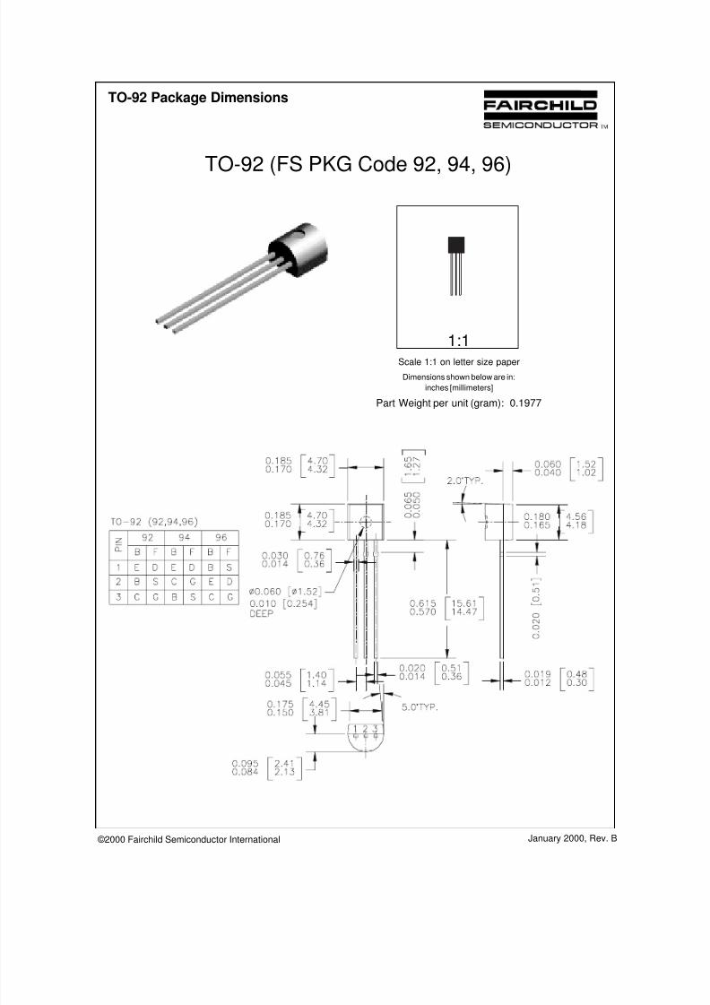
TO-92 (FS PKG Code 92, 94, 96)
TO-92 Package Dimensions
January 2000, Rev. B
1:1Scale 1:1 on letter size paper
Dimensions shown below are in:
inches [millimeters]
Part Weight per unit (gram): 0.1977
©2000 Fairchild Semiconductor International
8/3/2019 2N3390 - Obsolete
http://slidepdf.com/reader/full/2n3390-obsolete 7/8
TRADEMARKS
The following are registered and unregistered trademarks Fairchild Semiconductor owns or is authorized to use and isnot intended to be an exhaustive list of all such trademarks.
LIFE SUPPORT POLICY
FAIRCHILD’S PRODUCTS ARE NOT AUTHORIZED FOR USE AS CRITICAL COMPONENTS IN LIFE SUPPORTDEVICES OR SYSTEMS WITHOUT THE EXPRESS WRITTEN APPROVAL OF FAIRCHILD SEMICONDUCTOR CORPORATION.As used herein:
1. Life support devices or systems are devices orsystems which, (a) are intended for surgical implant intothe body, or (b) support or sustain life, or (c) whosefailure to perform when properly used in accordancewith instructions for use provided in the labeling, can bereasonably expected to result in significant injury to theuser.
2. A critical component is any component of a lifesupport device or system whose failure to perform canbe reasonably expected to cause the failure of the lifesupport device or system, or to affect its safety or
effectiveness.
PRODUCT STATUS DEFINITIONS
Definition of Terms
Datasheet Identification Product Status Definition
Advance Information
Preliminary
No Identification Needed
Obsolete
This datasheet contains the design specifications forproduct development. Specifications may change inany manner without notice.
This datasheet contains preliminary data, andsupplementary data will be published at a later date.Fairchild Semiconductor reserves the right to makechanges at any time without notice in order to improvedesign.
This datasheet contains final specifications. FairchildSemiconductor reserves the right to make changes atany time without notice in order to improve design.
This datasheet contains specifications on a productthat has been discontinued by Fairchild semiconductor.The datasheet is printed for reference information only.
Formative orIn Design
First Production
Full Production
Not In Production
DISCLAIMER
FAIRCHILD SEMICONDUCTOR RESERVES THE RIGHT TO MAKE CHANGES WITHOUT FURTHER
NOTICE TO ANY PRODUCTS HEREIN TO IMPROVE RELIABILITY, FUNCTION OR DESIGN. FAIRCHILD
DOES NOT ASSUME ANY LIABILITY ARISING OUT OF THE APPLICATION OR USE OF ANY PRODUCT
OR CIRCUIT DESCRIBED HEREIN; NEITHER DOES IT CONVEY ANY LICENSE UNDER ITS PATENTRIGHTS, NOR THE RIGHTS OF OTHERS.
PowerTrenchQFET™
QS™QT Optoelectronics™
Quiet Series™
SILENT SWITCHERSMART START™
SuperSOT™-3SuperSOT™-6SuperSOT™-8
FASTr™GlobalOptoisolator™
GTO™HiSeC™ISOPLANAR™
MICROWIRE™OPTOLOGIC™
OPTOPLANAR™PACMAN™POP™
Rev. G
ACEx™Bottomless™
CoolFET™CROSSVOLT ™DOME™
E2CMOSTM
EnSignaTM
FACT™
FACT Quiet Series™
FAST
SyncFET™TinyLogic™
UHC™VCX™

8/3/2019 2N3390 - Obsolete
http://slidepdf.com/reader/full/2n3390-obsolete 8/8
This datasheet has been download from:
www.datasheetcatalog.com
Datasheets for electronics components.