Embed Size (px)
Citation preview

Microfabrication Techniques for Accelerators
Symposium in Memory of Robert H. Siemann
and ICFA Mini-Workshop on Novel Concepts for Linear Accelerators and Colliders
A. Nassiri, R.L. Kustom, D.C. Mancini
Argonne National Laboratory

Microfabrication Techniques for AcceleratorsA. Nassiri Novel Concepts for LinearAccelerators and Colliders
2
Outline
TerminologyMicrofabrication methods and toolsDXRL at APSSummary

Microfabrication Techniques for AcceleratorsA. Nassiri Novel Concepts for LinearAccelerators and Colliders
3
Terminology and relative sizes
10-10m 10-9m 10-8m 10-7m 10-6m 10-5m 10-4m 10-2m10-3m 10-1m 1mAngstrom 1 nm 10 nm 100 nm 1 m 10 m 100 m 10 mm 100 mm1 mm 1000 mm
Log scale
Dimension
Atom Molecule Virus Bacteria Humanhair
Humantooth
Humanhand
Nanotechnology Microsystem technology Traditional eng. linear dimensions
Precision engineering
Examples of
objects
Terminology
Molecular engineeringFabricationmethods Silicon layer technologies
How toobserve X-ray techniques/STM Optical techniques Magnifying glass Naked eye
Nanofabrication technologies LIGA process
Precisionmachining
Conventional machining
Casting, forming, sheet-metalworking
Dalmatian(average length)

Microfabrication Techniques for AcceleratorsA. Nassiri Novel Concepts for LinearAccelerators and Colliders
4
Microfabrication methods and tools - MEMS
Basic idea is to find a way to circumvent the limitations imposed by normalmachining.MEMS (Micro-electrical-mechanical systems)– Fabricated at micron to millimeter sizes using a single silicon substrate– Used to fabricated sensors, motors, actuators, mirrors
• Wide range of industrial and consumer applications– MEMS accelerometers for automobile airbag systems– MVED applications
• MEMS-based reflex klystron (JPL)
A salient-pole electrostatic ally actuatedmicromotor made from polycrystalline siliconusing surface micromachining techniques.
A mechanical gear which is smallerthan a human hair

Microfabrication Techniques for AcceleratorsA. Nassiri Novel Concepts for LinearAccelerators and Colliders
5
MEMS fabrication processWet Etching– Isotropic wet etching uses solutions of hydrofluoric, nitric, and acetic acid,
HNA.– It produces hemispherical shaped cavities below the mask aperture.– Lateral etch rate is about the same as vertical etch rate– Anisotropic wet etching of silicon is done using either potassium hydroxide,
KOH, or a solution of ethylene diamine and pyrocatechol, EDPDry Etching– It provides a better control and faster etch rates than either isotropic or
anisotropic wet etching.– It refers to the process of reactive ion etching (RIE)
• Ionization of fluorine-rich reactive gas in a plasma chamber• Energetic fluorine ions attack the silicon surface
Mask
Scalloped edges
Substrate

Microfabrication Techniques for AcceleratorsA. Nassiri Novel Concepts for LinearAccelerators and Colliders
6
Microfabrication methods and tools – Laser Ablation
Laser ablation micromachining uses the very high power density and very shortpulse of the laser to vaporize the surface of a material without transferring heat tothe surrounding area.It can be applied to a a wide variety of materials including metals, ceramics,semiconductors and plastics.– The depth of the etch can only be done by knowing the material removal rate
per pulse and counting pulses or by external measurement.
a) Pre-ablation
b) After ablation with one pulse
c) After ablation with 10 pulses
SEM images of an MgB2 ablated at 193 nm @12 J/cm2

Microfabrication Techniques for AcceleratorsA. Nassiri Novel Concepts for LinearAccelerators and Colliders
7
Microfabrication methods and tools – EDMElectric Discharge Machining uses large electric field arcs across the gap betweenthe two metal surfaces.The arc raises the local surface temperature to between 8,000C and 12,000C andmelts a roughly hemispherical volume on both the electrode and the work piece.Since the surface is formed by millions of small craters, it has a very poor surfacefinish.This can be improved considerably with finishing cuts, smaller wire diameter, lowerelectric fields.It needs additional treatment for low RF loss applications.Dimensional accuracy for EDM is roughly the same as precision machining.EDM gains in accuracy from its noncontact material removal, compared to normalmachining.Disadvantage: variation in height of the crater-defined surface.New wire-handling and tensioning systems have allowed EDM wire diameters to ~20 m ( as compared to 0.3 mm – 0.03 mm), EDM.
Slide courtesy: MicroBridge Services, Ltd

Microfabrication Techniques for AcceleratorsA. Nassiri Novel Concepts for LinearAccelerators and Colliders
8
Microfabrication methods and tools – LIGA
LIGA is a process in IC fabrication which involves lithography, electroplating, andmolding on a given substrate. (Lithographie, Galvanoformung und Abformug)LIGA allows structures to have heights of over 100 m with respect to the lateralsize.LIGA fabricates High Aspect Ratio Structures (HARMS).The ratio between the height and the lateral size is the aspect ratio (e.g. 100:1)Ideal for fabrication of RF resonant cavities with frequencies from 30 GHz to 1THz.Unlike semiconductor lithography, LIGA uses very thick resist films.

Microfabrication Techniques for AcceleratorsA. Nassiri Novel Concepts for LinearAccelerators and Colliders
9
Deep X-ray Lithography and Electroforming
Copper
Silicon wafer, 250- m-thickGold absorber, 45-60- m-thickPMMA, 1 -3-mm-thickCopper base, 50-mm-thickCopper plating
Substrate
Resist
X-Rays
X-Ray Mask
SU-8 LIGA– An alternative to PMMA– For X-ray LIGA applications, it has a significant
advantage:• About 200 times more sensitive to X rays than
PMMA• This drops exposure times by two orders of
magnitude.• Disadvantage: The etchants that attack the
exposed SU-8 also attack the metal surface of theLIGA part.
Substrate
Substrate
Substrate
Substrate

Microfabrication Techniques for AcceleratorsA. Nassiri Novel Concepts for LinearAccelerators and Colliders
10
X-ray Exposure Station at the Advanced Photon Source ofArgonne National Laboratory
X-ray beam outlet
Scanner
APS Lithography beamline:
19.5 keV
Highly collimated beam ( < 0.1 mrad)
Beam size @exposure station: 100 (H) x 5 (v) mm2
Using a high-speed scanner ( 100 mm/sec) for uniform exposure.
Precision angular (~0.1 mrad) and positional (<1 micron) control ofthe sample.
exposure time:
1-mm thick PMMA ( 100 x 25 mm2) ~1/2 hr
10-mm thick PMMA ~ 2-3 hrs

Microfabrication Techniques for AcceleratorsA. Nassiri Novel Concepts for LinearAccelerators and Colliders
11
Antiscatter Grid for Mammography
Freestanding focused to the point copper antiscatter grid 60 mm x 60 mm in sizewith 25-µm-wide septa walls and 550 µm period and 2.8 mm tall (grid ratio 5.3).
Detail of x-ray mask used forobtaining freestanding copperantiscatter grid
Scatter– Produces slowly varying background fog– Reduces subject contrast– Reduces the ability to identify diseased tissues
Microfabrication Techniques for AcceleratorsA. Nassiri Novel Concepts for LinearAccelerators and Colliders
12
Unique benefits of ANL
APS is one of the very few light sources worldwide suitable formicromechanics with a unique possibility of dynamic exposure forvery tall (1-3mm) structures.
Knowledgeable and experienced staff provides excellent usersupport.
X-ray lithography station in Sector 10 is fully operational on a sharedbend magnet beamline.
Long experience in fabricating copper high-aspect ratiomicrostructures.

Microfabrication Techniques for AcceleratorsA. Nassiri Novel Concepts for LinearAccelerators and Colliders
13
3-D Conceptual Planar Structure
CoolantCoolantBeam AxisBeam Axis
Vacuum + HOMVacuum + HOM
Alignment Slots &Alignment Slots &Bonding FibersBonding Fibers
CoolantCoolant
RF InputRF Input
VacuumVacuum
CoolingCooling
Lower half of a Side-coupled planar SWStructure
Lower half of an on-axis planar SWstructure

Microfabrication Techniques for AcceleratorsA. Nassiri Novel Concepts for LinearAccelerators and Colliders
14
PMMA Masks with DXRL: 94 GHz CG 1
Long structure (66 cells)
Short structure (30 cells)
Magnification40X
Magnification40X
1 J. Song, at al., Proc. Particle Accel Conf., Vancouver, B.C., Canada, 1997

Microfabrication Techniques for AcceleratorsA. Nassiri Novel Concepts for LinearAccelerators and Colliders
15
Constant impedance cavity1
High aspect ratioSurface roughness <50 nmHigh accuracy < 1 m
SEM image of 108-GHz CI structure.
1 A. Nassiri, at al., Proc. Int. Electron Devices Meeting, Washington, DC, December1993
Muffin-tin cavity RF parameters
Frequency f 120 GHz
Shunt impedance R0 312 M /m
Quality factor Q 2160
Operating mode TW 2 /3
Group velocity g 0.043c
Attenuation 13.5 m-1
Accel. Gradient E 10 MV/m
Peak power P 30 kW

Microfabrication Techniques for AcceleratorsA. Nassiri Novel Concepts for LinearAccelerators and Colliders
16
Multi-beam Planar Klystron1
Output WaveguideOutput Waveguide
CavitiesCavities
CollectorCollector
AnodeAnodeInput WaveguideInput Waveguide
CathodeCathodeInsulatorInsulator
InsulatorInsulator
BeamBeam
CollectorCollectorCavitiesCavities
BeamBeam
OutputOutputWaveguideWaveguide
InputInputWaveguideWaveguide
1 Y. W. Kang (ORNL/SNS): private communication

Microfabrication Techniques for AcceleratorsA. Nassiri Novel Concepts for LinearAccelerators and Colliders
17
Accelerator on a Substrate
CollectorCollector
LoadLoad
DirectionalDirectionalCouplerCoupler
CirculatorCirculator
Output Waveguide CavityOutput Waveguide Cavity
GunGun
DirectionalDirectionalCouplerCoupler
DirectionalDirectionalCouplerCoupler
Input Waveguide CavityInput Waveguide Cavity
Accelerating StructureAccelerating Structure
MU
LTIB
EAM
PLA
NA
R K
LYST
RO
NM
ULT
IBEA
M P
LAN
AR
KLY
STR
ON
VacuumVacuumTankTank

Microfabrication Techniques for AcceleratorsA. Nassiri Novel Concepts for LinearAccelerators and Colliders
18
Comparison of Microfabrication Methods for RF Structures
Each fabrication method discussed has specific advantages for different materialsand geometries.Normal machining can produce RF structures up to several hundred gigahertz aslong as surface finish and consequent surface losses are not important.In resonant structures where surface losses drastically degrade the performance,normal machining is limited to less than 100-GHz structures.EDM has similar issues regarding surface losses– Can handle hard-to-machine materials. Only conductive materials
LIGA is effective in a range of frequency defined by– Depth to which the photoresist can be exposed
• 6-mm thick PMMA “routine”• 10-mm thick PMMA soon
– Dimensional accuracy limits of the mask and the diffraction of the light source.• Smallest lateral size is 0.2 m.• Aspect ratios can range up to 500.• Surface roughness is small (~30 nm).
f 25 GHz

Microfabrication Techniques for AcceleratorsA. Nassiri Novel Concepts for LinearAccelerators and Colliders
19
Characteristics of Microfabrication Methods
DimensionalAccuracy( m)
SurfaceFinish(nm)
CompatibleMaterials
Litho or SerialProcess
Cost per Part FrequencyRange(GHz)
LIGA PMMA ±1 < 200 Metals Litho Low 25 - 600
LIGA SU-8 ±1 < 200 Metals Litho Low 25 - 600
MEMS(WE) ±0.5 < 50 Silicon Litho Low 300-3000
MEMS (DRIE) ±0.5 < 50 Silicon Litho Low 300-3000
Laser ablation ±2 200-500 Almost any Litho/Serial High 100-300
materials
EDM ±2 <1000 Conductors Serial High 0-300
Normal machining ±8 <1000 Almost any Serial Medium/High 0-100
materials

Microfabrication Techniques for AcceleratorsA. Nassiri Novel Concepts for LinearAccelerators and Colliders
20
Can a “true” 3D structure be realized?As attractive DXRL is, it can only fabricate microstructures with vertical wall,which limits their application.Although 3D structures can be realized by various LIGA techniques, structureshave walls parallel to the incident X-ray.To overcome these limitations with the conventional lithography techniques, Tworecently new techniques have been developed:– A moving mask deep X-ray lithography (M2DXL)1.
• M2DXL is a technique to fabricate microstructures with controllable inclinedor curve wall.
– A double X-ray exposure technique2
• 3D is realized by controlling the propagation direction of the PMMAdissolution front. This is achieved by irradiating the whole PMMA surfaceagain without the X-ray mask after the first exposure.
1 Y. Hirai, et. al, J. Micromech. 17 (2007)2 N. Matsuzuka, et. al, 17th IEEE MEMS, 2004
3D microstructure fabricated by moving mask UVlithography techniques.
Microfabrication Techniques for AcceleratorsA. Nassiri Novel Concepts for LinearAccelerators and Colliders
21
SummaryTechnology for a fully integrated design in not (yet) available and not likely in thenear future.Hybrid design, ala hybrid integrated-electronic circuits, is closer to being available,requires considerable R&D.Fabrication challenges of RF structures and circuits– Vacuum-sealing and vacuum pumping of circuit with sub-millimeter beam
apertures– RF losses due to surface roughness
• = 200 nm @95 GHZ and 66 nm@1THz for copper• Need surface roughness less that the skin depth
– Dimensional accuracy of cavities/circuits and alignment• Dimensional accuracy required 1/BW
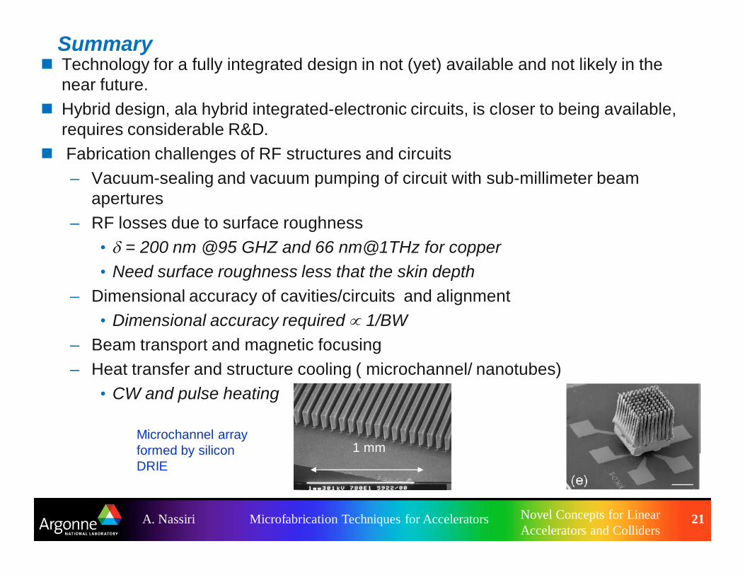
– Beam transport and magnetic focusing– Heat transfer and structure cooling ( microchannel/ nanotubes)
• CW and pulse heating
Microchannel arrayformed by siliconDRIE
1 mm

Microfabrication Techniques for AcceleratorsA. Nassiri Novel Concepts for LinearAccelerators and Colliders
22
Thank you.


![Omega Kustom Manual [final] - Speedway Motors · Omega Kustom Manual [final].cdr Author: Rebecca Doremus Created Date: 10/14/2009 12:27:42 AM](https://img.pdfslide.us/doc/110x75/5f6e9f4f4c8fe342650d99ff/omega-kustom-manual-final-speedway-motors-omega-kustom-manual-finalcdr-author.jpg)