Embed Size (px)
Citation preview
NATIONAL INSTITUTE OF OCEANOGRAPHY
WORMLEY, GODALMiNG, SURREY
A Multiple Floating-d.c. Power Supply
for an Analogue Computer
by
S. ISHIGURO AND A. J. BUNTING
N . I . O . INTERNAL REPORT N O . A . 3 5
JULY 1968
mTIONAL INSTITUTE 0? OCEANOGRAPHY
Wonnley, Godalming^ Surrqy.
A Multiple Floating-d.o. Power Supply for an Analogue Computer
by
S. Ishiguro and A.J. Bunting
N.I.O. Internal Report No. A.35.
July 1
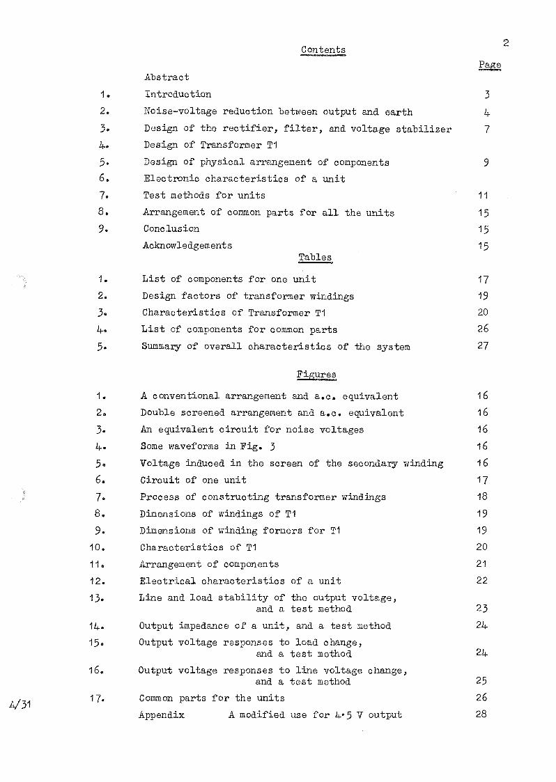
Contents
2. 3.
k'
5.
6. 7.
8. 9.
1. 2. 3.
Abstract
Introduction
iWoise-Toltage reduotion between output and earth
Design of the rectifier, filter, and voltage stabilizer
Design of Transformer T1
Design of physical arrangement of components
Electronic characteristics of a unit
Test methods for units
Arrangement of common parts for all the units
Conclusion
Acknowledgements Tables
List of components for one unit
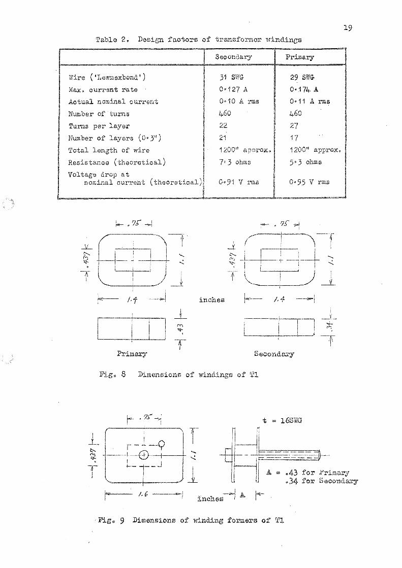
Design factors of transformer windings
Characteristics of Transformer T1
List of components for common parts
Summary of overall characteristics of the system
3
4
7
11
15
15
15
17
19
20
26
27
Piaures
1. A conventional arrangement and a.c. equivalent 16
2. Double screened arrangement and a.c. equivalent 16
3. An equivalent circuit for noise voltages 16
4. Some waveforms in Pig. 3 16
5» Voltage induced in the screen of the secondary winding 16
6 . Circuit of one unit 17
7» Process of constructing transformer windings 18
8. Dimensions of windings of T1 19
9. Dimensions of winding formers for T1 19
10. Characteristics of T1 20
11. Arrangement of components 21
12. Electrical characteristics of a unit 22
13. Line and load stability of the output voltage,
and a test method 23
14. Output impedance of a unit, and a test method 24
15« Output voltage responses to load change, and a test method 24
16. Output voltage responses to line voltage change,
and a teat method 2$
17. Common parts for the units 26
Appendix A modified use for 4*5 V output 28
Abstraot
Some types of electronic analogue computer require a multiple floating power supply having d.c. outputs whose electrical isolation from each kther, from the circuit earth, and other parts can be regarded as perfect with respect to the analogy. Since such a power supply operated from a power line is not commercially available so far, this has been Aveloped for the purpose. Noise voltage both between output terminals and between output terminals and earth is less than 200 pV p-p. Each output is 10*00 V with a stability of < ± 0»03^ against line voltage (± 10^), and load current (O to 60 mA), and a temperature stability of 0*01^ per C. The output impedance is less than 0«05 ohm from d.c. to 10 kHz. A short-circuit protection and remote-error-voltage-sensing terminals have been prepared for each unit. The number of output units is unlimited in principle, with a flexibility in electrical and physical arrangement. The cost of the power supply is comparable to that of battery operations.
1. Introduction
An electronic analogue model, designed by Ishiguro at the
National Institute of Oceanography for analysing storm surges in
the North Sea, has been operated suooessfully s&yeral ye&rs, * This
consists of a number of transistor circuits whose power supplies cannot
be common and should be isolated electrically from earth. These are
operated at the moment by individual dry batteries for simplicity of
arrangement, although these have several disadvantages such as
relatively high output impedance, voltage changes with time, and
necessity of quite frequent replacements.
A power supply for this application should satisfy the following
conditions at least:
(1) The input power should be supplied from a 2W3 V rms i 10^^ $0 Hz ± 1%
line, and the d.c. output should be divided into a considerable number of
units, say 200, The cost per unit should be reasonable compared with that
of the main part of the apparatus,
(2) The d.c. outputs should be isolated electrically from each other,
from the power line and from earth, with a high impedance, say >100 M ohms.
However, a small capacity, say <$00 pF with a stability of ± 1^^ can be
permitted between each d.c. output and earth, if the capacitance is
uniform throughout all the units.
(3) Noise voltage, including a.c. components, between each d.c.
output and earth should be small, say <0"5 mV p-p.
(4) Each d.c. output voltage should be highly stable, say ± 0*05^,
against changes of the line voltage (± 10^), frequency (l 1^), load
current (O to 60 mA), and nonnal environmental temperature change
(0° to +Zi.0°0). Ncise voltage, including a.c. components, contained
in each d.c. output should be small, say 0»5 mV p-p.
4
(5) The impeclanoe of each d.c. output should be lew, say 0*0$ ohm,
from d.o, to 10 kHz.
(6) Other items usually roquired for precision power supplies such as fast
recovery tine and snail over-shoot voltage, short warm-up time, short-circuit
protection, and remote-error-sensing terminals, are also preferable.
No commeroial product which satisfies all the conditions above is available
so far; only one commercial type satisfies Condition (3) but does not satisfy
Condition (l). Therefore, we have decided to develope a power supply
especially for this purpose.
The ains of tho design are as follows: (A) A principle which
requires a zininun of non-standard components has been chosen. (B) The
electronio circuit and its physical construction have been designed to be
as simple as possible, and to have optimum performance. ( c ) All the
components have been selected, from inexpensive versions due to mass
production and not duo to low quality, (d) In order to minimize costs no
special efforts have been mad.8 to miniaturize the equipment.
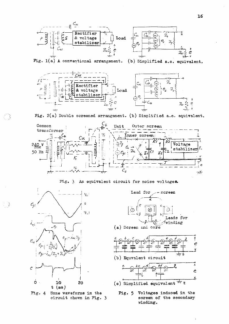
2. Noise-voltage reduction between outputs and earth
To satisfy Conditions (2) and (3) at the same time is the most important
requirement for this apparatus, and careful consideration is necessary.
Fig. 1 shows a conventional arrangenent of typical a.c. operated d.o*
power supply, with its a.c. equivalent. For conventional uses, one of the
d.c« output terminals is earthed so that = zero and e = zero. The
impedance between Terminals 1 and 2 is usually very low so that Terminal 2
is also practically earthed. Therefore no problem arises with respect to
Condition (3), even with large stray capacitances C and C_ existing. pS ILS
However, if is large as specified by Condition (2), both the primary and
secondary voltages appear, through these capacitances, between the output
terminals and earth. This is the main reason why conventional power supplies
cannot be applied for our purpose.
Fig. 2 shows one of the arrangements by which a conventional power
supply system can be applied to our purpose with minor alterations. In this
arrangement, a double screening is usod for the secondary winding and its
related parts, in addition to a separate screening for the primary winding.
The inner screen of the secondary part is connected to one of the d.o. output
terminals, while the rest of the screens are earthed® As shown in a simplified
a.c. equivalent circuit, e can be very small if C and are very small which
is not difficult to realise, C„. is now the only problem to solve. There
are two possible solutions: to make small so that for example
l/wC™ = 0'01 Z„., or to make C_. relatively small and stable as specified jhi I
by Condition (2).
A/31
The arrangement described in Fig. 2 can eliminate the main part
of the noiae voltage appearing between the d.c. output terminals and earth, _5
and this arrangement can reduoe the noise voltage to about 10 of the
primary voltage (700 Y p-p approximately if this is connected directly
to a power line). In order to reduce the noise voltage further,
other kinds of noise sources should be eliminated.
Noise voltages of 50 Hz component Since C (in Fig. 2) cannot be
zero, a part of line voltage is introduaed to the secondary
oirouit. In order to reduoe this effeot and to make thsseconday lead
wires as short as possible, two kinds of transformers are used between
the power line and the rectifier of each unit. The first transformer
TO is used in common for a group of units (say $0), and this steps down
the line voltage to about 20 V rms. This voltage is supplied ta an
isolating transformer T1 contained in each unit as shown in Fig. 3»
The primary circuit of T1 is earthed through an adjustable potentiometer
VE so that all 50 Hz component voltages appearing on the d*o. output,
through C , C,, C , C and r are cancelled; where C , C., C are ° a b c so 8 a b c
leakage capacitances due to the imperfection of the screens, is
the capacitance between the primary circuit of T1 and its screen, r is
the resistance of lead wires, and r is the resistance between the two e
earth points.
Noise voltage generated in the rectifier circuit Fig. 4 shows voltage
and current waveforms in the rectifier circuit (see Fig. 3 for symbols).
Since is kept almost constant all the time, the rectifier current i^^
can flow only when the secondary voltage of T1, e , becomes higher than
E. so that i takes a square-pulse like waveform. At the start of each 1 as
pulse, voltages rise with a relatively large time constant since the
circuit is loaded® At the end of each pulse, voltages fall with a very
small time constant since there is practically no load. This gives a
voltage wavefoim as shown e ^ in Fig. This voltage contains many
high frequency components as well as 50 Hz.
ttm rectified voltagehas passed the filter consisting of
Cg, it has almost only a 100 ]%z componeat with amplitudes of
600 mV p*^ across 0^, and 20 mV p-p across Cp .
These voltages and voltage e described previously appear between
the d.c. output and earth, even if the impedance between the output
terminals is zero, laolesa electrostatic coupling between these
parts and earth is eliminated. Therefore, all these parts should be
contained within the Inner screen. Imperfection of the inner screen
which is i-epresented by in Fig. 3 will produce a noise voltage* hut low
frequency components such as 50 and. 100 Hz are attenuated, more effectively
than high frequency components since is very small, so that the residual
noise voltage becomes a wavefora such as shown by e in Fig. 4-. This voltage
will be less than 0'2 mV p-p if the screens are arranged carefully.
Noise voltage due to resistance in conductors Several electronic ocmponents
of the secondary circuit are connected to a common conductor shown by a
thick line in Pig. 3. It can be regarded, for most cases, that such a
conductor has a uniform electric potential everywhere. Compared with
the no is e-voltage level specified for this power supply, however, irregularity
in voltage distribution on the conductor is appreciable. For example, a
GUI-rent of 100 mA p-p through a conductor which has resistance of 0'01 ohm
produces 1 mV p-p. In partioiilar a part of the conductor by which the
filter current is carried produces a considerable voltage containing 100 Hz
and high frequency components. If physical positions of electronic
components on the conductor are not correct such a voltage would appear
between -Qie d.c. output terminals and between the terminals and earth.
The worst arrangement is that the output terminal is connected near the
lead wire of and at the same time the error-voltage sensing circuit is
connected to the further end of the conductor. The best arrangement is
to-connect the components, including the inner screen, to the conductor in
the same order as shoim in Fig. 3.
Noise voltages due to ma^ietio coupling from T1 Conductors, such as screen
and lead wires, in the magnetic field of Transformer T1 produce voltages
depending on both the primaiy and secondary currents of the transformer
and conditions of couplingo For example, one turn of conductor around
the full flux will produce approximately 50 mV p-p of 50 Hz component
from the primary, and approximateHy 100 mV p-p of pulsed voltage from the
secondary, if the conductor has no load.
The electro-static screen for the secondaiy winding has the most
serious effect, since this has a complete turn around the full magnetio
fluz and is electrically is^/lated from earth. Fig. 5(8.) shows the geometric
relationship of the screen and the core. Fig. 5(b) shows an equivalent
circuit of electromotive force induced in the screen and its stray capacitance.
The stray capacitance per unit surface-area of the screen at and ^ is
approximately twice that of the rest of the screen, while the electromotive
force is distributed along the screen. Fig. 5(o) shows a simplified
equivalent of the previous circuit. When the two ends of a and b are kept
open, almost no voltage will appear between d and E, since the currents
V31
7
passing through the main stray capacitances cancel each other.
Therefore, d is the best position to connect the lead wire of the
screen I ah and fg are the worst areas to do so since induced
voltages will appear directly between the d.c. output and earth.
The lead wires of the secondary winding of T1 should also be screened,
and the end of the screen should be kept open.
The screen of the primary winding of T1 has the same effect, but
induced voltages do not appear between the output terminals and earth,
even if the lead wire is connected to any position, since the screen is
earthed.
The rest of the components should be arranged as far from the magnetic
flux as possible, although the. coupling effect on them is relatively small.
It should be noted that a magnetic screening would not be worth applying
since this has no effect on the electrostatic screen of the secondary
winding.
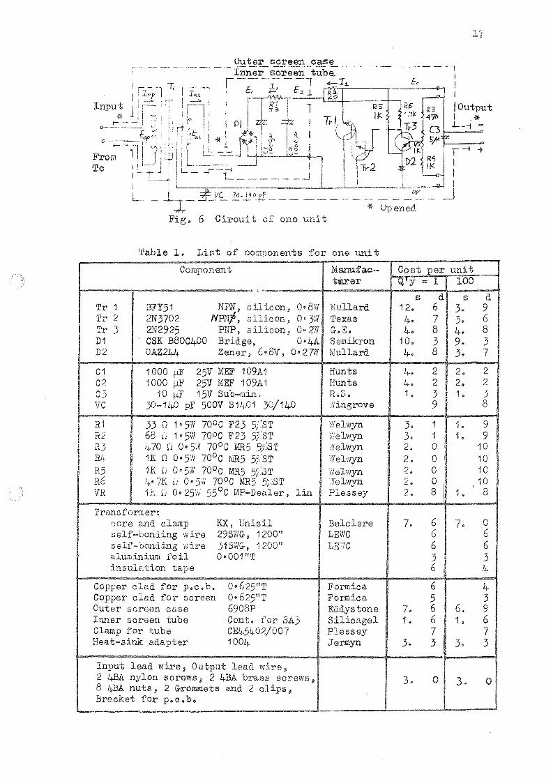
3» Design of the rectifier, filter, and voltage stabilizer
The circuit of one unit is shown in Fig. 6. Components for one
unit are listed in Table 1. A shiont-impedance voltage-regulator has
been employed since the total power dissipation of this apparatus is
not large and no special components are required for short circuit
protection. A bridge-connected silicon rectifier has been chosen
mainly from an aspect of physical size because this has to be contained
in the inner screen, A simple ripple filter, consisting of two 1000
capacitors and one 33 0 resistor, is used by which the ripple voltage
can be reduced to 20 mV p-p approximately. Their physical dimensions
are again an important factor in choice since they are also contained in
the inner screen. A large current rating resistor is used for R3 as well
as R2, since these act as the main heat dissipaters when a short circuit
is made between the output terminals. A combination of a PNP silicon
transistor and a silicon zener diode (E = 6*5 V at = 5 mA) has been
chosen for the error-voltage sensing circuit so that the combined
temperature coefficient becomes very small, A zener diode which has a
lower voltage will improve this combined coefficient, but it has a higher
dynamic aenea*impedance so that the voltage stability against current is
reduced. Therefore a comprcnised design has been nade for this point.
In order to operate the zener diode at a low dynamic zener-impedance by
increasing the average zener current, R5 is connected in series to the
zener diode from a stabilized voltage. Two NPN silicon transistors,
Tr-1 and Tr-2, are used for the main voltage controller and its amplifier.
It has been found that the circuit has a reasonable stability even without
Tr-2; but it is not sufficient to obtain a low impedance specified for
this apparatus. All the transistors have been chosen from the aspect of
low cost subject to these satisfying the technical requirements of the
circuit. The chosen types have much higher qucilities than required; the
main reason seems to be a mass production of these types due to a large
demand. Stctility and output inpodance for high-frequency load'ckanges
are limited only by strAgr oapacitonoes and inductances of other
components. In order to preserve a good frequency characteristic, therefore,
a capacitor is used to shunt the output terminals only for preventing a
self oscillation of the circuit. In order to make the capacitance between
the output and earth uniform throughout all the units, a preset capacitor
CV is used which can be adjusted from the outside of the case after each
unit :i.8 fixed to the computer. A pair of terminals for remote error-
voltage sensing is prepared inside the case. For this purpose a four-
conductor screened cable should be used. If this is not necessary, a twin-
conductor screened cable can be connected so that each error-sensing teiminal
and one of the output terminals are connected with a part of the conductor
respectively.
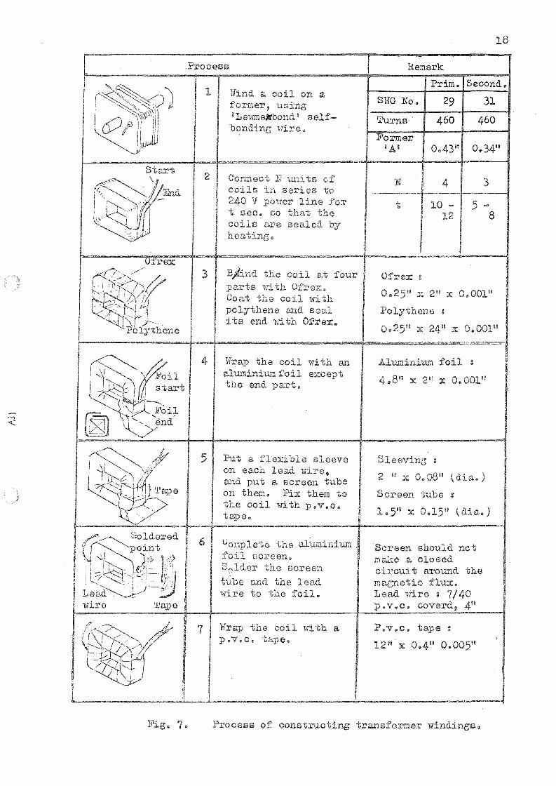
4. Design of Transformer
The electronic circuit shown in Fig. 6 requires $0 Hz 16 V rns,
100 mA to operate at the input terminals of the rectifier. The output
voltage of the mains transformer, TO, is 21*5 V rms. Transformer T1
should satisfy these conditions to connect these two parts, as well as
conditions required for screening of windings. From the power rating
required and the physical dimensions for screening, a Belclere Type KZ
Unisil core has been chosen. Design factors of the transformer windings
are shown in Table 2. This design wculd be flexible for changes of
voltages and current rating f abcu
Screening of the transformer is most important for this application.
Several methods of construction of screens have been examined; for example,
a metal plated bobbin with a metal-foil side-cover. The most successful
method is screening of each winding with a single metal foil without bobbins.
The process of constructing windings in such a way is shown in Fig. 7« The
dimensions of the primaiy and secondary windings are shown in Fig. 8. The
dimensions of winding formers are shown in Fig. 9.
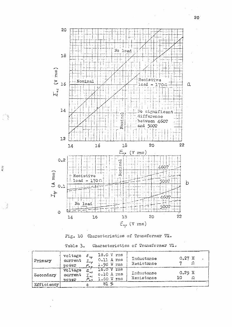
Some characteristics of a prototype transformer are shown in Fig. 10
and a sumary of the oharaotea-istics is shown in Table 3.
V31
5» Design of physical arrangement of components
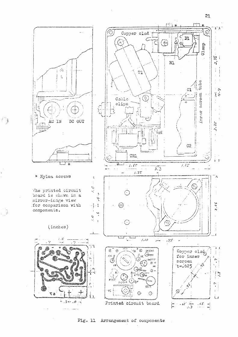
Arrangement of components for one unit is shown in Fig. 11.
A standard type aluminium-alloy die oast box with a lid has been
chosen for the case which, at the same time, acts as a heat sink,
electro-static screen and dust cover as well as a mounting chassis
for components. This has been found tho nost ooonoaioal way ao
far, although the size and weight of the case are somewhat too large
for this purpose. An aluminium container (originally designed for
a desiccator container) is used for the inner screen for the same
reason. This is fixed on the inside wall of the case with a metal
clamp (originally designed for a large cylindrical capacitor) and
two nylon screws by inserting an insulation plate with one surface
copper clad (originally designed as printed circuit board). The
copper cladding becomes the lid of the inner screen tube and has the
effect of screening. The transformer is also fixed inside the case
directly, with the input and output lead wires. The rest of the
electronic components are mounted on a printed circuit board which is
also fixed inside the case. The power transistor Tr-1 is held in
thermal contact with the case wall by an electrically insulated heat-
sink adaptor with a nylon screw. Two holes have been made for
adjusting VR and CR from outside the case, after each unit is
installed.
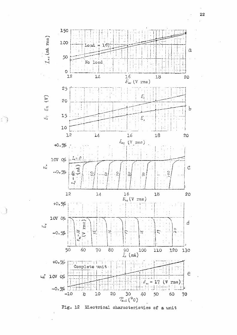
6, Electrical characteristics of a unit
Some electrical characteristics of a prototype unit have been
tested which has been designed according to the circuit shown in
Fig. 6 and the physical arrangement shown in Fig. 11.
Fig. 12(a) shows changes of a.c. input current, 3^^/ and voltage,
E , at the input of the rectofier with and without an external load
on the unit. The impedance at the nominal value of E = 17 V m s is as
approximately 170 ohms and is practically constant against the change
of load.
Fig. 12(b) shows d.c. voltages across and Cg, and Eg
respectively, against E . At the nominal value of E , E. = 19 V as as 1
and E_ = I6 V aoDroximately. E should not be higher than 20 V rms 6 - as
for the protection of CI whose working voltage is 2$ V.
Fig. 12(c) shows changes of d.c. output voltage E , as the
parameter of E^ , against the output current 1^. For the specified
maximum current of = 60 mA, E can be changed from 15*5 V rms to
18*5 V rms without a serious effect on E . (See Fig. 13(b) for detail.)
10. The oirouit cannot be used, at a lower value than. E =15 7 rms.
as
Fig. 12(cl) shows output-current cut-off characteristics against
output current which acts as a short-circuit protection. The
output voltage is cut off at I = 85 mA approximately when E is
the nominal value. This corresponds to +40 ], of the specified
maximum current. However, if is changed by ±10^, the cut-off
current will be changed by ±23%. See Fig. 13(a.) for details.
Fig. 12(0) shows the temperature stability of output voltage
in an ambient temperature range of -10°C to +60°C. The temperature
coefficient is approximately O'OI^ per °C.
Fig. 13(a.) shows the same charaoteristios as shown in Fig. 12(d),
but gives details around the nominal value of and the full range
of I . The stability of is ±0'025^ for = 0 to 60 mA at
E = 16 V rms ±10gS. as
Fig. 13(b) shows the same characteristics as shown in Fig. 12(c),
but with details around the nominal values of E .
Fig. 13(0) shows a test circuit used for obtaining data shown in
Fig. 13(a) and Fig. 13(b), See Chapter 7.
Fig. 14(a.) shows the output impedance, Z^, against frequency, f,
of sinusoidal load current. In this test a standing current of 50^
of the maximum specified current was modulated sinusoidally with an
amplitude of ±30^ of the specified current. Z measured at the output
terminals (inside the case) is 0*03 ohms from 1 Hz to 10 kHz, and
gradually increases up to 0'2 ohms at 100 kHz as shown by A in Fig.
12 (a). When lead wires ar^ connected to the terminals, is affected
appreciably depending on the quality and length of wires. As examples,
two cases are shown here: shows an effect of a screened twin-conductor
cable without use of the remote error-voltage sensing terminals; and B
shows an effect of the same cable with another screened twin-conductor
cable for error-voltage sensing at the remote end. These examples
suggest that choice of lead wires is quite important.
Fig. 13(a) shows responses of the output voltage to step changes
between no load to full load (current = 60 mA). The responses at the
output terminals 1-2 show that there is no overshoot or undershoot and
both patterns have a time constant of 1«2ps approximately. The stability
of E is kept within lO-OO?^. The output impedance measured by this method
which can be regarded as the d.c. resistance, is 0'0234 ohm. When the
responses are measured at the ends of the same lead wires, previously
described, large peaks appear in both the positive and negative sides.
V31
11
The positive peak reaches to +0«2% of the nominal value of E , and
t^kes about 6 ps to settle down on the nominal value. The negative
peak shows almost the same change, but with a slightly lower amplitude.
The output impedance measured in this way is affected, of course, by
the lead wires. Fig. 15(b) shows the test circuit; see Chapter 7.
Fig. l6(a) shows the response of the output voltage to step
changes in line voltage between -10% and +10% of the nominal value.
The changes of E are kept within +0*1% approximately at both no load
and the full load. The tine constant is approximately 0*1 sec for
both its rise and fall, at both no load and the full load.
Fig. 16(b) shows the response of the output voltage to the 'on'
Bad 'off' conditions of the nominal line voltage. Fig. l6(o) shows
details of the same responses near the nominal voltage of E^. When
the line voltage is switched on at no load, E reaches -0*1% of the
nominal value of E within 0-3 sec, and -0°0t% within 0*6 sec with
no overshoot. When the line is switched on under the full load, E
reaches -0*1% within 0*^ sec, and -0*01% within 1 sec approximately
(not a pure exponential). When the power line is switched off, E shows
an overshoot which reaches +0'12^ of the nominal value at no load, and
+0*0$% at the full load; in both the cases E falls below the nominal
value within 0*05 sec. Theso show that the apparatus is ready to use,
with a stability of +0*01%, within 1 sec at the longest after it is
switched on; and that actions of switch-off do not make any voltage
harmful to the main computer network. Fig, l6(d) shows a test circuit;
see Chapter 7*
7. Test methods for units
Since there are a considerable :number of units to test, the test
methods for some items are specified here. Data described in the foraer
chapter have also been obtained by these methods. VR and VC in each
unit should be adjusted before test. All the tests should be carried
out under a normal ambient temperature, unless otherwise specified, and
the test temperature for each case should be recorded.
7.1 Line and load stabili-
Since the expected output-voltage stability of this apparatus is
10*01%, at the best, a voltmeter whose accuracy is better than this value
is required for testing. If such a voltmeter is available, there is no
problem. If not an alternative method suggested here would be useful.
This method is based on the assumption that the output-voltage stability
does not depend on the preset output voltage if it is set around the
nominal value within a very small deviation (say ±0'05%), If the
12
measurement is oarried out after such a pre-setting, the stability can be
assessed, by taking differences between the preset voltage and actual
voltages und.er test conditions. Fig. 13(o) shovra such a method: an
external voltage is adjusted so that the voltmeter indicates no voltage
when the output voltage is preset at a particular level. If it is changed
by other conditions, the voltmeter will indicate the difference from the
preset value. For this method, a less accurate voltmeter can be used.
For the test of the prototype unit described in the former chapter, a
digital voltmeter has been used which has a 10 V full scale with ± 5 mV
absolute accuracy and ^0 M ohm input impedance. The stability of the
external voltage should, be checked.
For changing the line voltage or the load current, an a.c. voltage
adjuster or a variable load resistor, operated, manually, is used. For
measuring these voltages or currents conventional laboratoiy meters can
be used.
7.2 Response of "the output voltage to step changes of load
Fig. 15(b) shows a measuring method of the output-voltage response
to step changes between no load and full load. This test gives transient
wavefoims and a difference of two d.c. voltage levels. In order to obtain
accurate results in waveforns, an extremely careful arrangement is necessary
because of a small rise time (pf the order of 1 .s) and. a small voltage (of
the order of 1 mV).
A fixed resistor representing the specified ful_l load. (I67 ohms) is
connected, to the output terminals of a unit under test, thrcwgh a reed
switch controlled by a transistor switching circuit for making the 'off-
resistance' as large as possible. The reeds of the switch and its lead
wires are electrostatically shielded. The magnetic coupling between
these parts and the magnetic coil of the relay is avoided by balancing
the physical positions of the components; this adjustment can be done
by checking the circuit without external current. An oscilloscope is
used for recording the responses, together with an a.c.-balanced
differential amplifier whose lead wires are also checked.
7.3 Output impedance
This should be measured in two ways: (A) d.o. resistance, and (s)
iapedance for a frequency range of 1 Hz to 10 ! kHa.
For (A), the value of a d.c. voltage-level difference obtained, by the
method described in 7-2 can be used.; Z = AE/l^, where is the voltage-
level difference, snd I is the output current.
For (B), a measuring method is shown in Fig. 14(b). In this method a
power transistor is used for an eJoctronic load which is nodulated, by an
A/31
r
eitemal oscillator. The amplitude of the modulation is adjusted
by an attenuator built into the oscillator, and the mean level of
the modulation is adjusted by a potentiometer connected to the base
of the trojisistor. The load and the oscillator are floated from
earth through a 0'1 ohm ±1^ non-inductive resistor for current
measurement. The output voltages E and are measured by an
oscilloscope with a differential amplifier ('I nV/oa scale). The
0*1 ohm resistor should be connected near to one of the output
terminals. The output impedance at a particular frequency is given by
Zg = (E / I 0-1 ohm.
7.2 Output voltage responses to step line-voltage changes
Fig l6(d) shows a measuring method. A similar method to that
described in Fig. 13(o) is used, but an oscilloscope with a d.c.
differential amplifier instead of a digital voltmeter, because the
responses take 0«1 sec to a few seconds. The line voltage is changed
from -10X of the nominal value to +10^ or from zero to the nominal value,
by operating 8W2 or 8W1 respectively. In order to obtain these voltages
a voltage adjuster and YR are adjusted at static conditions. All the
responses are measured both with and without the full load, by operating
7'5 Insulation between the output and earth
This should bo higher than $00 M ohms. High voltages (more than
150 V for example) are not desirable for use in measurements. The test
should be done when a unit is not connected to a power line or to a load.
A suggested method is as follows:- dry batteries of E (say 100 V) are
connected, through a high resistor E (say 100 K ohms ±1^), between the
terminals and earth (the case of a unit). The voltage drop E of the
100 K resistor is measured by an adequate voltmeter (e.g. input impedance
50 M ohms, accuracy ± 5 mV). Insulation resistance is given by
R or approximately (s^E ) R when E » E -q, 8 s s s
7"6 Temperature coefficient
A complete unit should be put into a temperature regulated refrigerator
and a laboratory oven which cover a temperature range of -5°C to 4-60°G.
A motor fan is necessary to make a uniform temperature distribution over
a unit. The power line and load should be controlled during the test.
The output voltage can be measured by the same method described in 7.1
but the stability of an external voltage used for this method should be
4/31 checked frequently since the test period is long.
14
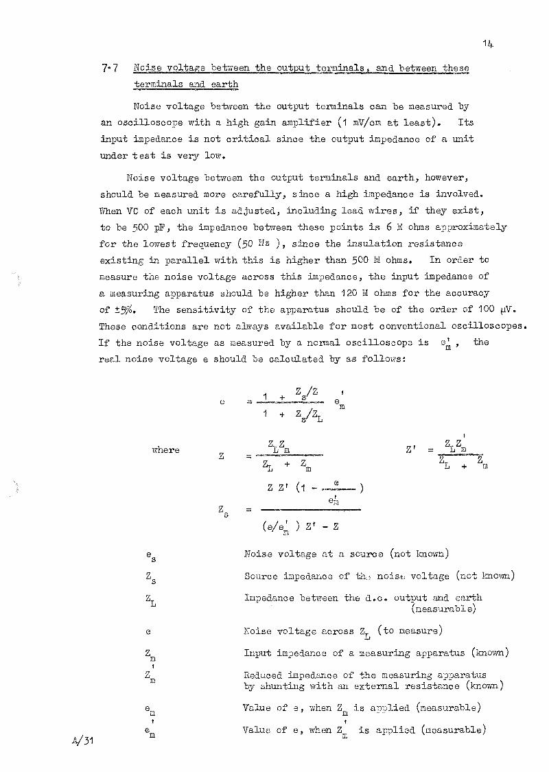
7"7 Noise voltage between the output terminals, and, between these
terminals and earth
Noise voltage between the output terminals can be measured by
an oscilloscope with a high gain amplifier (1 mV/cm at least). Its
input impedance is not critical since the output impedance of a unit
under test is very low.
Noise voltage between the output terminals and earth, however,
should, be measured, more carefully^ since a high impedance is involved.
When YC of each unit is adjusted, including lead wires, if they exist,
to be 500 pF, the impedance between these points is 6 M ohms approximately
for the lowest frequency (50 Hz ), since the insulation resistance
existing in parallel with this is higher than 500 M ohms. In order to
measure the noise voltage across this impedance, the input impedance of
a measuring apparatus should be higher than 120 M ohms for the accuracy
of ±5%» The sensitivity of the apparatus should be of the order of 100 pV.
These conditions are not always available for most conventional oscilloscopes,
If the noise voltage as measured by a normal oscilloscope is , the
real noise voltage e should be calculated by as follows:
1 + s
'L
!
where „ Z' = ^^m
2^ + Zm %!, + %m
Z Z' (1 .
(e/eZ ) Z' m
e Noise voltage at a souroe (not known)
Zg Source impedance of tho noisk voltage (not known)
Z^ Impedance between the d.o. output and earth
(measurable)
e Noise voltage across (to measure)
Z Input impedance of a measuring apparatus (known)
f
Z Reduced impedance of the measuring apparatus by shunting with an external resistance (known)
V31
e Value of e, when Z is applied (measurable)
' I e^ Value of e* when Z^ is applied (measurable)

15
8* Arrangement of coamon parts for all the units
Common parts for all the units are shown in Pig, 17. A
common step-down transformer, TC, is used for every 5O units, The
secondary of this transformer is earthed through near the electrical
centre of VRB for balancing all the undesirable voltages of gO Kz
component appearing at the outputs. The primary of this transformer
can be operated directly from a power line of 24-0 V m s ± 10^, if the
stability of the output voltage is not required to be higher than
±0'1^. However, a stabilization of the primary voltage has many
advantages in addition to an improvement of the output voltage stability
by one order. Therefore, a solid-state a.c, voltage stabilizer which
has ±0*2^ stability including line freguaacy fluotuations has been
used in common for all the step-down transformers. This can cover
up to 8 transformers (U-00 output units) at the maximum, but is
usually used with if transformers (200 output units), the rest of the
power being used, for other apparatus. This arrangement makes the
whole system flexible, and the oost per unit becomes moat economical*
9. Conclusion
The overall characteristics of the whole system are summarized
in Table 5« These satisfy all the conditions described in Chapter 1,
Acknowledgements
This work is part of Project 'Storm Surges in the North Sea'
oarried out at the National Institute of Oceanography, under the
Director, Dr. G,E»R, Deacon, F.E.S,
Construotion of the actual apparatus has been carried out by
Mr. &,H, Balchin,
16
•PS
p
Li
Rectifier & voltage • r stabilizer —o' 1 !
Load ——41 T- /WV-
g:) 2.
—ji- —o—I f
7 ^ Fig, 1(a) A oonventional arrangement, (b) Simplified, a.o. equivalent.
II •Mr ,,.| I . MMW' • — ! II mmmmm mmmo m—1» wmmm ii —" .
/ I "
! T I ,
T_ t
Reotifier l--lt"t--ll-E & voltage !( Btabilizer L_y
Load.
2,/ Y V -777" " -7^ -^-
Pig. 2(a) Double eoreened arrangement, (b) Simplified, a.o. equivalent.
Common i transformer
C iL Unit Outer screen
50 Hz
: Inner screen /VVVWi- Wv
Voltage stabilizer
Fig. 3 An equivalent circuit for noise voltagem.
2 J)
Lead, for . Z
f !e
ofi ] 0 1
screen
0
Leads for " ^ ;;::Ad.nding
( a ) S c r e e n and core
— j " — — J - — ^ — y — ^aaap) |
(b) Equvalent oirouit
I 0 10 20
t (ma)
Pig. 4 Some waveforms in the circuit shoMi in Pig. 3
2—€>-^f^S^^-e-T€)—^
, V ^ (e) Simplified, equivalent E
4
e
J;
Pig. 5 Vcltrngea induced, in the screen of the secondary winding.
1 7
Input *
1 '£.,1 ^ rf.. ' I —^ I m
Boreen cas^ Inner screen tut^
I r
O --£
ivo. i1 1:
To I J
Outrut
30- 40 * Opened.
Fig, 6 Circuit of one unit
fable 1, List of components for one unit
Manufao Cost per unit Uomponent
aPY51 NPN, silicon, 0.8W 2N3702 /VPN \ silicon, O.j,? 2N2925 PNP, silicon, 0.%? C3K B80G400 Bridge, O.4A
MuUard, Texas G.3. Semikron
0AZ244 Zener, 6'8V, 0'27wl Mullard.
1000 25V MEF 109A1 1000 pf 25V MEF 109A1 10 15V Sub-min.
30-140 pF 5OOV SI4OI 30/140
Hunts Hunts R.S. 7/ingrove
33 n 1*5% 700c F23 a::8T 68 0 1'5W 700c F23 5%ST 470 0 O.^-J 70°C m 5 IK n 0 ' 5 f 70°c m 5 sf.sT 1K n 0'5W 70^0 MR5 5^ST 4'7K ^ O.5W' 700c MR5 5^ST 1K 0 O.23M 55°G MP-Dealer, lin
Transformer: core and clamp self-bonding wire self-bonding wire aluminium foil insulation tape
KX, Unisil 29SWG, 1200" 3ISW&, 1200" 0'001"T
V/elwyn Vfelwyn iVelwyn Veltvyn
V / e l w y n Jelwyn Plessey
Copper clad for p,c.b. Copper clad for scTt^n Outer screen case Inner screen tube Clamp for tube Heat-sink adapter
0'625"T 0'623"T 6908P Cent, for SA3 CB45402/007 1004
Belclere LElfC LE7C
Formica Formica Bddystone Silicagel Plessey Jermyn
Input lead wire, Output lead wire, 2 4BA nylon screws, 2 4BA brass screws, 8 4BA nuts, 2 Grommets and 2 clips. Bracket for p.c.b.
18
End.
Ufre%
4j\r. Polythene
];'oil start
Foil
j Tape
Wind, a coil on a former, using 'LewiGKbond.' self "bonding ifire.
Connect N units of coils in series to 240 V power line for t sec. GO that the coils are sealed, by heating.
Bold.ered. point
tape
Remark
Second. Prim
8WG Ifo. 29
Turns
0.43" 0.34" I A I
B^nd. the coil at four parts ifith Ofrez. Goat the coil with polythene and. seal its end. ath Ofifez.
Wrap the coil with an aluminium foil except the end. part.
Put a flexible sleeve on each lead, irfire, and. put a screen tube on them. Fix them to the coil with p.v.o. tape.
Complete the aluminium foil screen. S^ld.er the screen
tube and. the lead. wire to the foil.
Wrap the coil with a p.v.o. tape.
Ofrez :
0.25" X 2" X 0.001"
Polythene :
0.25" X 24" X 0.001"
Aluminium foil i
4.8" X 2" z 0.001"
Sleeving :
2 " X 0.08" IcLia.)
Screen tube r
1.5" X 0.15" ld.ia.)
Screen should, not malce a closed, circuit around, the magnetic flux. Lead, ifire : 7/40 p.v.o, coverd., 4"
P.v.o. tape :
12" X 0.4" 0,005"
Fig, 7. Process of oonstruoting transformer windings.
1 9
Table 2, Design factors of transformer windings
Secondary Primary
Wire ('L ewm exbond') 31 SW& 29 S7/Q.
Max. current rate 0.127 A 0.174 A
Actual nominal current O'lO A rma O'H A rmg
Number of turns 460 460
Turns per layer 22 27
Number of layers (0'3") 21 i 17
Total length of wire 1200" apprcx. 1200" approx.
Resistance (theoretical) 7"3 ohms 5.3 ohms
Voltage drop at nominal current (theoretical)
.
0«91 V rms 1 0.95 V rms
$
T |cg-
.7r
/'f
Primary
4-
T
. 7^ ^
JL Cs.
T inches 1:- /.4
Seoondory
Pig. 8 DimensionB of windingB of T1
f
ro
T
/.g
t = 16SWG
A = .43 for J/rimary .34 for Beoondary
=-4 ^ h ' inches
Pig, 9 DimenBions of winding formers of T1
20
load.
XSBlStlVG load " lYG^
Nominal
j)40 BigniiioEmt difference between 46OT and 500T
0.
18 20
(V rms)
I Resistive load " 1700.
No load
2",, (V rms)
Pig. 10 Characteristics of Transformer Tl,
Table 3. Uharacteristics of Transformer Tl.
Primary
voltage 6^ Id.O V rms current j. 0.11 A rms power p.n l.gd W rms
Inductance 0.2? E Resistance 7
Secondary voltage ib,0 V rms current o.lO A rms rower Z'.: 1.60 W rms
Inductance 0.2^ E Resistance 10 ^
Efficiency ; 619^
21
Copper olad. 11
Cable olips
AC DC OUT
*..lTylon Gorews
I'he printed, circuit board is shown in a mirror-image view ,for comparison with componentB,
finches)
47D,? J7 IK
e+
'CUK
fC 4-
Copper cla^ for inner y screen , / "t= .'625 /
/ <\
.34 .4
bo
<S :
LY
Printed, dirouit board. 1—
Fig. 11 Arrangement of oomponents
22
g 100 Jjoad. = 1671
Kb load.
16 18 (V rme)
LU
Uj
+0.9g6
16 18 (V rms)
uj
lOV og&
-o,a&
12 14 16 18 rms)
20
wj
lOV 0^
g.
50 60 70 8 0 9 0 100 1 1 0 1 2 0 130 ^ (mA)
Complete unit
Lu lOV 0^
17 IV rms)
-0.956 - 1 0 :o 1 0 2 0 30 40 50 60 70
'^Mi(°C)
Pig, 12 Eleotrioal oharaoteristioB of a unit
23
40.196
Average values are taken from several data.
kj
lOV 0^
-0.19G
Nominal
0 10 20 30 40 50 6 0 70
40.1^
uj lOV 0^
-0.1{6
1 4 15 16 17 18 19 20 f (7 rme)
2 4 0 V 50 Ez <
Voltage oontroller r Unit under test
Voltmeter ±6.CiaG
Pig* 13 Line and. load, stabilities of the output volteige, and. a test method.
24
.4
.3
.2
.1
1 A.: Load at 1-2 B : Load at 3-4 with remote error mensing 0 ; Load at 3-4 without remote error sensing
Ik 51c lOk / (Hz)
50k 100k
Lead wires 23/.00?6" twin, soreened; 33"
4 -Unit under test ^-ITV
cao with dif, amp
sine—waTe oscillator IHz - lOOkEz
Fig, 14 Output impedance of & unit, and test method.
40.01^
Lu lOV 0^
-0.019&
40.2^
+0.1?G
. lOV oy, Lu
-0.1{t
On Off
From At 1-2
At 3 - 4 — i With lead wires
Load
CitO with a.o. balanoed differential amplifier
test
lOOEz
Reed relay with electrostatic screen and neutram lized magnetic coupling
Pig. 15 Output Toltagec responses to loa^ changes,
mid. a test method.
+Oel)b
? lOV
m 17V Ogk —10^
Ko load.
LoacL . l^Tn -
I W
UJ
g 17V OJ
Uj
40.19;
lOV Ogk
—0,19&
$ w u . 17V ov
0 .1 ,3 .4 . ^ 0 if (seo)
#%
No load.
Load. " 167
0 *iL , 4 0 2 4 Y(seo)
8 10 12 1/
Mo load. \\ No Ic »ad.
/ %Loa i " I .67a Load. " ^
167 a
0. @ 1 @ 2 •© 4 ^(Geo)
240 V 50 Ez
Voltag* oontrol und.er
Dif. amp
Tyr"
Pig. 16 Output voltage rei^onaes to line voltage ohang* and. a teat method.
26
240 V rras ± lO/o
1.7 k¥ max
Bolid-state a.c. voltage stabilizer
TO
240 V rras ± 0.2 ^ 1,2 kW max
lb V rms ± 0.29 , 150 W max
Same
To primary of each T1
- # —
V rns V arms 250 J; I r.-'l6 240 230 ij:' pii 220 »—/, iji!
ii'i ,0 210 200
0
Hi! b.2 d!
Details of 'fC
Pig. 17 Common parts for all the unite.
'i'able 4" List of main compononus j.or common part
VS
TG
Component Type
Solid-state a.o. voltage stabilizer, input 21+0 V rmsl 1 1 o u t p u t 240 V rms 1 { BTE-5P 0.2^, 1*2 K W waveform distortion 2 o
Transformers, input 21+0 V rms, output 21"5 V rms, 150 W
.SH4521 (modi-fied)
Unit coat Manufacturer Z'lO .
& s d
Claude L^ons 1 87. 17. 0.
G-arajfoerj* 4* 4. 10.
* As many as required, up to the maximum power rate.
27
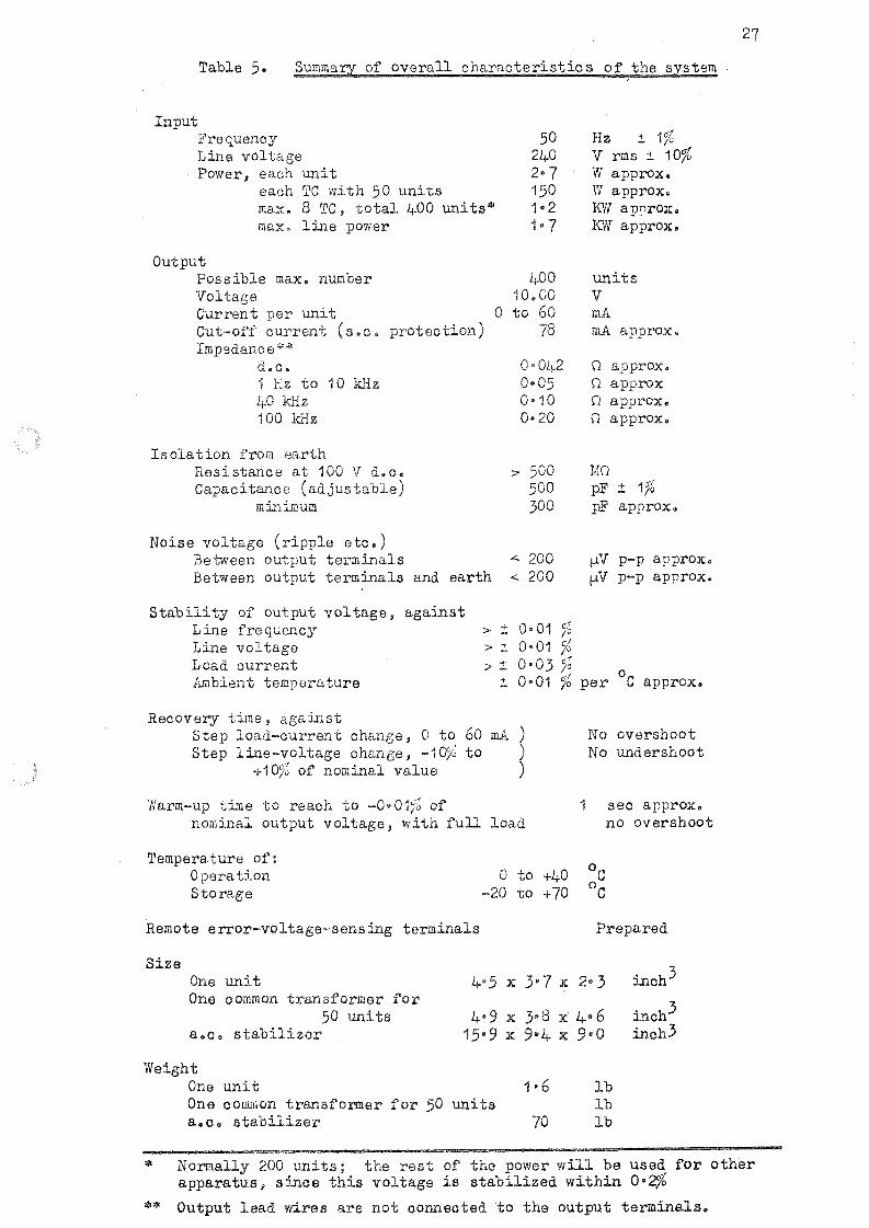
Table 5. Summaiy of overall oharacteristics of the system
Input Frequency 50 Line voltage 2^0 Power, each unit 2*7
each TC with 50 units 150 max. 8 TC, total 400 units* 1*2 max. line power 1'7
Output Possible max. number 400 Voltage 10,00 Current per unit 0 to 60 Cut-off current (s.c, protection) 78 Impedanc e * *
d.c. 0'042 1 Hz to 10 kHz 0«05 40 kHz 0' 10 100 kHz 0.20
Isolation from earth Resistance at 100 V d.o. ? 500 Capaoitanoe (adjustable) 500
minimum 300
Noise voltage (ripple etc.) Between output terminals 200 Between output terminals and earth < 200
Hz 1 1^ V rms 1 10^ W approx. W approx. Mr apnrox. KVf approx.
units V mA mA approx.
n approx. n approx n approx. n approx.
Mn pF 1 1^ pP approx.
pV p-p approx. p-p approx.
Stability of output voltage, against Line frequency Line voltage Load current Ambient temperature
> + 0.01 > 1 0.01 ^ > ± 0.03 ^ 1 0.01 0 per C approx.
Recovery time, against Step load-current change, 0 to 60 mA Step line-voltage change, -10^ to
+10/0 of nominal value
No overshoot No undershoot
Warm-up time to reach to -0.01^ of nominal output voltage, with full load
Temperature of: Operation 0 to +4O Storage -20 to +70
Remote error-voltage-sensing terminals
Size
sec approx. no overshoot
Prepared
One unit 4-5 X 3-7 X 2'3 inoh^ One common transformer for %
50 units 4-9 X 3.8 X 4* 6 iach a,o . stabilizer 15'9 X 9'4 X 9-0 inoh^
Weight One unit 1.6 One common transformer for 5O units a.o« stabilizer 70
lb lb lb
* Normally 200 units; the rest of the power will be used for other apparatus, sinoe this voltage is stabilized within 0 " ^
** Output lead wires are not oonneoted to the output terminals.
28
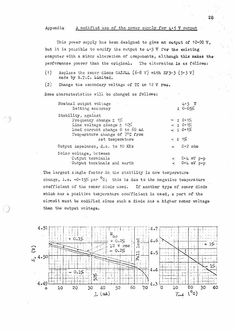
Appendix A modified use of the power supply
This power supply has been designed to give an output of 10*00 V,
but it is possible to modify the output to 4*5 V for the existing
computer with a minor alteration of components, although this makes the
performanoe poorer than the original, The alteration is as follows:
(1) Replaoe the zener diode 0AZ244 (6«8 V) with ZFj*) (3*3 V) made by S.T.C. Limited.
(2) Change the secondary voltage of TC to 12 V rma.
Some characteristics will be changed as follows:
Nominal output voltage Setting accuracy
Stability, against Frequency change 1 1^ Line voltage chazige 1 10^ Load current change 0 to 60 mA Temperature change of 7°C from
set temperature
Output impedanoe, d.c. to 10 KHz
Noise voltage, between Output terminals Output terminals and earth
4'5 V 1 0.05^
± O'l^ 1 O'l^ 1 0'1^
1 1^
0'2 ohm
< 0«4 mV p-p < 0*4 mV p-p
The largest single factor in the stability is now temperature
change, i.e. -O'l^^o per °C; this is due to the negative temperature
coefficient of the zener diode used. If another type of zener diode
which has a positive temperature coefficient is used, a part of the
circuit must be modified since such a diode has a higher zener voltage
than the output voltage.
4.51
m 4.50
4 . 4 9
+ 0.1^ : + 0.2% 12 1/ rms
20 30 40 50 60 70 0 10 20 30 40
7;.^ ( 0) J. (mA)

»-S^ SSmmi.
'r]'%*Xr% 1
Mmrnm^^mWrnS K
l a i ? ® - ? ; ? ® ® ; ' S S I
ligr #
W - j » § Kwk iu'
"vivvS i
' W K } .4; ' B«@0RW4
S/,-,it>i5
:,r;WE i '^J^i 'ii^-j'^'!
A/V^
'Wwpi
t w m %
it;;.,l|.'.. ;,\.\i. i- -J? .<• w m mm
# #5'
' awKi^aam
i
# # # # « ' # « ! # mijMzy/xn \w
%#