Embed Size (px)
Citation preview
A Modeling and Simulation Method of SiC MOSFET Module
Jinyuan Li, Meiting Cui, Shuai Sun and Yujie Du Global energy interconnection research institute co. Ltd.,Changping District, Beijing102209, China
Abstract—In recent years, silicon carbide and other wide band gap semiconductors have become one of the strategic commanding heights in the global high-technology field. As a wide band gap semiconductor, SiC material which can be used to make SiC device is paid much attention in semiconductor and power field due to its advantages. Compared with Si device, SiC device can achieve high switching speed and low on-resistance. Because of the differences in their characteristics, the model of SiC device is different from Si device. In this paper, a modeling and simulation method of a SiC MOSFET module is proposed. Firstly, the physical structure is shown to analyze the source of model parameters; Secondly, according to the relating characteristic curves, the chip model is built; Thirdly, packaging parasitic parameters of SiC MOSFET module are extracted to make the module model more precise; Then, the model of SiC MOSFET module is built and double-pulse simulation circuit is established to observe the switching parameters. Finally, the comparison of simulation and test results is made,which proves the validity of the model and the feasibility of the method.
Keywords—SiC MOSFET; model; simulation; parasitic parameter extraction
I. INTRODUCTION
In recent years, silicon carbide (SiC) and other wide band gap semiconductors have become one of the strategic commanding heights in the global high-technology field. As a wide band gap semiconductor, SiC material has superior electrical characteristics, including wide band gap (2.3eV-3.3eV), high breakdown electric field [(0.8-3.0)x106V/cm], high saturation drift velocity (2x107cm/s) and high heat conductivity (4.9Wcm-1K-1), which can make the SiC device operating in special conditions, such as high temperature, large power and high frequency [1]. The process and application of the SiC device are paid much attention in semiconductor and power field due to its advantages.
Silicon Carbide (SiC) metal-oxide-semiconductor field effect transistor (MOSFET) can achieve high switching speed and low on-resistance at the same time which Si device can’t. Even under high temperature condition, SiC MOSFET can also show excellent electrical properties [2]. The properties above contribute to dramatic reduction of switching loss and the miniaturization of peripheral components. SiC modules integrated with SiC Schottky barrier diode (SBD) realize extremely short reverse recovery time that Si fast recovery diodes (FRD) is hard to achieve, making high switching speed possible. Due to the small amount of reverse recovery charge, the contribution to reducing switching loss and equipment volume is made.
Before engineering application, the electrical system should often be simulated to verify the circuit topology and its control strategy, analyze the dynamic and static characteristics and loss of the SiC MOSFET and evaluate the efficiency and reliability of the whole system. Therefore, it is of great significance for its application to establish a precise SiC MOSFET model. Because of the differences between SiC device and Si device, the model of SiC device is different from the other. A precise device model makes the circuit simulation more meaningful. The significance of modeling and simulation lies in that the parameter measurement of the chips inside the module is difficult or sometimes impossible.
In this paper, a modeling and simulation method of a 1200V/120A SiC MOSFET module is proposed, which is suitable for other types of SiC MOSFET modules. Firstly, the physical structure is shown to analyze the source of model parameters; Secondly, according to the relating characteristic curves, the chip model is built in saber software by applying curve fitting method; Thirdly, packaging parasitic parameters of the SiC MOSFET module are extracted to make the module model more precise; Then, the model of SiC MOSFET module is built and double-pulse simulation circuit is established to observe the switching parameters. Finally, the comparison of simulation and test results is made,which proves the validity of the model and the feasibility of the method.
II. PHYSICAL STRUCTURE OF A SIC MOSFET
A. Physical Structure of a SiC MOSFET
A SiC MOSFET is a type of MOSFET, which applies SiC material in chip design and process for production. Its structure is similar to Si MOSFET, which applies Si material instead of SiC material.
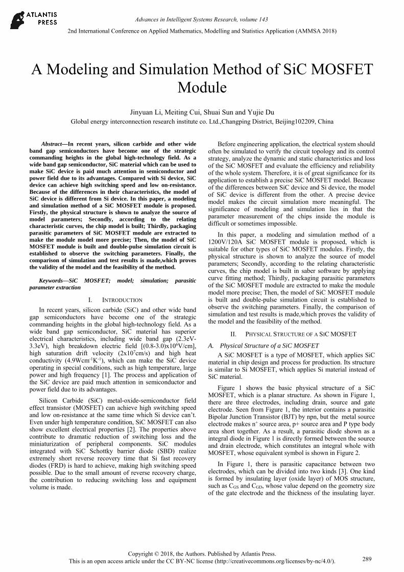
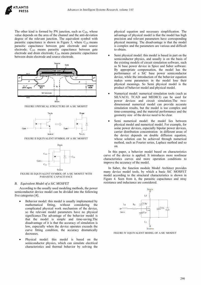
Figure 1 shows the basic physical structure of a SiC MOSFET, which is a planar structure. As shown in Figure 1, there are three electrodes, including drain, source and gate electrode. Seen from Figure 1, the interior contains a parasitic Bipolar Junction Transistor (BJT) by npn, but the metal source electrode makes n+ source area, p+ source area and P type body area short together. As a result, a parasitic diode shown as a integral diode in Figure 1 is directly formed between the source and drain electrode, which constitutes an integral whole with MOSFET, whose equivalent symbol is shown in Figure 2.
In Figure 1, there is parasitic capacitance between two electrodes, which can be divided into two kinds [3]. One kind is formed by insulating layer (oxide layer) of MOS structure, such as CGS and CGD, whose value depend on the geometry size of the gate electrode and the thickness of the insulating layer.
2nd International Conference on Applied Mathematics, Modelling and Statistics Application (AMMSA 2018)
Copyright © 2018, the Authors. Published by Atlantis Press. This is an open access article under the CC BY-NC license (http://creativecommons.org/licenses/by-nc/4.0/).
Advances in Intelligent Systems Research, volume 143
289
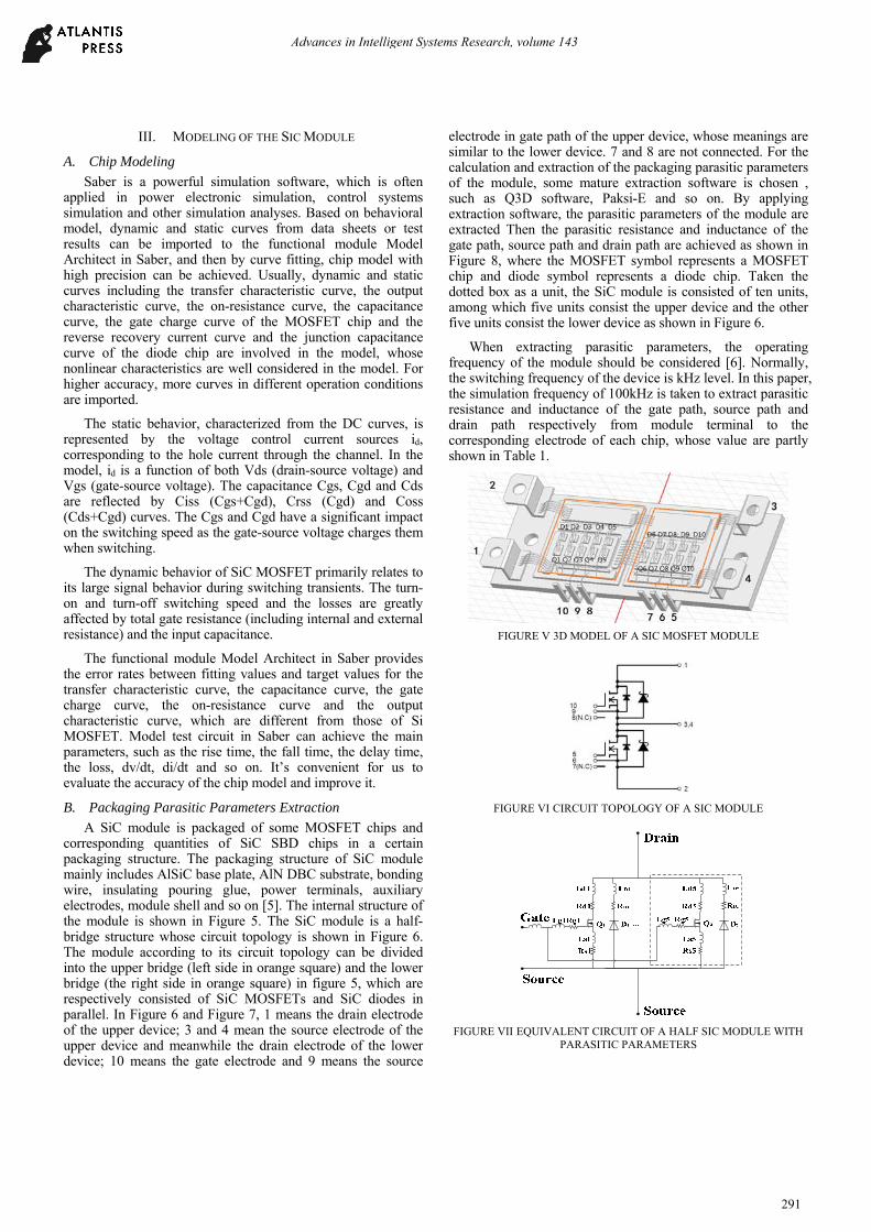
The other kind is formed by PN junction, such as CDS, whose value depends on the area of the channel and the anti-deviation degree of the relevant junction. The equivalent symbol with parasitic capacitance is shown in Figure 3, where CGS means parasitic capacitance between gate electrode and source electrode; CGD means parasitic capacitance between gate electrode and drain electrode; CDS means parasitic capacitance between drain electrode and source electrode.
FIGURE I PHYSICAL STRUCTURE OF A SIC MOSFET
FIGURE II EQUIVALENT SYMBOL OF A SIC MOSFET
Gate
Drain
Source
CGD
CGS
CDS
FIGURE III EQUIVALENT SYMBOL OF A SIC MOSFET WITH
PARASITIC CAPACITANCE
B. Equivalent Model of a SiC MOSFET
According to the usually used modeling methods, the power semiconductor device model can be divided into the following five categories [4].
Behavior model: this model is usually implemented by mathematical fitting, without considering the complicated physical work mechanism of the device, so the relevant model parameters have no physical significance.The advantage of the behavior model is that the model is simple and time-saving.The disadvantage of it is that the accuracy of simulation is low, especially when the device operates exceeds the curve fitting condition, the accuracy dramatically decreases.
Physical model: this model is based on the semiconductor physics, which can simulate electrical characteristics and thermal behavior by solving the
physical equation and necessary simplification. The advantage of physical model is that the model has high precision and relevant parameters have corresponding physical meaning. The disadvantage is that the model is complex and the parameters are various and difficult to obtain.
Semi physical model: this model is based in part on the semiconductor physics, and usually is on the basis of the existing models of circuit simulation software, such as Si base power device in Spice and Saber software. By appropriate compensation, the model has the performance of a SiC base power semiconductor device, while the introduction of the behavior equation makes some parameters in the model lose their physical meanings. So Semi physical model is the product of behavior model and physical model.
Numerical model: numerical simulation tools (such as SILVACO, TCAD and MEDICI) can be used for power devices and circuit simulation.The two-dimensional numerical model can provide accurate simulation results, but the model is too complex and time-consuming, and the material performance and the geometry size of the device need to be clear.
Semi numerical model: the model lies between physical model and numerical model. For example, for some power devices, especially bipolar power devices, carrier distribution concentration in different areas of the device depends on double diffusion equation, whose solution can be achieved through numerical method, such as Fourier series, Laplace method and so on.
In this paper, a behavior model based on characteristics curve of the device is applied. It introduces more nonlinear characteristics curves and more operation conditions to improve the accuracy of the model.
In Saber, the function module Model Architect provides many device model tools, by which a basic SiC MOSFET model according to the structural characteristics is shown in Figure 4. Seen from it, the parasitic capacitance and stray resistance and inductance are considered.
FIGURE IV EQUIVALENT MODEL OF A SIC MOSFET
Advances in Intelligent Systems Research, volume 143
290
III. MODELING OF THE SIC MODULE
A. Chip Modeling
Saber is a powerful simulation software, which is often applied in power electronic simulation, control systems simulation and other simulation analyses. Based on behavioral model, dynamic and static curves from data sheets or test results can be imported to the functional module Model Architect in Saber, and then by curve fitting, chip model with high precision can be achieved. Usually, dynamic and static curves including the transfer characteristic curve, the output characteristic curve, the on-resistance curve, the capacitance curve, the gate charge curve of the MOSFET chip and the reverse recovery current curve and the junction capacitance curve of the diode chip are involved in the model, whose nonlinear characteristics are well considered in the model. For higher accuracy, more curves in different operation conditions are imported.
The static behavior, characterized from the DC curves, is represented by the voltage control current sources id, corresponding to the hole current through the channel. In the model, id is a function of both Vds (drain-source voltage) and Vgs (gate-source voltage). The capacitance Cgs, Cgd and Cds are reflected by Ciss (Cgs+Cgd), Crss (Cgd) and Coss (Cds+Cgd) curves. The Cgs and Cgd have a significant impact on the switching speed as the gate-source voltage charges them when switching.
The dynamic behavior of SiC MOSFET primarily relates to its large signal behavior during switching transients. The turn-on and turn-off switching speed and the losses are greatly affected by total gate resistance (including internal and external resistance) and the input capacitance.
The functional module Model Architect in Saber provides the error rates between fitting values and target values for the transfer characteristic curve, the capacitance curve, the gate charge curve, the on-resistance curve and the output characteristic curve, which are different from those of Si MOSFET. Model test circuit in Saber can achieve the main parameters, such as the rise time, the fall time, the delay time, the loss, dv/dt, di/dt and so on. It’s convenient for us to evaluate the accuracy of the chip model and improve it.
B. Packaging Parasitic Parameters Extraction
A SiC module is packaged of some MOSFET chips and corresponding quantities of SiC SBD chips in a certain packaging structure. The packaging structure of SiC module mainly includes AlSiC base plate, AlN DBC substrate, bonding wire, insulating pouring glue, power terminals, auxiliary electrodes, module shell and so on [5]. The internal structure of the module is shown in Figure 5. The SiC module is a half-bridge structure whose circuit topology is shown in Figure 6. The module according to its circuit topology can be divided into the upper bridge (left side in orange square) and the lower bridge (the right side in orange square) in figure 5, which are respectively consisted of SiC MOSFETs and SiC diodes in parallel. In Figure 6 and Figure 7, 1 means the drain electrode of the upper device; 3 and 4 mean the source electrode of the upper device and meanwhile the drain electrode of the lower device; 10 means the gate electrode and 9 means the source
electrode in gate path of the upper device, whose meanings are similar to the lower device. 7 and 8 are not connected. For the calculation and extraction of the packaging parasitic parameters of the module, some mature extraction software is chosen , such as Q3D software, Paksi-E and so on. By applying extraction software, the parasitic parameters of the module are extracted Then the parasitic resistance and inductance of the gate path, source path and drain path are achieved as shown in Figure 8, where the MOSFET symbol represents a MOSFET chip and diode symbol represents a diode chip. Taken the dotted box as a unit, the SiC module is consisted of ten units, among which five units consist the upper device and the other five units consist the lower device as shown in Figure 6.
When extracting parasitic parameters, the operating frequency of the module should be considered [6]. Normally, the switching frequency of the device is kHz level. In this paper, the simulation frequency of 100kHz is taken to extract parasitic resistance and inductance of the gate path, source path and drain path respectively from module terminal to the corresponding electrode of each chip, whose value are partly shown in Table 1.
FIGURE V 3D MODEL OF A SIC MOSFET MODULE
FIGURE VI CIRCUIT TOPOLOGY OF A SIC MODULE
FIGURE VII EQUIVALENT CIRCUIT OF A HALF SIC MODULE WITH PARASITIC PARAMETERS
Advances in Intelligent Systems Research, volume 143
291
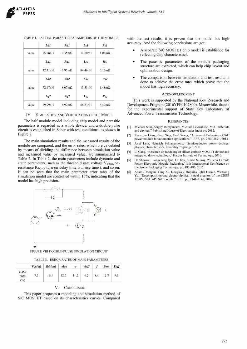
TABLE I. PARTIAL PARASITIC PARAMETERS OF THE MODULE
Ld1 Rd1 Ls1 Rs1
value 75.78nH 9.35mΩ 11.50nH 1.04mΩ
Lg1 Rg1 LD1 RD1
value 32.31nH 6.95mΩ 84.46nH 6.13mΩ
Ld2 Rd2 Ls2 Rs2
value 72.17nH 8.07mΩ 13.53nH 1.48mΩ
Lg2 Rg2 LD2 RD2
value 29.99nH 6.92mΩ 86.23nH 6.42mΩ
IV. SIMULATION AND VERIFICATION OF THE MODEL
The half module model including chip model and parasitic parameters is regarded as a whole device, and a double-pulse circuit is established in Saber with test conditions, as shown in Figure 8.
The main simulation results and the measured results of the module are compared, and the error rates, which are calculated by means of dividing the difference between simulation value and measured value by measured value, are summarized to Table 2. In Table 2, the main parameters include dynamic and static parameters, such as the threshold gate voltage Vgs(th), on-resistance Rds(on), turn-on delay time tdon, rise time tr and so on. It can be seen that the main parameter error rates of the simulation model are controlled within 15%, indicating that the model has high precision.
FIGURE VIII DOUBLE-PULSE SIMULATION CIRCUIT
TABLE II. ERROR RATES OF MAIN PARAMETERS
Vgs(th) Rds(on) tdon tr tdoff tf Eon Eoff
error rate (%)
7.2 6.1 12.6 11.5 6.5 8.4 13.8 9.6
V. CONCLUSION
This paper proposes a modeling and simulation method of SiC MOSFET based on its characteristics curves. Compared
with the test results, it is proven that the model has high accuracy. And the following conclusions are got:
A separate SiC MOSFET chip model is established for reflecting chip characteristics.
The parasitic parameters of the module packaging structure are extracted, which can help chip layout and optimization design.
The comparison between simulation and test results is done to achieve the error rates which prove that the model has high accuracy.
ACKNOWLEDGMENT
This work is supported by the National Key Research and Development Program (2016YFE0102800). Meanwhile, thanks for the experimental support of State Key Laboratory of Advanced Power Transmission Technology.
REFERENCES [1] Michael Shur, Sergey Rumyantsev, Michael Levinshtein, “SiC materials
and devices,” Publishing House of Electronics Industry, 2012.
[2] Zhenxian Liang, Puqi Ning, Fred Wang, “Advanced Packaging of SiC power module for automotive applications,” IEEE, pp. 2884-2891, 2013
[3] Josef Lutz, Heinrich Schlangenotto, “Semiconductor power devices: physics, characteristics, reliability,” Springer, 2011.
[4] Li Gang, “Research on modeling of silicon carbide MOSFET device and integrated drive technology,” Harbin Institute of Technology, 2016.
[5] He Shaowei, Longcheng Que, Lv Jian, Simon S. Ang, “Silicon Carbide Power Electronic Module Packaging,”16th International Conference on Electronic Packaging Technology, pp. 483-486, 2015.
[6] Adam J Morgan, Yang Xu, Douglas C Hopkins, Iqbal Husain, Wensong Yu, “Decomposition and electro-physical model creation of the CREE 1200V, 50A 3-Ph SiC module,” IEEE, pp. 2141-2146, 2016.
Advances in Intelligent Systems Research, volume 143
292