Embed Size (px)
Citation preview

A Microelectronic Design for Low-Cost Disposable
Chemical Sensors
by
Stuart S. Laval
Submitted to the Department of Electrical Engineering and ComputerScience
in partial fulfillment of the requirements for the degree of
Master of Engineering in Electrical Engineering and Computer Science
at the
MASSACHUSETTS INSTITUTE OF TECHNOLOGY
May 2004
2004. All rights reserved. The author herebygrants MIT permission to reproduce and distribute public paper and
electronic copies of thesis document in whole or in part. M INS- E
OF TECHNOLOGY
JUL 2 1)2004
Author ........ ............. LIBRARIES
Department of Electrical Engineering and Computer Science
May 14, 2004
C ertified by ..............................Eric Hildebrant
Principal Member of Technical Staff, Draper LaboratoryThesis Supervisor
Certified by .........................James K. Roberge
Professor of2Electrical Engineering, MITThfesi-rAdfvfsor
Accepted by ..............Arthur C. Smith
Chairman, Department Committee on Graduate Students
BARKER

ri
2

A Microelectronic Design for Low-Cost Disposable Chemical
Sensors
by
Stuart S. Laval
Submitted to the Department of Electrical Engineering and Computer Scienceon May 14, 2004, in partial fulfillment of the
requirements for the degree ofMaster of Engineering in Electrical Engineering and Computer Science
Abstract
This thesis demonstrates the novel concept and design of integrated microelectronicsfor a low-cost disposable chemical sensor. The critical aspects of this chemical sensorare the performance of the microelectronic chip and how this chip integrates andinterfaces with the resistive sensors that detect chemicals. The design, simulation, andimplementation of a low-power CMOS microelectronic analog measurement systemand integration with the resistive chemical sensors is described. The overall goal isto produce a microelectronic design that can be fabricated, tested, and manufacturedby an outside semiconductor vendor.
Thesis Supervisor: Eric HildebrantTitle: Principal Member of Technical Staff, Draper Laboratory
Thesis Advisor: James K. RobergeTitle: Professor of Electrical Engineering, MIT
3

4

ACKNOWLEDGMENTS
This thesis was prepared at The Charles Stark Draper Laboratory, Inc., under T-IRD-04-0-5042.
Publication of this thesis does not constitute approval by Draper or the sponsoring agencyof the findings or conclusions contained herein. It is published for the exchange andstimulation of ideas.
-----------------~w~- ------------- --------- ----------
(Author's signature)
I have been very fortunate and am extremely thankful for all the help and opportunities Ihave received throughout my journey at MIT. First, I would like to thank DraperLaboratory for the opportunity to research for my graduate education and complete a thesis.Secondly, I would like to commend the John Williams for proposing the concept behindthis thesis and Ryan Prince for her amazing support and mentorship with the overalldevelopment design for my chip. I am very gracious for having the opportunity to workwith them and contribute to their group.
I would also like to thank the various people who helped substantially with my growth as acircuit design engineer. First, Eric Hildebrandt for being a tremendous teacher andpromoter of analog circuit design. I would not have been caught up to speed on the analogintegrated circuit fundamentals without him. Secondly, I would like to thank Professor JimRoberge for his insightful guidance on this thesis and on possible career options. Thirdly, Iwould like to thank Ji-Jon Sit and Professor Rahul Sarpeshkar for providing the TannerEDA software and lots of feedback and design strategies for my chip design. I do not knowwhere I would be now without Ji-Jon's incredible CAD tool support for the simulations,layout, and verification of my chip design.
Finally, I would like to thank my friends and family for always being there for me,especially when times were rough. I most dearly appreciate the support and love from myparents as they have been the biggest role models in my life. I credit my passion forlearning and drive for success to my father. I deeply thank my mother for helping meappreciate the simple things in life. Lastly, I thank my brother for his comical humor andhis competitive nature that has always kept me on my toes.


Contents
1 Introduction 13
1.1 Background . . . . . . . . . . . . . . . . . . . . . . . . . . . . . . . . 14
1.2 Types of Sensors . . . . . . . . . . . . . . . . . . . . . . . . . . . . . 16
1.2.1 pH Based Chemical Sensor . . . . . . . . . . . . . . . . . . . . 16
1.2.2 Electronic Based Sensor . . . . . . . . . . . . . . . . . . . . . 16
1.2.3 Design Flow . . . . . . . . . . . . . . . . . . . . . . . . . . . . 17
2 Sensor Design 21
2.1 Sensor Overview . . . . . . . . . . . . . . . . . . . . . . . . . . . . . 21
2.1.1 Power Supply . . . . . . . . . . . . . . . . . . . . . . . . . . . 22
2.1.2 Sensor . . . . . . . . . . . . . . . . . . . . . . . . . . . . . . . 22
2.1.3 Display . . . . . . . . . . . . . . . . . . . . . . . . . . . . . . 22
2.2 Electronic Prototype . . . . . . . . . . . . . . . . . . . . . . . . . . . 23
2.3 Microelectronics . . . . . . . . . . . . . . . . . . . . . . . . . . . . . . 24
3 Microelectronic Measurement System 27
3.1 W heatstone Bridge . . . . . . . . . . . . . . . . . . . . . . . . . . . . 27
3.2 Voltage Reference . . . . . . . . . . . . . . . . . . . . . . . . . . . . . 28
3.3 Auto-zero Technique . . . . . . . . . . . . . . . . . . . . . . . . . . . 30
3.4 Digital Components . . . . . . . . . . . . . . . . . . . . . . . . . . . . 30
4 Operational Amplifier 35
4.1 Design of Operational Amplifier . . . . . . . . . . . . . . . . . . . . . 35
7

4.1.1 Derivation of Compensation . . . . . . . . . . . . . . . . . . . 35
4.1.2 Transistor Sizing of Operational Amplifier . . . . . . . . . . . 38
4.2 Operational Amplifier Simulation Results . . . . . . . . . . . . . . . . 39
5 Chip Verification and Layout 43
5.1 Total Chip Simulation . . . . . . . . . . . . . . . . . . . . . . . . . . 43
5.1.1 The Positive Terminal . . . . . . . . . . . . . . . . . . . . . . 45
5.1.2 The Negative Terminal . . . . . . . . . . . . . . . . . . . . . . 45
5.1.3 The Analog Component . . . . . . . . . . . . . . . . . . . . . 45
5.1.4 The Output Logic. . . . . . . . . . . . . . . . . . . . . . . . . 46
5.2 Total Chip Simulation Results . . . . . . . . . . . . . . . . . . . . . . 48
5.3 Chip Integration . . . . . . . . . . . . . . . . . . . . . . . . . . . . . 49
5.4 CMOS Layout . . . . . . . . . . . . . . . . . . . . . . . . . . . . . . . 51
6 Conclusion 53
6.1 Summary . . . . . . . . . . . . . . . . . . . . . . . . . . . . . . . . . 53
6.2 Future Work . . . . . . . . . . . . . . . . . . . . . . . . . . . . . . . . 53
A SPICE netlist file 55
8

List of Figures
1-1 Biogenic amines from amino acids. . . . . . . . . . . . . . . . . . . . 15
1-2 Color indictors with pH scale. . . . . . . . . . . . . . . . . . . . . . . 17
1-3 Prototype: milk cap sensor. . . . . . . . . . . . . . . . . . . . . . . . 18
1-4 Prototype: digital sensor device. . . . . . . . . . . . . . . . . . . . . . 18
1-5 Top-level view of the sensor. . . . . . . . . . . . . . . . . . . . . . . . 19
2-1 Top-level view of the sensor revisited. . . . . . . . . . . . . . . . . . . 21
2-2 Packaging concept: milkcap. . . . . . . . . . . . . . . . . . . . . . . . 23
2-3 A resistive Wheatstone full-bridge network . . . . . . . . . . . . . . . 25
2-4 An ideal op-amp with buffers and LEDs at the output. . . . . . . . . 25
3-1 Wheatstone bridge network with reference. . . . . . . . . . . . . . . . 29
3-2 Autozeroing system. . . . . . . . . . . . . . . . . . . . . . . . . . . . 31
3-3 Expected system output after auto-zeroing circuit for AR= 200Q. . . 31
3-4 Series of 11 switches connected to 100KQ and 100Q resistors. . . . . . 32
3-5 Schematic of shifting registers. . . . . . . . . . . . . . . . . . . . . . . 32
3-6 Schematic of storing registers. . . . . . . . . . . . . . . . . . . . . . . 33
3-7 Schematic of a switch. . . . . . . . . . . . . . . . . . . . . . . . . . . 33
4-1 Op-Amp schematic. . . . . . . . . . . . . . . . . . . . . . . . . . . . . 36
4-2 Op-Amp schematic with transistor sizes. . . . . . . . . . . . . . . . . 39
4-3 Frequency response of op-amp: magnitude plot. . . . . . . . . . . . . 41
4-4 Frequence response op-amp: phase plot. . . . . . . . . . . . . . . . . 41
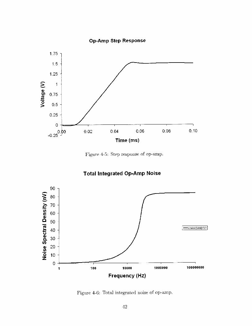
4-5 Step response of op-amp. . . . . . . . . . . . . . . . . . . . . . . . . . 42
9

4-6 Total integrated noise of op-amp. . . . . . . . . . . .4
Total system block diagram. . . . . . . . . . . . . .
System output for AR= 200Q. . . . . . . . . . . . .
System Output after logic for AR= 200Q. . . . . .
Chip Output for AR= 500Q .. . . . . . . . . . . . .
Total Chip with bondpads and off-chip components.
Layout of op-amp in common centroid. . . . . . . .
Total chip layout of CMOS measurement system. .
10
5-1
5-2
5-3
5-4
5-5
5-6
5-7
. . . . . . . 44
. . . . . . . 47
. . . . . . . 47
. . . . . . . 48
. . . . . . . 50
. . . . . . . 52
. . . . . . . 52
42

List of Tables
4.1 Table of transistor characteristics . . . . . . . . . . . . . . . . . . . . 40
4.2 Summary of gain for both stages of the op-amp . . . . . . . . . . . . 40
4.3 Summary of simulation results of the op-amp. . . . . . . . . . . . . . 40
5.1 Table of Results . . . . . . . . . . . . . . . . . . . . . . . . . . . . . . 49
5.2 Table of off-chip clock rise times . . . . . . . . . . . . . . . . . . . . . 50
11

12

Chapter 1
Introduction
There is a strong demand for chemical sensors, which are widely used for hazardous
chemicals, oil exploration, air quality, and process control applications. This thesis
presents a sensor comprised of a chemical coating, electrical transduction mechanism,
power source, logic chip and 10-level readout. A bar type readout (similar to an
analog battery tester) may also be employed. A cost analysis has been performed on
the components and it has been determined that these sensors can be mass produced
for $.10-$.25, making this approach economically feasible. A second embodiment of
this device utilizes a colorimetric readout. Some specific applications are to sense sour
milk, e-coli in beef, salmonella in chicken, botulism in canned goods, and drinking
water contamination. The estimated cost for a system employing only a chemically-
driven colorimetric readout is $.01 since the CMOS chip and battery is not required.
The objective of this research is to design a low-power microelectronic chip in
CMOS technology to interface and to integrate with these resistive chemical sensors.
However, before the design and implementation of the CMOS microelectronics begins,
an electronic prototype of the device, interfaced with the resistive sensors, must be
first characterized in order to determine the specifications of this system. With the
specifications from characterization of the sensor, the CMOS mixed-signal (analog
and digital) chip can be designed and simulated. Furthermore, a power, timing (step
response and clocking), and noise analysis will be required to gauge the theoretical
functionality of the chip. The final objective of this work is to produce a CMOS
13

mixed signal chip that can be fabricated, tested, and integrated with the chemical
sensor.
Chapter one provides a brief background of the purpose and use of the chemical
sensor.
Chapter two describes the sensor design as well as the prototype involved in the
characterization of the resistive sensor.
Chapter three describes the design of the microelectronic measurement system
and how it was implemented.
Chapter four illustrates the design, implementation, and the performance of the
operational amplifier, which is the most important building block of the CMOS mi-
croelectronic system.
Chapter five displays the performance and results of the simulation of the total
chip as well as the the interface and integration of the chip with the packaging of the
entire sensor.
1.1 Background
The World Health Organization reports that 3.2 million children under five years
of age die of food poisoning-related illnesses each year. In the United States alone,
millions of cases of food poisoning occur annually; tens of thousands requiring hos-
pitalization. More than one thousand of these cases are fatal in the populations,
mostly elderly and children [5]. The most fundamental and efficient way to attack
this prodigious public health concern is to produce a simple vapor sensor that can
determine the degree of bacterial decomposition in meats, fish, and poultry. In order
to understand how the chemical sensor detects the degree of bacterial content and
contamination, it is important to examine the chemical and biological properties of
proteins, which bacterial contamination feed upon.
Proteins are made from amino acids; when proteins are bacterially decomposed,
they are converted to amines related to these amino acids. The biogenic amines,
cadaverine, putrescine, and histamine, are produced as a result of the breakdown of
14

amino acids by bacteria in rotten meat or fish. According to Rawles et al [1], the
most significant biogenic amine is histamine, which is produced by the breakdown of
the amino acid histidine. Other significant biogenic amines are putrescine which is
produced by the breakdown of glutamine, and cadaverine produced by the breakdown
of lysine.
HO NH
0 H
N
NH2
HistamineHistidine
It4
N
OH
HNZN 0
Arginine
Lysin.
Putrescine
Cadaverine
Figure 1-1: Biogenic amines from amino acids.
As depicted in figure 1-1, the amino acid arginine is converted to biogenic amine
putrescine, lysine to cadaverine and histidine to histamine. The shaded box shows
the group which is converted to a hydrogen.
Fundamentally, putrescine, cadaverine and histamine are responsible for the smell
of rotting protein such as meat and fish. The levels of these amines are related to
the degree of bacterial decomposition. For example, the levels of biogenic amines
15

in fish and crustacea can be used to indicate the degree of decomposition, so that
the higher the concentration, the greater the amount of bacteria decomposition has
occurred [1]. According to FDA guidelines, fish with greater than 50 ppm histamine
are considered spoiled, although poisoning generally occurs when histamine is present
in concentrations greater than 200 ppm. A comparison of the sensory evaluations and
chemical data suggest that putrescine or cadaverine at the 3 ppm level is indicative of
decomposition in aquacultured Penaeid shrimp over a wide range of storage conditions
[1]. It is the goal of this project to produce low-cost vapor sensors for these volatile
biogenic amines which are present at levels up to hundreds of ppm.
1.2 Types of Sensors
Two types of chemical sensors are being considered: a chemically activated, water-
based pH type with built-in color detection and an affinity type with the proposed
CMOS chip, which is similar to Ryan Prince's "disposable, self-administered elec-
trolyte" circuit for Gatorade [2]. This thesis will focus on the latter.
1.2.1 pH Based Chemical Sensor
The pH based amine sensor for vapors is to be applied on Saran wrap (or Styrofoam)
for meat packages to give consumers an indication of meat freshness; this would be
marketed directly to the container manufacturers. Figure 1-2 illustrates the several
possible color indictors for differently chemically coated pH sensors applied to Saram
Wrap or Styrofoam during manufacturing.
1.2.2 Electronic Based Sensor
A CMOS based sensor using an affinity based coating that would change resistance
when exposed to amines is the main focus of this work. As depicted in figure 1-3,
this could be manufactured as a throwaway milk cap (marketed to the milk carton
manufacturer) or as a reusable milk cap (marketed to "Kitchens-R-Us," "Bed Bath
16

1413
12
11 U
10-
>N 0_ (
5E EE4 -
3
2
<D ~C
10-
Figure 1-2: Color indictors with pH scale.
and Beyond," etc.). Alternatively, as shown in figure 1-4, it could be used as a hand-
held meter priced similarly to a digital thermometer and marketed to drug store
chains
1.2.3 Design Flow
The sensor package is comprised of a chemically resistive sensor, which contains a
chemical coating and electrical transduction mechanism, a power source, a CMOS
mixed-signal chip, and 10-level readout display, which indicates the level of resistive
change. A bar type readout (similar to an analog battery tester, i.e. in Duracell) may
also be employed. The design process and top level view of this device is depicted in
figure 1-5.
The essential purpose of this thesis is to design a low-power microelectronic mea-
surement system in CMOS technology, to interface with these resistive biological
17

Figure 1-3: Prototype: milk cap sensor.
Figure 1-4: Prototype: digital sensor device.
18

POWER SOURCE
SENSOR ELECTRONICS DISPLAY
Figure 1-5: Top-level view of the sensor.
sensors. To better understand the design and implementation of the CMOS micro-
electronics, a breadboarded prototype using passive components of the device with
the resistive sensors must be first analyzed in order to calibrate the resolution of the
resistance changes. After a characterization of the sensor determines the specifica-
tions, the analog integrated CMOS chip can be designed and tested'..
The CMOS design process first involves choosing a circuit topology best suited
for the precise measurement of the small resistance changes of the sensor. Once
chosen, hand calculations of the circuit were done to estimate feasible transistor
sizing and solid performance. Next, SPICE simultations were performed until the
circuit's timing, power, and noise specifications were optimized. Once a thorough
power,timing, and noise analysis gauges the theoretical functionality of the chip, the
CMOS system was laid-out using the CAD tool, Tanner tools, in the AMI .50 Am
design process. Tanner Tools will extract theoretical parasitic effects of the CMOS
design to a SPICE netlist, and also extract the CMOS chip layout into GDSII format,
which are the digital instructions for the fabricating process.
Finally, the fundamental objective of this thesis is to design an analog CMOS chip
'Testing will be done by third party semiconductor manufacturer.
19

that could be submitted to the foundry via MOSIS for fabrication in conjunction with
Professor Rahul Sarpashkar's Low-Power Analog VLSI course at MIT. Ultimately, the
chip will be functional, and eventually integrated with the sensors produced at Draper
Laboratory.
20

Chapter 2
Sensor Design
2.1 Sensor Overview
The top-level diagram of the sensor breaks up the affinity-type sensor design into
four aspects: the power source, the resistive sensor, the electronics, and the display.
Even though the main purpose of this project is to design and implement the CMOS
microelectronics for the sensor, it is very important to also briefly go over how the
other three components function or relate with the CMOS chip.
POWER SOURCE
SENSOR ELECTR(OIS
-I
DISPLAY
Figure 2-1: Top-level view of the sensor revisited.
21

2.1.1 Power Supply
Since the sensor has limiting cost factors, the use of a very low-power energy source,
such as a paper battery, is preferable for a low-cost product. This impacts the entire
design and adds further complexity to the analog circuitry in order to sustain band-
width and noise issues. This also complicates the resolution of the resistive sensors
as well as the dynamics of the display. For one application of the sensor, the digital
hand-held device, off-the-shelf batteries can be used.
2.1.2 Sensor
The chemical sensors will be a type of chemically reactive plastic and electrode. It
will have resistive properties that change in the presence of bacteria, amines, sulfur,
and other unwanted conditions. Other variations of the sensors will use changes
in potentiometric or amperometric properties as the instrument of measuring the
presence of unwanted conditions. The CMOS chip will measure this small resistive
change due to the chemical reaction of the amines exposed to the polymer on the
sensor.
2.1.3 Display
The physical appearance of the display will be a continuous meter-like response with
several intermediate states. For example, with a vapor sensor on a milk cap, the
intermediates states will tell the consumer the quality or time left of usage before
spoilage. On the digital hand-held food quality sensor device, the display would
simply report the quantititive quality level. At Draper Laboratory, Megan Owens
illustrated a milk cap sensor, in figure 2-2, as a packaging concept that would embed
such a sensor into everyday food items.
22

TranslucentPlastic Cap
TranslucentElectrochromic EncapsulantInk Indicators
PrintedBattery
Sensor Chip
SensorActive Area
Figure 2-2: Packaging concept: milkcap.
2.2 Electronic Prototype
In order to fully define the issues that arise during the initial evaluation of data
from the resistive sensor, an electronic prototype was developed and tested. This
prototype consisted of a breadboard, resistors, capacitors, voltage regulators, and a
micro-programmable chip with a built-in Analog-to-Digital converter. The purpose
of the microcontroller prototype is to confirm the wheatstone bridge topology. The
chemically resistive sensor was characterized at Draper Laboratory and revealed the
following sensor characteristics:
Nominal Resistance Value = 100KQ
Maximum Resistance Change = 1KQ
Target Resistance Resolution = 1000ppm
As depicted in figure 2-3 , there will be three constant resistors of 100KQ and one
varying resistive sensor, which create a voltage drop between reference voltage nodes
V+ and V-. These reference voltages will be the inputs to an operational amplifier, as
displayed in figure 2-4, which is the most important unit of the CMOS measurement
23

system.
There will be ten light-emitting diodes (LED's), used to describe chemical environ-
ment; each level will correspond to a higher amount of contaminent. Once the range
of resistance values that correspond to a particular resistive resolution is calibrated,
the microelectronic design can commence.
2.3 Microelectronics
Designing a functional chip in CMOS for this sensor is the purpose and goal of this
thesis. The design requires a system-level plan and design before each individual
circuit module can be simulated in SPICE and laid-out using Tanner Tools in the
AMI .50pm process. Because of the simple operation of the chip to detect resistance
values, compare them, and output a certain value that is transmitted to the LED's,
the CMOS microelectronic building blocks could easily just consist of an operational
amplifier (op-amp) with digital standard library cells provided by the AMI. Figure
2-4 shows this operation.
The second part of the CMOS chip design process involves laying out the custom
analog circuit elements. Before any layout can be attempted, successful simulations
in SPICE will determine the theoretical optimal specifications, such as transistor
sizing of MOSFET gate widths and lengths, for each circuit of each block in the
chip. The purpose of layout in CAD Tools is to simplify and facilitate the verification
and fabrication process. In general, an industry-standard CAD tools such as Tanner
Tools insure and enable the user to verify that the schematic-to-layout behavioral
functionality (LVS/DRC) is equivalent before enabling the user's access to extracting
the SPICE netlist and GDSII format. The SPICE netlist is important because it
contains a precise theoretical measurement of the second order parasitic effects in
deep submicron circuit designs. The GDSII format is the set of instructions sent to
the foundry that will fabricate this chip.
24

R=100k
R=100k
R:
R=1
LOOk
V+0K+r
Figure 2-3: A resistive Wheatstone full-bridge network.
V-Ho---- +PAm 0
U)
~x2v-I
Figure 2-4: An ideal op-amp with buffers and LEDs at the output.
25
=
10

26

Chapter 3
Microelectronic Measurement
System
The purpose of this thesis is to design a low-power microelectronic measurement
system for the food quality sensor. When exposed to a particular amine, the active
chemical sensor will swell up, thereby changing resistance. As noted in the previous
section, the nominal resistance of the sensor is 100KQ and has a maximum resistance
change of 1KQ. In addition, the target resolution that the system is required to
distinguish is 1000 ppm or 100Q increments. Therefore, the goal is to design a low-
power CMOS operational amplifier for measuring the small amount of resistive change
of the chemical sensor when exposed to a particular amine from food.
3.1 Wheatstone Bridge
This measurement system is similar to a classical temperature sensing system, which
utilizes a Wheatstone bridge (developed by S.H. Christine in 1833) to model the
system in a balanced configuration while taking a differential measurement across each
side of the bridge [7] . It is commonly used with precision operational amplifiers and
offers an attractive alternative for measuring small resistance changes. The advantage
of this arrangement is that because it allows a sensitive null-detecting system topology,
it is immune to power supply variations and helps significantly improve common mode
27

rejection.
As illustrated in figure 2-3, the basic Wheatstone bridge consists of four resis-
tors connected to form a quadrilateral, a source of excitation (voltage or current)
connected across one of the diagonals, and a voltage detector connected across the
other diagonal. The detector measures the difference between the outputs of the two
voltage dividers connected across the excitation [7]. Essentially, it is measuring the
resistance indirectly by a comparison with a similar resistance. For the purposes of
this measurement system, the sensor will be modeled in a "single-element varying
bridge" with all four resistors having a nominal value of 100KQ [7]. With the current
resolution of 1000 ppm or 0.1 percent of the nominal resistance, the voltage change
measured across V+ and V- terminals is simply derived by:
100KQ + AR 100 KQ100KQ + 100KQ + AR 100KQ + lOOKQ
= -g ( R _ -as)VDD (-1
100KQ
1 AR
4 100KQ )VDD
Since we are using a power supply, VDD, of 3V, then:
V+ - V- = 0.75mV (3.2)
With this small voltage resolution, we will need an op-amp with at least the following
high DC gain:
3V_A 0 > V 4000 (3.3)-0.75mV
3.2 Voltage Reference
A variable digital-to-analog conversion scheme, using switches and shift registers,
as illustrated in figure 3-1, was used to control voltage reference level. Since the
maximum change in resistance is approximately 1KQ, the differential voltage can
be measured and compared in ten increments of 100Q that correspond to 0.75mV
28

R=100k R=100k
\f- V+0
R=100k R=100K+r I
f- C 0
rk -H
-H
4H
COCO
Figure 3-1: Wheatstone bridge network with reference.
level changes. Therefore, since the Wheatstone bridge is immune to power supply
variations and is useful in null-detecting arrangements, the digital-to-analog converter
switching method can be incorporated on the right side of the bridge by adding eleven
switches for the ten corresponding levels of 100Q increments. These switches (figure 3-
4) and shift registers (figure 3-5) are explained later in section 3.4. Under the current
scheme, ideally an op-amp with a high enough gain could simply compare each level
as each switch, which indicates the reference level, is adjusted to a higher resistance
level. However, realistically, there is a significant input offset error to most op-amps
of around 5-10 mV. Unfortunately, this could require an exhaustive calibration of the
switches and is not practical for this design.
29

3.3 Auto-zero Technique
To eliminate the input offset error problem of the CMOS operation amplifier due
to external and micro-fabrication factors, an auto-zeroing method is proposed as
depicted in figure 3-2. This system, which initially sets switch 1 on the V_ terminal,
requires a closed-loop unity-gain stable, high-gain, operational amplifier that uses
negative feedback to store the offset error and V_ on a 10pF capacitor during the
on-phase of a 50% duty cycle of switch 2. During the off-phase of both switches,
switch 1 is set to V+, while the analog component becomes an open-loop operational
amplifier (also known as a comparator) that compares V+ to the charge stored on
the capacitor as a reference that includes the offset. As a result, the offset error of
the amplifier is nullified. Figure 3-3 shows expected system output after auto-zeroing
circuit for AR= 200Q.
3.4 Digital Components
The digital components of this system in many ways are as critical as the analog
component. The digital system is composed of shifting registers and storing registers.
The shift registers, shown in figure 3-5, essentially include one preset D-Flip-Flop
(DFF) and ten preclear DFFs in a sequential series, where the output of each flip-
flop, Q, controls the voltage reference level of the switches on the bridge. As displayed
in figure 3-4, each sequence of outputs from the 11 DFFs can be thought of as the
11-bit input vector of the 11 switches'. Initially, the first DFF is set to 1, while the
remaining ten DFFs are set to 0, yielding an input sequence of 10000000000 for the
11 switches. Therefore, the first switch that is only connected to the 100KQ resistor
is on, while the other switches are off. For every clock cycle, because of the sequential
arrangement, the 1 is passed to the next DFF, while the other DFF's are 0. However,
the eleventh DFF passes a 0 to the first DFF to change its output to 0, yielding a
01000000000 input vector for the 11 switches. This leaves only one DFF on and,
therefore, the next 100 level is added to the reference level during each clock cycle.
'Each switch, displayed in figure 3-7, has a W/L = 100/2, which yields an on-resistance of 20Q.
30

Switch 1
V-0
,
+
Op-Amp -
Switch 2
OpF
Figure 3-2: Autozeroing system.
System output for AR = 200 Ohms
"O" "OfF"I1 "n,. 0.1 0.2Phase Phas
ID 1f
-Vout
-Clk
0.3 0.4 0.5 0.6 0.7 0.8
Time (ms)
Figure 3-3: Expected system output after auto-zeroing circuit for AR= 200Q.
31
0
U)cmF-1
3
2.5
2
4)15-
0.5 -
0*
-0.5 -
I
------------- --------------

On the other hand, the storing registers are positive edged triggered D-flip-flops
which correspond to each switch depending on the clock period. This design, as illus-
trated in figure 3-6, is quite simple as the input clock signals to each DFF corresponds
to a particular clock period on a particular level of the switch on the reference.
R=1 OOK R=1 00V_
'C::XIC-)4-J
_H _H
R=100
zc9 A&0
Figure 3-4: Series of 11 switches connected to 100KQ and 100Q resistors.
resetCLB CLB
- DATA. Q - -DATA Q - -DATA Q 4
-> QB - -> QB -O -> QBolk PRB ,es
reset
resetCLB
x 7 DATA Q> QB
clk
Figure 3-5: Schematic of shifting registers.
32

reset
CLM outlODATA Q
inclklO
x7reset
CLB out2DATA Q
inclk2 s
reset
CLE outiDATA Q
cl-l> QB -
Figure 3-6: Schematic of storing registers.
qb
Figure 3-7: Schematic of a switch.
33

34
Chapter 4
Operational Amplifier
For this design, it is clear to choose an operational amplifier (op-amp) configuration
that has a high open-loop gain, yet is closed-loop unity-gain stable with a settling time
less than 100ms. A robust and simple design is also preferred in ordered to ensure
a high-gain first stage for low noise behavior. For simplicity, a two-stage op-amp
(figure 4-1) is chosen to help with the low-power energy requirement. It also makes
compensation easier to achieve a 60 degree phase margin at the gain bandwidth.
4.1 Design of Operational Amplifier
It is important to briefly discuss the key design decisions and constraints in order to
meet feasible specifications for a high-gain unity-gain stable op-amp. The approach
utilized in this design process is very similar to the one used in Allen and Holberg's
CMOS Analog Design [4]. Since a robust two-stage op-amp configuration has already
been chosen, the amount of compensation and the sizing of the transistors are the
main issues in the design.
4.1.1 Derivation of Compensation
Before deriving the type and amount of compensation, it is necessary to know the
locations of the poles and zeros in the op-amp. A key design choice, that makes this
35

M3 D--r-CM4 -CM6
Ib asM1 M2 -cc ~- CL
M7 M8 M5
Figure 4-1: Op-Amp schematic.
circuit capable of compensation by only using a simple miller capacitor, is to size the
following transistors in equal pairs:
M1 = M2 (4.1)
M3 = M4 (4.2)
M7 = M8 (4.3)
With the matching differential inputs and the common source amplifier pair, the
system will have the following poles and zero [4, p. 270]:
Pi - (9ds2 + gds4)(9ds6 + gds7) (44)Ym6 0
c
P2 = 9m6 (4.5)CL
36

and
z1 = 9m6 (4.6)Cc
where pi is the miller pole after the first stage, P2 is the output pole after the second
stage, and zi is the compensating zero made with Cc. The unity-gain bandwidth,
GB, which is the frequency when the magnitude of the open loop gain equals 0, is
found to be [4]:
GB m2 (47)Cc
In order to obtain the amount of capacitance needed for a unity-gain stable op-
amp, bandwidth relationships must be first established. First of all, the absolute
value of P2 needs be greater than GB, which implies:
rm2 < 9m6 (4.8)cc CL
Secondly, to ensure unity-gain stability, a 60 degree phase margin is needed, which
essentially produces a critically damped step response. Allen and Holberg showed
that a 60 degree phase margin gives the following relationship [4, p. 271]:
z = 10GB (4.9)
which yields:
9m6 ;> 10gm2 (4.10)
Quantifying the relationship between the output pole, P2 , and the gain bandwidth,
GB:
180" - 600 < arctan GB + arctan GB - arctan GB (4.11)1Pi IP21 |zil
37

which yields:
IP2| > 2.2GB (4.12)
9m6 < 2.2( 9m2) (4.13)c- c
Finally, by incorporating equation 4.13, the compensating capacitance can be found
with the following constraint [4, p. 271]:
Cc > 0.22CL (4.14)
Using a CL of 10 pF, our Cc is around 2.2 pF.
4.1.2 Transistor Sizing of Operational Amplifier
The second phase of the op-amp design is establishing the necessary gain specification
of at least 4000 or 72dB. Fortunately, the total gain is simply the product of the two
stages:
|Av| = |Av1||Av1= I 9m2 9m6 (4.15)gds2 + gds4 9ds6 + 9ds7
One solution is to choose a high gain second stage. However, as the inverting stage
transistors get too large, the CL increases, which has a negative impact on the stabil-
ity. Therefore, tighter and different transistor sizing constraints must be enforced in
order to design a high gain first stage. Simulating in SPICE, using a 120nA current
source bias provided by Ji-Jon Sit, the following ratios were obtained to insure a
stable, low noise, and high gain system:
( ) = ( )2_ 2 (4.16)L L
( )3 = ( )4 > - (4.17)L L 2
( )8 > 8 (4.18)L
38

with biasing transistors to have the following sizes:
( )7 > 3(4.19)
(-) 5 = (--) 6 > 1 (4.20)L L
Using these sizing constraints, the complete op-amp design, illustrated in figure 4-2,
was implemented. Please note that MI and M2, M3 and M4, and M8 each had a
multiplicity factor of 2, so their effective widths are twice those shown in figure 4-2.
M=2 M=2 M=2-C
1=5*1I1
L='ZIZ 1' =2 ! ,01
1I-20 V 0 *
Figure 4-2: Op-Amp schematic with transistor sizes.
4.2 Operational Amplifier Simulation Results
After simulating the following configuration above, the gain bandwidth of the fre-
quency response, in figure 4-3 to be around 100 KHz for the compensated op-amp
with a 600 phase margin as shown in figure 4-4. The settling time, depicted in figure
4-5, is determined to be approximately 0.1 ms for an input signal with step of 1.5V.
39

Figure 4-6 illustrates the low total integrated noise of 84 nV, which is well below the
0.75mV voltage resolution. In order to speed up the uncompensated op-amp, it is
necessary for a switch to be incorporated below the compensating capacitor, Cc, to
turn it off when in Cc is disconnected. As a result, the system has higher output slew
rate in the compare-mode and the gain bandwidth is approximately 10 times faster
than compensated op-amp at 1 MHz.
The following tables below exhibit the results obtained from SPICE simulations
of this op-amp design using a 120 nA current bias.
M1 M2 M3 M4 M5 M6 M7 M8Id 5.96E-8 5.96E-8 5.96E-8 5.96E-8 2.56E-7 2.56E-7 1.2E-7 1.2E-7
gm 1.45E-6 1.45E-6 1.29E-6 1.29E-6 5.37E-6 5.47E-6 2.58E-6 2.58E-69ds 2.88E-9 2.88E-9 2.19E-9 2.19E-9 1.10E-8 8.71E-9 3.58E-6 5.55E-9
Table 4.1: Table of transistor characteristics
First Stage Second Stage Total dBGain 286 278 79400 98 dB
Table 4.2: Summary of gain for both stages of the op-amp
IBias Gain Gain Bandwidth Settling time Power Total noise120nA 98 db 100 KHz 100 us 1.15 uW 84 nV
Table 4.3: Summary of simulation results of the op-amp.
40

100 -
80 -
10 1000 1000
Frequency (Hz)
Figure 4-3: Frequency response of op-amp: magnitude plot.
- p-Amp - - - -Comparator
1 10 1000 100000
----------------------.
-,
Frequency (Hz
Figure 4-4: Frequence response op-amp: phase plot.
41
La10
a)10
0)
40 -
20 -
1
0 -
0
-20 -
1i0o0000
U)a)a)
a-
180 -
150 -
120 -
90 -
60 -
30 -
0-
-30 'a
-60 -
-90 -
-120 -
-150 -
-180 -
'S
10000000
N a
Si
-
- Op-Amp - - - -Comparator41
'4.
'1
Op-Amp Step Response
0.02 0.04 0.06 0.08 0.10
Time (ms)
Figure 4-5: Step response of op-amp.
Total Integrated Op-Amp Noise
-onoise(tota)<V>
100 10000 1000000 100000000
Frequency (Hz)
Figure 4-6: Total integrated noise of op-amp.
42
1.75 -
1.5
1.25
0
U)0
C.
0z
1 -
0.75 -
0.5 -
0.25 -
0-
0.1-0.25 -
90 -
8070-
70
60
50
40 -
30 -
20 -
10 -
0-I

Chapter 5
Chip Verification and Layout
Integrating individual properly working passive components, digital modules, and
switches along with the optimized op-amp does not always guarentee functionality
and high performance for the entire measurement system. Therefore, testing and
verification in SPICE must be done to ensure compatibility of all parts in the chip.
After simulating a functional system that meets the required specifications for high-
performance and low-noise design, the final chip layout can be developed. Once the
extracted layout SPICE netlist is successfully equivalent to the schematic SPICE
netlist, the chip layout is clean and ready for fabrication.
5.1 Total Chip Simulation
Figure 5-1 illustrates the total schematic of the CMOS mixed-signal measurement
system for the food quality sensor. The system was broken up into the four parts and
analyzed in the following order: the positive terminal (V+), the negative terminal
(V-), the analog component, and the output logic. These four elements are altogether
interconnected and linked by simple switches and a common clocking period.
43

-JI
Hsa~sife~jbuujoqs
Figure 5-1: Total system block diagram.
44
0-0(0
04T
04
0;
111111 111111 HIM.
ILLaliHILLLLLWI1L
IPo -
I

5.1.1 The Positive Terminal
The positive terminal, V+, is essentially the left side of the wheatstone bridge con-
taining a 100KQ resistor, an active chemical resistive sensor, and a switch that is
in connects the sensor to ground. This switch's inputs are tied to VDD to ensure
it is always active in order to resistively balance the active switch on the negative
terminal, V-. This is due to the on-state resistance of the switches being roughly
20Q, which is a significant fraction of the 100( target resolution. The sample-and-
hold technique nullifies any small offset created by these switches as long as both
terminals are balanced.
5.1.2 The Negative Terminal
The negative terminal, V-, corresponds to the right side of the bridge, which consists
of a 100KQ resistor and a "dummy" chemical resistive sensor connected to a series
of ten 100( resistors and eleven switches that are controlled by the eleven shifting
registers. The entire negative terminal is essentially the voltage reference that is
initially stored on the 10pF capacitor during the on-phase of the clocking cycle. The
voltage level for the first switch of the eleven switches should be around 1.5V, since
no resisters are connected to the "dummy" sensor. For each clock period, which is
equal to twice the op-amp's settling time, the shifting registers activates the next
switch that adds a 100( resistor in series with the sensor. As a result, the reference
voltage is increased by 0.75mV for each clock cycle, until after the eleventh switch,
which corresponds to 1.5075V, it is reset to the initial level of 1.5V.
5.1.3 The Analog Component
The analog component is liaison or measuring mechanism between both sides of the
wheatstone bridge. It consists of an op-amp, a 10pF offset storage capacitor, and
several switches controlling the selection of either the positive or negative terminal and
controlling the closing and opening of the negative feedback loop in the sample-and-
hold device. As described earlier in section 3.3, during the on-phase of the clock cycle,,
45

the op-amp is a closed-loop stable system storing the voltage of 1.5V + n * 0.75mV
("n" indicates the switch level) from the V- terminal and the input offset of the
operational amplifier on the 10pF capacitor. During the off-phase of the clock cycle,
the op-amp becomes an open-loop system that essentially compares the voltage stored
on the 10pF capacitor to the voltage of the V+ terminal, which contains the variable
resistive sensor, with the addition of the input offset error of the amplifier.
Theoritically, the input offset error should be nullified, and the open-loop com-
parator will output a high voltage of VDD (3V) if the V+ voltage is greater than V-
voltage stored on the capacitor. Otherwise, the comparator will rail to ground (OV).
During the on-phase, the closed loop op-amp will output the value of voltage refer-
ence stored on the 10pF capacitor, which should stablize to Vos + 1.5V + n * 0.75mV
("Vos" is the input offset error).
Figure 5-2 shows the simulated output for the op-amp for a chemical sensor with a
resistive change of 200Q. As expected, the closed system is stablized to approximately
to Vos+ 1.5V+-n*0.75mV during the on-phase for a clocking period of 100ms, since
that is the settling time of the op-amp. Moreover, during the compare phase, the
system output rails to VDD during the first 2 switches and to GND during the
remaining switch levels.
5.1.4 The Output Logic
Since the output of the amplifier that we are only concerned about is during the
off-phase of the clock, digital logic can be used to speed up and improve the output
transition to VDD so the output is well defined and easily read by the storing latches
that turn on the off-chip LEDs on a fast positive edge transition. An inverter and a
NAND gate, with the second output connected to the off-phase of the clock, were used
to smoothen the output curve that is feed into the storing flip-flops. Figure 5-3 shows
the simulated output for a chemical sensor with a resistive change of 200Q. Since the
NAND gate isolates only the comparing phase of the instrumentation amplifier, the
positive edge triggered flip-flops will rail high and store a logical 1, which turns on
the corresponding LEDs. In this example, only LED 1 and LED 2 will turn since the
46
System output for AR = 200 Ohms
3-
2.5 -
2 -
1.5-
0.5 -
0
-0.5 -
,01.0.1 "Off' 0.2Phase Phase
1 I
- vout
--- -- Clk
0.3 0.4 0.5 0.6 0.7 0.8
Time (ms)
Figure 5-2: System output for AR= 200Q.
System output with logic for AR = 200
-- *4 1 <-- -411 <- -- > I ED
--.-- - - -- -. - - -. -- - -
I (D 0.1 (D 0.2 (D2 0.3 D2 0.4 D 0.5
OhmsH <---)H -owl
- Vout
Vclock
(b3 0.6 (4 0.7 (4OffI
Phase Time (ms)
Figure 5-3: System Output after logic for AR= 200Q.
47
01 *~Off* 02 I I
4'
0
2.5
1.5 -i
11-
0.5 -l
0
0
-0.5 -.on' .
Phse
0.8
--------- -----
q
(

corresponding output is high, while the remaining LEDs (LED 3-10) will remain in
the off state as the output is low during the compare-mode clock period.
5.2 Total Chip Simulation Results
Figure 5-4 shows the simulated output of the storing registers for a chemical sensor
with a resistive change of 500Q. Since the NAND gate isolates only the comparing
phase of the instrumentation amplifier, the positive edge triggered flip-flops will rail
high and store a logical 1. Each output will remain high until the flip-flops are reset,
which only occurs when the entire chip is reset when taking new measurement of
food quality. It is clearly evident in the figure that the chip functions correctly as 5
flip-flops do turn on for the 500Q change.
Chip Output for AR = 500 Ohms
3 --v(0ut1)<V>
2.5 - -- v(out2)<V>
-v(out3)<V>
--2 -v(out4)<V>
-- v(ut5)<V>
- v(out6)<V>
71 - v(out8)<V>
v(out9)<V>
0.5 v(out1O)<V>
0 1
0 0.2 0.4 0.6 0.8 1 1.2 1.4 1.6 1.8 2
Time (ms)
Figure 5-4: Chip Output for AR= 500Q.
48

The op-amp was initially designed to sustain a functional low-power, low-noise
system with a 1 nA current bias. As the total power was dominated by the power
dissipated through the resistors and the digital components, a very low-power op-
amp was not necessary and actually slowed down the bandwidth and clock period,
which is set by the twice the settling time. Therefore, by increasing the current bias
to 120nA, the chip's performance greatly improves with very little power or noise
problems. In addition, since a 120nA current reference was provided by Ji-Jon Sit in
conjunction with the Low-Power Analog VLSI course offered at MIT, the bias current
design choice was very convenient.
The following table summarizes the final parameters needed to ensure a fully
functional design. With these results, it can be concluded that this system topology
and circuit design using a 120nA current bias demonstates a low-power, high-gain,
low-noise, and functional chip.
Specification IBiasInA 40nA 120nA
Gain 97 db 97db 98dbBandwidth 750 Hz 27 KHz 100 KHz
Settling time 8ms 300us 100usAnalog Power 10.1 nW 391 nW 1.15 uWTotal Power 125 uW 125 uW 126 uWTotal Noise 80 nV 82nV 84nV
Table 5.1: Table of Results
5.3 Chip Integration
After the CMOS chip has been implemented, it is critical that electronics integrate
and interface efficiently with the resistive sensors and the display mechanisms. One
solution to this problem is to simply place two bond pads inside the integrated chip
and coat it with a polymer to take the resistive measurements. Figure 5-5 shows
the schematic of the bond pads and how they are connected to the various off-chip
components, such as the power supply, clocks, and sensor ports. The overall design
49

demanded the use of 31 pins out of the 40 possible bond pads. 10 off-chip clock
signals, which are necessary for edge-triggered rise times the storing DFFs, are input
into the left of the die. The necessary rising step times for clkO-clk9 and reset are
listed in Table 5.2. 10 off-chip LEDs, which are turned on by storing DFFs, are
connected to the top portion of the chip. The power supplies, AVDD, VDD and
GND sit on the right side of the chip along with the reset and clock signals from the
the off-chip crystal. Finally, on the south side of the chip are 2 pins, labeled "Vplus"
and "sensor-in," which are connected off-chip to each end of the resistive sensor.
reset clkO clkl clk2 clk3 clk4 clk5 clk6 clk7 clk8 clk9
tstep .lus .15ms .35ms .55ms .75ms .95ms 1.15ms 1.35ms 1.55ms 1.75ms 1.95m
Table 5.2: Table of off-chip clock rise times
&
&
&
AVDD
JoutO outl jqut2 jout3.jout4jOut5 0Ut6 I'ut7 out ut
. . iI
Sens2
Figure 5-5: Total Chip with bondpads and off-chip components.
'Each off-chip component is connected to ground
50

5.4 CMOS Layout
Understanding the geometrical issues involved in the physical design (or layout) of
integrated circuits is just as important as the circuit definitions in the schematic. In
other words, a chip functioning properly at the schematic level can fail if it is not
correctly laid out. There are many implications to consider in a physical layout that
can effect the chip's operation.
The main concerns are the effects due to parasitic phenomenon, which can be
improved by careful matching and placement of components. These problems are
due to imperfections in the microfabrication of transistors, resistors, and capacitors.
For large devices and voltages, the non-idealities are nearly negligible. However,
for the 0.50um process used for this chip, parasitics and mismatch sizing cannot be
ignored. As a result, phenomenom such as offset error, capacitive coupling, or other
second order effects become significant and inhibit the performance and functionality
of circuits in the chip.
Illustrated in figure 5-6 is the op-amp layout using the common centroid technique.
The common centroid technique takes advantage of its use of symmetry to cancel a
smooth linear gradient of chip process variation [6]. Not only does it compensate for
fabrication errors in lattice mismatching, it also makes the overall placing and routing
of metal layers systematically easier.
The final complete chip design is pictured in figure 5-7. It was systematically
broken up into 4 main components: 120 nA current reference (bottom right corner),
analog instrumentation core (top right corner), shifting registers (right side), and
storing registers (top). Ideally, the design should be compacted into one component
placed in a corner of the total die. However, for such a prototype, further optimization
of space was not necessary as it only adds more complexity to the design.
51

Figure 5-6: Layout of op-amp in common centroid.
Figure 5-7: Total chip layout of CMOS measurement system.
52

Chapter 6
Conclusion
6.1 Summary
This thesis investigated the design of a CMOS mixed-signal measurement system for a
chemically resistive sensor. This process involved choosing a robust system topology,
designing analog building blocks for it, and integrating them together with passive
components to produce a complete and functional chip. The data obtained from
the SPICE simulations show that this design exhibits satisfactory power, noise, and
performance results. With the complete layout of the total CMOS chip being verified
and validated by the Tanner Software, the design can be submitted to a foundry for
fabrication.
6.2 Future Work
As the fundamental objective was to define and produce a prototype design of this
CMOS measurement system for a chemical sensor, the remaining stages in the devel-
opment of the sensor product, namely, testing and packaging, were not investigated
in this work. Also, the design of the total chip is thoroughly investigated in the chip
integration section (5.3) such that the testing of this prototype with off-chip compo-
nents can be done with confidence. Another critical aspect in the production of this
chip design is the packaging of this ASIC with the sensor, power source, and displays.
53

Even though this thesis clearly outlines the purpose and functionality of each
component, the total integration of the sensor product can require further testing
and further optimizations and changes to the entire sensor packaging. Another addi-
tion that could possibly save many man hours of testing is the implementation and
integration of internal clock signals within the chip, instead of relying on off-chip
clock generation. A possible solution is developing resistive-capacitive (R-C) ring os-
cillators that are fine tuned for the appropriate clock frequency and rising input step
times for the storing DFFs. The final extension that would make this design more
optimal is replacing the 100KQ resistor on the left side of the bridge, which is directly
above the 10 resistors and 11 switches, with a non-active or "dummy" chemical sensor
that matches the active chemical sensor on the right side of the Wheatstone bridge
(figure 3-1).
54

Appendix A
SPICE netlist file
55

56

* SPICE netlist written by S-Edit Win32 8.10* Written on Dec 6, 2003 at 13:50:39
* Main circuit: entire-chip.include mAMI05.md.param 1=0.3uXchip-total_1 clk clkO clki clk2 clk3 clk4 clk5 clk6 clk7 clk8 clk9 clklO Ip1+ outO outi out2 out3 out4 out5 out6 out7 out8 out9 outlO reset sensorin Vplus+ Gnd VDD chiptotalXIref_1 N97 N37 N36 Ipl N34 N33 Vn Vnc Vp Vpc AVddIref Gnd IrefXPadAnaWide_1 N40 out6 APVdd FLW Gnd PadAnaWideXPadAnaWide_2 N42 Vp APVdd FLW Gnd PadAnaWideXPadAnaWide_3 N44 Vn APVdd FLW Gnd PadAnaWideXPadAnaWide_4 N46 outO APVdd FLW Gnd PadAnaWideXPadAnaWide_5 N48 Vnc APVdd FLW Gnd PadAnaWideXPadAnaWide_6 N50 out2 APVdd FLW Gnd PadAnaWideXPadAnaWide_7 N52 Vpc APVdd FLW Gnd PadAnaWideXPadAnaWide_8 N54 outlO APVdd FLW Gnd PadAnaWideXPadAnaWide_9 N56 out8 APVdd FLW Gnd PadAnaWideXPadAnaWide_10 N58 out9 APVdd FLW Gnd PadAnaWideXPadAnaWide_11 N60 out7 APVdd FLW Gnd PadAnaWideXPadAnaWide_12 N62 out5 APVdd FLW Gnd PadAnaWideXPadAnaWide_13 N64 out4 APVdd FLW Gnd PadAnaWideXPadAnaWide_14 N66 out3 APVdd FLW Gnd PadAnaWideXPadAnaWide_15 N68 outl APVdd FLW Gnd PadAnaWideXPadAPGnd_2 Gnd PadAPGndXPadAPVdd_2 APVdd Gnd PadAPVddXPadBare_1 N69 APVdd Gnd PadBareXPadCorner_1 APVdd Gnd PadCornerXPadCorner_2 APVdd Gnd PadCornerXPadCorner_3 APVdd Gnd PadCornerXPadCorner_4 APVdd Gnd PadCornerXPadFollower_1 N1 APVdd FLW Gnd PadFollowerXPadInor_2 Vplus APVdd Gnd PadInorXPadInor_4 N71 APVdd Gnd PadInorXPadInor_5 sensorin APVdd Gnd PadInorXPadIn_1 N74 clk6 APVdd Gnd PadInXPadIn_3 N76 clk APVdd Gnd PadInXPadIn_4 N78 N77 APVdd Gnd PadInXPadIn_5 N80 reset APVdd Gnd PadInXPadIn_8 N82 clklO APVdd Gnd PadInXPadIn_12 N84 N83 APVdd Gnd PadInXPadIn_14 N86 clk8 APVdd Gnd PadInXPadInl15 N88 clk7 APVdd Gnd PadInXPadIn_16 N90 clk5 APVdd Gnd PadInXPadIn_17 N92 clk4 APVdd Gnd PadInXPadIn_18 N94 clk2 APVdd Gnd PadInXPadIn_19 N96 clkO APVdd Gnd PadInXPadIn_20 N98 clki APVdd Gnd PadInXPadIn_21 N100 clk9 APVdd Gnd PadInXPadIn_22 N102 clk3 APVdd Gnd PadInXPadPower_1 GND PadPowerXPadPower_2 AVddIref PadPowerXPadPower_3 VDD PadPower* End of main circuit: entirechip
.SUBCKT INV A OUT GND VDDM2 OUT A GND GND NMOS W='6*1' L='2*1' AS='148*1*1' AD='144*1*1' PS='68*1' PD='68*1' M=1Ml OUT A VDD VDD PMOS W='10*1' L='2*1' AS='148*1*1' AD='144*1*1' PS='68*1' PD='68*1' M=1.ENDS
.SUBCKT NAND2 A B OUT GND VDDM3 OUT B 1 GND NMOS W='6*1' L='2*1' AS='148*1*1' AD='84*1*1' PS='68*1' PD='34*1' M=1M4 1 A GND GND NMOS W='6*1' L='2*1' AS='84*1*1' AD='144*1*1' PS='34*1' PD='68*1' M=1M2 OUT B VDD VDD PMOS W='10*1' L='2*1' AS='144*1*1' AD='84*1*1' PS='68*1' PD='34*1' M=lMl OUT A VDD VDD PMOS W='10*1' L='2*1' AS='84*1*1' AD='144*1*1' PS='34*1' PD='68*1' M=1.ENDS

.SUBCKT op-ampjlayout cap-switch Is Vminus Vout Vplus GND VDD
Ci NI capswitch 3pF
M2 N3 Vminus N8 GND NMOS W='20*1' L='20*i' AS='40*i*1' AD='40**1' PS='24*i' PD='24*1' M=2
M3 NI Vplus N8 GND NMOS W='20*1' L='20*i' AS='40*i*i' AD='40*i*1' PS='24*1' PD='24*1' M=2
M4 GND Is Is GND NMOS W='20*i' L='20*1' AS='40**1' AD='40*1*1' PS='24*1' PD='24*i' M=i
M5 Vout Is GND GND NMOS W='30*1' L='20*' AS='40**1' AD='40**i' PS='24*i' PD='24*i' M=l
M6 N8 Is GND GND NMOS W='20*1' L='20*1' AS='40*i*1' AD='40*1*1' PS='24*i' PD='24*1' M=
M7 Ni N3 VDD VDD PMOS W='25*i' L='20*1' AS='66*i*i' AD='66*i*i' PS='60*i' PD='60*i' M=2
M8 N3 N3 VDD VDD PMOS W='25*i' L='20*1' AS='66*i*1' AD='66*i*i' PS='60*i' PD='60*i' M=2
M9 Vout NI VDD VDD PMOS W='80*1' L='20*i' AS='66*i*i' AD='66**i' PS='60*i' PD='60*i' M=2
.ENDS
.SUBCKT DFFC CLB CLK DATA Q QB GND VDDM8 5 DATA GND GND NMOS W='6*1' L='2*1' AS='40*i*i' AD='40*i*i' PS='24*i' PD='24*1 M=i
M7 4 CB 5 GND NMOS W='6*1' L='2*1' AS='40*i*i' AD='40*i*1' PS='24*i' PD='24*i' M=i
M12 7 10 8 GND NMOS W='6*1' L='2*1' AS='40*i*1' AD='40*i*1' PS='24*i' PD='24*i' M=i
M11 4 C 7 GND NMOS W='6*1' L='2*i' AS='40*i*1' AD='40**i' PS='24*i' PD='24*i' M=i
M22 14 10 GND GND NMOS W='6*1' L='2*1' AS='40*i*i' AD='40*i*1' PS='24*' PD='24*i' M=i
M21 13 C 14 GND NMOS W='6*1' L='2*1' AS='40*i*1' AD='40*i*1' PS='24*i' PD='24*i' M=i
M27 16 CLB 15 GND NMOS W='6*1' L='2*1' AS='40*i*1' AD='40*i*i' PS='24*1' PD='24*i' M=l
M25 12 CB 16 GND NMOS W='6*1' L='2*1' AS='40**i' AD='40*i*1' PS='24*i' PD='24*i' M=i
M32 17 12 GND GND NMOS W='6*1' L='2*i' AS='40*i*1' AD='40*i*1' PS='24*i' PD='24*1' M=i
M28 15 17 GND GND NMOS W='6*1' L='2*1' AS='40*i*i' AD='40**i' PS='24*1' PD='24*1' M=i
M2 CB CLK GND GND NMOS W='6*1' L='2*1' AS='40*i*1' AD='40*i*i' PS='24*i' PD='24*1' M=i
M4 C CB GND GND NMOS W='6*i' L='2*1' AS='40*i*i' AD='40*i*i' PS='24*i' PD='24*1' M=i
M13 8 CLB GND GND NMOS W='6*1' L='2*1' AS='40**i' AD='40*i*i' PS='24*1' PD='24*1' M=i
M17 10 4 GND GND NMOS W='6*i' L='2*i' AS='40*i*i' AD='40*i*i' PS='24*1' PD='24*1' M=i
M34 QB 17 GND GND NMOS W='6*i' L='2*1' AS='40*i*1' AD='40*i*i' PS='24*i' PD='24*1' M=i
M30 Q 16 GND GND NMOS W='6*1' L='2*1' AS='40*i*i' AD='40*i*i' PS='24*1' PD='24*1 M=l
M20 12 CLB 13 GND NMOS W='6*1' L='2*i' AS='40**' AD='40*i*i' PS='24*i' PD='24*1' M=i
M6 4 C 3 VDD PMOS W='10*1' L='2*' AS='66*i*i' AD='66*i*i' PS='60*i' PD='60*1' M=i
M5 3 DATA VDD VDD PMOS W='10*1' L='2*i' AS='66*i*i' AD='66*i*i' PS='60*1' PD='60*' M=
MiO 4 CB 6 VDD PMOS W='10*i' L='2*i' AS='66*i*1' AD='66*i*i' PS='60*i' PD='60*1' M=i
M9 6 10 VDD VDD PMOS W='10*1' L='2*1' AS='66*i*i' AD='66*i*1' PS='60*i' PD='60*1 M=i
M19 12 CB 11 VDD PMOS W='10*1' L='2*1' AS='66*i*1' AD='66*i*i' PS='60*i' PD='60*1' M=i
M18 11 10 VDD VDD PMOS W='10*i' L='2*1' AS='66**1' AD='66*i*i' PS='60*i' PD='60*i' M=
M24 12 C 16 VDD PMOS W='10*1' L='2*1' AS='66*i*i' AD='66*i*1' PS='60*i' PD='60*1' M=i
M23 16 CLB VDD VDD PMOS W='10*1' L='2*i' AS='66*i*1' AD='66*i*i' PS='60*i' PD='60*i' M=
M14 9 CLB VDD VDD PMOS W='10*1' L='2*i' AS='66*i*i' AD='66*i*i' PS='60*1' PD='60*1' M=
M31 17 12 VDD VDD PMOS W='10*1' L='2*i' AS='66*i*i' AD='66*i*1' PS='60*i' PD='60*i' M=i
Mi CB CLK VDD VDD PMOS W='10*' L='2*i' AS='66**' AD='66*i*1' PS='60*1' PD='60*' M=
M3 C CB VDD VDD PMOS W='10*i' L='2*i' AS='66**1' AD='66*i*i' PS='60*i' PD='60*i' M=i
M15 4 CB 9 VDD PMOS W='10*1' L='2*i' AS='66*i*i' AD='66*i*1' PS='60*1' PD='60*1' M=i
M16 10 4 VDD VDD PMOS W='10*1' L='2*i' AS='66**1' AD='66*i*i' PS='60*' PD='60*1' M=i
M26 16 17 VDD VDD PMOS W='10* ' L='2*1' AS='66*i*1' AD='66*i*i' PS='60*i' PD='60*' M=
M33 QB 17 VDD VDD PMOS W='10*i' L='2*i' AS='66*i*i' AD='66*i*i' PS='60*i' PD='60*i' M=
M29 Q 16 VDD VDD PMOS W='10*1 L='2*1' AS='66*i*i' AD='66*i*i' PS='60*1' PD='60*1' M=i
.ENDS
.SUBCKT DFFP CLK DATA PRB Q QB GND VDDM23 11 CB 13 GND NMOS W='6*i' L='2*1' AS='40*i*i' AD='40*i*i' PS='24*1' PD='24*1' M=i
M24 13 15 GND GND NMOS W='6*i' L='2*i' AS='40*i*i' AD='40**i' PS='24*i' PD='24*1' M=i
M19 11 C 12 GND NMOS W='6*i' L='2*i' AS='40*i*i' AD='40*i*i' PS='24*i' PD='24*i' M=i
M20 12 9 GND GND NMOS W='6*1' L='2*i' AS='40**i' AD='40*i*i' PS='24*i' PD='24*1 M=i
Mu1 4 C 7 GND NMOS W='6*i' L='2*1' AS='40*i*i' AD='40*i*i' PS='24*i' PD='24*i' M=i
M12 7 9 GND GND NMOS W='6*1' L='2*i' AS='40*i*i' AD='40*i*i' PS='24*' PD='24*1' M=i
M7 4 CB 5 GND NMOS W='6*1' L='2*1' AS='40*i*1' AD='40*i*1' PS='24*i' PD='24*i' M=l
M8 5 DATA GND GND NMOS W='6*1' L='2*i' AS='40*i*i' AD='40*i*i' PS='24*i' PD='24*i' M=i
M14 9 PRB 8 GND NMOS W='6*i' L='2*' AS='40**i' AD='40*i*i' PS='24*i' PD='24*i' M=i
M15 8 4 GND GND NMOS W='6*1' L='2*1' AS='18*i*i' AD='54*i*1' PS='20*1' PD='24.3243*i' M=
M28 15 PRB 14 GND NMOS W='6*i' L='2*i' AS='40**' AD='40**1' PS='24*1' PD='24*i' M=i
M30 14 11 GND GND NMOS W='6*1' L='2*i' AS='40**i' AD='40**i' PS='24*1' PD='24*i' M=i
M2 CB CLK GND GND NMOS W='6*1' L='2*i' AS='40*i*i' AD='40**' PS='24*i' PD='24*1' M=
M4 C CB GND GND NMOS W='6*1' L='2*i' AS='40**i' AD='40**1' PS='24*i' PD='24*i' M=i
M32 QB 15 GND GND NMOS W='6*1' L='2*i' AS='40*i*i' AD='40*i*i' PS='24*i' PD='24*i' M=i
M26 Q 13 GND GND NMOS W='6*1' L='2*i' AS='40*i*i' AD='40*i*1' PS='24*' PD='24*i' M=i
M21 13 15 VDD VDD PMOS W='10*1' L='2*' AS='66*i*1' AD='66**1' PS='60*' PD='60*1' M=
M22 11 C 13 VDD PMOS W='10*1' L='2*i' AS='66*i*1' AD='66*i*1' PS='60*i' PD='60*' M=i
M17 10 9 VDD VDD PMOS W='10*1' L='2*1' AS='66*i*1' AD='66**i' PS='60*i' PD='60*i' M=i
M18 11 CB 10 VDD PMOS W='10*1' L='2*1' AS='66*i*i' AD='66*i*1' PS='60*i' PD='60*i' M=i
M9 6 9 VDD VDD PMOS W='10*1' L='2*i' AS='66*i*i' AD='66*i*i' PS='60*1' PD='60*i' M=i

M10 4 CB 6 VDD PMOS W='10*1' L='2*1' AS='66*1*1' AD='66*1*1' PS='60*1' PD='60*1' M=1M5 3 DATA VDD VDD PMOS W='10*1' L='2*1' AS='66*1*1' AD='66*1*1' PS='60*1' PD='60*1' M=1M6 4 C 3 VDD PMOS W='10*1' L='2*1' AS='66*1*1' AD='66*1*1' PS='60*1' PD='60*1' M=1M13 9 4 VDD VDD PMOS W='10*' L='2*1' AS='66*1*1' AD='66*1*1' PS='60*1' PD='60*1' M=1M16 9 PRB VDD VDD PMOS W='10*1' L='2*1' AS='66*1*1' AD='66*1*1' PS='60*1' PD='60*1' M=lM27 15 11 VDD VDD PMOS W='10*1' L='2*1' AS='66*1*1' AD='66*1*1' PS='60*1' PD='60*1' M=1M29 15 PRB VDD VDD PMOS W='10*1' L='2*1' AS='66*l*l' AD='66*l*l' PS='60*1' PD='60*1' M=1Ml CB CLK VDD VDD PMOS W='10*1' L='2*l' AS='66*l*l' AD='66*1*1' PS='60*l' PD='60*1' M=1M3 C CB VDD VDD PMOS W='10*1' L='2*l' AS='66*1*l' AD='66*l*1' PS='60*l' PD='60*1' M=1M31 QB 15 VDD VDD PMOS W='10*1' L='2*1' AS='66*1*1' AD='66*l*l' PS='60*l' PD='60*1' M=1M25 Q 13 VDD VDD PMOS W='10*1' L='2*1' AS='66*l*l' AD='66*l*1' PS='60*l' PD='60*l' M=1.ENDS
.SUBCKT ShiftingRegisters clk reset sO si s2 s3 s4 s5 s6 s7 s8 s9 s1O sb0 sbi+ sb2 sb3 sb4 sb5 sb6 sb7 sb8 sb9 sblO GND VDDXDFFC_2 reset clk sO si sbl GND VDD DFFCXDFFC_3 reset clk si s2 sb2 GND VDD DFFCXDFFC_4 reset clk s2 s3 sb3 GND VDD DFFCXDFFC_5 reset clk s3 s4 sb4 GND VDD DFFCXDFFC_6 reset clk s4 s5 sb5 GND VDD DFFCXDFFC_7 reset clk s5 s6 sb6 GND VDD DFFCXDFFC_8 reset clk s6 s7 sb7 GND VDD DFFCXDFFC_9 reset clk s7 s8 sb8 GND VDD DFFCXDFFC_10 reset clk s8 s9 sb9 GND VDD DFFCXDFFC_11 reset clk s9 slO sblO GND VDD DFFCXDFFP_1 clk slO reset sO sb0 GND VDD DFFP.ENDS
.SUBCKT StoringRegs clkO clki clk2 clk3 clk4 clk5 clk6 clk7 clk8 clk9 clklO in+ outO outi out2 out3 out4 outS out6 out7 out8 out9 outlO reset GND VDD.include mAMI05.md.param 1=0.3uXDFFC_2 reset clk9 in out9 Ni GND VDD DFFCXDFFC_3 reset clk8 in out8 N6 GND VDD DFFCXDFFC_4 reset clk7 in out7 Nil GND VDD DFFCXDFFC_6 reset clklO in outlO N16 GND VDD DFFCXDFFC_7 reset clk6 in out6 N21 GND VDD DFFCXDFFC_8 reset clk5 in out5 N26 GND VDD DFFCXDFFC_9 reset clk4 in out4 N31 GND VDD DFFCXDFFC_10 reset clk3 in out3 N36 GND VDD DFFCXDFFC_11 reset clk2 in out2 N41 GND VDD DFFCXDFFC_12 reset clki in outi N46 GND VDD DFFCXDFFC_13 reset clkO in outO N51 GND VDD DFFC.ENDS
.SUBCKT Switchi clk clkb in out GND VDDMl in clk out GND NMOS W='6*l' L='2*1' AS='40*l*1' AD='40*l*l' PS='24*1' PD='24*l1 M=1m2 in clkb out VDD PMOS W='6*1' L='2*l' AS='66*l*l' AD='66*l*l' PS='60*l' PD='60*1' M=1.ENDS
.SUBCKT Vminus sO si s2 s3 s4 s5 s6 s7 s8 s9 slO sb0 sbl sb2 sb3 sb4 sb5 sb6+ sb7 sb8 sb9 sblO Vout minus GND VDDR1 VDD Voutminus 100e3 TC=0.0, 0.0R2 Voutminus N4 100e3 TC=0.0, 0.0R3 N4 N6 100 TC=0.0, 0.0R4 N6 N7 100 TC=0.0, 0.0R5 N7 N8 100 TC=0.0, 0.0R6 N8 N9 100 TC=0.0, 0.0R7 N9 N10 100 TC=0.0, 0.0R8 N10 N11 100 TC=0.0, 0.0R9 N11 N12 100 TC=0.0, 0.0R10 N12 N13 100 TC=0.0, 0.0Rib N13 N43 100 TC=0.0, 0.0R12 N43 N46 100 TC=0.0, 0.0XSwitchl1 sO sb0 GND N4 GND VDD SwitchiXSwitchl2 si sbl GND N6 GND VDD SwitchiXSwitchl_3 s2 sb2 GND N7 GND VDD SwitchiXSwitchl_4 s3 sb3 GND N8 GND VDD SwitchiXSwitchl_5 s4 sb4 GND N9 GND VDD SwitchiXSwitchl_6 s5 sb5 GND N10 GND VDD SwitchiXSwitchl_7 s6 sb6 GND N11 GND VDD Switchi

XSwitchl_8 s7 sb7 GND N12 GND VDD Switchi
XSwitchl_9 s8 sb8 GND N13 GND VDD Switchi
XSwitchl10 s9 sb9 GND N43 GND VDD Switchi
XSwitchl11 s1O sb1O GND N46 GND VDD Switchi
.ENDS
.SUBCKT chiptotal clk clkO clkl clk2 clk3 clk4 clk5 clk6 clk7 clk8 clk9 clklO
+ Is outO outl out2 out3 out4 outS out6 out7 out8 out9 outlO reset sensor-in Vplus
+ GND VDD
.include mAMI05.md
.param 1=0.3u
C1 node_2 GND lOpFXINV_1 clk clkbl GND VDD INVXINV_2 tempout N4 GND VDD INV
XNAND2_1 N4 clkbl Vout GND VDD NAND2
Xop-amp_layout_1 node_1 Is node_2 tempout Vin GND VDD op-ampjlayout
R2 VDD Vplus 100e3 TC=0.0, 0.0
XShiftingRegisters_1 clk reset N104 N103 N102 N101 N100 N99 N98 N97 N96 N95 N94
+ N93 N92 N91 N90 N89 N88 N87 N86 N85 N84 N83 GND VDD ShiftingRegistersXStoringRegs_1 clkO clki clk2 clk3 clk4 clk5 clk6 clk7 clk8 clk9 clklO Vout
+ outO outi out2 out3 out4 out5 out6 out7 out8 out9 outlO reset GND VDD
+ StoringRegsXSwitchl_1 clk clkbl Vin Vminus GND VDD Switchl
XSwitchl_2 clk clkbl temp-out node_2 GND VDD Switchi
XSwitchl_3 clkbl clk Vplus Vin GND VDD SwitchiXSwitchl_4 clk clkbl node_1 tempout GND VDD Switchi
XSwitchl-5 VDD GND GND sensor-in GND VDD Switchi
XVminus1 N104 N103 N102 N101 N100 N99 N98 N97 N96 N95 N94 N93 N92 N91 N90 N89
+ N88 N87 N86 N85 N84 N83 Vminus GND VDD Vminus.ENDS
.SUBCKT ROBcascode_9xstack_33xl2_N IO Il Vg Vs2 GND
.param l=0.3u WN=33 LN=12
Ml Vg Vg GND GND NMOS W='WN*l' L='LN*l' AS='WN*l*5.5*1' AD='WN*l*5.5*l'
PS='2*WN*l+2*5.5*l' PD='2*WN*1+2*5.5*l' M=2
M2 N6 Vg Vs2 GND NMOS W='WN*l' L='LN*l' AS='WN*l*5.5*l' AD='WN*l*5.5*1'
PS='2*WN*l+2*5.5*1' PD='2*WN*1+2*5.5*l' M=18
M8 I0 Il N6 GND NMOS W='WN*l' L='LN*l' AS='WN*l*5.5*1' AD='WN*l*5.5*1'
PS='2*WN*1+2*5.5*1' PD='2*WN*1+2*S.5*1' M=2
M7 I1 Il Vg GND NMOS W='WN*l' L='LN*l' AS='WN*l*5.5*l' AD='WN*l*5.5*1'
PS='2*WN*1+2*5.5*1' PD='2*WN*l+2*5.5*l' M=2
.ENDS
.SUBCKT ROBcascodejmirror_33x12_P V3 V4 Vp Vs
.param l=0.3u LP=12 WP=33
M4 Vp Vp Vs Vs PMOS W='WP*l' L='LP*l' AS='WP*l*5.5*1' AD='WP*l*5.5*l' PS='2*WP*1+2*5.5*1'
PD='2*WP*l+2*5.5*l' M=2
M5 V3 V4 N5 Vs PMOS W='WP*l' L='LP*l' AS='WP*l*5.5*1' AD='WP*l*5.5*1' PS='2*WP*l+2*5.5*1'
PD='2*WP*1+2*5.5*l1 M=2
M3 N5 Vp Vs Vs PMOS W='WP*l' L='LP*l' AS='WP*l*5.5*1' AD='WP*l*5.5*l' PS='2*WP*1+2*5.5*1'
PD='2*WP*1+2*5.5*l' M=2
M6 V4 V4 Vp Vs PMOS W='WP*l' L='LP*l' AS='WP*l*5.5*1' AD='WP*l*5.5*1' PS='2*WP*1+2*5.5*1'
PD='2*WP*1+2*5.5*l' M=2
.ENDS
.SUBCKT ROBIref Vn Vnc Vp Vpc Vr AVddIref GND
.include mAMI05.md
.param 1=0.3u Rs=1.4MEG*.print tran '-id(m574)'
C1 Vnc GND 30pFC2 AVddIref Vpc 30pF
C3 Vn GND 2.3pFC4 AVddIref Vp 2.3pF
Xcascode_9xstack_33xl2_Nl Vpc Vnc Vn Vr GND ROBcascode_9x-stack_33x12_NXcascodemirror_33xl2_P_1 Vnc Vpc Vp AVddIref ROBcascodemirror_33xl2_P
M574 GND Vnc Vpc AVddIref PMOS W='8*l' L='2*1' AS='8*l*5.5*l' AD='8*1*5.5*1'
PS='2*8*l+2*5.5*1' PD='2*8*l+2*5.5*1' M=1
R5 Vr GND Rs.ENDS

.SUBCKT ROBIref sink 10 Vn Vnc GND
.param 1=0.3u WN=33 LN=12M2 N2 Vn GND GND NMOS W='WN*l' L='LN*l' AS='WN*l*5.5*1' AD='WN*l*5.5*1'PS='2*WN*i+2*5.5*1' PD='2*WN*l+2*5.5*1' M=2M8 10 Vnc N2 GND NMOS W='WN*l' L='LN*l' AS='WN*l*5.5*1' AD='WN*l*5.5*1'PS='2*WN*l+2*5.5*1' PD='2*WN*1+2*5.5*1' M=2.ENDS
.SUBCKT ROBIref source Io Vp Vpc AVddIref
.param 1=0.3u LP=12 WP=33M5 Io Vpc Ni AVddIref PMOS W='WP*l' L='LP*l' AS='WP**5.5*1' AD='WP**5.5*1'PS='2*WP*1+2*5.5*l' PD='2*WP*1+2*5.5*1' M=2M3 Ni Vp AVddIref AVddIref PMOS W='WP*l' L='LP*l' AS='WP*l*5.5*1' AD='WP*l*5.5*1'PS='2*WP*l+2*5.5*l' PD='2*WP*1+2*5.5*1' M=2.ENDS
.SUBCKT Iref Inl In2 In3 Ipl Ip2 Ip3 Vn0.6V Vncl.5V Vp2.1V Vpc1V AVddIref GND
.include mAMI05.md
.param 1=0.3uXIref_-60dB_+startup_1 Vn0.6V Vncl.5V Vp2.lV VpclV Vr AVddIref GND ROBIrefXROBIrefsink_1 In1 Vn0.6V Vncl.5V GND ROBIrefsinkXROBIrefsink_2 In3 Vn0.6V Vncl.5V GND ROBIrefsinkXROBIref-sink_3 In2 Vn0.6V Vncl.5V GND ROBIref sinkXROBIrefsource_1 Ip2 Vp2.iV VpclV AVddIref ROBIrefsourceXROBIref-source_2 Ipl Vp2.IV VpciV AVddIref ROBIref sourceXROBIrefsource_3 Ip3 Vp2.1V Vpc1V AVddIref ROBIrefsource.ENDS
* No Ports in cell: PageIDAVNSL* End of module with no ports: PageIDAVNSL
.SUBCKT PadAnaWide PAD Vout APVdd FLW Gnd
.include mAMI05.md
.param 1=0.3uC1 PAD N2 999fM2 N5 N4 Gnd Gnd NMOS W='25*i' L='10*i' AS='40**l' AD='40*1*i' PS='24*i' PD='24*1' M=2M3 N4 N4 Gnd Gnd NMOS W='25*1' L='10*l' AS='40*l*l' AD='40*l*1' PS='24*l' PD='24*l' M=2M4 Ni FLW Gnd Gnd NMOS W='50*1' L='10*l' AS='40*l*l' AD='40*l*l' PS='24*1' PD='24*1' M=1M5 PAD N5 Gnd Gnd NMOS W='25*1' L='10*1' AS='40*l*l' AD='40*l*l' PS='24*l' PD='24*1' M=8X6 PAD PADBONDM7 N4 PAD N20 N20 PMOS W='25*1' L='10*l' AS='66*l*l' AD='66*l*l' PS='60*1' PD='60*1' M=4M8 N5 Vout N20 N20 PMOS W='25*1' L='10*l' AS='66*l*l' AD='66*1*1' PS='60*l' PD='60*1' M=4M9 N20 Ni APVdd APVdd PMOS W='25*1' L='10*l' AS='66*l*l' AD='66*l*1' PS='60*l' PD='60*l'M=4M10 Ni N1 APVdd APVdd PMOS W='25*l' L='10*l' AS='66*l*l' AD='66*l*l' PS='60*l' PD='60*l'M=4
M11 PAD N1 APVdd APVdd PMOS W='25*1' L='10*l' AS='66*l*l' AD='66*l*1' PS='60*l' PD='60*l'M=8R12 N5 N2 20.14k TC=0.0, 0.0.ENDS
.SUBCKT PadAPGnd GndX1 Gnd PADBOND.ENDS
.SUBCKT PadAPVdd APVdd GndCl APVdd Gnd 509fFC2 APVdd Gnd 509fFX3 APVdd PADBOND.ENDS
.SUBCKT PadBare PAD APVdd GndCl APVdd Gnd 509fFC2 APVdd Gnd 509fFX3 PAD PADBOND.ENDS
.SUBCKT PadCorner APVdd GndCl APVdd Gnd 36.762pF.ENDS

.SUBCKT PadFollower PAD APVdd FLW Gnd
.include mAMI05.md
.param 1=0.3uC1 APVdd Gnd 509fFC2 APVdd Gnd 509fFM3 FLW Gnd Gnd Gnd NMOS W='200*1' L='4*1' AS='40*l*1' AD='40*l*l' PS='24*1' PD='24*l' M=6X4 PAD PADBONDM5 PAD APVdd APVdd APVdd PMOS W='200*l' L='4*l' AS='66*l*1' AD='66*l*l' PS='60*1'PD='60*l' M=6
R6 FLW PAD 1.0611k TC=0.0, 0.0.ENDS
.SUBCKT PadInor PAD APVdd Gnd
.include mAMI05.md
.param 1=0.3u
Cl APVdd Gnd 509fFC2 APVdd Gnd 509fFM3 PAD Gnd Gnd Gnd NMOS W='200*1' L='4*1' AS='40*1*1' AD='40*1*1' PS='24*1' PD='24*1' M=6X4 PAD PADBONDM5 PAD APVdd APVdd APVdd PMOS W='200*1' L='4*1' AS='66*1*1' AD='66*1*l' PS='60*1'PD='60*1' M=6.ENDS
.SUBCKT PadIn PAD Vout APVdd Gnd
.include mAMI05.md
.param 1=0.3uCl APVdd Gnd 509fFC2 APVdd Gnd 509fFM3 Vout Gnd Gnd Gnd NMOS W='200*1' L='4*1' AS='40*1*1' AD='40*1*1' PS='24*1' PD='24*1' M=6X4 PAD PADBONDM5 PAD APVdd APVdd APVdd PMOS W='200*1' L='4*1' AS='66*1*1' AD='66*1*1' PS='60*1'PD='60*1' M=6
R6 Vout PAD 1.065k TC=0.0, 0.0.ENDS
.SUBCKT PadPower PADX1 PAD PADBOND.ENDS

Bibliography
[1] Rawles, et al. Food Quality Sensors Overview for THT. 2003.
[2] J. Ryan Prince. A Disposable, Self-Administered Electrolyte Test. 2003: Master's
Thesis, Department of Electrical Engineering, MIT.
[3] J.K. Roberge. Operational Amplifiers: Theory and Practice 1975: Wiley.
[4] P.E. Allen and D.R. Holberg. CMOS Analog Circuit Design. 2002: Oxford Uni-
versity Press, 2nd Edition.
[5] http://www. toxinalert. com/
[6] http://www2. elen. utah. edu/ harrison/Common- Centroid.pdf
[7] http://www.gtmkorea.co.kr/DATABOOK/PDF/AN6006.PDF
57