Embed Size (px)
Citation preview

Title:
A method for calculating the complex refractive index of
inhomogeneous thin films
Phillip Manley, Guanchao Yin and Martina Schmid
Helmholz-Zentrum Berlin für Materialien und Energie GmBH.,
NanooptiX,
Hahn-Meitner-Platz 1, 14109 Berlin, Germany
Short Title:
A method for calculating the refractive index of inhomogeneous thin films
PACS codes:
42.25 Fx – Scattering and Diffraction
78.20 Ci Optical constants (including refractive index, complex dielectric constant, absorption,
reflection and transmission coefficients, emissivity)
88.40.jn – Thin film Cu-based I-III-VI2 solar cells
Abstract: We calculate the complex refractive index of inhomogeneous thin films using the transfer
matrix method and reflection/transmission measurements. To this end we have developed a model for
both the 3D distribution of inhomogeneities inside thin films and for light propagation through the
inhomogeneities. The model involves splitting the light into contributions from the homogeneous
section of the film (modelled coherently) and the inhomogeneous sections (modelled incoherently). Measurements of the film implied an isotropic inhomogeneity distribution, which was replicated in the
simulation. The model for light propagation inside a film was implemented into a transfer matrix
program allowing for the evaluation of the reflection and transmission of the thin film on a substrate.
Using this result and experimental data for the reflection and transmission, the complex refractive
index, n+ik, of an inhomogeneous CuInSe2 film was calculated. The resulting n and k was in much closer agreement to the n and k for a homogeneous CuInSe2 film than those for the standard transfer
matrix approach applied to the data of the inhomogeneous sample. The n value at short wavelengths
deviates from the homogeneous value suggesting a breakdown of the scalar scattering theory for short
wavelengths.

1. Introduction
Optical thin films play an important technological role in today’s society. They can be used for anti-
reflection coatings, spatial filters, LEDs and photovoltaics among others [1-4]. The complex
refractive index, , of thin films can vary greatly from their bulk counterparts. There can also be
a large variation in the refractive index for the same material deposited with different techniques,
meaning that literature values are inapplicable to specific samples. Additionally, when investigating
new materials, where literature values are unavailable, it is very useful to be able to quickly determine
the refractive index of a sample for physical insight and as an input to further simulations.
Since it is not possible to directly measure the refractive index of a material, it must be determined
via an indirect model based process. The typical model used for thin film optical multilayers is the
transfer matrix (TM) method [5]. The TM method can be used to calculate the reflection and
transmission from a thin film layer stack. By varying the refractive index input for the calculation, we
obtain different values of e.g. reflection and transmission. When these values are in good agreement
with experiment, the corresponding refractive index is assumed to be correct. More rigorous methods
can also compute the reflection and transmission. However the computational effort and time invested
is much greater than for the TM method. The standard implementation of the TM method deals with
homogeneous films. Thus it is desirable to have a description of light propagation inside
inhomogeneous thin films compatible with the TM method.
The most basic implementation of the TM method assumes perfectly smooth surfaces. However, real
samples almost always have some surface roughness, which causes scattering. Using the scalar
scattering theory of Beckman and Spizzichino [6, 7] it is possible to successfully take into account the
reduction in intensity of the specular light beam when passing through a rough surface at normal
incidence. Their correction term only depends on the measured rms roughness of the surface.
In addition to rough surfaces, many thin films do not have a homogeneous structure (i.e. they contain
other materials or more commonly voids). In some cases this is an intended feature of the film. Other
times, especially when developing new materials, inhomogeneous films are produced unintentionally.
In these cases it is often desirable to know the refractive index of the film if it had been homogeneous.
Therefore it is necessary to include in the transfer matrix formalism a description of light propagation
inside inhomogeneous films in order to determine the refractive index from experimental
measurements.
Szczyrbowski developed a formalism for films which were inhomogeneous in total height but still
compact [8]. This involves integrating the reflection and transmission coefficients over all possible
values of the film thickness. Bhattacharyya et al. tried to model a film of CuInSe2 as a conglomeration
of spherical grains in order to account for strong surface roughness [9]. This method attempts to link
the optical properties to the film morphology. However they model the morphology of the grains
instead of the voids, and only consider surface roughness and not voids inside the thin film. The work
of Carniglia on the scalar scattering theory includes methods for bulk inhomogeneities as well as
surface roughness [10]. However this assumes an analytical probability distribution can be assumed
for the inhomogeneities, which does not exist for arbitrary inhomogeneities. Pradeep et al. developed
a method to obtain the n and k for an inhomogeneous thin film [11]. Their method takes into account
only the positions of the Fabry Perot oscillations in the R / T. This method cannot be expected to
return accurate values of n and k for highly absorbing films or extremely rough films due to the
disappearance of Fabry Perot oscillations. Borgogno et al. describe a method for determining the

gradient in n via in situ measurements of T [12]. However this method does not attempt to treat
scattering inside inhomogeneous layer.
This paper puts forward a method for calculating the reflection and transmission of an inhomogeneous
thin film, taking the film morphology into account, which can then be used to calculate the complex
refractive index of the inhomogeneous material.
2. Numerical Method
i. Propagation of light inside an inhomogeneous thin film
The aim is to calculate the average value of the specular intensity reflection and transmission (R and
T) at normal incidence. These can be calculated from the specular amplitude reflection and
transmission coefficients which in turn can be calculated via the transfer matrix method. The standard
implementation of the transfer matrix method can be reviewed in [5, 13]. Here we will detail only the
modifications introduced in this paper.
Consider the ith layer in the transfer matrix stack; this will be the layer containing inhomogeneities.
For simplicity we will refer to the inhomogeneities as voids i.e. containing air. However the method
makes no assumption as to the material which produces the inhomogeneities. The normal propagation
through this layer is characterised by a propagation matrix of the form:
(
⁄) ,
.
Where lambda is the wavelength, ni* = ni+ iki is the complex refractive index and ti is the layer
thickness. The superscript indicates that the matrix should be evaluated using the complex refractive
index of the ith layer. The matrix for transfer from one material to another is given by,
[
] ,
Where t and r are the Fresnel coefficients dependent on the material properties and
.
The idea is to introduce “void layers” inside the layer where inhomgeneities are present. This means
replacing the propagation matrix with a series of propagation and dynamical matrices representing
propagation through a void. I.e. the total matrix for propagation through the layer will be of the form:
{∏
}
,
Where M is the number of void / film interfaces crossed by a single pass through the film. The
function is dependent on the order in which the voids are encountered. If we denote layers of
the film material as “F” and layers of void as “V”, we must make a distinction between the cases e.g.
FVFV and VFVF. To include this distinction, we define dependent on the type of the first layer
the light passes through (i.e. whether the layer beings with an “F” or a “V”):
{
The value of can be either , for the case when the inhomogeneous layer begins with the film
material, or when the inhomogeneous layer begins with a void. The value of
is determined by

complex refractive index of the material which fills the voids (in our study this is assumed to be air).
The symbol signifies that if then
and vice versa.
The layer thicknesses which are to be used in the evaluation of the propagation matrices must adhere
to the equation:
.
This ensures that the distance travelled by the light through the structure of film and voids is the same
as when travelling through the film when no voids are present.
Figure. 1 A sketch of the process of converting a 3D distribution of voids into a transfer matrix
calculation. Shown is a 2D slice through the 3D distribution, which is then discretised onto a
rectangular grid. This is used to generate the statistics for the four transfer matrix calculations shown
on the right. M is the number of film / void interfaces crossed, and w is the statistical weight of each
event happening. The thicknesses of the void / film layers in each case are given by their average
value.
The variables are all random variables depending on the x,y position on the sample. In
other words, at each point on the sample, it is random how many voids the light will pass through and
how large these voids, subject to a specific probability distribution. We assume that it is possible to
measure the variables at each x,y position in the film (further discussion of this point is
the topic of section 2.ii) and extract the statistical distribution for these variables. In principle if the
joint probability distribution of the random variables had a closed form, the expectation
value could be analytically calculated. Such a joint distribution is difficult to obtain, therefore the
second option would be to calculate the expectation value numerically. However this requires a very
large number of different void positions and sizes to be sampled which increases the computation time
to unacceptably long durations.
To solve this problem we first note that any light that passes through a void will have a different phase
than the coherent light which passes through the homogeneous material. The average value for many
different values of the void position and thickness will essentially be incoherent with respect to the

incoming light. We can use this fact to split our R and T calculation into the component of coherent
light, and multiple components for the incoherent light which depend on the number of void layers
passed through.
,
,
.
The subscripts stand for the number of void/material interfaces that the light has passed through. A
subscript of zero means that no voids were encountered and the light should be simulated coherently.
For all other calculations the light should be calculated incoherently. The weights w are the
probabilities that this number of void / film interfaces is encountered. Now comes the key reduction in
computational effort: if calculating e.g. were done coherently, it would be necessary to take into
account that at different x,y positions where only one film/void interface was passed, the interface
would appear at different z positions each one needing to be simulated separately. When taking the
average of the reflection and transmission for these different interface positions, w e will find the same
result as if we simulated a single interface incoherently with the z position given by the average z
position of the interfaces at different x,y positions. That is, if we take the example of all the cases
where 1 void /material interface is met, this will be dependent on the thickness of the void and the
position of the void material interface. If we denote these variables by t and z respectively then,
⟨ ⟩ ⟨ ⟩ ⟨ ⟩ ⟨ ⟩ .
Thus all cases involving one interface can be calculated at once using the average value of t and z.
However the total number of interfaces still needs to be taken into account due to the scattering into
diffuse angles at each interface.
Figure 1 shows a sketch of the principle used here. The complex 3D (2D cross section shown)
distribution is first discretised onto a cubic (2D square shown) grid. This grid is then used to generate
the input for transfer matrix calculations. The total number of calculations required is reduced to four,
with further reductions possible for negligible weightings. That is, where weightings become smaller
than 1%, we can neglect performing the calculation to which that weighting refers.
So far we have taken into account the different thicknesses of the voids travelled through, but not
their scattering. To include void scattering we treat the surface between the voids and the film as
extremely rough surfaces and use the formalism developed for scattering from rough surfaces. The
scalar scattering theory of Beckman and Spizzichino should be introduced [6]. This theory introduces
correction factors to the Fresnel coefficients to take into account the effect of surface roughness. It
assumes that the slopes of the surface irregularities are small compared to the wavelength, which
cannot be assured in the case of the void / film interfaces. However as long as the rms roughness of
the void surface stays small compared to we continue to use the theory with the justification
through comparison to experiment. Previous work has shown that this theory can give more accurate
refractive index values for homogeneous films with rough surfaces [7].
Therefore to calculate the reflection and transmission for the case of a layer with voids, we require the
following information extra to the standard transfer matrix implementation. The weighting factors
; the average thickness of each layer dependent on the value of M
and the average roughness corresponding to each interface
.
ii. Model for the Distribution of Inhomogeneities Inside a Layer

To measure experimentally the previously discussed factors of void sizes and roughnesses would
require a method capable of accurately detecting interior surfaces of the inhomogeneous film. Most
methods for such detection are costly, time consuming and incapable of measuring a large area. On
the other hand, surface imaging techniques like SEM are commonplace in materials research.
Therefore we use data which can be experimentally measured (e.g. distribution and coverage of
surface voids) via SEM and use this to simulate the three dimensional distribution of voids inside the
layer.
To create a three dimensional distribution that we can have confidence in, we begin by taking SEM
pictures of the top and side surface of a sample. From these we can obtain two important quantities,
the first is the area fraction covered by voids on the surface. Using the principle of isotropy, i.e. that
the surface does not have any more or less voids than the film under the surface, we take the volume
void fraction to be equal to the surface area void fraction. This assumption has been verified, for the
samples studies here, by repeated etching [7] of a particular film which showed good agreement
between the area fractions of different etched surfaces.
It then remains to add voids into the film until the required volume fraction of voids are reached. The
shape of these voids is extremely irregular and difficult to generate since they are formed via complex
physical processes. Therefore using the second piece of information extracted from the SEM pictures;
namely the size distribution of the voids, we seek to add simple geometric shapes to the sample which
may look similar to the voids we see on the SEM pictures. These shapes are allowed to vary in
position, orientation and size. Position and orientation are assumed to be uniformly distributed
throughout the film. The size is determined by the probability density function derived from the SEM
pictures. This function tells us the probability that a void will have a certain area in the x,y plane.
Using this as a starting point, the shapes are optimised until the final distribution of voids is closely
matched to the SEM pictures. The geometrical primitives used in this paper were ellipsoidal as they
approximately match the experimental shapes.
3. Results and Discussion
Samples of CuInSe2 were prepared using physical vapour deposition through the well-known three
stage co-evaporation process [14, 15] onto glass substrates. The SEM measurement of the sample
surface (a) and side (d) after etching is shown in figure 2. The etching step was done to reduce the top
surface roughness of the sample and does not impact the void distribution. This was confirmed by
repeated etching steps (See Figure 5). The penetration of voids into the surface can clearly be seen,
the lengths of the major axes of the voids range from 100-200 nm to 2 m. The smaller voids tend to
appear more symmetrical whilst the larger ones are more anisotropic. Figure 1(b) and (e) are black
and white representations of (a) and (d) respectively. Areas coloured in black are those identified as
being voids. Using this image we can measure the surface coverage of voids and the size distribution
of the voids (in 2 dimensions). Using these parameters we can generate the 3D distribution shown in
figure 3. From this 3D distribution we can compare the surface and side views (figure 2(c) and (f)) to
those of the original film. It should be noted that the calculated films are only statistically similar to
the original film and should not be identical.

Figure 2. (a) SEM image of the surface of a CuInSe2 sample, clearly shown are voids which penetrate
into the sample. (b) The same image with voids highlighted in black. (c) The film surface calculated
via the method outlined in section II. (d, e, f) The same as (a, b, c) but for the side view of the sample
Although the images in figure 1(b) and (c) look similar, we need a statistical analysis to show that
they are statistically similar. The solid line in figure 4 shows the probability density function
calculated for the real surface in figure 1(b). The probability density function in this case was chosen
to be a bounded Pareto distribution. A Pareto distribution is a power law distribution, these types of
distributions have been used to model many areas of physics, biology and economics [16, 17]. An
unbounded distribution would give a finite probability to incredibly large voids due to the power law
nature, therefore an upper bound is imposed since the voids are physically constrained to be inside the
film [18]. Different materials and deposition techniques could lead to very different statistical
distributions of inhomogeneities. Our proposed method does not rely on a particular statistical
distribution and others such as e.g. normal, lognormal or exponential could also be used.

Fig. 3 The 3D distribution of voids in 5x5x1 m sample, the top down view of the surface is shown in
figure 2. The material has been made semi-transparent to see the structure of the voids inside the
layer.
The boxplots in figure 4 show the statistical variance in the size distribution of voids when calculated
at different film heights z. That is, we take a slice through the x-y plane at different heights z. For
each slice we calculate the size distribution, the boxes then show the variations between the different
distributions. Shown are the min / max values (extrema), middle 50% (box) and median (line inside
box). At each film height, the void distribution agrees well with distribution of the real surface.
Furthermore, the inset shows the calculated void (area) fraction at each height. The results for two
different x-y plane areas are shown. The black dots are for a 15x15 m x-y plane, which is
comparable to the picture in figure 2. The red dots show the distribution for a 20x30 m x-y plane.
This is comparable to the result from figure 5 which was also measured from a 20x30 m SEM image.
The variations in the void fraction are reduced for the larger x-y plane, at the cost of longer
computation times for the 3D void distribution. This result suggests that we can reduce variations in
the void fraction down to a level consistent with the assumption of isotropy by increasing the
computational domain size.

Fig. 4. The probability density function for void area size fitted to data from the image in Fig. 2(b)
(solid line) with boxplots showing the variation in the probability density function for different z
depths into the film. Shown are the min / max values (extrema), middle 50% (box) and median (line
inside box). Inset shows the variation area void fraction Vf as a function of the z depth in the film
(points) and the overall void fraction (taken from Fig. 2(b)) (dotted line). The simulated areas are
15x15 m (black) and 20x30 m (red)
Figure 5 The experimental probability density function for the void areas taken from SEM images for
two different depths into the same film. Inset shows the void fraction for the same two film depths.
SEM images used were 20x30 m

Figure 5 indicates that the real film is also isotropic. This shows the measured probability density for
a different CuInSe2 sample with fewer voids. The probability density function is measured first for a
film thickness of 735 nm, the film was then etched down to 430 nm and measured again. The results
at these two different z heights are in very good agreement with one another. The inset shows that the
void fraction at the two different heights is also in good agreement. On the basis of this evidence we
assumed that the void distribution inside the inhomogeneous layer was isotropic.
It should be noted that an isotropic inhomogeneity distribution is not essential to use this method. We
assumed uniformly randomly distributed positions and orientations for the voids. As an example, if
the void fraction would increase exponentially with film thickness, this could be included by taking an
exponential probability distribution for the z position of the voids.
Using the 3D void distribution shown in figure 3 as an input and the method outlined in this paper,
we were able to calculate the reflection and transmission of the specular beam at normal incidence for
the CuInSe2 film on a glass substrate. These quantities were also measured experimentally using a
spectrophotometer and an integrating sphere. To obtain the specular R and T, the total R and T, and the
diffuse R and T were measured. The specular R and T was obtained via the relation
, and similarly for T. By comparing the calculated and experimental reflection and
transmission, and choosing n and k values which minimised the difference between the two we
derived the complex refractive index of the inhomogeneous layer. Figure 6 compares the complex
refractive index of a homogeneous CuInSe2 layer, to that of an inhomogeneous CuInSe2 layer
calculated via the TM method with just surface roughness corrections (from now on “standard TM
method”) and the method outlined in this paper. Both of the CuInSe2 samples, were prepared using
similar deposition conditions, therefore we can assume that the material in each case has the same
refractive index. The standard TM method with just surface roughness corrections disagrees with the
homogeneous case in two main ways.
Firstly, in the absorbing region, the n value is much lower than for the homogeneous case. This is
because the reflection from voids near or at the surface will be strongly scattered out of the specular
direction, reducing the specular reflection. In the standard implementation, this scattering is not
accounted for, therefore to account for the reduced specular reflection, a smaller refractive index is
proposed. This effect is not pronounced in the transparent regime (> 1250 nm) since the position of
the Fabry Perot oscillations does more to influence the n value than the total value of the reflection.
Therefore, in this region the n is in good agreement with the homogeneous case.
The second disagreement between the standard TM implementation for an inhomogeneous sample
and the homogeneous sample is that the k value is higher at all wavelengths in the inhomogeneous
case. This is due to two different effects. The scattering from voids inside the layer will reduce the
specular transmission, which in the standard implementation is attributed to a larger k value. This
explains why the k value is non-zero in the transparent region of the homogeneous sample.
Additionally in the absorbing region, due to the n being underestimated, the phase thickness of the
layer will be reduced. To account for the drop in transmission due to absorption for a smaller phase
thickness requires a higher k value.
The method proposed in this paper largely brings the complex refractive index into good agreement
with the homogeneous value. This is because the aforementioned failings of the standard TM method
are circumvented by taking the void scattering into account. In the short wavelength regime, there is a
significant difference between the homogeneous and inhomogeneous cases. We attribute this to a
breakdown of the scalar scattering approximation which assumes that the surface roughness is smaller
than the wavelength in the medium, which for large voids and a large refractive index, as in the
present case, may be violated for shorter wavelengths.

To determine how the measured surface morphology affects the calculated complex refractive index,
we repeated the calculation for an overall void fraction which is 3% higher and lower than the actual
void fraction which was measured (8.5%). Figure 7 shows the n and k value for these three different
values of void fraction. In each case the value of n and k for the homogeneous case has been
subtracted from the n and k for the inhomogeneous case. Therefore, figure 7 shows the deviation away
from the homogeneous solution for each case. The n value for each case in the transparent regime is
comparable, conversely in the absorbing regime there are large differences between the different
values of void fraction. The n value calculated from the film with a void fraction of 11.5% clearly
overestimates the homogeneous n value in the absorbing regime. This is because the amount of void
scattering is proportional to the void fraction. For a higher void scattering the reflection will be
reduced, to bring the reflection into agreement with the experimental value requires a higher n value.
The same logic can be applied to explain why the n value for the layer with 5.5% void fraction
underestimates the n value.
Similarly the 11.5% void fraction film underestimates the k value while the 5.5% film overestimates
the k value. This is because when the void scattering is higher, the k value is reduced to bring the
transmission into agreement with experimental values and vice versa for lower void scattering. This
result implies that for cases where no homogeneous film data is available, and the void fraction cannot
be determined precisely, we may vary the void fraction until the results become physically meaningful
(e.g. k = 0 in the transparent regime).
Fig. 6 The n,k data calculated from a sample with voids using the method in this paper (dashed line)
and the n,k data calculated using the standard transfer matrix method (dotted line) compared to the n,k
data calculated from the a sample of the same material without voids (solid line)
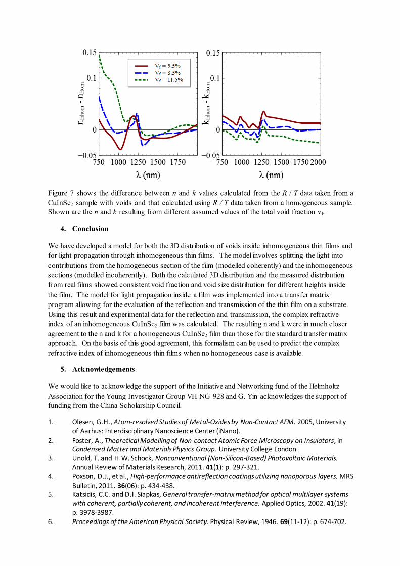
Figure 7 shows the difference between n and k values calculated from the R / T data taken from a
CuInSe2 sample with voids and that calculated using R / T data taken from a homogeneous sample.
Shown are the n and k resulting from different assumed values of the total void fraction vf.
4. Conclusion
We have developed a model for both the 3D distribution of voids inside inhomogeneous thin films and
for light propagation through inhomogeneous thin films. The model involves splitting the light into
contributions from the homogeneous section of the film (modelled coherently) and the inhomogeneous
sections (modelled incoherently). Both the calculated 3D distribution and the measured distribution
from real films showed consistent void fraction and void size distribution for different heights inside
the film. The model for light propagation inside a film was implemented into a transfer matrix
program allowing for the evaluation of the reflection and transmission of the thin film on a substrate.
Using this result and experimental data for the reflection and transmission, the complex refractive
index of an inhomogeneous CuInSe2 film was calculated. The resulting n and k were in much closer
agreement to the n and k for a homogeneous CuInSe2 film than those for the standard transfer matrix
approach. On the basis of this good agreement, this formalism can be used to predict the complex
refractive index of inhomogeneous thin films when no homogeneous case is available.
5. Acknowledgements
We would like to acknowledge the support of the Initiative and Networking fund of the Helmholtz
Association for the Young Investigator Group VH-NG-928 and G. Yin acknowledges the support of
funding from the China Scholarship Council.
1. Olesen, G.H., Atom-resolved Studies of Metal-Oxides by Non-Contact AFM. 2005, University of Aarhus: Interdisciplinary Nanoscience Center (iNano).
2. Foster, A., Theoretical Modelling of Non-contact Atomic Force Microscopy on Insulators, in Condensed Matter and Materials Physics Group. University College London.
3. Unold, T. and H.W. Schock, Nonconventional (Non-Silicon-Based) Photovoltaic Materials. Annual Review of Materials Research, 2011. 41(1): p. 297-321.
4. Poxson, D.J., et al., High-performance antireflection coatings utilizing nanoporous layers. MRS Bulletin, 2011. 36(06): p. 434-438.
5. Katsidis, C.C. and D.I. Siapkas, General transfer-matrix method for optical multilayer systems with coherent, partially coherent, and incoherent interference. Applied Optics, 2002. 41(19): p. 3978-3987.
6. Proceedings of the American Physical Society. Physical Review, 1946. 69(11-12): p. 674-702.
7. Yin, G., C. Merschjann, and M. Schmid, The effect of surface roughness on the determination of optical constants of CuInSe2 and CuGaSe2 thin films. Journal of Applied Physics, 2013. 113(21): p. 213510/1-213510/6.
8. Szczyrbowski, J., Determination of optical constants of real thin films. Journal of Physics D: Applied Physics, 1978. 11: p. 583-593.
9. Bhattacharyya, D., et al., Some aspects of surface roughness in polycrystalline thin films: optical constants and grain distribution. Vacuum, 1992. 43(12): p. 1201-1205.
10. Carniglia, C.K., Scalar Scattering Theory for Multilayer Optical Coatings. Optical Engineering, 1979. 18(2): p. 104-115.
11. Pradeep, J.A. and P. Agarwal, Determination of thickness, refractive index, and spectral scattering of an inhomogeneous thin film with rough interfaces. Journal of Applied Physics, 2010. 108(4): p. 108-117.
12. Borgogno, J.P., et al., Refractive index and inhomogeneity of thin films. Applied Optics, 1984. 23(20): p. 3567-3570.
13. Troparevsky, M.C., et al., Transfer-matrix formalism for the calculation of optical response in multilayer systems: from coherent to incoherent interference. Optics Express, 2010. 18(24): p. 24715-24721.
14. Ramanathan, K., et al., Properties of high-efficiency CuInGaSe2 thin film solar cells. Thin Solid Films, 2005. 480-481: p. 499-502.
15. Sakurai, K., et al., Properties of CuInGaSe2 solar cells based upon an improved three-stage process. Thin Solid Films, 2003. 431-432: p. 6-10.
16. Klenk, R., Chalcopyrite Solar Cells and Modules, in Transparent Conductive Zinc Oxide, K. Ellmer, A. Klein, and B. Rech, Editors. 2008, Springer Berlin Heidelberg. p. 415-437.
17. Caballero, R., et al., CGS-Thin Films Solar Cells on Transparent Back Contact Proceedings of IEEE WSPEC, 2006. Photovoltaic Energy Conversion, Conference Record of the 2006 IEEE 4th World Conference on
18. Nishiwaki, S., et al., PREPARATION OF CuGaSe2 LAYERS FOR POLYCRYSTALLINE SOLAR CELL WITH HIGH OPEN CIRCUIT VOLTAGE. Proceedings of EU PVSEC, 2001. 17th European Photovoltaic Solar Energy Conference: p. 1147-1150.