Embed Size (px)
Citation preview
A Hybrid Numerical Technique for Analysis and Design of Microwave Integrated Circuits
B.S., Tsinghua University, 1985 M.S., Tsinghua University, 1986
A Dissertation Submitted in Partial Fulfillment of the Requirements for the Degree of
DOCTOR OF PHILOSOPHY
Electrical and Computer Engineering Department
We accept this Dissertation as conforming to the required standard
0 Dr. R. Vahldieck. Sunervisor
Dr. J.'Bornemadn. Departmental Member
Dr. W. Hoefer, Departmental Member
Dr. C^Efa^ley, Outside Member
Dr. V. K. Tripathi, Exjen^l'Exanrlhen.Oregbn State Univ.)
All rights reserved. This Dissertation may not he reproduced in whole or in part by mimeograph or other means,
without the permission o f the author.
in the Department of
© Ming Yu, 1995 UNIVERSITY OF VICTORIA

Supervisor: Dr. R. Vahldieck
ABSTRACT
Miniature Hybrid Microwave Integrated Circuits (MHMIC’s) in conjunction with Mono lithic MIC’s (MMIC’s) play an important role in modem telecommunication systems. Accurate, fast and reliable analysis tools are crucial to the design of MMIC’s and MHMIC’s. The space-spectral domain approach (SSDA) is such a numerically efficient method, which combines the advantage of the one-dimensional method of lines (MoL) with that of the onedimensional spectral-domain method (SDM). In this dissertation, the basic idea of the SSDA is first introduced systematically. Then, a quasi-static deterministic variation of the SSDA is developed to analyze and design low dispersive 3-D MMIC’s and MHMIC’s. S- parameters and equivalent circuit elements for discontinuities are investigated. This includes air bridges, smooth transitions, open ends, step in width and gaps in coplanar waveguide (CPW) or microstrip type circuits. Experimental work is done to verify the simulation.
The full-wave SSDA is a more generalized and he'd theoretically exact numerical tool to model also dispersive circuits. The new concept of self-consistent hybrid boundary conditions to replace the modal source concept in the feed line is used here. In parallel, a deterministic approach is developed. Scattering parameters for some multilayered planar discontinuities including dispersion effect are calculated to validate this method.
Examiners
y --------------------------------------------------- -— — — \
fp r . R. Vahldiqck, Supervisor
Dr. J. Sfo^femann, departmental Member
Dr. W. Hoefer, Departmental Member
Dr. C. Bra$Ht?y, Outside Member
Dr. V. K. Tripathi,j2$eiHftH3Xarniner (Oregon State Univ.)
Table of Contents
Table of Contents iii
List of Figures v
List of Tables vii
Acknowledgments viii
1 Introduction I
1.1 Background and G o a ls ....................................................................................... I1.2 Organization of This Dissertation..................................................................... 7
2 The Space-Spectral Domain Approach 8
2.1 The Spectral Domain M e th o d .............................................................................82.2 The Method of Lines......................................................................................... 102.3 The Relationship Between the SDM and MoL.............................................. 142.4 The Space-Spectral Domain Approach........................................................... 16
2.4.1 SDM in x-direction......................... 172.4.2 MoL in z-direction .................................................................... 192.4.3 The Eigenvalue Solution of a Resonator Problem ............................ 25
3 The Quasi-Static SSDA 28
3.1 Why Quasi-static ? ..................... 283.2 The Quasi-static SSDA .................................................................................... 283.3 On the Nature of the S S D A ............................................................................39
4 The Full-wave SSDA 43
4.1 Eigenvalue A pproach.................... 434.2 Deterministic A pproach ................................................................................ 48

IV
5 Numerical and Experimental Results 54
5.1 Convergence Analysis of Quasi-static S S D A ............................................... 545.2 Simulation Results o f Quasi-static SSDA . . 555.3 Convergence Study o f Full-wave S S D A ........................................................ 645.4 Simulation Results o f Full-wave S S D A ........................................................ 645.5 Experimental R e s u l t s ........................................................................................67
6 Conclusion 7J
6.1 C o n tr ib u t io n s ..................................................................................................... 716.2 Future W o rk ..........................................................................................................72
Bibliography 75
Appendix 79

List of Figures
v
Figure 1.1 Example for an MMIC CircuitFigure 1.2 MHMIC discontinuitiesFigure 1.3 A typical planar discontinuityFigure 2.1 A shielded microstrip line
Figure 2.2 Cross-section view of a microstrip line
Figure 2.3 A microstrip discontinuity in a resonator enclosure
Figure 3.1 Planar circuit discontinuities
Figure 3.2 Discretization of a CPW discontinuity
Figure 3.3 The equivalent circuitFigure 3.4 A CPW Air Bridge
Figure 3.5 Configuration of general transmission lineFigure 4.1 An eigenvalue approach
Figure 4.2 A deterministic approach
Figure 5.1 Convergence analysis o f the Quasi-static SSDA (w lli= l, cr~9/>)Figure 5.2 Capacitance o f microstrip open ends.Figure 5.3 Equivalent capacitance o f a microstrip gap discontinuity. w /h=I,
h=0.508mm, er=8.875Figure 5.4 S-parameters o f a microstrip step. uq -1m m , u’2=0.2.5//////, u*//;=- /,
8 , - /0 .
Figure 5.5 Equivalent capacitance o f a CPW open e*id. er=9.6, h -■■0.6.15, /// d - l , d=w+2.s
Figure 5.6 S-parameter of a CPW airbridge. w~l5\ini,s=IO \im , l=.1\Lrn, h=200[Lm, b=1\un
Figure 5.7 S-parameters of a CPW step. w^-0,4mm, wj=0.lmm, Vj -•■0.1 mm, \\'2=0.4mm, er=9.<V, h=0.254mm
Figure 5.8 Equivalent capacitance o f a CPW gap, d { —2,Vj + it '| ,

vi
d2=2s2+u'2,£r=9.<S’, h=0.635mm, W[lh=0.2, u ’j /d 1=w2/cJ2-0.56,H'2/ir , =3
Figure 5.9 Equivalent capacitance o f a microstrip and a CPW step/taper. For CPW, W[=0.8mm, s [=0.1 mm, w2-0.2mm, s2==0.6mm, er=9.6, li=0.254mm. For microstrip, w \= lm m , w2-0 .25m m , z r=9.6, h=0.25rnm
Figure 5.10 S-parameters o f a CPW airbridge versus bridge length /. w=().3mm, s=0.1mm, b=3]im, er=9.6, h=().254mm.
Figure 5.11 Frequency dependent behavior of microstrip step
Figure 5.12 Frequency dependent behavior of CPW step
Figure 5.13 Convergency behavior o f the full-wave SSDA
Figure 5.14 Full-wave S-parameters o f a microstrip step
Figure 5.15 Full-wave S-parameters o f a microstrip step
Figure 5.16 S-parameters for a cascaded step discontinuity separated by a transmission line of length 1. w [=0.4 mm, wo=0.2m m , \\'2=0.8mm, er=3.<S\ h=0.25mm.
Figure 5.17 Measured and computed S-parameters of a CPW gap
Figure 5.18 Measured and computed S-parameters o f end-coupled CPW resonators
Figure 5.19 Measured and computed S-parameters o f a CPW step discontinu- i tv
Figure 5,20 S-parameters o f a CPW end-coupled filter. w =0.2 , s=0 ,15 , gap width: 25.4\un, resonator length: 2mm.
Figure 6.1 Future application: electro-optic modulator
Figure 6.2 An in-line 3-port discontinuity
Figure 6.3 Arbitrary multi-port discontinuity

vii
List of Tables
Table 4.1. Boundary conditions46

viii
Acknowledgments
The author wishes to express his acknowledgments to his thesis supervisor, Dr. Ruedi-
ger Vahldieck, for his guidance, encouragement and invaluable suggestions through
out the course of this thesis.
Financial support for this research by Dr. R. Vahldieck (through NSERC), Science
Council of British Columbia (through GREAT Award) and M PR Teltech Ltd. is also
gratefully acknowledged. In particular, I would like to thank Dr. J. Fikart and H.
Minkus, MPR Teltech, for the fabrication o f the MHMIC prototypes, which were used
to verify the SSDA results.
The author also wishes to extend his thanks to Dr. K. Wu for his invaluable sugges
tions. The author is also grateful to his colleagues at the Laboratory for Lightwave
Electronics, Microwave and Communications (LLiMiC), University o f Victoria for
their support and discussion.
Last, but by no means least, the author wishes to express his thanks to his family, espe
cially to his wife, Mei Li, for their support and encouragement.

I
Chapter 1
Introduction
1.1 Background and Goals
M iniaturization of microwave circuits is essential ir Mic evolution of modern com
munications systems. In analogy to the miniaturization that has taken place in VLSI (Very
Large Scale Integrated Circuits), Monolithic Microwave integrated Circuits (M M IC’s)
but also M iniature Hybrid Microwave Integrated Circuits (MHM IC’s) combine a steadily
growing number o f microwave components on smaller and smaller chip real estate.
M M IC’s as shown in Figure 1.1 [14] are very expensive in the fabrication and are only
justified for large volume applications. M HM IC’s are a hybrid technology that is in par
ticular suitable for small to medium volume applications. While M M IC’s require sem i
conductor fabrication facilities (circuits are grown on CaAs), which arc capable to
integrate active devices like FET’s (Field Effect Transistors) in one process on the same
wafer, M HM IC’s are grown on alumina substrate as shown in Figure 1.2, and active
devices are wire bonded into the chip in a final fabrication step. The latter technology is
less attractive for large volume applications because of the additional labor involves, but
offers better circuit performance and is less expensivu for small to medium applications.
Both M M IC ’s and M HM IC’s play an important role in modern communication systems.
A serious bottleneck in both technologies is the lack of accurate, fast and reliable
design strategies. Although commercial design software is available, the numerical meth
ods used are either computationally very inefficient or inaccurate at higher frequencies.
Several fabrication cycles become necessary to trim the circuit so that it satisfies the
design requirements. This process is very expensive and time-consuming (scvcra1
months). To cut dow n on the processing time and cost, it is necessary to develop accurate
design algorithms for M M IC’s and M HM IC’s in order to achieve first-pass success.

2
In generai, numerical methods can be classified into two categories:
1. Methods which use an ei genmode approach to describe the electromagneticJicld
<’ g-,
• Mode Matching Method (M M M ) 111• Spectral Domain Method (SDM) f 2 o /
2, Methods which discretize a differential operator
• Finite Difference Meihod (FDM) (6 j• Method o f Lines (MOL) [7]-[131
The first category of methods use orthogonal modes or basis functions to expand the
field directly.
The second category of methods is applied directly to either M axwell’s or the
Helmholtz equations. The first and second differential operator are approximated by
finite differences.
Both category of methods can be subdivided further into
Quasi-static techniques which calculate equivalent network parameters.
Microwave circuits are described by lumped elements like capacitors
and inductor ' . which are assumed to be constant over frequency.
Full-wave techniques which describe the electromagnetic f eld directly
from M axwell’s equations. Circuits are considered from the fie ld theory
point o f view and may be described by S-parameters, which include

3
the uite faction o f fundamental and hi»her order modes at discontinuities.
Figure 1.1 Example for an MM1C Circuit

4
COPLANARWAVCGUIDE
COPLANAR AIR BRIOCE WAVEGUIDE
SLOTLINE
(a ) C o p la n a r W avegu ide T J u n c t i o n
AIR BRIDGE
(d ) S lo t L in t C o p la n a r J u n c t i o n
air bridg e
(b ) C o p la n a r W aveguide S lo t l in e J u n c t io n
SLOTUNE
(e ) S lo t l in e T J u n c t io n
AIR BRIDGECOPLANARWAVEGUIDE
COPLANARWAVEGUIDE
AIR BRIDGE
COUPLEDSLOTLINE
MHUIC• SLOTLINE
(c) C o p la n a r W a v e g u id e /S lo t l in c T r a n s i t io n ( f ) MliMIC E m b e d d e d In to
DIODE'
AIR BRIDGE I
a CPWG S t r u c t u r e
AIR BRIDGE 3
BIAS
AIR BRIDGE 2
MIM CAPACITOR
COPtANARWAVEGUIDE
-SLOTLINE ' ' —OUTPUT
(g ) C irc u i t C o n f ig u r a t io n o f U n ip la n a r MIC B a la n c e d M u ltip lie r
Figure 1.2 MHMIC discontinuities

5
Quasi-static numerical techniques are traditionally faster than full-wave techniques,
in particular, on the serial machines widely used today. These methods do not benefit
from the availability of parallel processors. For some applications, their accuracy can
rival that o f full wave techniques and, therefore, they arc very useful engineering design
tools.
Theoretically speaking, a quasi-static approach only works at zero frequency. How
ever, as long as the dimensions of circuits are small compared with the wavelength and
the dispersion of the transmission line system is weak or non-existing, quasi-static meth
ods cun work up to the millimeter-wave range. A large number of commercially avail
able software is built on quasi-static methods. In most cases the equivalent element
values derived from quasi-static methods are assumed to be constant over the frequency.
Furthermore, it is assumed that the discontinu,ties for which they are derived do not radi
ate or interfere with each other. This assumption becomes invalid the closer microwave
elements are placed on the chip. In this case the predicted performance of the M M IC’s or
M HM IC’s may deviate significantly from the required performance.
For structures, or frequencies, at which quasi-static methods do not provide accurate
results, either because the circuit density is too high or dispersion effects arc too signifi
cant, full-wave modelling of microwave and millimeter-wave circuits becomes neces
sary. In this dissertation, a generalized Space-Spectral Domain Approach is first
introduced that is suitable for this task. Secondly, a new quasi-static deterministic tech
nique will be presented. Finally, two SSDA full-wave algorithms will be discussed.
Typical generalized full-v/a -e approaches are, e.g., the Finite Difference Method
(FDM) or Transmission Line Matrix (TLM) fl6 j method. These methods start directly
from M axw ell’s equations with very little approximation and virtually no analytical pre
processing. They have almost no structural limitations and provide a high degree o f accu
racy. Being very flexible, they often require large amounts o f computer memory and long
computer run-time, at least on most of today’s available engineering workstations. To
speed these methods up, parallel processor machines are required which, for some time
to come, will not be commonly used in engineering laboratories because of the special
program languages necessary to fully take advantage of the potential of these machines.

6
side view
top view
▼ x
Figure 1.3 A typical planar discontinuity
When dealing with the analysis and design of M M IC ’s and M H M iC’s, their quasi-
pJanar structure, as shown in Figure 1.3, allows the use o f less generalized but computa
tionally more efficient techniques. In the past, the most suitable methods for 3-D planar
circuit analysis have been the Spectral Domain M ethod (SDM), the Mode M atching
Method (MMM), and the M ethod of Lines (MoL) (full-wave and quasi-static).
In the SDM, the Fourier transform is taken along a direction parallel to the sub
strate, and G alerkin’s teetmique is used to yield a homogeneous system of equations. To
determine the eigenvalue problem (propagation constant) in a planar circuit, the 1-D
SDM is well known for its fast computational algorithm and minimum memory require
ments. But the SDM also requires that the circuit discontinuities fit into an orthogonal
coordinate system and, especially, that the basis functions are chosen carefully. For 3-D
discontinuity analysis, the 2-D SDM requires usually a large number of two-dimensional
basis functions which are not easy to chose and handle and which increase the computa
tion time significantly because o f potential convergence problems [43].
The MoL is a space-frequertcy domain method similar to the FDM but uses an
orthogonal transform. To treat 3-D discontinuities, the 2-D MoL is used, which dis
cretizes the two spatial variables parallel to the substrate plane while an analytical solu
tion is obtained in the direction perpendicular to the substrate plane. This method
requires only a two-dimensional discretization for a general 3-D problem. The advantage
of this method is its easy formulation, simple convergence behavior and the fact that there
are no special basis functions necessary. The disadvantages of the 2-D MoL is that satis

7
fying all boundary conditions simultaneously for arbitrarily shaped circuits may be very
difficult or may require a very fine 2-D discretization. In short, when applying the SDM
or MoL to an arbitrary 3-D discontinuity problem, each method by itself encounters a
number o f serious problems which are inherent in the method.
To overcome the inherent limitation of each method, a new hybrid numerical
method has been developed by Wu and Vahldieck fl7]. This method is called the Space-
Spectral Domain Approach (SSDA) which combines the 1-D SDM and 1-D MoL. This
new m ethod eliminates the shortcomings of the conventional 2-D MoL and 2-D SDM and
takes advantage o f the attractive features associated with the 1-D SDM and the 1-D
MoL. The SSDA is developed in particular for the analysis of arbitrarily shaped spatial 3-
D planar discontinuities.
In this dissertation, we first introduce the generalized SSDA concept which is
extended from the work of Wu and Vahldieck [17], Although this analysis can only be
applied to calculate resonant frequencies but not discontinuity S-paramctcrs, it is used to
explain the basic idea of the SSDA. On that basis, a new deterministic quasi-static SSDA
[18], [20] is presented followed by a full-wave SSDA [19], which is aimed at the calcula
tion of S-parameters in structures supporting hybrid modes.
1.2 Organization of This Dissertation
Chapter 2 reviews the SDA and M oL and investigates their relationship, which
forms the basis o f the SSDA. The generalized SSDA is introduced in a planar resonator
problem which forms the basis o': this dissertation.
Chapter 3 introduces the quasi-static SSDA.
Chapter 4 introduces the full-wave SSDA.
Chapter 5 discusses simulation results and their experimental verification.
Chapter 6 concludes the dissertation.

Chapter 2
The Space-Spectral Domain Approach
In this chapter, the Spectral Domain M ethod (SDM), the Method o f Lines (MoL) as well
as the relationship between both m ethods are first reviewed. The concept o f the Space-
Spectral Domain Approach (SSDA) is introduced as a com bination o f the SDM and the
MoL. For a three-dimensional (3-D) electrom agnetic problem, the SDM is applied to the
x-direction, the M oL is applied to the z-direction, and the analytical process is applied to
the y-direction (see Figure 2.1).
Figure 2.1 is a 3-D version of Figure 1.3; it shows a typical planar circuit discontinuity in
a shielded box. In the Spectral Domain M ethod the Fourier transform is taken along the
x-direction for a 2-D problem and always along the x- and z-direction for a 3-D problem.
The analysis in the Fourier transform dom ain was first introduced by Yamashita and M it-
tra [2] for com puta tion of the charac te ris tic im pedance and the phase velocity o f a
microstrip line based on a quasi-static approach. It is one of the m ost popular and widely
used numerical techniques for planar circuits. Numerous publications can be found in the
literature, e.g., [ 3 -5 ] .
For planar transmission line and discontinuity problems, the electric and magnetic
fields E and /? are often written in terms o f scalar potentials and ¥ 1 in a Cartesian
coordinate system, shown in Figure 2 .1 (this is called a TEZ / TM Z formulation)
2.1 The Spectral Domain Method
VxVxl 4 'c(2. 1)

where z is the unit vector in z-direction. h satisfy the wave equation
- j2 e , h ^ 2 c, h 0 2 (-,/!
+ L- ~ - + - • „ + k 'V ’ = 03.v 3 A 3r
, 2 2 k = CO (0.8
(2 .2 )
A y
/
Figure 2.1 A shielded microstrip line
The idea o f the SDM is to apply the Fourier transform along the x-diicction in
order to eliminate the space variable x and replace it with a spectral term a x
e, h c h j a x . y = f M' c dx (2.3)
Assuming the problem is a two-dimensional one in x- and v-dircction, with the
propagation constant p in z-direction, equation (2.2) yields
-,2 e, h2 e ,h a \u _ 2 e,/i ,2 e ,h _a y + — — P ij/ + k i|/ = 0
3y(2.4)
The above equation (2.4) can be further simplified as a one-dimensional normal dif-

10
ferential equation
2 r 2 2) _ a + (3 - A' I q/ = 0 (2.5)
By applying the boundary conditions (more details will be given in Section 2.4 ),
one finally obtains an algebraic equation in matrix form
e and e. are the Fourier transforms of the electrical field in the a - and r-direction.
/ and /\ are the Fourier transforms of the current in the a - and r-direction. The unknown
/ ( and / are expanded in terms of known basis functions with unknown weighting coeffi
cients. By applying G alerkin’s technique, the propagation constant and field distribution
can be found.
In summary, the SDM has several features:
• Simple form ulation in the form of algebraic equations• Utilization o f a-priori (physical) knowledge of modes• Numerically efficient
The SDM is well known for its computational efficiency and minimum memory
requirement for two-dimensional problems (1-D SDM) because usually only a few basis
functions are needed. The SDM loses some of its advantages when applied to spatial
three-dimensional discontinuities (2-D SDM). In particular when these discontinuities
are arbitrarily shaped, it becomes generally a problem to find suitable basis functions and
to achieve reasonable convergence.
differential equations. It was applied to m icrow ave analysis and design problem s by
Pregla and co-authors [8 - 13].
The concept o f the M oL is as follows: for a given system of partial differential
(2 .6)
2.2 The Method of Lines
The Method of Lines (MoL) was first developed by mathematicians (7 J in order to solve

I t
equations, all but one of the independent variables are discretized to obtain a system of
ordinary differential equations so that the whole space is represented by a r umber of
lines. This semi-analytical procedure is very useful in the calculation o f planar transmis
sion line structures.
To demonstrate the basic steps of the MoL, consider the microstrip line cross-sec
tion in Figure 2.2
x=L
Figure 2.2 Cross-section view of a microstrip line
Equation (2.2) is to be solved here. The discretization is done in the .v-direction as
shown above. The figure also shows that two separate line systems are used to represent£1 /i
lP and T . This shifting scheme has several advantages: the lateral boundary condi
tions are easily fulfilled, it allows an optimal edge condition flOj, second order accuracy
[11] and simple matrix formulation.
Let the number o f ¥* and xVn lines in Figure 2.2 be equal to Ari, The potentials on
all the lines are combined to form a vector ^ and respectively. Equation (2.2) can
then be rewritten as
(2.7)-.2 r A t J l . .2 rA f j l .
+ L ^ _ + t V * = 0dx dy dz
The first derivative with respect to x is formed as backward difference quotients for
'V1 and forward difference quotients for XV"

12
d*P' r —' • o a r ^ N 11'
>/J (2.8)
with
£> =
1 ... 0 0 -1 ... 0 ... 10 ... 0 -1
(2.9)
In the difference operator [D] the lateral boundary conditions are included (here a
Dirichlet-Neumann boundary condition is used as an example). The second derivatives
can also be represented by means of the operator [D]
h232^
OAD
. 202T>/' a o T T ^ "ox
Equation (2.7) can then be written as
xx
DhXX
(2. 10)
32$ ’ ( - 2 _2 ;2W
dy(2.11)
where
" = h (2. 12)

c ,h is the eigenvalue matrix and 7 , c , h the eigenvector belonging to h whichcan be obtained analytically dependent on the different lateral boundary conditions 1111.
For example, for the structure shown in Figure 2.2, the elements of arc
~,e . in n7 ‘." = s,n/v7 T N (2.14)
Equation (2.12) is called the orthogonal transform because rf-n is a symmetrical
matrix and f ' is an orthogonal matrix. Equation (2 .11) is in the transform domain,
which is similar to equation (2.5) in the Fourier domain. However, the way to solve equa
tion (2.5) and equation (2.11) are different in either techniques. By applying lateral
boundary conditions, a system equation similar to equation (2.6) can be obtained. Apply
ing the orthogonal transform a new algebraic system equation can be derived in the (orig
inal) spatial domain ([11] gives more details)
(2.15)
The vector notation is used here to represent discretized quantities. Because equa
tion (2.15) is in the spatial domain, it can be simplified by removing those lines which do
not pass through the metallization at the interface
0 = Z.I ,
(2 . 16)
The propagation constant and field distribution can be calculated by solving the
root o f the determinant of jzf] , where subscript r signifies that [Zr \ is a residual matrix.
For three-dimensional problems also the z-variblc is discretized (2-D fvloL).

14
In summary, the 1-D MoL has the following features:
• No basis function needed• Simple formulation and efficient calculation• No relative convergence phenomenon
However, similar to the SDM, when applied to three-dimensional problems, the 2-
D M oL becomes numerically less efficient because of the two-dimensional discretization.
2.3 The Relationship Eetween the SDM and MoL
From the previous sections, it is quite obvious that both methods, the SDM and M oL,
have som e sim ilarities if one com pares equations (2 .3), (2.5) and equations (2.11),
(2.12). The following analysis shows that the MoL is indeed related to the SDM and that
this relationship helps to combine the advantages of both m< ‘hods into one new method, the Space-Spectral Domain Approach.
This becomes obvious if one rewrites equation (2.2) for the two-dimensional trans
mission line problem (the superscripts of T are removed without loss of generality)
^ + = 0 (2.17)dx2 ay 2 y
where (3 is the propagation constant.
In both the MoL and SDM, a transformation is performed in the .v-direction
MoL ¥ = > $ # = > $ $ = [7] $
(2.18)SDM 4' => \]f fg = J
.00
which leads to a onc-dimensional normal differential equation that corresponds to
equation (2.5) and equation (2.11).
From equation (2.18) one may deduce that the orthogonal transform in the MoL
represents a discrete Fourier transform in matrix form. Although in [11J some analysis is
provided to support this point, there is no clear explanation to prove that the M oL

scheme (discretization and orthogonal transform) and the SDM are truly identical. Fur
thermore, also the connection between the SDM, the MoL and the SSDA has not been
investigated in detail. The following analysis is intended to fill this gap.
To demonstrate the relationship between the SDM and the MoL, the structure in
Figure 2.2 is used again. (Dirichlet boundary condition is applied for the electric potcn-Q
tial T at a - ( ) and at x=L ) The Fourier expansion in region [ 0 , /.] is written as
L
V = jT ^ s in axeLx 0
a =in/- (2.19)
/ = : - D O or
If the potential is discretized into N points in the x-direction, i.e.
nn N . + 1
L , / '= / N:, and N: spectral terms are used,
N.e . inn
sin-ii = i
N + 1/ = I N_ (2 .20)
The subscripts are used to represent discrete quantities and discrete spectral terms.
If vectors are used to represent discretization, equation (2.20) can be rewritten as
\\i =
where the element of J ' Jn e . inn
From here one may compare
M oL
SDA .if r "\U = I rV!^ I.1 J
t ] ' / ’
(2 .2 1 )
(2.22)
(2.23)
From equation (2.14)

16
This shows that the MoL is a discrete SDM. The equivalence o f the MoL and the
SDM is established under the same finite discretization scheme. From another point o f
view, because the SDM (theoretically) uses an infinite number of spectral terms, the
SDM gives an infinite number of precise eigenvalues and eigenfunctions which can be
solved using analytical transforms while the MoL yields a finite number of approximate
eigenvalues and eigenfunctions which can be solved using finite discretization.
In summary the following properties are found comparing the SDM and M oL
• The SDM and MoL are indeed related to each other.
• Both o f them are numerically very efficient for 2-D problems and less efficient for 3-D problems.
Combining the MoL and SDM will take the advantage o f both methods to analyze
3-D problems more efficiently. This leads to the invention o f a new method called the
Space-Spectral Domain Approach (SSDA).
2.4 The Space-Spectral Domain Approach
This section describes the basic p rinc ip les o f the Space-S pectra l D om ain A pproach
(SSDA). The SSDA was first introduced by Wu and Vahldieck f 17] and further developed
by the author together with Wu and Vahldieck [18 - 20]. First, a generalized introduction
is given for a 3-D planar resonator circuit.
The two techniques combined in the SSDA are the SD M to simulate the cross sec
tion of transmission line structures and the MoL to model their longitudinal direction.
The microstrip line step discontinuity shown in Figure 2.3 is taken as an example to dem
onstrate the basic steps involved, n this chapter only the hom ogenous boundary condition
is considered (the discontinuity is enclosed in a shielding box).
First o f all a combination of electric and magnetic lines are introduced to discretize
the structure in the z-direction. This corresponds to slicing the structure in the x-y plane.
Then a set of conventional basis functions for each slice is introduced which satisfy the
boundary conditions along the x-coordinate. Every slice is o f regular rectangular shape,
so that only well known conventional 1-D basis functions are needed. The Fourier trans
form is performed to replace the x-coordinate in the Helmholtz equation with the spectral

17
term u . Since the M oL procedure is used in z-direction, the resulting wave equations arc
coupled. The orthogonal transform in the spatial domain is utilized to decouple the sys
tem equations. The three spatial variables in the Helmholtz equation are now reduced to
the remaining y variables and can therefore be solved analytically. The advantage of this
procedure is that fine circuit details such as narrow strips and slots as well as compli
cated discontinuity shapes can be easily resolved by discretizing the structure in z-direc
tion. Furthermore, problems such as complicated basis functions, huge memory space and
long CPU time known from the 2-D SDM or MoL (i.e. 3-D problems) are avoided. The
final steps o f the SSDA are: the boundary conditions between layers at the top and bottom
of the closed structure are transformed into the circuit plane. Satisfying the boundary con
ditions at that location leads to a set of equations which are the Green’s functions by
nature. A fter transforming these final equations into the spatial domain, Galerkin’s tech
nique is applied so that a characteristic matrix equation is obtained. By introducing
hybrid boundary conditions, the S-parameters can be obtained. This will be discussed in Chapter 4.
2.4.1 SDM in x-direction
The cross-sec tion o f a m icrostrip resonator is shown in Figure 2,3, Although a single
layer structure is draw n for the purpose o f simplicity, the following formulations are also
valid for a m ultilayer structure (yk and ym are used here for a generalized formulation).
The electrom agnetic field in the p 'h layer can be expressed in terms o f scalar potential
functions accoraing to equation (2.1)
VxVx T i
(2.25)

18
t1
2e rr
M/ '
>[/'
I its
y=y«
y=yn
x=a
‘hi
Figure 2.3 A microstrip discontinuity in a resonator enclosure
V* and H!1' are the solutions of the partial differential Helmholtz equation pair
L 2 L _ + L 3L _ + L 3L _ + ^ . y ‘ = 0O.v dv d : (2.26)
*o = to V e 0
where
ppr is the relative dielectric constant in the plh layer. The Fourier transform is

19
applied in .v-direction
. . . c , / / c, h(2.27)
CO
h r n , f ’, h j a x ,V = J 1 e dx (2,28)
_00
where a is the space-spectral variable.
The electric and magnetic field vectors in equation (2.25) will take the following form in the spectral domain
00 COr ^ j a x , -j-
e =_oo
J E c ^ d x J = J E e ^ d x (2.2.9)
The space-spectral domain Helmholtz equation can now be written as:
32q/e,/l d2y L' h ( 2 / j ,2'') (Uh~ 7 T - + - T r - 1 a - r oJ = 0 (2-30)
dv oz
2.4.2 MoL in z-direction
After the Fourier transform has been applied in .v-direction, the M ethod of Lines (MoL)
can be applied in z-direction. The structure is sliced in the x-y plane at each r-coordinatc.
The electric lines and m agnetic lines are introduced to represent the discretized scalar
potentials in the spatial Fourier transform domain. A total num ber o f AL lines are used
for different types o f transmission line configuration.
In vector notation the discretized potentials v ^ ' are written as a N .-element vector
as described in Section 2.2 .
\ \ h \pc' 11 (2.31)
Non-equidistant discretization [15] can be used here to increase the flexibility. The
non-equidistant discretization can also be considered as a linear transform from
(original vector) to cp4’ 1 (non-equidistantdiscretized vector)

_s. <\ h hX|/ —> cp
20
(2.32)
^ Q JjThe new potential cp ’ is defined as
h<P v
h(2.33)
where
re,h = diag (J;MI A/ >le< hi)
(2.34)
he lli denotes the discretization interval of electric and magnetic lines, respectively.
h() is the limiting case for the discretization interval (equidistant discretization).
The finite difference expression of the first derivative is written in matrix notation
where
. 3(p‘
. a?"
D.
D.
D.
<P
<P
(2.35)
(2.36)
[D] is defined in equation (2.9). The second order derivatives can be written as
D_
D
<P
<P
(2.37)
where
D. D. D. D D. D. (2.38)
Because [/T is a symmetrical matrix, the following transforms can be applied

to transform this matrix into a diagonal form:
h,
i r vT c
od : 7 = 6ce 2
ll0T 7 = 52
21
(2.39)
Similar to Section 2.2 , a new potential in the (orthogonal) transform domain is defined as
s. <\ //TA h <P
.A /l(2.40)
The final 1-D Helmholtz equations in the transformation domain are derived from equation (2.30)
a v
d v 2
d2^ f .2 2 2) /,~ ~ 2 \ Ith + CX - £r ko ) V = 0 dv
(2.41)
The analytical solutions o f the above N, decoupled equations can be expressed as
transmission line equations from point ym to y k. The /^'component is
V*I
dV:
V,.
coshy .d. - sinhy del i yei- 1,1 i
yel.sinhy cid. coshy eid.
V,
dV,
. d y . .
(2.42)
where
a /= coshM ^ /usinhM
/dy
Y/(,-sinhy/((.d. coshy/(/d.
V
dVdy.
(2.43)
2 £ 2 2 p . 2yei, = 6„ + a - B rkQ
2 2 2 „ 2 y>ih = 6/ ,/ ,+ a - e/ o
d l = (2.44)

22
The equation (2.42) and (2.43) can also be represented in matrix form as:
r p e
b p " BPBy
BPe=
Y p.By
BP"By By^ h 1/ _ h V
(2.45)
where [Qp] is a 4N: by 4N2 matrix
\P p.
Ce L°J ^
c, 3h2
M [o] H [o]
[o] M [o]
(2.46)
= d iag (coshy .d.)
Sel = d iag ( sinh (y(,.t/(.) / y j
C,
’/ii
3 cl = d iag (y^sinh (ye|.d .)) h 2
= diag (coshyh.d.)
= diag ( sinh ( y/( .</.) / y /|(.) (2.47)
= diag (y,„.sinh (y/l/r//) )
If one uses ex, ez and hx, hz to represent the components of e and Ti defined in equa
tion (2.29), then from equation (2.1), the transverse electromagnetic field in the p ll‘ layer
can be expressed in the spectral domain as
_ a d\yc d\\rh _. _ a By" ^ lx ~ By + mp0 dz
e , =j(£>£0£Pr
(oeQePr d : dy
' S 2 <a \v i> .2 e — T + e, k oV j th cop
( -a h N
V s -V d z /
(2.48)

23
Applying the non-equidistant discretization, equation (2.33), and the orthogonal
transform, equation (2.40), the fields in the transform domain can be written in matrix
notation as
where
b = -a b _dP'
toe0er dv
P 1,2 y-
$ = ££pe. P
j a>£0£r
- I =dP_
' 3va 5, y -copn
J l =
J', . 2 *r 0 ~ °/j /i f / 1
00(X
t = jjl _rh_ K 1 =I
- 1
1
r ,
b =~z f . k = 7J[- 1 r' h
-I
(2.49)
(2.50)
Note that the vector formulation is introduced to represent the MoL discretization.
Using block matrix notation
ihz
- L
R,
f
dPhdydP"dya /'
(2.51)
where [R/;] is a 4NZ by 4NZ matrix

24
R.
a b l,ep
t o e 0 £ r-0 [o] [o]
P . 2 j, r 0 " ee
j<oeQePr [o] [o] [o]
0 [o] [o] - 6 cop.
[o] [°] -[/] a 5 ,/l
c o p 0
(2.52)
By combining equation (2.45) and equation (2.51), the field relationship between two layers is
J t .
- L
LR P_ f i p jR.
'h
jljz
- h x
(2.53)
Tli'* expression for m ultiple layers can be obtained by cascading the respective matrices.
With equation (2.53) one can always transform the electromagnetic field from one
layer another. By transforming fields into the layers o f metallization arid applying the
boundary conditions at those interfaces, a matrix equation similar to equation (2 .6) and equation (2.15) can be obtained
\e~,v n lx
= Zb~z
LX! \Lk
(2.54)
[zj ‘s a ^ ’z by 4M, matrix. Transforming the electric fields and currents back into
the original domain by using the same orthogonal transform introduced in equation
(2,40), the spectral domain algebraic matrix equation becomes

25
\
JxX= TzlI / d \
Jz
where [Z] is a 2NZ by 2/V, matrix
[z] => 1 [o ]
T
-l
(2.55)
[o]
tTC1 r 1-1
(2.56)
In summary, the following transforms have been utilized in the above analysis
—> Fourier transform -> non-equidistant discretization —> orthogonal transform
i.e.
(2.57)
( Ex .y - > ex,y) (Zx,y->2jc.y)
( JX, V j'x, y ) ( a - , .V - * I
The system equation (2.55) is obtained by following the reverse procedure.
In summary, equation (2.1) to (2.57) represent the generalized procedure of the
Space (from the MoL)-Spectral Domain, (from the SDM) Approach (SSDA). Although in
this chapter, the formulation is limited to a resonator problem, the foundation o f the
SSDA for scattering parameter calculation, which will be discussed in Chapter 3 and Chapter 4, is laid.
2.4.3 The Eigenvalue Solution of a Resonator Problem
The resonant frequency of a planar resonator can be calculated by finding the roots o f the determinant o f the system equation [17 ].
G alerkin’s technique is applied to obtain the chaiactcristic matrix equations. The

26
first step is to expand the elements o f unknown j x and /_ in terms of known basis func
tions with unknown coefficients a . and a[.
N ,/ /
N - 1/ /
h i = £ a x i X\x i h i = Z /= 1 / = 0
(2.58)
where / represents the /th basis function, Nx is the total number o f basis functions, / repre
sents the /th line and
-ah
(2.59)
where >t>;- is the strip width. J0 is the 0tn order Bessel’s function. Or, in vector notation
1 /■n,I
n"ipr
/ /'H.wv, V
(2.60)
Calculating the inner product between basis functions and each element of the sys
tem equation (2.55) (further details can be found in Chapter 3) yields
fK ' < d a = f da (2.61)
the right side o f equation (2.61) is always zero. The left side can be written as
!/■ '(/)]* = 0 (2.62)
*s the result of the inner product and cl represents the coefficient vector, f
denotes the resonance frequency which can be obtained by solving the zeros o f the determinant
d e ( ( /• '( /> ]] = 0 (2.63)

27
To extend the SSDA to calculate the S-parametcrs o f planar discontinuities the
deterministic quasi-static SSDA and the full-wave SSDA with hybrid boundary conditions are introduced in Chapter 4 and 5, respectively.
28
Chapter 3
The Quasi-Static SSDA
3.1 Why Quasi-static ?
Q uasi-static numerical techniques are traditionally faster than fu ll-w ave techniques in
particular on the serial machines widely used today. These m ethods do not benefit from
the availability of parallel processors. For some applications their accuracy can rival that
o f full-wave techniques and, therefore, they are very useful engineering analysis tools. In
the recent literature, the quasi-static analysis has again received more attention [21 - 24],
because M M IC’s and M KM IC’s are usually small in dimension com pared with the oper
ating wavelength and, therefore, dispersion is normally weak. In [21] a quasi-static spec
tral dom ain approach (SDA) was used to ca lcu la te m icrostrip d isc o n tin u itie s . T his
m ethod is num erically efficient but requires com plicated 2-D basis functions, w hich
som etim es may be difficult to find. A quasi-sta tic finite d ifference m ethod (FD M ) is
described in [22] to analyze CPW discontinuities. This method can treat arbitrary discon
tinuities, but at the expense of large computer memory. In [23] the quasi-static method o f
lines (M oL) is employed to analyze cross-coupled planar m ulticonductor system s. This
method does not use basis functions and is faster than the FDM but still requires signifi
cant amounts of memory and is difficult to apply to arbitrary d iscontinuities. The deter
ministic SSDA eliminates these problems and will be introduced in the next section.
3.2 The Quasi-static SSDA
This approach utilizes the basic idea behind the SSDA but avoids solving an eigenvalue
problem by using a new deterministic technique instead. To minimize errors in the calcu
lation of the capacitance parameters, the excess charge density [24] has been used and
calculated in the space-spectral domain in one step via Galerkin’s m ethod. This approach

29
leads to an algebraic equation for the equivalent circuit parameters o f the discontinuities and is computationally very stable, requires little memory space and is very fast on serial
computers. This method is capable of treating arbitrarily shaped planar circuit discontinu
ities. Figure 3.1 illustrates the type of discontinuities this method has been applied to.
Microstrip Open End
Microstrip Gap
Microstrip Step
CPW Step
■.vfSSKtSTIS*?.;?CPW Open End
CPW Gap CPW Air Bridge
Figure 3.1 Planar circuit discontinuities
CPW Tai c
I T T S Z 3
VMicrosirip Taper
A CPW discontinuity illustrated in Figure 3.2 is used as an example to demonstrate
the theory. This discontinuity contains three regions (1, 2, 3) with thicknesses It/, It,, hi and is shielded by a metal housing. The three regions arc defined as:
1. hj+li2<y<h]+h2+ht2. hj<,y<ch i+hi3. 0<y<hj
As mentioned before, discretization of the structure in z-direction corresponds to
slicing the structure in the x-y plane at each z-coordinatc. Therefore, the potential for
each slice must satisfy the 3-D Laplace’s equation
)2 I 2 )2J L y + J L v + J L v = o ( 3 I )r).v 0 y 2 r):
In this case k=() (o>=0, compared with equation (2.2)). The task here is to simplify
Laplace’s equation which depends on the three spatial variables. The electric lines (solid
lines) are introduced to represent a discretized electric potential ip, which is independent

30
of the magnetic potential. The dashed lines are used to represent the m agnetic potentials
as used in the conventional M oL (the magnetic potential is not o f interest here because it
is independent of the quasi-static electric field). The shift in both lines is necessary to
reduce the discretization error and can be derived from [8]. Similar to Chapter 2, the first
step is to transform the electric potential function 'F into via a Fourier transform
along the x-direction. Here the superscript is omitted because only the electric potential
is of interest. The spatial variable x becomes a spectral variable a . The next step is to
discretize \(/ by using Nz lines in the z-direction which leads to the vector \p. The
tapered region is enlarged in the left part of Figure 3.2, which demonstrates how a smooth
transition is theoretically discretized and approximated by a sequence of abrupt steps.
Top ViewCross Section
Enlarged discontinuity
m-line
e-line
Figure 3.2 Discretization of a CPW discontinuity
By utilizing the basic steps of the SSDA in Chapter 2 with non-equidistant discreti
zation in the z-direction, Laplace’s equation can be decoupled
^ - j - y 2 P = 0 (3 .2 )dy
where

31
2 _2 2 y = o + a I']* (3.3)
Due to the discretization, Laplace’s equation (3.1.) is now reduced to only one spa
tial variable, y. 5 is the eigenvalue o f D ,, . ['/’] is the eigenvector matrix. 6 and |y j
are defined in Chapter 2 (note: the superscript e is omitted here because only electric
potentials are used in the formulation, y has only two terms instead of three as in Chap
ter 2 because k=0). Solutions to the above 1-D simplified Laplace’s equation can be
expressed in terms of the sum o f hyperbolic functions, and the relationship of the electric
potentials between any two adjacent layers can be expressed in the same way as
described in equation (2.42) o f Chapter 2, that -s
XdV, —
dy V*
coshy .d - sinhy.J1 i yi ' i
y .sinhy^ , coshy(c/(
I-',()\\c)v
(3.4)
V, is the ilh element of P and corresponds to the ilh line of discretization. Because
equation (3.2) is decoupled, each line is represented by the same form of normal differen
tial equation. Without loss o f generality the subscript / can be removed in the following
analysis. Instead, the subscript is now used to represent the potential in the different dielectric region.
For Laplace’s equation, there is always y = y, = y2 = y.? because k„ 0 in equa
tion (2.43).
The boundary condition at the interface is as follows:
atat
y = l>2 + ^h
v = h .j(3.5)
31/, Sv2£ , - ^ E 0 -=— - — L
-'2 dv
dV2
"2 3v 5 dy
at
at
y = h2 -f //3(3.6)
where q is the charge density in the transform domain. At the top and bottom m etallization

32
V{ = 0 at v = h { + h2 + /i3
V3 = 0 at v = 0
Substitute equation (3.7) into equation (3.4) yields
dV~ Ydy tanh y h2
dV3 _ ydy tanh y/i3 ' 3
Combine equation (3.4) - (3.8) provides
8(y) Vi
at
v = h2 + /i3
v = h-.
(3.7)
(3.8)
(3.9)
where
S(Y) =c 2y
+e iY
£2y
tanhy/i2tanhy/t2 tanhy/i, e2y e3y
tanhy/i2 tanhy/?3
(3.10)
To characterize a discontinuity, one needs to find the solution for the electric charge
belonging to the discontinuity part. This is usually achieved by subtracting the total
charge o f the discontinuity area and the charge belonging to the connected transmission
line. Since both quantities are often quite small, the errors arising from the subtraction of
two electric charges, which are close in magnitude, can be significant. To avoid these
errors, the excess charge technique [24] is used. This technique can briefly be summa
rized as follows; the 2-D transmission line problem is solved first in the spectral domain
on either side of the discontinuity, i.e. solving equation (3.2) (homogeneous transmission
line in z-direction) and analytically subtracting the charge distribution of the fictitious
homogeneous transmission line from the charge distribution of the corresponding discret
ization line o f the transmission line containing the discontinuity. Based on the above for
mulation, the 2-D problem can be solved by using the solution given in equation (3.9)
with 5 = 0 , i.e. y = a
K (oc)l', = ~ £ .
33
(3.U)
wnere <■/„ is the charge density o f a fictitious homogeneous transmission line. The
excess charge density p is defined as
( 3 .1 2 )
Now the excess charge technique is applied, which means the two quantities g(y) and g(a) are subtracted
= U (Y ) - A'( « ) ) l~ ( 3 .1 3 )
and the results are transformed back into the original domain
M' = C P
a is the excess charge vector in the original domain and
H = H H Mag [g (y) - q (a)] ‘ ’‘ [?J'
(3.14)
( 3 .1 5 )
where diag[g(y)-g(a)l includes the difference [g(y)-g(a)J from all the lines. The size o f the matrix is Nz by N z.
G alerkin’s technique is now applied to obtain the characteristic matrix •equation.
The first step is to expand the elements of the unknown a in terms of known basis func
tions with unknown coefficients c/
a = I I( 3 .1 6 )
where Nx is the number of basis functions, N, is the num ber o f discrete lines and
1 r J j a x j4 , = | V dx ( 3 .1 7 )

34
T|/ and <5/ are Fourier transform pairs of basis functions. For CPW circuits, they
take on the follow ing form for the center conductor with width ivj (also for microstrip cir
cuits with width i»’j)
cos ( 2 1 - 1) tc-I.
I = 1, 2 , (3.18)
nu'j•n, = - r
a w . \ ( aw ./ = 1 ,2 , . . . (3.19)
For (CPW ) ground (symmetrical) conductors (iv/( is the ground conductor width, is
the x-coordinate o f the ground conductor center (one side))
cos In-( x + b w!)
w ucos In
( x - b .)v 117'H ’ i /
II -
Sill
2 ( x + bwt)
w i 1 J x < 0
(x + b J/ tc -
IV 1/
1 -
sin
n x + b j
w u J .v> 0
(x ~ bJIn-" ’u
11-2 (X + ! U )
\ w u J11 -
IV ,
x < 0n /
.v>0
I = 0 , 2 , . . .
/ = 1,3,
(3.20)
J n w " ,11/ = — x - c o s a b wi
11/ = s in a 6w/a iv 1(. - I n
I = 0 , 2 , . . .
/ = 1,3, ...
(3.21)
For different microstrip or CPW discontinuities, one only needs to adjust ivp b wi

and w u of each line instead of changing the form of the basis function. Thus the disconti
nuity shape can be arb itrary . This is an advantage of the SSDA and makes it possible to develop contour driven software.
Similar to Chapter 2, the inner product between basis functions and each element of the system equation (3.14) is calculated
/ = 1 ,2 N . (3.22)
In quasi-static analysis, the excitation potential is always a constant across the met
allization. This property can be utilized to achieve a simple deterministic solution
through the use o f Parseval’s theorem
J tj/ • 'q ^ a = 2 k J lF • t; clx (3.23)
where
1' =
\1!
IV 1 k
(3.24)
'F is the discretized electric potential (inverse Fourier transform of ij/) and is con
stant across the metallization. If this constant is defined as V' , the left side of equation
(3.22), which is further processed in equation (3.23), can be written as
J m> • n d a = 2u V (, | % dx = 2nV tj \ I « = 0 (3.25)
Unlike the full-wave resonator analysis described in Chapter 2, the left side o f sys
tem Equation (3.22) is known as an • gebraic equation. The deterministic solution can be
obtained by matrix inversion. Rewiiting equation (3.22) in matrix form, which contains
Nx independent equations, will yield

36
2 nV ,A,
- Ja = 0
[c]® J ’1d a (3.26)
By using equation (3.16) and replacing the continuous integral by a discrete sum
mation, equation (3.26) can be written as
(3.27)
where
Aoc Z| = Block (3.28)
a = 0
km
1 1 2 *
i 2 2 2
Nx 1
G k m % n T1/n
^ 2 G k m X S m (3.29)
/v. A„ Nx N,^kni ^n t ^m ^ k m ^ m ^ m ^k n t^ m ^
A a is the step width of the discrete Fourier integration. [Z] is a ,V_/Vr by N:N y. block
matrix, which contains Nz by Nz submatrices. Each submatrix fZ ]^ , is a Nx by Nx
matrix. G \m is the (k, m) element of [G],
The charge density coefficient vector d is defined as
d = 1 2 <i a L . .
Nx 1 2*2 Cl7
A. 1 2 A.ClNz V - "A’ (3.30)
Front equation (3.27), it is evident that only a one step matrix inversion is now required

37
(3.31)
In contrast to finding zeros of a determinant through an iterative procedure (equa
tion (2.63)), the quasi-static SSDA is a deterministic approach and provides the results by a one-time matrix inversion.
The total charge Q can be obtained by integrating the charge density over the discontinuity area
The equivalent circuit for different discontinuities is shown in Figure 3.3. The gap
discontinuity is characterized by a n network. Open end, step in width, tapered disconti
nuities and air bridge are approximated by a shunt capacitor. The capacitances Cpl, Cp2,
Cs or Cp are then calculated from C=Q!Vc assuming different excitation voltages Ve (even
mode Fel= l, Vt2~ 1, odd mode Fel= l, Vc2= -1 for a n network, VQ=\ for a shunt capacitor)
at both ports of the strip. Ve=0 is chosen for the ground conductor, The s-paramctcrs can
be derived by using netw ork theory.
To calculate the shunt capacitance of an air bridge, the above formulation must be
slightly modified. A CPW air bridge is shown in Figure 3.4.
The three region formulation from equation (3.2) to equation (3.31) can still be uti
lized if the air bridge is approximated as a patch sitting above the CPW as shown in Fig
ure 3.4. This approximation is only valid when h2 is very small (h<w/5), which is true in
most cases. Also the boundary condition of equation (3.6) is changed to
(3.32)
P
Step, Open End Airbridge
Gap
Figure 3.3 The equivalent circuit

38
dV,
dV2
;2 a 7
d v 2
2 7 7 =
dV3
83 77 , ch
at
at
v = h2 + h3
V = !u
(3.33)
Cross Sectioni l li l lh3
approximate
Figure 3.4 A CPW Air Bridge
Where q { is the charge density (in the transformed domain) of the bridge and q2 is
the charge density o f the CPW area. Following a procedure similar to that described by equations (3.5) - (3.15), a new system equation can be derived
Es (r)]Y \
(3.34)
where
39
e2y
tanhy/i2 tanhy/i,
- e 2ytanhy/z.,
- ? 2Ytanhy/i„
-s2y s 3ytanhy/i2 tanliy/^
(3.35)
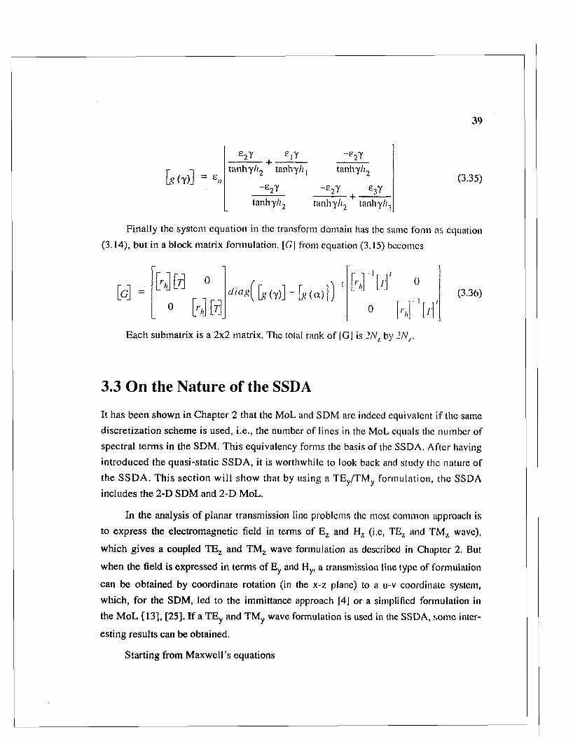
Finally the system equation in the transform domain has the same form as equation
(3.14), but in a block matrix formulation. [G\ from equation (3.15) becomes
[c] =0
[g (y)] " [g (ex)
- i f . /0
(3,36)
Each submatrix is a 2x2 matrix. The total rank of fG| is 2NZ by 2N/:
3.3 On the Nature of the SSDA
It has been shown in Chapter 2 that the MoL and SDM arc indeed equivalent if the same
discretization schem e is used, i.e., the number of lines in the MoL equals the number of
spectral term s in the SDM. This equivalency forms the basis of the SSDA. After having
introduced the quasi-static SSD A, it is worthwhile to look back and study the nature of
the SSD A . This section w ill show that by using a TEy/TM y form ulation, the SSDA
includes the 2-D SDM and 2-D MoL.
In the analysis o f planar transmission line problems the most common approach is
to express the electrom agnetic field in terms of Ez and Hz (i.c, TEZ and TM Z wave),
which gives a coupled TEZ and TM Z wave formulation as described in Chapter 2. But
when the field is expressed in terms o f Ey and Hy, a transmission line type of formulation
can be obtained by coordinate rotation (in the x-z plane) to a u-v coordinate system,
which, for the SDM, led to the immittance approach [4| or a simplified formulation in
the M oL [13], [25]. If a T E y and TM y wave formulation is used in the SSDA, some inter
esting results can be obtained.
Starting from M axwell’s equations

Vx£ = -yoopj)
Vyj) = jm z tl
40
(3.37)
and rearranging the above equation yields a more suitable form for the purpose o f this section
d2 . 2
5 7 + *
d ,2 ?7 + *
Xd2 . d
dxdy J^d=E
. d2 . adydz -/0)fia.v
X. a a 2
_/ Ea= a ja ?
u2_ . a a 2 a ^
(3.38)
//.
A variable transformation in x- and z- direction (this can be either the Fourier trans
form o f the SDM or the orthogonal transform of the MoL) is now introduced as follows
adx
dxd2 2
T z ^ - j a *
d * 2— =- —> -ex .d z 2
(3.39)
Using the lower case to represen t the field com ponents after the transform , equation
(3.38) is written as a decoupled TE/TM to y formulation
0 -a> |i
~j T °a y
where
coe 0
0 - j.d (3.40)

a x and a , can be spectral term s or eigenvalues of the transform matrix, depending on
which m ethod is used in the x- and z-direction, respectively (note: when an eigenvalue is
used, it should be multiplied by j ) . The U matrix corresponds to the coordinate rotation from (x, z, y) to (u, v, y) as shown in Figure 3.5.
Based on the above formulation, the SSDA is really a 2-D SDM when a and a ,
are spectral terms. Similarly, the SSDA becomes a 2-D MoL when a v and a are eigen
values o f the transform matrices (discretization). In the SSDA the SDM and Mol can be
applied separately to the x- and z-direction, respectively, or one can use any one of the
two methods. It is worthwhile to point out that the reason behind the formulation is that
the TEy and TM y modes are independent (not coupled anymore!). On the other hand, this
equivalency is only valid from the formulation point of view. The SSDA has its unique
style in solving discontinuity problem because it uses neither 2-D discretization as in the
MoL nor 2-D basis function as in the SDM.
Figure 3.5 Configuration of general transmission line
In summary

42
• The SSDA combines the M oL and SDM which can be derived from each other
• The SSDA can be formulated from the TEy/TM y wave expansion using a coordinate rotation.
• the 2-D SDM or 2-D M oL are the special case o f a general hybrid method: the SSDA.

45
Chapter 4
The Full-wave SSDA
This chapter focuses on the full-wave SSDA. Two alternative approaches arc presented: an eigenvalue and a deterministic approach.
The foundation of the full-wave SSDA is laid in chapter 2, where only a hom oge
neous boundary condition is used. To calculate the S-parameters of planar circuits, inho-
mogeneous boundary conditions must be included. This chapter describes two different
approaches to implement the inhomogeneous boundary conditions and to extract S-
parameters.
4.1 Eigenvalue Approach
The eigenvalue approach employs the concept of self-consisten t inhomogcncou.s (or
hybrid) boundary conditions at the end o f feed lines which are connected to cither side o f
the discontinuity. This approach makes it possible to simulate the whole structure via an
eigenvalue equation in which the solution is the reflection coefficient of the discontinuity.
The hybrid boundary conditions have been used before in [ 15] and 116], but in the first
case to model the forward and reflected waves individually and in the second case to find
the total field at the launching point by using a modal source approach. In the method p re
sented here, the reflection coefficient (or S (j) is obtained directly,
If a 2-port discontinuity (Figure 4.1) is under investigation, it is assumed that at
some distance from port I of the discontinuity, there will be a standing wave o f the funda
mental mode only consisting of incident and reflected waves:

44
<« <■( -/Pr' yP|*)V = %,{<* - r(1 J
h h( - f t i2 jpAV = v 0 { c + r c J
where |3| is the propagation constant at the boundary o f port 1 calculated separately
by using the SDM, r is the voltage reflection coefficient and are the incident TE/
TM potentials at z = 0, which are solutions o f the homogeneous connecting transmission
line.
Connecting Transmission Line
1
z = 0
DiscontinuityRegion
Connecting Transmission Line
Discretization N,
Figure 4.1 An eigenvalue approach
The inhomogeneous boundary (z-direction) conditions can be derived indepen
dently without considering the spectral dom ain factors (x-direction). With reference to the
matched, open- and short-circuited conditions, at port 2 three different cases for the
boundaries exist, these are the Dirichlet, Neumann and hybrid boundary conditions. For
the matched condition at port 2, there are two choices for the discretization scheme
depending on whether to assign an e or h line as the first line. In the following, the d is
cretization scheme begins with an m (magnctic)-line (open-circuit). When using an m-
line as first line, only the boundary condition for \^'0 is specially treated, while the
boundary condition for is implicitly included. For the same reason, only the bound

45
ary condition for vjc(J is specially treated when using an c-line as the first line.
In case of the matched and opcn-circuit conditions, the hybrid boundary condition at port 1 can be expressed as:
d ' / .„ ( ;lv / (V ' l h-/*<• jxV(> (4 .2)
and at z = 0.5 h
combining equation (4.2) and equation (4.3)
d \ |/Tz
/0.5/ip, 70.5/i|t,•o e - r e h . A
J V\ ./os/ip. 70 5/at.Vi (4.4)-0 .5 h e " +
equation (4.4) can be simplified as
hBydz s (4.5)
z = 0.5//
where
l-y-ctan(0.5/iP1) 1+ /" = ~r~—j'ta.i (0.5/,f5,) T = T 7
The voltage reflection coefficient r is thus explicitly involved in the hybrid bound
ary conditions. At port 2 the matched condition corresponds to:
J ' = -,/T V lV (4-7)
where (32 is the propagation constant at port 2 if a two-port circuit is considered.
The propagation constants and p2 can be derived from the l-D SDM or MOL. Note
that the matched condition corresponds to the discretization scheme o f the opcn-circuit
condition. In a similar way, the hybrid boundary conditions obtained for the short-circuit situation is as follows:

46
3\}/dz
e= - v y , (4.8)
’ = (Nz + 0,5) h
where
x -./tan (0 .5 /jP ,) 1 + / .
1-yxtan (0 .5 /;p [) T 1 - rv = / P i 7 gi,B~~ T = 7— : (4 -9)
Obviously, the potential functions and their first derivatives constitute the character
istic solutions o f the whole circuit. It is interesting to see that the complex functions of
the inhomogeneous boundary conditions at the input described in the above equations are
not only expressed in terms of the propagation constant Pi but also in terms of the dis
cretization interval h and the unknown voltage reflection coefficient r (or ,vn ). In other
words, the inhomogeneous boundary conditions are no longer “static” and strongly
depend on the unknown scattering parameter, which in turn depends on the geometry of
the structure o f interest as well as the operating frequency. This is why the inhomoge
neous boundary conditions are said to be self-consistent.
In sumrr ry, when the load of port 2 is matched, open or short, the corresponding
boundary conditions are listed in the following table (homo=homogeneous boundary con
dition, inhomo=inhomogeneous boundary condition)
port 2 M'*1 vhi H'82 A
matched homo inhomo inhomo homo
open homo inhomo homo homo
short inhom c homo homo homo
Table 4.1. Boundary conditions
It is noted that only the case of inhomogeneous boundary conditic-P need to be spe
cially treated here, because the case of homogeneous boundary condition is discussed in
Chapter 2. Similar to Chapter 2, the determinant equation will be derived from the SSDA
procedure. The solution o f this determinant equation is the unknown reflection coeffi
cient r. The matched condition is taken as an exam ple in the following analysis. The inho- mogcncous boundary conditions are

47
Vdz = "V i
2 = 0 .5 ,'i
chjrdz
(4.10)
'Va-2: = ( A / i + 0 . 5 ) h
in which u and v are the coefficients defined in equation (4.6) and (4.9). in order to
maintain the essential transformation properties (known from the MOL procedure), sym
metric second-order finite-difference operators are required to deal with the Helmholtz
equation and, in particular, the field equations tangential to the interfaces. Using the con
cept and algorithm described in Chapter 2, the electric and magnetic potential vectors in
the original discrete dom ain are normalized by diagonal matrices:
<P = (4.11)
with
J iih 1
r1 f //] =
l/’J 1
Jvh!_
(4.12)
Therefore, the first and second derivatives o f the potential functions arc approxi
mated by formulae sim ilar to the ones in Chapter 2. Note that the unknown voltage reflec
tion coefficient r is directly involved in the first element of [/X',/,J and its related matrices.
Applying the continuity condition at each dielectric interface leads to a matrix rela
tionship between the tangential field components o f two adjacent subregions in the inter
face plane. Next, by successively utilizing the continuity condition and multiplying the
resulting matrices by the transmission line matrices associated with the multilayer subre
gions, the boundary conditions from the top and bottom walls can be transformed into
the interface plane o f the discontinuity. This leads to a kind of space-spcctral Green’s
function in the transform domain which must be transformed back into the original
domain. This step can be performed by the conventional MoL and SDA procedures inde
pendently. From the mathematical viewpoint there is no difference which procedure is
applied first. However, applying the MoL first leads to a better physical understanding
and easier mathematical treatment. As a result, the matrix elements of the resulting

48
G reen’s function in the space-spectral domain are once again coupled to each other through the reverse transformation back into the original domain
\
exb
it A\A- ... \
G alerkin’s technique is again used together with an appropriate choice o f basis
functions which will be defined on the conductor surface for each slicing line in the z-
direction. This leads to a characteristic matrix equation system which m ust be solved for
the zeros of its determinant, whereby the determinant is a function of the reflection coeffi
cient r.
(4.14)
For irregularly shaped discontinuities, the geometric parameters becom e a function
of the z-coordinate and, therefore, are different for each line. In general, this does not
complicate the analysis of planar structures at all, as long as the circuit contour can be
described mathematically or by a set of coordinates. In addition, singularities o f the cir
cuit in the x-direction are automatically considered in the formulation o f the basis func
tions. O nce the voltage reflection coefficient r is known, an arbitrary constant for the first
elem ent o f the x-oriented current coefficients can be assumed. Applying a singular value
decomposition technique yields all the current coefficients for the chosen basis functions
assigned to each discrete line. Therefore, the S-parameters can be extracted from incident
and reflected currents on the strip.
4.2 Deterministic Approach
Although the eigenvalue approach for the full-wave SSDA has the advantages that no 2-
D field distribution calculation is required, the root o f the determinant, w hich is derived
from a large matrix, must be found. For practical applications, a “one-s tep” solution is
most desirable. In this section, a deterministic full-wave SSDA is presented, which avoids
solving an eigenvalue equation by iterative computation.
A deterministic approach was used earlier in the 2-D MoL [12] [26]. In [12] a
“three-step” approach was presented rather than a “one-step” approach because open and

49
short conditions were utilized. In 126] inhomogeneous boundary conditions were intro
duced. B ut based on the au thor’s experience, the resulting algorithm does not provide a
stable solution because a good matching condition for S-parametcr calculation can not be realized.
The key steps in the following approach is to express the field distribution on the
connecting transmission line (far from the discontinuity) as a superposition of incident
and reflected waves, then derive the inhomogeneous boundary conditions for incident
and reflected waves (similar to the previous section, the eigenvalue approach), and
finally combine the incident and reflected waves to satisfy the tangential field condition
at the metallization plane. By solving the 2-D transmission line problem first, the inci
dent w ave distribution is known. The reflected wave distribution is derived by using the
knowledge o f the incident wave.
F igure 4.2 illustrates the deterministic approach. Region B t and C together arc
called region B. Port 2 is always matched.
Connecting Transmission Line
Region A
Region B
Discontinuity Region B j
Connecting Transmission Line
Region C 2
z=0
Nz
Figure 4.2 A deterministic approach
It is assum ed that only one propagation mode exists on the transmission line connected
to port 1, which is so far from the discontinuity region B j, that the higher order modes
excited by the discontinuity have vanished at port I . The same assumption also applies to

50
region C. Using i and r to represent the incident and reflected waves, the inhom ogeneous boundary conditions are expressed as
inc iden t
r e f l e c t e d
< V 'dz
d y
z = 0.5/1
IP i°-5/' h-yPjf vL
-yp, 0 .5/1 h = . i P f Vj
portl (4.15)
z = 0 .5 h
inc iden t
re f l e c t e d 3 i|/dz
z = (Nz + 0.5) //
-yp2o.5/.= -JP2C V,\.\-
-yp20 5/«= -./(V v,Vr
port 2 ( 4 . 1 6 )
: (yvz + o .5 )/i
Similar to equation (4.10), equation (4.15) and equation (4.16) can be simplified as
chydz
fi, r h
= “ Viz = 0 .5 h
Tz
r (4.17)
z = (A 'z + 0 .5 ) h
where
,. -yp,o.5/i ,• yp 0 .5/1 - /p .0 .5/1u = y P j - c u = - j f i f v = - / (32 c ( 4 . 1 8 )
As shown in Chapter 2, two system equations can be obtained for incident and reflected waves respectively
Z (4.19)
Rearranging equation (4.19) and using subscripts A and B to represent fields and currents in different regions, yields

51
i\iJ a 11 • / J a
h_ A H_ vl
h iA11
Jn
Once again G alerkin’s technique is applied (described in chapter 2 and 3) to
expand the unknown incident and reflected currents in terms of known basis functions q
and unknown coefficients C ',r
\ ‘' r./ = 1]
(4.21)
Calculating the inner product of basis functions and using equation (4,20) yields
r -| -i
w'_ 11_ w‘. 12_ C'a = <*■'#' w
w‘L 21
w‘_ 22]
\yr L i i
M/r . 12
K
wr21 wrYy 27 k _ < 4 V
C \4 is the known (from 2-D SDM) coefficient for the current distribution at the connect
ing transmission line at port 1 (region A), CrA is the unknown coefficient of the reflected
current distribution at port 1. Although i and r are used here, both C'n and C n are the
unknown coefficients o f the outgoing current distribution at port 2.
In region A or B, on the metallization, the total tangential electric field must be zero
e + e r = 0 (4.24)
Combining equation (4.22), (4.23) and (4.24) yields
w. * I< 1 + wr
. *Lw 1 . 12
- wr , 12
) c » + wr12
. w‘. 21. 4 + \\h21. W*22- w r22 y „ + wr12
52
where
c‘r = c' + cr (4.26)
C "^ is more useful fo r determ ining the S-param eters. Since C 'A is known, equation
(4.25) can be solved by eliminating C B,
W\
where
IV W<21w",12
IV,. 1V̂22i v ] ! w '
- d t n 2i IV11 C
IV. IV12 iv 12 iv:22 iv:22
(4.27)
(4.28)
In equation (4.27), C A and C'rB are unknown. Because C B is valid in region B t
and C, equation (4.27) can be further simplified by replacing C‘rB by the known coeffi
cients of region C (solution of a homogeneous transmission line) multiplied by an
unknown factor. Thus the number of unknowns is reduced to I in region C no matter
how many lines are used there. Applying the same principle to region A will also reduce
the number of unknowns in region A from NA to I.
Finally, C A and C 'rB can be obtained by simple matrix algebra which is described
in the appendix.
Since the coefficients of the reflected current at port 1 and outgoing current at port
2 are known, the currents can be calculated accordingly. They are defined as I' j and I '2.
Also the incident current obtained from a 2-D SDM analysis is defined as 1+ The S-
parameter can then be calculated by
S.. = (4.29)
^12 =
(4.30)

53
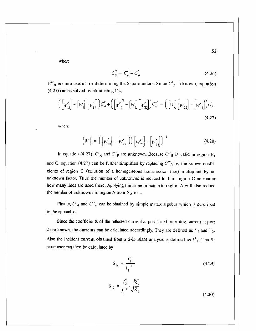
where Z; is the characteristic impedance of the connecting homogeneous transmis
sion line at port / ( /= / , 2).

Chapter 5
Numerical and Experimental Results
5.1 Convergence Analysis of Quasi-static SSDA
A convergence analysis is perform ed for a m icrostrip open-ended d iscon tinu ity , as
shown in Figure 5.1 (er is the dielectric constant and h is the thickness o f the substrate).
Nx is the number o f basis functions in the x-direction. Nz is the number o f lines in the z-
direction. The convergence behavior depends on the number o f spectral term s, Nz, and
Nx. W hen the number of basis functions is increased, the number o f spectral terms must
be increased accordingly. A good convergence behavior is obtained when N z >40, Nx>2,
and the spectral term is greater than 80.
dashdot: tiz=40 Nz=40 N x=l Nx=2
Nz=40Nx=3
solid:Nz=60Nx=2
Nz=60Nx=l
Nz=60Nx=3
LLf
Nz=J0Nx=l
Nz=10 Nz=10Nx=2 Nx=3
dashed Microstrip Open End !
3 0 100# ol spectral terms
Figure 5.1 Convergence analysis of the Quasi-static SSDA (ir //;= /, e r=9.<5)

55
5.2 Simulation Results of Quasi-static SSDA
First o f all the microstrip (MS) and CPW open end, gap and step in width as well as the
CPW air bridge are analyzed by the quasi-static SSDA. Results are shown on Figure 5.2 to Figure 5.8. Those results are used to validate the SSDA.
Figure 5.2 shows the equivalent capacitance o f a microstrip open end. The solid line is calculated by the SSDA. All markers are results from literature.
10
er= l6
10
x x x Full-Wave[33| o o o Quasi-static[22] + + + SDM| 19 J
o
i o '
+- 4 *-'X
* * * SDM[39]
SSDA
ar=9,6
w
10“10 10
w/h1 0 ’
Figure 5.2 Capacitance of microstrip open ends.
Figure 5.3 shows the equivalent capacitances o f a microstrip gap, which is repre
sented by a n network as shown in Figure 3.3. The circles represent the SDM simulation
and stars represent measurements [21]. The solid line is the results of the quasi-static SSDA simulation.

56
GT
45
40
35
30
25
0.20
15
1 0
10
SSDA* * * M easurement [19] o o o SDM [19]
I
20 30 40g a p width (x0.01 mm)
50 60
Figure 5.3 Equivalent capacitance o f a microstrip gap discontinuity. w/h=l h=0 508mmer=8.875
0 9
0 8
V>& 0 7
0 6
0 ,5
0 4
0 3 10
W,
. . 1-
15
S12
W2
20
SSDA
o o o Full-wave[28|
S11
2 5 30 35Frequency (GHz)
, 4. , , . . . . t ..
40 45 50
Figure 5.4 S-parameters o f a microstrip step. w ,= l/nm , \\'2=0,25mm, w/h=l,

57
Figure 5.4 illustrates the S-parameters of a microstrip step discontinuity, which was
derived from network theory, and its shunt capacitance value. The circles represent the
full-wave SDM simulation [30]. The solid line is calculated by the quasi-static SSDA.
Figure 5.5 presents the equivalent capacitance o f an open-ended eoplanar
waveguide compared with published results. The solid line is calculated by the quasi
static SSDA. The circles and stars represent finite difference simulation and m easurement [22], respectively.
Figure 5.6 shows the S-parameters for a eoplanar air-bridge. The circles represent
the results from a full-wave analysis using the Frequency Domain Finite Difference (FDFD) method [31].
Figure 5.7 illustrates the S-parameters of a CPW step discontinuity analyzed in
[32], The solid line is calculated by the SSDA. The circles arc calculated by the full- wave SDM [32].
Figure 5.8 presents the S-parameters of a CPW gap analyzed in |22 |. The solid line
is calculated by the SSDA. The circles represent the results from the quasi-static SDM [22],
In summary, Figure 5.2 to Figure 5.8 present a variety o f planar discontinuities.
The SSDA simulation agrees well with either published results or measurements.

58
30
25
t r20
n3o(tJQ.03% 15 c
10
SSDAo o o Finite Difference [22] * * * Measurement [22]
w
0 2 0 3 0 4 0.5 0,6 0.7 0,8 0.9w/d
Figure 5.5 Equivalent capacitance of a CPW open end. er=y.6, h=0.635, /;/</=/,cJ=\y+2s
0 06
0 ,0 5
0 04
£2-o 03
0 02
0 01
I t
SSDAo o o FDFD [29]
w
° 0 10 20 30 40 s o ' 60 70 8 0 9 0 100F req u en cy (GHz)
Figure 5,6 S-paramctcr of a CPW airbridge. w=l3\im, x= l()\lm , I=3 [On, h~200[Wi,b~3\xni

59
SSDA o o o SDM [30|
S21
S11
2 8 3 0 3 2F req u en cy (GHz)
3 4 3 6 38 40
Figure 5.7 S-parameters of a CPW step. wj-OAimn, u Sj-O .lm m ,w 2=0.4 mm, er~0.S, h=0.254mm
40
35
30
25
c-<d 20 O§
15
O10
5
0
SSDAo o o [221
0 05
Cp2
Cs
W,
sl
i. i Cp1, ,0 1 0 15 0 2 0 25
GapWidth/SubstratoThicKnoss
JSot * w2
0*3
Figure 5.8 Equivalent capacitance o f a CPW gap, (/|»2s j t-H-j, 2+tt’2.‘V'* yh~0,635mm, w^lh-O 2, \ v \ l d l -w ^d l'-O A d , u ' 2 / " 7 "4

60
The main reason why the quasi-static SSDA works extremely well for M H M IC’s is
because the circuit dimensions are small compared with the wavelength, which m eans
the dispersive effect is normally very small (the dispersive effect may become obvious at
very high frequencies). When this condition is not valid (Figure 5.12), visible discrepan
cies to full-wave techniques may occur at lower frequencies.
The computation time of the quasi-static SSDA is typically a few minutes on a
SUN SPARC-2 station (this will give the results over the whole frequency range). It is
noteworthy to point out that results shown from Figure 5.2 to Figure 5.8 do not only dem
onstrate the good agreement with published results, but also show that this method is flex
ible. The accuracy o f this deterministic quasi-static SSDA compares well with full-wave
methods and measurements.
To show the ability of modeling arbitrary discontinuities, microstrip and CPW
MHMIC tapered discontinuities are calculated. The transitions are represented by their
equivalent capacitances as illustrated in Figure 5.9. When the length of the slope, Ws,
increases, the equivalent capacitance decreases. This makes perfect physical sense.
When the length o f the slope equals zero, it represents an abrupt step in width (this was
proved by calculating the capacitance of a step). The whole capacitance curve is quite
smooth which shows the good numerical stability of this method.
The S-param eter of a CPW air bridge is also calculated in terms of air bridge
length, which is shown in Figure 5.10. One can observe that when the air bridge length L
decreases, S j ( decreases too, because the capacitance to the ground decreases.
Figure 5.11 and Figure 5.12 show the limitation of the quasi-static SSDA. Figure
5.11 shows the S-parameters of a microstrip step discontinuity up to 100GHz. Although
at frequencies below 50GHz the comparison with full-wave techniques is excellent,
higher order modes start to propagate on this structure at 60GHz which is not accounted
for in the quasi-static method. This leads to an increase of S n and a decrease in S2i at
about 50GHz.

20wi
substrate.Ws
Q.
Microstrip— w
CPW
Slope Length Ws (m m )
Figure 5.9 Equivalent capacitance of a microstrip and a CPW step/taper. For CPW tv1=0.8mm, s ,=0.1 mm, w2=0.2mm, s2==0.6mm, er=9.6, h=0.254mm. For microstrip,
w 1=1 mm, w2=0.25mm, s r=9.6, h=0.25mm

62
<N
20 40 60 80 100
Frequency (GHz)
Figure 5.10 S-parameters of a CPW airbridge versus bridge length /. \\'=03mm, s-O .lm m , b=3\lm, s r-9 ,6 , h=0.254mm.
1.0 —■-------r " -t ’ i ... -r ..t ... 1 ......
o . y -' - S •
0.8 -
0.7 - 1 Quasi-Staiic SSDA -
0.6 „ ............. Full Wave TLM [33]***
0.5 - , , s , , -•
0.4 -
0.3 - -| ........... w 1=0.25 mm
0.2 - Wi Wi w2=lmm‘■”1 h=0.25
0.1
n n t , , 1 — I---------- 1--------
Er=9.6i
Frequency (GHz)
Figure 5.11 Frequency dependent bcba\ lor of microstrip step

S-P
aram
eter
s
63
1.0-1 f ‘ 1 ■ 1 I < 1 1 ■ I » ‘ I >"l » I < ' !- [ i i I I I I I i I j | - | - | T - | - | I i I I I I I r~pr~rT-r-w-
0 . 8 -
0 . 6 -
- SSDA- MMM 1121 •FDTLMI3.1]
S 1 1 r. —0 . 4 -
0 . 2 -
£r=9.6, h=0.254
0.L0.8 10.2
0 . 0 - I I I I I 1 I I l l l l l l l l l l l l l l . l l l l . i l ■ l - i - i i i 1 i i i i I i i i,, i,_
10 2 0 30
Frequency (GHz)
4 0 5 0
Figure 5.12 Frequency dependent behavior of CPW step

64
5 . 3 C o n v e r g e n c e S t u d y o f F u l l - w a v e S S D A
A co n v erg en ce analysis is perform ed for a microstrip step discontinuity as sh o w n in F ig
ure 5 .1 3 .
1
0 9
........................ t ------- •* -T--................. t ■ - - ~"T.......... . 1 - ■* ----- r .......... -1 - - .......r -----------T -. .... .
*---- -t- - -* - -*■— ;— . ■ * : ..................... r i - ~ -■ ■ -t
0,8 - ■ nz=30
0.7
t2 0 6 w
...... n z= 40 o o o [29) s 21nz=50 + + + [2 9 ]
— nz=601 0 5rS09 0 .4 ------— - --------------- — ----------- ----- _
0 3
0.2
0.1
..,* 1 1 1 S 11
W i ' n W 2
°c- .................— -t-— - - J------- ... x.......................X------- --------- i~ ~ --------- - X ............ i ............. J , - _ -----------x. ... ,
2 4 6 8 10 12 14 16 18 20Freq (GHz)
Figure 5 .13 C onvergency behavior o f the full-w ave SSD Aw 1 — 1 mm, w2=025mm, h=0,25mni, er=l()
W hen the number o f lines (in the propagation direction z) is greater than 50 , con
vergence is achieved.
A s pointed out in Chapter 4, using the approach presented in [26] (u sin g hybrid
boundary conditions) will lead to an unstable solution, because the m atching condition is
applied to on ly one line. U sin g the full-w ave S S D /i, a stable solution can alw ays be
obtained.
5.4 Simulation Results of Full-wave SSDA
A com parison o f S-param eters obtained by the fu ll-w ave S S D A and by others (i.e
|3 0 |) for a microstrip step discontinuity are shown in Figure 5 .I4 and Figure 5 .15. A
good agreem ent can be observed over the frequency range up to 20G H z.

65
1
0 9 SSDA S 12 J0 8 o o o [29] j
0 7 + + + [29] j
co 0 6CDCD
1|
§ 0 5CDQ_^ 0 4
W, . L.... , w2 j}
0 3 iii
0 2 - +L,_„__~ .......
0 1 S u i
4 2 4 6 8 10 12 14 1 r> 18 ,*i) Fieq (GH/)
Figure 5.14 Full-wave S-parameters of a microstrip step W j^ h n m , u’2=0 .5mm, 11=0 .25nun, e,.= I0
i .™~ — ----- r... . . T , .... . . T’ r t r t r r
os " * -*----- ‘r •* A -*» + ♦
0 8 s I2SSDA
0.7 o o o [29]1 1 1 fOOl
t2 0 .6 a»OJw i ■ mk:z n w2.. ;. A A*-. 1
§ 0.5roa.«• 0.4 *r • - i*1* ..... . ... . . . ..
0.3 S i,
0.2
0.1
0 . . --- A • .... A .... XD 2 4 6 i i * . j i i8 10 12 14 16 18 20
Freq (GHz)
Figure 5.15 Full-wave S-paramcters o f a microstrip step w2=0.25mm, h=0.25mm, er =l()

66
Transmission characteristics o f two closely spaced microstrip step discontinuities
arc shown Figure 5.16 (from 2 to 40 GHz). It is evident from the Figure 5.16 (a) that
there is a strong interaction between both steps since their separation is less than half a
guided wavelength. This type o f structure is widely used in filter design. In general, it
behaves like a low-pass filter as in the case of l=1.20mm. The interconnecting stub also
contributes to the dip around 5GHz for the case o f 1=1.20mm. The shorter the length 1, the
further the dip moves towards higher frequencies (as shown in the case o f 1=0.15mm).
Hence the stop band effect occurs only at higher frequencies. Also the Q factor decreases
because the coupling between two homogeneous transmission lines increases. The phase
characteristics o f the S-parameters are shown in Figure 5 .16(b).
0 .6 -,
0.5-
- - I = 1.20 rnm ... I = 0.60 mm— I = 0.30 mm I = 0.15 mm
0.3-
0.2
f (G Hz)
(a)
100-,
50-
X ,
o’
100-1----10 20 40f t o i i / ,•b)
Figure 5.16 S-parameters for a cascaded step discontinuity separated by a transmission line of length 1. W]=0.4mm, \\’o=0.2mm, \v2=0.Smm, er=3.8, h-0 ,25tnm .
(a) Magnitude of S , , , (b) Phase of S , j

67
5.5 Experimental Results
By using a network analyzer at microwave and millimeter wave frequencies, it is
often im possible to directly measure the scattering parameters of a device under test
(DUT). De-embedding techniques must be used to obtain correct S-parameters (36 - 42].
Som e M HM IC discontinuities have been fabricated for experimental investigation.
Figure 5.17 to Figure 5.20 show the calculated (solid line) and measuremcnt(dashed line)
results performed at the University of Victoria. Five MHMIC’s with via holes are tested.
The de-em bedded S-parameters are compared with quasi-static SSDA simulations. All
M HM IC’s are built on 0.254 mm conductor-backed substrate with dielectric constant
9.6. Ground plane via holes are used to suppress the microstrip mode. Figure 5.17 shows
the S-param eters o f a single CPW gap. Figure 5.18 investigates CPW double gaps with
two different resonator lengths. The SSDA calculation shows how the resonant peaks
move when the resonator length changes. Figure 5.18 illustrates the S-paramctcrs of a CPW step discontinuity.

S-pa
ram
eter
s (d
B)
68
[ i i-n-| Ti"i r—j-"i—i-i i | in i | i n i | i i i i | i i i i | i i i-i-q
ExperimentsSSDA
0.0254
Ci-9.6, h=0.254m m
0 1 0 2 0 3 0 4 0Frequency (GHz)
Figure 5.1.7 Measured and computed S-parameters o f a CPW gap
SSDA L=3mm SSDA L=1,5mm Experiment U3mm Experiment L= 1.5mm
0.0508, L |
er=9.6, h=0.254nim
Figure 5.18 Measured and computed S-parameters of end-coupled CPW resonators
S12 (dB)

S11
(dB
)69
SSDAExperiment
er=9.6, h=0.254mm
1 0 0 -<L * i i i l < i i i I i i u I i i i i i ■ ■ ■ ■ i i ..............
Frequency (GHz)
Figure 5.19 Measured and computed S-parameters of a CPW step discontinuity

70
/S
-10
-20
*o- - 3 0 V
SSDA-40
3 □ El □ O l l- - M easurem ent-50
-6026 27 28 29
\\
31 32Freq (GHz)
Figure 5.20 S-param eters of a CPW end-coupled filter. it'=(J.2, s= 0.I5, gap width:25.4\im, resonate, length: 2mm.
Figure 5.20 shows the response of a CPW end-coupled filter. Via holes are also
used to short-circuit the ground-plane and the back-metallization. The SSDA simulation
exactly predicts the position and magnitude of all four resonant peaks which are gener
ated by this 4-pole filter.
In summary, all experimental results agree with our quasi-static SSDA simulation very well.

71
Chapter 6
Conclusion
6.1 Contributions
A fter introducing the generalized form o f the Space-Spectral D om ain Approach
(S S D A ), a new determ inistic quasi-static S S D A has been developed to analyze planar cir
cuit discontinuities.This new approach extends the S S D A to calculate quasi-static capaci
tances and S-parameters o f arbitrarily shaped planar d iscontinuities, T he discontinuity
parameters are derived from an algebraic matrix equation instead o f an e igen va lu e matrix.
T w o new approaches based on the fu ll-w ave Space-Spectral D om ain Approach
(S S D A ) have been proposed to calculate scattering parameters for three-dim ensional d is
continuity problems in M M IC ’s and M H M IC ’s. T he theory presented in this thesis dem
onstrates how to im plem ent self-consistent hybrid boundary cond itions and how to derive
the determ inistic approach.
A com parison o f the results with other m ethods and m easurem ents show s ex ce l
lent agreement up to 40G H z. Results o f som e com plicated structures such as a MHMIO
m icrostrip and CPW taper, C PW air bridge and C PW end-coup led filter arc g iven . Exper
imental validation o f the theoretical results are presented. A lthough the lim ited number
o f exam ples g iven is not representative for all type o f d iscontinuities, this technique by
nature can treat arbitrary planar two-port circuit contours, T his is an advantage o f this
new method which makes it an attractive C A D tool for engineering applications.

72
In sum m ary, the major contributions o f this dissertation arc,
• A generalized S S D A was developed, and a com plete field formulation was given,
• A determ inistic quasi-static SSD A was introduced.
• T he nature o f the S S D A was investigated.
• The se lf con sisten t hybrid boundary conditions have been developed and im plem ented into the full-w ave SSD A .
• A determ inistic full-w ave SSD A w as developed.
• Experim ental work was done to verify the SSD A and to investigate other planar structures.
• A user friendly computer-aided design (C A D ) software package, M H M IC 2.0 , w as developed based on the work o f this thesis.
6.2 Future Work
A lthough exten sive sim ulation and validation were performed in this thesis and a
variety o f discontinuity m odules were included in our CAD software, a uscr-oricnted
softw are can be d evelop ed for more com plicated discontinuities. Another approach is to
use the S S D A algorithm to generate libraries for certain popular CAD packages such as
T O U C H S T O N E ™ or S U P E R CO M PACT™ .
T h e quasi-static S S D A is a very efficient tool to analyze most planar circuits. It can
be extended to opto-electron ic applications, e.g ., for the analysis o f field distribution o f an
electro-optical m odulator as show n in Figure 6.1.
Electrode
Waveguide
Figure 6 . 1 Future application: electro-optic modulator

73
S in ce the SSD A in its present form docs not include the effect o f finite m etallization
thickness and conductor lo sses, tw o different approaches arc proposed to incorporate
finite m etallization:
• u tilize the concept o f surface impedance as it is done in the SDM : add surface im pedance into the G reen’s function to incorporate finite m etallization and conductor loss; the form ulation w ill stay m ostly the sam e as in the
• using the m ode m atching m ethod (M M M ) in conjunction with the MoL: use M M M in the transverse section to incorporate finite m etallization and conductor loss, in the propagation direction (usually called /.-direction) the M oL is used as sam e as in the SSD A .
T he S S D A presumed in this thesis w as applied to a 3-port application in the case o f
the quasi-static SSD A only (Chapter 5). Its formulation w as changed significantly. W ith
out m odifying the formulation, both quasi-static and full w ave SSD A can be used to ana
lyze in -line multi-port discontinuities as show n in Figure 6 .2 , because the discretization in
the z-direction need not to be changed.
To analyze arbitrary multi-port discontinuities as shown in Figure 6,3, the z-diree-
tion-discrctization scheme is not suitable anymore. A possible alternative may be to
choose a small region A and devclope a discretization scheme that takes into account the
SSD A .
z
Figure 6.2 An in-line 3-port discontinuity

special boundary conditions surrounding region A. Then match the field betw een the d is
continuity region and all connected transmission line separately.
Figure 6 .3 Arbitrary multi-port discontinuity

75
Bibliography
ii] A. W exler, “Solution of W aveguide discontinuities by modal analysis,” IEEE Trans, on Microwave Theory Tech., vol. MTT-15, pp. 508-517, Sept. 1967.
[2] E. Yamashita and R. Mittra, “Variational method for the analysis of microstrip line,” IEEE Trans, on M icrowave Theory Tech., vol. A777-16, pp. 251-256, Apr. 1968.
[3] R. M ittra and T. Itoh, “A new technique for the analysis of the dispersion characteristics of microstrip lines”, lEEETruns. on Microwave I'heory Tech,, vol M T T -19 ,N o .l, pp. 47-56, Jan. 1971.
[4] T. Itoh, “Spectral domain immittance approach for dispersion characteristics of generalized printed transmission lines,” IEEE Trans, on Microwave Theory Tech., vol. MTT-2S, pp. 733-736, July 1980.
[5] T. Uw ano and T. Itoh, “Spectral domain approach,” in Numerical Techniques fo r M icrowave and Millimeter Wave Passive Structures, Ch.5, T.ltoh (Ed.), John Wiley, New York, pp. 334-380, 1989.
[6] K.S. Yee, “Numerical solution of initial boundary value problems involving M axw ell’s equation”, IEEE Trans, an Antenna and propagation, Vol. AP-14, pp302-307, May 1966.
[7] O, A. Liskoverts, “The M ethod of Lines,” Review, Differ. Uravneniya, vol. I , pp. 1662-1678, 1965.
[B] U, Schulz and R. Pregla, “A new technique for the analysis of the dispersion characteristics of planar w aveguide,” Arc/i. Elek. i/hertragung, Band 34, pp. 169- 173,1980.
[9] S.B. Worm and R. Pregla, “Hybrid mode analysis of arbitrarily shaped planar m icrowave structure by the m ethod of lines”, IEEE Trans, on Microwave Theory Tech., vol. MTT-28, pp. 191-196, Feb, 1984.
[10] U. Schultz, "C the edge condition with the method of lines in planar waveguides,” A. A Elek. Ueherlragung., vol. 34, pp. 176-178, 1980.
[11] R. Pregla and W. Pascher, “The Method of Lines,” in Numerical Techniques for M icrowave and Millimeter Wave Passive Structures, Ch.5, T.ltoh (Fid.), John Wiley, New York, pp. 381 -446, 1989.

76
, l2J S' o ' “Fuli:Wave ana]ysis of discontinuity in planar waveguides by themethod o f lines using a source approach,” IEEE Trans, on Microwave Theorylech., vol. MTT-38, pp. 1510-1514, Oct. 1990. °
fJ3j R. Pregla and W Pascher, “Diagonalization o f difference operators and system ma nces ,n the Method of Lines,” IEEE Microwave and G uided Wave I I te r sVol. 2, No. 2, pp. 52-54, Feb. 1992. ’
f141 p Te!,i“ * A ‘ Couturier- C - Rumelhard, C. V ernaeyen, P. Cham pion, and D. -ttyo! compact, m onolithic m icrowave dem odulator-m odulator for 6 4 0 A M
“ Si « f ' T n m - " " M ~ r W l ' T e c h " ™
115| H. Diestel anJ S. B. Worm, “Analysis of hybrid field problem s by the method o f lines with non-equidistant discretization,” IEEE Trans, on Microwave Theory lech., vol. MTT-32, pp. 633-638, June 1984. '
fl6J ^ /• R‘ Hoefer- t r a n s m i s s i o n line matrix (TLM ) m ethod”, in Numerical
Und MUlimeU’r WaW Passive ^u e tu re .s , Ch.5, T Itoh (Ed.), John Wiley, New York, pp. 496-591, 1989.
1171 2 R Vahldieck, “A new method of m odeling three-dimensional M IC/. ° ircuits- The sPace-spectral domain approach,” IEEE Trans on Microwave Iheory and Tech., Vol. MTT-32, No.9, pp. 13-09-1318, Sept. 1990.
[18] M. Yu, K. Wu and R. Vahldieck, “A deterministic quasi-static approach to microstrip discontinuity problem in the space-spectral dom ain” IEEE M icrowave and Guided Wave L e t t .y ol. 2, No. 3, pp. 114-116, Mar. 1992.
[19J K. Wu, M Yu and R. Vahldieck, “Rigorous analysis o f 3-D planar circuit discontinuities using the space-spectral domain approach (SSDA) ” ™Im iis. on Microwave Theory and Tech., Vol. MTT-40, No. 7, pp. 1475-1483, July
120] M. Yu R. Vahldieck and K. Wu, “Theoretical and experim ental characterization
I E E E T m m - " " “ " < >
[21] J. Martel, R. R. Boix and M. Hom o, “Static analysis o f microstrip discontinuity using excess charge density in the spectral domain," IEEE Trans on M icrowave Iheory and Tech.. Vol. MTT-39, No.9, pp. 1623-1631, Sept. 1991.
I22J M. Naghcd and I. Wolff, “Equivalent capacitance o f coplanar w avesuide
difference method” T 0* " * ‘ funte
131 “ * R,',Pre?la' “C° Uplin8 ° f Crossed W ™ m ulticonductor269, March 1990. ' "" n m * am lT ” * - M TT-38, no. 3, pp. 265-

[24] P. Silvester and P. Benedek, “Equivalent capacitance of microstrip open end," IEEE Trans, on Microwave Theory and Tech., MTT-20, pp. 511-516, Aug. 1972.
[25] L. Urshev and A. Stoeva, “Application of equivalent transmission line concept to the m ethod o f lines," Microwave and Optical Technology Letters, Vol. 3, No. 10, Oct. 1990.
[26] Z. Chen and B. Gao, “Deterministic approach to full-wave analysis of discontinuities in M lC’s using the method of lines”, IEEE Trans, on Microwave Theory Tech., vol 37, pp.606-611, March 1989.
[27] M . Yu, K. Wu and R. Vahldieck, “Analysis of planar circuit discontinuities using the quasi-static space-spectral domain approach,” Proceedings o f International Symposium o f IEEE Microwave Theory and Tech., Albuquerque, USA, June, pp. 545-848, 1992.
[28] H. Yang, N. G. Alexopoulos and D. R. Jackson, “Microstrip open-end and gap discontinuities in a substrate-superstrate structure,” IEEE Trans on Microwave Theory le c h ., MTT-37, pp. 1542-1546, Oct. 1989.
[29] G. Gronau and I. Wolff, “A simple broad-band device de-embedding method using an autom atic network analyzer with time domain option,” IEEE Trans, on M icrowave Theory and Tech., MTT-37, pp. 479-483, Mar. 1989.
[30] N.H.L. Koster, and R. H. Jansen, “The microstrip step discontinuity: a revised description”, IEEE Trans, on Microwave Theory and Tech., MTT-34, pp. 213- 223, Feb. 1986.
[31] K. Beilenhoff, W. Heinrich, and H.L. Hartnagel, “The scattering behavior of air bridges in coplanar MMIC’S”, Proceedings o f the European Microwave Conference pp. 1131-1135, 1991.
[32] C. Kuo, T. Kitazawa and T. Itoh, “Analysis of shielded coplanar waveguide step discontinuity considering the finite metallization thickness effect”, Proceedings o f 1991 International Symposium o f IEEE Microwave Theory and Tech., vol.2, pp. 473-475, 1991.
[33] H. Jin and R. Vahldieck, “Calculation of frequency-dependent s-paramctcrs of CPW air-bridge considering finite metallization thickness and conductivity” , Proceedings o f 1992 International Symposium o f IEEE Microwave Theory and Tech., Albuquerque, NM, USA, 1992.
[34] Y. R. Sam ii, T. Itoh and R. Mittra, “A spectral domain analysis for solving microstrip discontinuities problems,” IEEE Trans, on Microwave Theory l ech , M TT-22, pp. 372-378, Apr. 1974.
[35] M, Naghed, M. Rittwegcr and I. Wolff, “A new method for calculation of the equivalent inductances of coplanar waveguide discontinuities” , Proceedings o( 1991 International Symposium o f IEEE Microwave Theory and Tech., pp. 747- 750, 1991.

78
|36 | E. F, Da Silva, M. K. McPhun, “Calibration of an automatic network analyzer system using transmission lines o f unknown characteristic impedance, loss and dispersion”, Radio Electron. Eng., Vol. 48, No. 5, pp. 227-234, May 1978.
(371 P.R. Shepherd and R. D. Pollard, “Direct calibration and measurement of microstrip structures on gallium arsenide,” IEEE Trans, on Microwave 'Theory Tech., Vol. MTT-34, pp. 1421-1426, No. 1986.
|38 | G. R. Engen and C. A. Hoer, “Thru-Reflect-Line: An improved technique for calibrating the dual six-port automatic network analyzer,” IEEE Trans, on Microwave Theory Tech., Vol. MTT-27, pp.987-993, Dec. 1979.
[39] R. R. Pantoja, M. J. Howes, J. R. Richardson and R. D. Pollard, “Improved calibration and measurement o f the scattering parameters of microwave integrated circui ts,” IEEE Trans, on Microwave Theory Tech., Vol. MTT-37, pp. 1675-1680, Jan. 1989.
(40] R. Lane, “De-embedding device scattering parameter,” M icrowave J., Vol.27, pp. 149-156, Aug. 1984.
]41] H. J. Eul and Shiek, “Thru-Match-Reflect: An improved technique for calibrating the dual six-port automatic network analyzer,” Technical Report, Ruhr- University Bochum, Institut fu r Hoch and flockstfrecpienztechnik, Bochum, Germany.
[42] M. Yu, “ Microwave Device De-embedding Technique,” Project Report o f ELEC454, Microwave and Optical Communication Systems, Department of Electrical and Computer Engineering, University of Victoria BC, Canada, 1992.
[43] A. Hill and V. K. Tripathi, “An efficient algorithm for the three-dimensional analysis of passive microstrip components and dicontinuities for microwave and millimeter-wave integrated circuits,” IEEE Trans, on M icrowave Theory Tech., Vol. MTT-39, pp. 83-89, Jan. 1991.

71
Appendix
The total number o f lines in the z-dircction:
N = N ,+ N /() Nfl=Nfl,+Nf (F.4)
In region A, one unknown is enough to represent C / because o f the traveling wave
assumption. In region C, the same principle applies. The total number o f unknowns:
C / : I
C/jir: Nfl/-f 1
C / and Cflir can be expressed as
/[}// e '« r
r : - a2' aN, + \'(lN„i + 2' |W'-
1. ('
Combining all left terms of equation (4.27) into one matrix | W ,) yields
M * - K Kwhere
M'',.'i MV'
A = \a,t a2, a i,...,aN +2 j is the unknown coefficient vector.
(K5)
(Kt>)
(K 7)
( m
When N/t>N^/+2, equation (4.27) can be solved.