Embed Size (px)
Citation preview
582 IEEE TRANSACTIONS ON NUCLEAR SCIENCE, VOL. 59, NO. 3, JUNE 2012
A High Load Current, Low-Noise, Area-Efficient,Full On-Chip Regulator for CMOS Pixel Sensors
Jia Wang, Deyuan Gao, Christine Hu-Guo, Kimmo Jaaskelainen, and Yann Hu
Abstract—In order to solve the power distribution problemof detectors in high energy physics experiments, a full on-chipregulator is presented in this paper. It provides the analog powersupply for CMOS pixel sensors. The maximum load current is200 mA. The proposed regulator is stable in the full range ofload current by introducing a zero and adapting the locations ofpoles and zeros. The compensation capacitance and resistanceare significantly decreased to achieve low area. The chip area isonly � ��� ��� excluding the bias and bandgap circuit, whichcan be shared with the other blocks in CMOS pixel sensors. Theexperimental results show that the output noise spectral densityis less than ��� �� �� and �� �� at 1 kHzand 100 kHz, respectively. The power consumption is 1.04 mW atthe voltage of 3.3 V, when the load current is 200 mA.
Index Terms—CMOS pixel sensors, low noise, monolithic activepixel sensors, regulator.
I. INTRODUCTION
I N order to fulfill the new requirements of high energyphysics experiments, some existing vertex detectors are
being upgraded such as the solenoidal tracker at RHIC (STAR).The R&D programs for future vertex detectors are also un-dergoing (e.g., the international linear collider (ILC)). Thenumber of the detection channels is significantly increased inthese plans, where the power distribution becomes an importantissue. In order to improve the power efficiency, the power burnton the thin and long cables must be decreased. Moreover, alarge number of cables introduce large material budget andtake up too much physical space. As the traditional approach,independent powering fails due to its low power efficiency,large power cable budget and large physical space required [1].In order to solve these problems, several alternative schemeshave been reported, such as serial powering, DC-DC con-version and piezoelectric transformers. However, the DC-DC
Manuscript received September 27, 2011; revised January 03, 2012; acceptedFebruary 14, 2012. Date of publication April 13, 2012; date of current versionJune 12, 2012. This work was supported in part by the Chinese ScholarshipCouncil (CSC).
J. Wang is with the School of Computer Science and Technology, North-western Polytechnical University, 710072 Xi’an, China, and also with the In-stitut Pluridisciplinaire Hubert-Curien, University of Strasbourg, CNRS/IN2P3,67037 Strasbourg, France (e-mail: [email protected]).
D. Gao is with the School of Computer Science and Technology, North-western Polytechnical University, 710072 Xi’an, China (e-mail: [email protected]).
C. Hu-Guo, K. Jaaskelainen, and Y. Hu are with the Institut PluridisciplinaireHubert-Curien, University of Strasbourg, CNRS/IN2P3, 67037 Strasbourg,France (e-mail: [email protected]; [email protected];[email protected]).
Color versions of one or more of the figures in this paper are available onlineat http://ieeexplore.ieee.org.
Digital Object Identifier 10.1109/TNS.2012.2188817
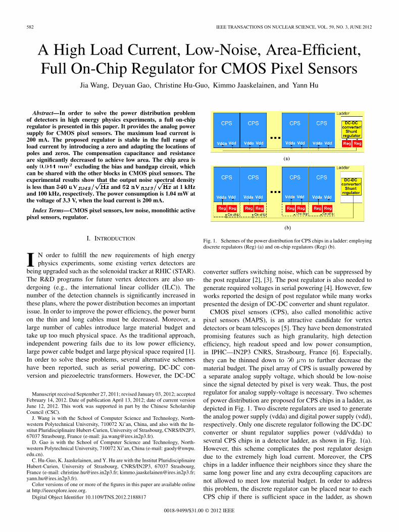
Fig. 1. Schemes of the power distribution for CPS chips in a ladder: employingdiscrete regulators (Reg) (a) and on-chip regulators (Reg) (b).
converter suffers switching noise, which can be suppressed bythe post regulator [2], [3]. The post regulator is also needed togenerate required voltages in serial powering [4]. However, fewworks reported the design of post regulator while many workspresented the design of DC-DC converter and shunt regulator.
CMOS pixel sensors (CPS), also called monolithic activepixel sensors (MAPS), is an attractive candidate for vertexdetectors or beam telescopes [5]. They have been demonstratedpromising features such as high granularity, high detectionefficiency, high readout speed and low power consumption,in IPHC—IN2P3 CNRS, Strasbourg, France [6]. Especially,they can be thinned down to to further decrease thematerial budget. The pixel array of CPS is usually powered bya separate analog supply voltage, which should be low-noisesince the signal detected by pixel is very weak. Thus, the postregulator for analog supply-voltage is necessary. Two schemesof power distribution are proposed for CPS chips in a ladder, asdepicted in Fig. 1. Two discrete regulators are used to generatethe analog power supply (vdda) and digital power supply (vdd),respectively. Only one discrete regulator following the DC-DCconverter or shunt regulator supplies power (vdd/vdda) toseveral CPS chips in a detector ladder, as shown in Fig. 1(a).However, this scheme complicates the post regulator designdue to the extremely high load current. Moreover, the CPSchips in a ladder influence their neighbors since they share thesame long power line and any extra decoupling capacitors arenot allowed to meet low material budget. In order to addressthis problem, the discrete regulator can be placed near to eachCPS chip if there is sufficient space in the ladder, as shown
0018-9499/$31.00 © 2012 IEEE
WANG et al.: A HIGH LOAD CURRENT, LOW-NOISE, AREA-EFFICIENT, FULL ON-CHIP REGULATOR FOR CMOS PIXEL SENSORS 583
in Fig. 1(b). However, the material budget is worsened andthe ladder design becomes complicated. Consequently, it isessential to fully integrate regulators on CPS chip.
In order to generate a low-noise analog supply-voltage andsolve the power distribution problem, a low-noise, area-efficientand full on-chip regulator has been designed. A novel compen-sation strategy has been proposed. The regulator can be stablein the full range of the load current. Low die area and low noiserequirements are also met. A prototype chip was designed andfabricated in a standard 0.35- CMOS process. It is also suit-able for the other low noise applications. This paper is organizedas follows. The power requirements of CPS and design consid-erations are proposed in Section II. Section III introduces thecircuit design. The measurement results are given and discussedin Section IV. Finally, Section V concludes this work.
II. THE POWER REQUIREMENTS OF CPS AND DESIGN
CONSIDERATIONS
In CPS, the analog circuit is composed of a pixel array,column-level discriminators and bias DACs. A zero-suppres-sion logic follows the column-level discriminator to compressthe transmitted data. Two memory blocks store the data and areoperated in a Ping-Pong mode. The analog circuit and digitalcircuit are powered by vdda and vdd, respectively. In order tomeet the air-cooling requirement in ILC, power pulsing is pro-posed to be used [7], [8]. During the collision (1 ms), CPS areoperated in full speed. A current of about 200 mA will be con-sumed by the analog core circuit. On the other hand, all or someblocks will be standby/shutdown in the off interval (199 ms).Very low current near zero will be consumed. Moreover, thesituation of low load current also happens in CPS during theirstart-up, in which three states are included. In the ”power-onreset” state, the regulators and bandgaps start to work. Thenthe buffers and the digital to analog converters (DACs) start tosupply reference voltages and bias voltages for the other blocks.Finally, the pixels are readout in rolling-shutter readout modeand the column-level discriminators digitize the output comingfrom the pixels. Therefore, the load current dramatically variesduring the start-up. Its range is approximately from 0 mA to200 mA. The regulator of analog power supply may work inzero-load, light-load or heavy-load cases. Thus, the regulator tobe designed must be stable in the full range of the load current.
The parasitic capacitance in CPS should not be neglected dueto the long and wide power wires. It becomes significantly largein a large pixel array. Moreover, it is very difficult to directly ex-tract the total parasitic capacitance from the layout of the wholesensor chip (about ). The minimum value is estimated as200 nF in this design according to the parasite extraction fromthe layout of each analog block. It is noted that the parasitic ca-pacitances beyond these blocks are not taken into account andthe parasitic capacitance varies with process fluctuation. There-fore, design margin must be considered. With such a large ca-pacitance and a large load current range, the output pole locationsignificantly varies with the load current [9] and it must be thedominant pole at low-load condition. In addition, any externalcomponent is not allowed to achieve a full on-chip regulator. Inorder to guarantee the stability in the full range of load current,a novel compensation strategy is proposed. The regulator em-
ploys a series RC network, which introduces a zero to compen-sate the phase. Moreover, the locations of the poles and zeros areadapted by the current feedback. They move towards the samedirection as the output pole does. Thus, the output pole is alwaysthe dominant pole at the light load or heavy load. The next sec-tion will present the stability analysis in detail.
The power supply rejection (PSR) performance is importantin this design. Especially, the regulator is used following theDC-DC converter in the power system of detectors. Since theinductor must be air-core, the DC-DC converter usually worksat the frequency of higher than 1 MHz to supply high current[2]. In order to suppress the switching noise, the PSR should behigh at high frequency. The noise induced by the regulator isalso needed to be low. Moreover, low power is required due tothe cooling system and the silicon area is severely limited to befully built in CPS.
III. CIRCUIT DESIGN
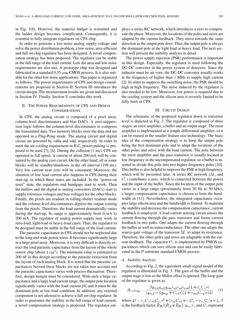
The schematic of the proposed regulator down to transistorlevel is depicted in Fig. 2. The regulator is composed of threestages: an error amplifier, a buffer and an output stage. The erroramplifier is implemented as a simple differential amplifier, so itcan be reused in the smaller feature size technology. The basicidea of the compensation strategy is to keep the output polebeing the first dominant pole and to adapt the locations of theother poles and zeros with the load current. The pole betweenthe error amplifier and the pass transistor is usually located atlow frequency in the uncompensated regulator, so a buffer is in-serted to divide this pole into two higher-frequency poles [10].This buffer is also helpful to improve the PSR at high frequency,which will be presented later. A series RC network ( and
) contributes a zero, which is connected between the powerand the input of the buffer. Since the location of the output polevaries in a large range (proximately from 30 Hz to 50 kHz),a larger compensation capacitance is chosen to limit the band-width in [11]. Nevertheless, the integrated capacitance occu-pies large silicon area and the bandwidth is limited. To maintainthe stability and decrease the compensation capacitance, currentfeedback is employed. A load current sensing circuit senses thecurrent flowing through the pass transistor and forms currentfeedback in two paths. One adapts the current flowing throughthe buffer as well its transconductance. The other one adapts thesource-gate voltage of the transistor to adapt its resistance.Therefore, the other poles and zeros are adaptable with the cur-rent feedback. The capacitor is implemented by PMOS ca-pacitances which can save silicon area and can be easily fabri-cated in the P-substrate standard CMOS process.
A. Stability Analysis
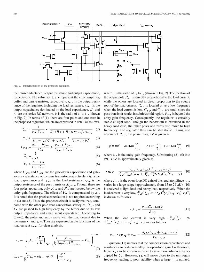
According to Fig. 2, the equivalent small-signal model of theregulator is illustrated in Fig. 3. The gain of the buffer and theoutput stage is low so the Miller-effect is ignored. The loop-gainof the regulator is given as
(1)
where ,is the feedback factor . , and represent
584 IEEE TRANSACTIONS ON NUCLEAR SCIENCE, VOL. 59, NO. 3, JUNE 2012
Fig. 2. Implementation of the proposed regulator.
the transconductance, output resistance and output capacitance,respectively. The subscript represent the error amplifier,buffer and pass transistor, respectively. is the output resis-tance of the regulator including the load resistance. is theoutput capacitance dominated by the load capacitance. and
are the series RC network. is the radio of to , (shownin Fig. 2). In terms of (1), there are four poles and one zero inthe proposed regulator, which are expressed in detail as follows.
(2)
(3)
(4)
(5)
(6)
where and are the gate-drain capacitance and gate-source capacitance of the pass transistor, respectively. is theload capacitance and is the load resistance. is theoutput resistance of the pass transistor . Though there arefour poles appearing, only and are located below theunity-gain frequency. The effect of is compensated by .It is noted that the precise cancelation is not required accordingto (3) and (5). Thus, the proposed circuit is easily realized, com-pared with the other pole-zero cancelation strategies. and
are pushed to high frequency by the buffer due to its lowoutput impedance and small input capacitance. According to(3)–(6), the poles and zeros move with the load current due tothe terms and . They are expressed as the functions of theload current for clear analysis.
(7)
(8)
where is the radio of to (shown in Fig. 2). The location ofthe output pole is directly proportional to the load current,while the others are located in direct proportion to the squareroot of the load current. is located at very low frequencywhen the load current is low. and are small since thepass transistor works in subthreshold region. is beyond theunity-gain frequency. Consequently, the regulator is certainlystable at light load. Though the bandwidth is extended in theheavy load case, the other poles and zeros also move to highfrequency. The regulator thus can be still stable. Taking intoaccount of , the phase margin is given as
(9)
where is the unity-gain frequency. Substituting (3)–(5) into(9), is approximately given as,
(10)
where is the open-loop DC gain of the regulator. Sincevaries in a large range (approximately from 15 to ), (10)is analyzed at light load and heavy load, respectively. When theload current is very low,is drawn as follows
(11)
When the load current is very high,is drawn as follows
(12)
Equation (11) implies that the compensation capacitance andresistance can be decreased by the open-loop gain. Furthermore,larger can be chosen in order to save more silicon area oc-cupied by . However, will move close to the unity-gainfrequency leading to poor stability when a large is utilized.
WANG et al.: A HIGH LOAD CURRENT, LOW-NOISE, AREA-EFFICIENT, FULL ON-CHIP REGULATOR FOR CMOS PIXEL SENSORS 585
Fig. 3. Equivalent small-signal model of the proposed regulator.
Fig. 4. Optimization of� and� .
Assuming that the other parameters are given, the tradeoff be-tween silicon area and stability is shown in Fig. 4. Since and
are realized by transistor and (shown in Fig. 2), re-spectively, their values are presented by width and length. Thephase margin is certainly improved with larger . However, theimprovement is around 10 with five time increase in the dimen-sion of . In terms of the silicon area limitation, the dimensionof is chosen as , which generates acapacitance of about 10.5 pF. is chosen as .
The stability of the proposed regulator is verified bySPECTER when the load capacitance is 200 nF. Fig. 5 showsthe frequency response of the regulator as the load currentvaries. It demonstrates that the poles and zeros move to higherfrequency when the load current becomes larger. The phasemargin of regulator is larger than 45 over the full range ofload current. Moreover, the minimum phase margin happens atthe load current of 7 mA. In this case, the pass transistor enterssaturated region from subthreshold region so its gate-sourcecapacitance and gate-drain capacitance dramatically increase,according to the volt-capacitance of CMOS capacitor. On theother hand, the feedback current is low so is close tothe unity-gain frequency. The phase margin begins to increasewhen the load current continues to increase. The simulationresults also verify (12). and should be large enough toguarantee the stability at the load current of 7 mA.
B. Dropout Voltage and PSR
The dropout voltage is required to be low to achieve highpower efficiency. It is only 0.3 V in this design. Thus, the passtransistor is undoubtedly very large if it works in the saturatedregion. In addition, quiescent current also increases. The chiparea and power dissipation become large. Therefore, the passtransistor is designed to work in linear region at heavy load and
Fig. 5. Open-loop frequency responses at load current of 0 mA, 7 mA and 200mA when load capacitance is 200 nF.
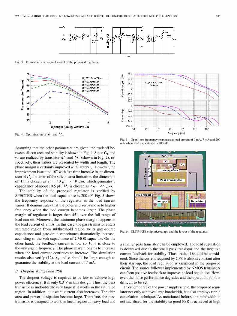
Fig. 6. ULTIMATE chip micrograph and the layout of the regulator.
a smaller pass transistor can be employed. The load regulationis decreased due to the small pass transistor and the negativecurrent feedback for stability. Thus, tradeoff should be consid-ered. Since the current required by CPS is almost constant aftertheir start-up, the load regulation is sacrificed in the proposedcircuit. The source follower implemented by NMOS transistorscan form positive feedback to improve the load regulation. How-ever, the noise performance degrades and the operation point isdifficult to be set.
In order to free of the power supply ripple, the proposed regu-lator not only achieves large bandwidth, but also employs ripplecancelation technique. As mentioned before, the bandwidth isnot sacrificed for the stability so good PSR is achieved at high
586 IEEE TRANSACTIONS ON NUCLEAR SCIENCE, VOL. 59, NO. 3, JUNE 2012
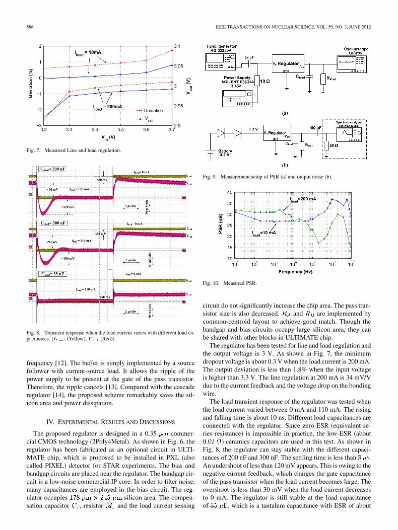
Fig. 7. Measured Line and load regulation.
Fig. 8. Transient response when the load current varies with different load ca-pacitances. (� (Yellow), � (Red)).
frequency [12]. The buffer is simply implemented by a sourcefollower with current-source load. It allows the ripple of thepower supply to be present at the gate of the pass transistor.Therefore, the ripple cancels [13]. Compared with the cascaderegulator [14], the proposed scheme remarkably saves the sil-icon area and power dissipation.
IV. EXPERIMENTAL RESULTS AND DISCUSSIONS
The proposed regulator is designed in a 0.35- commer-cial CMOS technology (2Poly4Metal). As shown in Fig. 6, theregulator has been fabricated as an optional circuit in ULTI-MATE chip, which is proposed to be installed in PXL (alsocalled PIXEL) detector for STAR experiments. The bias andbandgap circuits are placed near the regulator. The bandgap cir-cuit is a low-noise commercial IP core. In order to filter noise,many capacitances are employed in the bias circuit. The reg-ulator occupies silicon area. The compen-sation capacitor , resistor and the load current sensing
Fig. 9. Measurement setup of PSR (a) and output noise (b).
Fig. 10. Measured PSR.
circuit do not significantly increase the chip area. The pass tran-sistor size is also decreased. and are implemented bycommon-centroid layout to achieve good match. Though thebandgap and bias circuits occupy large silicon area, they canbe shared with other blocks in ULTIMATE chip.
The regulator has been tested for line and load regulation andthe output voltage is 3 V. As shown in Fig. 7, the minimumdropout voltage is about 0.3 V when the load current is 200 mA.The output deviation is less than 1.8% when the input voltageis higher than 3.3 V. The line regulation at 200 mA is 34 mV/Vdue to the current feedback and the voltage drop on the bondingwire.
The load transient response of the regulator was tested whenthe load current varied between 0 mA and 110 mA. The risingand falling time is about 10 ns. Different load capacitances areconnected with the regulator. Since zero-ESR (equivalent se-ries resistance) is impossible in practice, the low-ESR (about
) ceramics capacitors are used in this test. As shown inFig. 8, the regulator can stay stable with the different capaci-tances of 200 nF and 300 nF. The settling time is less than .An undershoot of less than 120 mV appears. This is owing to thenegative current feedback, which charges the gate capacitanceof the pass transistor when the load current becomes large. Theovershoot is less than 30 mV when the load current decreasesto 0 mA. The regulator is still stable at the load capacitanceof , which is a tantalum capacitance with ESR of about
WANG et al.: A HIGH LOAD CURRENT, LOW-NOISE, AREA-EFFICIENT, FULL ON-CHIP REGULATOR FOR CMOS PIXEL SENSORS 587
TABLE ITHE PERFORMANCE COMPARISONS OF THE PROPOSED WORK AND REPORTED WORK
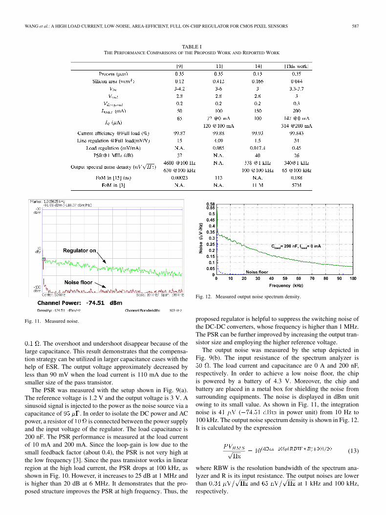
Fig. 11. Measured noise.
. The overshoot and undershoot disappear because of thelarge capacitance. This result demonstrates that the compensa-tion strategy can be utilized in larger capacitance cases with thehelp of ESR. The output voltage approximately decreased byless than 90 mV when the load current is 110 mA due to thesmaller size of the pass transistor.
The PSR was measured with the setup shown in Fig. 9(a).The reference voltage is 1.2 V and the output voltage is 3 V. Asinusoid signal is injected to the power as the noise source via acapacitance of . In order to isolate the DC power and ACpower, a resistor of is connected between the power supplyand the input voltage of the regulator. The load capacitance is200 nF. The PSR performance is measured at the load currentof 10 mA and 200 mA. Since the loop-gain is low due to thesmall feedback factor (about 0.4), the PSR is not very high atthe low frequency [3]. Since the pass transistor works in linearregion at the high load current, the PSR drops at 100 kHz, asshown in Fig. 10. However, it increases to 25 dB at 1 MHz andis higher than 20 dB at 6 MHz. It demonstrates that the pro-posed structure improves the PSR at high frequency. Thus, the
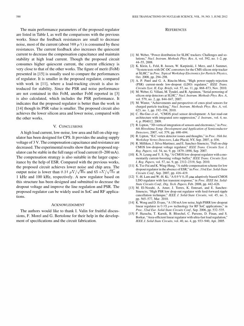
Fig. 12. Measured output noise spectrum density.
proposed regulator is helpful to suppress the switching noise ofthe DC-DC converters, whose frequency is higher than 1 MHz.The PSR can be further improved by increasing the output tran-sistor size and employing the higher reference voltage.
The output noise was measured by the setup depicted inFig. 9(b). The input resistance of the spectrum analyzer is
. The load current and capacitance are 0 A and 200 nF,respectively. In order to achieve a low noise floor, the chipis powered by a battery of 4.3 V. Moreover, the chip andbattery are placed in a metal box for shielding the noise fromsurrounding equipments. The noise is displayed in dBm unitowing to its small value. As shown in Fig. 11, the integrationnoise is ( in power unit) from 10 Hz to100 kHz. The output noise spectrum density is shown in Fig. 12.It is calculated by the expression
(13)
where RBW is the resolution bandwidth of the spectrum ana-lyzer and R is its input resistance. The output noises are lowerthan and at 1 kHz and 100 kHz,respectively.
588 IEEE TRANSACTIONS ON NUCLEAR SCIENCE, VOL. 59, NO. 3, JUNE 2012
The main performance parameters of the proposed regulatorare listed in Table I, as well the comparisons with the previousworks. Since the feedback resistances are small to decreasenoise, most of the current (about ) is consumed by theseresistances. The current feedback also increases the quiescentcurrent to decrease the compensation capacitance and maintainstability at high load current. Though the proposed circuitconsumes higher quiescent current, the current efficiency isvery close to that of the other works. The figure of merit (FoM)presented in [15] is usually used to compare the performancesof regulator. It is smaller in the proposed regulator, comparedwith work in [11], where a load-tracking circuit is also in-troduced for stability. Since the PSR and noise performanceare not contained in this FoM, another FoM reported in [3]is also calculated, which includes the PSR performance. Itindicates that the proposed regulator is better than the work in[14] though its PSR value is smaller. The proposed circuit alsoachieves the lower silicon area and lower noise, compared withthe other works.
V. CONCLUSIONS
A high load current, low-noise, low area and full on-chip reg-ulator has been designed for CPS. It provides the analog supplyvoltage of 3 V. The compensation capacitance and resistance aredecreased. The experimental results show that the proposed reg-ulator can be stable in the full range of load current (0–200 mA).The compensation strategy is also suitable in the larger capac-itance by the help of ESR. Compared with the previous works,the proposed circuit achieves lower noise and chip area. Theoutput noise is lower than and at1 kHz and 100 kHz, respectively. A new regulator based onthis structure has been designed and submitted to decrease thedropout voltage and improve the line regulation and PSR. Theproposed regulator can be widely used in SoC and RF applica-tions.
ACKNOWLEDGMENT
The authors would like to thank I. Valin for fruitful discus-sions, F. Morel and G. Bertolone for their help in the develop-ment of specifications and the circuit fabrication.
REFERENCES
[1] M. Weber, “Power distribution for SLHC trackers: Challenges and so-lutions,” Nucl. Instrum. Methods Phys. Res. A, vol. 592, no. 1–2, pp.44–55, 2008.
[2] K. Klein, L. Feld, R. Jussen, W. Karpinski, J. Merz, and J. Sammet,“System tests with DC-DC converters for the CMS silicon strip trackerat SLHC,” in Proc. Topical Workshop Electronics for Particle Physics,Oct. 2008, pp. 294–298.
[3] A. P. Patel and G. A. Rincón-Mora, “High power-supply-rejection(PSR) current-mode low-dropout (LDO) regulator,” IEEE Trans.Circuits Syst. II, Exp. Briefs, vol. 57, no. 11, pp. 868–873, Nov. 2010.
[4] M. Weber, G. Villani, M. Tyndel, and R. Apsimon, “Serial powering ofsilicon strip detectors at SLHC,” Nucl. Instrum. Methods Phys. Res. A,vol. 579, no. 2, pp. 844–847, 2007.
[5] M. Winter, “Achievements and perspectives of cmos pixel sensors forcharged particle tracking,” Nucl. Instrum. Methods Phys. Res. A, vol.623, no. 1, pp. 192–194, 2010.
[6] C. Hu-Guo et al., “CMOS pixel sensor development: A fast read-outarchitecture with integrated zero suppression,” J. Instrum., vol. 4, no.4, p. P04012, 2009.
[7] R. Lipton, “3D-vertical integration of sensors and electronics,” in Proc.6th Hiroshima Symp. Development and Application of SemiconductorDetectors, 2007, vol. 579, pp. 690–694.
[8] R. Lipton, “ILC vertex detector issues and thoughts,” in Proc. 16th Int.Workshop Vertex Detectors, Lake Placid, NY, Sep. 2007, p. 036.
[9] R. Milliken, J. Silva-Martinez, and E. Sanchez-Sinencio, “Full on-chipCMOS low-dropout voltage regulator,” IEEE Trans. Circuits Syst. I,Reg. Papers, vol. 54, no. 9, pp. 1879–1890, Sep. 2007.
[10] K. N. Leung and Y. S. Ng, “A CMOS low-dropout regulator with a mo-mentarily current-boosting voltage buffer,” IEEE Trans. Circuits Syst.I, Reg. Papers, vol. 57, no. 9, pp. 2312–2319, Sep. 2010.
[11] K. Tsz-Fai and K. Wing-Hung, “A stable compensation scheme for lowdropout regulator in the absence of ESR,” in Proc. 33rd Eur. Solid-StateCircuits Conf., Sep. 2007, pp. 416–419.
[12] Y.-H. Lam and W.-H. Ki, “A 0.9 V ���� �� adaptively biased CMOSLDO regulator with fast transient response,” in Proc. IEEE Int. Solid-State Circuits Conf., Dig. Tech. Papers, Feb. 2008, pp. 442–626.
[13] M. El-Nozahi, A. Amer, J. Torres, K. Entesari, and E. Sanchez-Sinencio, “High PSR low drop-out regulator with feed-forward ripplecancellation technique,” IEEE J. Solid-State Circuits, vol. 45, no. 3,pp. 565–577, Mar. 2010.
[14] K. Wong and D. Evans, “A 150 mA low noise, high PSRR low-dropoutlinear regulator in ���� �� technology for RF SoC applications,” inProc. 32nd Eur. Solid-State Circuits Conf., Sep. 2006, pp. 532–535.
[15] P. Hazucha, T. Karnik, B. Bloechel, C. Parsons, D. Finan, and S.Borkar, “Area-efficient linear regulator with ultra-fast load regulation,”IEEE J. Solid-State Circuits, vol. 40, no. 4, pp. 933–940, Apr. 2005.