Embed Size (px)
Citation preview
A. Growth mechanism of CHQ nanospheres and nanolenses
A1. Schematic of the growing mechanism Figure S1 Schematic representation for self-assembling of CHQ nanostructures. a, Model structure of a monomer. b, Model structure of the strong hydrogen bond array composing the frameworks of CHQ nanotubes. The red and white balls denote the oxygen and hydrogen atoms of hydroxyl (-OH) groups forming the intermolecular hydrogen bonds. c, Model for temperature-induced breaking of the hydrogen bond array. d, Model structures of re-assembled small CHQ clusters. ‘n’ denotes the number of CHQ molecules. e. Scheme of growing lenses, hemispheres and spheres. f, SEM image of the hemispheres growing on the crystal surface.
Various self-assembled CHQ nanostructures1 can be obtained by changing temperature
and/or evaporation rate. The change of temperature can be a substantial factor to re-
assemble a given CHQ nanostructure into another morphology. For instance, when CHQ
nanotubes grown at -14℃ are heated at 40℃ in aqueous environments, the CHQ crystals
become unstable. The CHQ molecules released from the destabilized crystals re-assemble
into nanospheres consisting of dimer/hexamer-based units of CHQ. Besides raising
SUPPLEMENTARY INFORMATIONdoi: 10.1038/nature08173
www.nature.com/nature 1
temperature, CHQ nanospheres may be assembled by allowing evaporation to occur for a
week. Once the nanospheres are formed, they are stable both in aqueous and dry
conditions and are resistant to temperature change up to ~ 150 ºC.
Figure S2 IR analyses of CHQ nanostructures.
In the IR spectra of CHQ nanospheres, the strong –OH stretching peak at ~3190
cm-1 originating from one-dimensional strongly hydrogen-bonded chains almost
disappears (Fig. S2). This implies that the tubular frameworks of hydrogen bonds
gradually disappear during conversion from nanotubes to nanospheres. Though the –CH2
stretching peak around ~2900 cm-1 for nanotubes and monomers is very small, that for
nanospheres is strong because the –CH2 moieties of the dimer/hexamer are involved in π-
H bonding with adjacent dimers/hexamers, which is consistent with the IR spectra of the
CHQ nanospheres. In addition, the shift of hydrogen-bonded –OH bending peaks from
~1699 cm-1 to ~1653 cm-1 corresponds to the ab initio calculation2 that hydrogen bonds
of the dimer/hexamer-based assemblies are weaker than the one-dimensional hydrogen
bonds of the nanotubes by ~3kcal/mol.
doi: 10.1038/nature08173 SUPPLEMENTARY INFORMATION
www.nature.com/nature 2
A2. Thermodynamical Analysis
a b
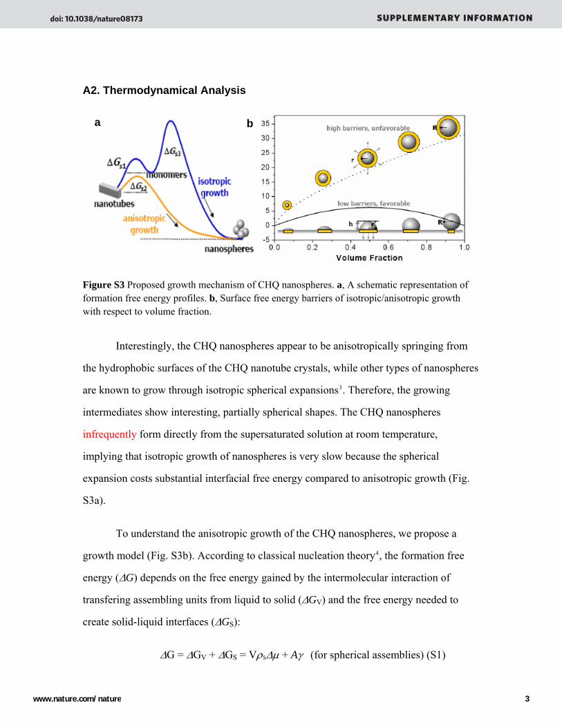
Figure S3 Proposed growth mechanism of CHQ nanospheres. a, A schematic representation of formation free energy profiles. b, Surface free energy barriers of isotropic/anisotropic growth with respect to volume fraction.
Interestingly, the CHQ nanospheres appear to be anisotropically springing from
the hydrophobic surfaces of the CHQ nanotube crystals, while other types of nanospheres
are known to grow through isotropic spherical expansions3. Therefore, the growing
intermediates show interesting, partially spherical shapes. The CHQ nanospheres
infrequently form directly from the supersaturated solution at room temperature,
implying that isotropic growth of nanospheres is very slow because the spherical
expansion costs substantial interfacial free energy compared to anisotropic growth (Fig.
S3a).
To understand the anisotropic growth of the CHQ nanospheres, we propose a
growth model (Fig. S3b). According to classical nucleation theory4, the formation free
energy (ΔG) depends on the free energy gained by the intermolecular interaction of
transfering assembling units from liquid to solid (ΔGV) and the free energy needed to
create solid-liquid interfaces (ΔGS):
ΔG = ΔGV + ΔGS = VρSΔμ + Aγ (for spherical assemblies) (S1)
doi: 10.1038/nature08173 SUPPLEMENTARY INFORMATION
www.nature.com/nature 3
where V is the volume of nanospheres, Δμ (<0) is the difference in chemical potential of
the solid and the liquid, A is the surface area for growth and γ is the interfacial free
energy density. In the case of equal volumes, spherical shapes with minimum surface
area are always thermodynamically most stable. However, their growth rate depends
more on the actual surface area of growth where incoming molecules form an additional
layer on the surface, which can be described as:
Ai = 4π r2 (for isotropic growth of a sphere) (S2)
Aa = π r'2 (for anisotropic growth of a sphere) (S3)
where r is the radius of the intermediate spheres and r´ is the radius of the area in contact
with the crystal surface (Fig. S3b). The interfacial free energies for isotropic growth and
anisotropic growth can be represented as a function of volume fraction under the
assumption that γ is not significantly different for anisotropic and isotropic growth. The
graph shows that the interfacial free energy of isotropic growth is larger than that of
anisotropic growth. Therefore, anisotropic growth is always kinetically favorable, though
the isotropic intermediates are always thermodynamically more stable. The schematic
representation in Fig. S3a summarizes the formation process of CHQ nanospheres. The
direct formation of CHQ nanospheres from solvated monomers is unfavorable because of
the high interfacial free energy barriers for isotropic growth. Instead, the monomers
crystallize into CHQ nanotube crystals first and then follow the low-energy barrier path
of anisotropic growth to form CHQ nanospheres.
doi: 10.1038/nature08173 SUPPLEMENTARY INFORMATION
www.nature.com/nature 4
Figure S4 a, Schematic representation of the surface free energy barrier of growing CHQ nanolenses. b, A SEM image of CHQ lenses attached to CHQ nanotube crystals. c, A SEM image showing the morphology conversion from CHQ nanolenses to spheres.
The film-like structures of CHQ often cover the surface of CHQ crystals. In this
case, the CHQ molecules released from the surface of crystals cannot diffuse into
solution directly. Instead, they are concentrated within a small volume under the film,
which induces high chemical potentials (Δμ) leading to fast nucleation and kinetic growth
of disk-shaped structures (Fig. S4a, left). At lower temperatures around –10°C, the disks
seem to grow kinetically even without the assistance of film structures. Then, the
spherical curvatures are formed as the released CHQ molecules take part in the self-
assembly (Fig. S4a, right). The growing surface areas for disks and lenses can be
represented respectively as:
Ai' = 2πR·t (for 2D isotropic growth of a disk) (S4)
Aa' = π R'2 (for anisotropic growth of a lens) (S5)
doi: 10.1038/nature08173 SUPPLEMENTARY INFORMATION
www.nature.com/nature 5
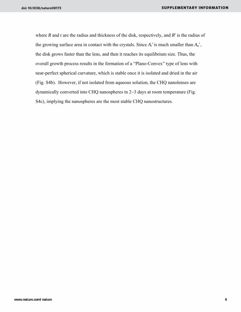
where R and t are the radius and thickness of the disk, respectively, and R' is the radius of
the growing surface area in contact with the crystals. Since Ai' is much smaller than Aa' ,
the disk grows faster than the lens, and then it reaches its equilibrium size. Thus, the
overall growth process results in the formation of a “Plano-Convex” type of lens with
near-perfect spherical curvature, which is stable once it is isolated and dried in the air
(Fig. S4b). However, if not isolated from aqueous solution, the CHQ nanolenses are
dynamically converted into CHQ nanospheres in 2~3 days at room temperature (Fig.
S4c), implying the nanospheres are the most stable CHQ nanostructures.
doi: 10.1038/nature08173 SUPPLEMENTARY INFORMATION
www.nature.com/nature 6
B. Near-Field Optics of a Nanolens
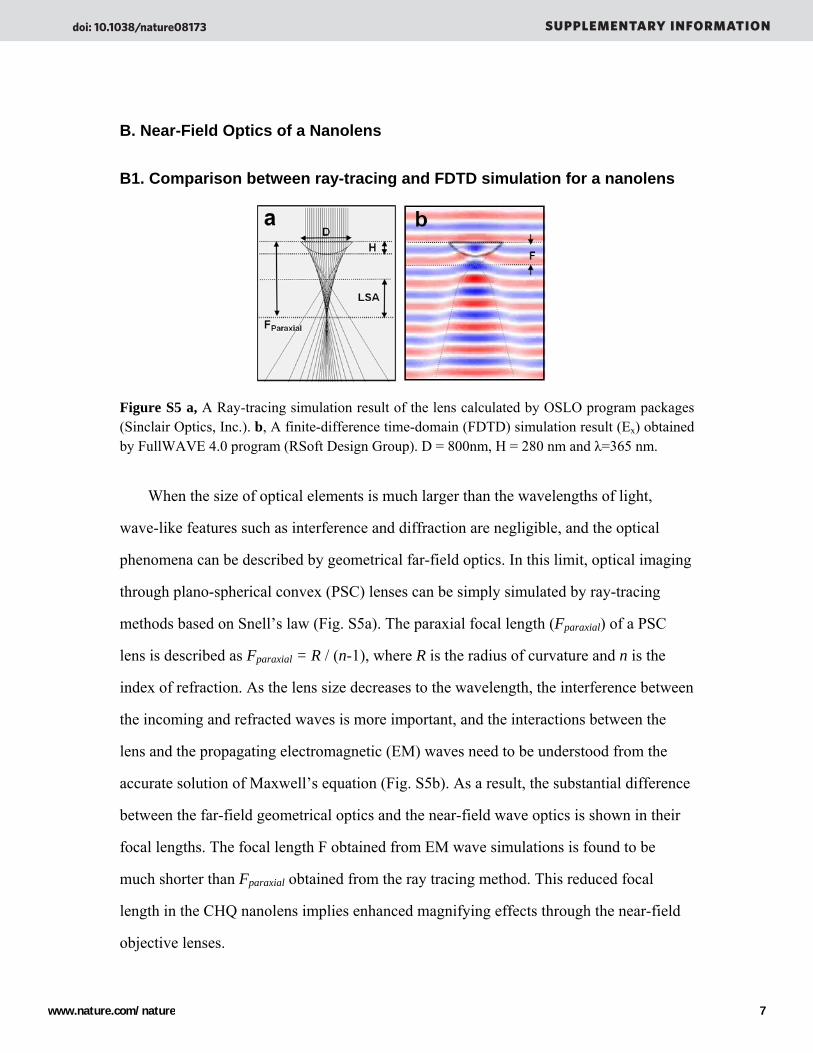
B1. Comparison between ray-tracing and FDTD simulation for a nanolens
Figure S5 a, A Ray-tracing simulation result of the lens calculated by OSLO program packages (Sinclair Optics, Inc.). b, A finite-difference time-domain (FDTD) simulation result (Ex) obtained by FullWAVE 4.0 program (RSoft Design Group). D = 800nm, H = 280 nm and λ=365 nm.
When the size of optical elements is much larger than the wavelengths of light,
wave-like features such as interference and diffraction are negligible, and the optical
phenomena can be described by geometrical far-field optics. In this limit, optical imaging
through plano-spherical convex (PSC) lenses can be simply simulated by ray-tracing
methods based on Snell’s law (Fig. S5a). The paraxial focal length (Fparaxial) of a PSC
lens is described as Fparaxial = R / (n-1), where R is the radius of curvature and n is the
index of refraction. As the lens size decreases to the wavelength, the interference between
the incoming and refracted waves is more important, and the interactions between the
lens and the propagating electromagnetic (EM) waves need to be understood from the
accurate solution of Maxwell’s equation (Fig. S5b). As a result, the substantial difference
between the far-field geometrical optics and the near-field wave optics is shown in their
focal lengths. The focal length F obtained from EM wave simulations is found to be
much shorter than Fparaxial obtained from the ray tracing method. This reduced focal
length in the CHQ nanolens implies enhanced magnifying effects through the near-field
objective lenses.
doi: 10.1038/nature08173 SUPPLEMENTARY INFORMATION
www.nature.com/nature 7
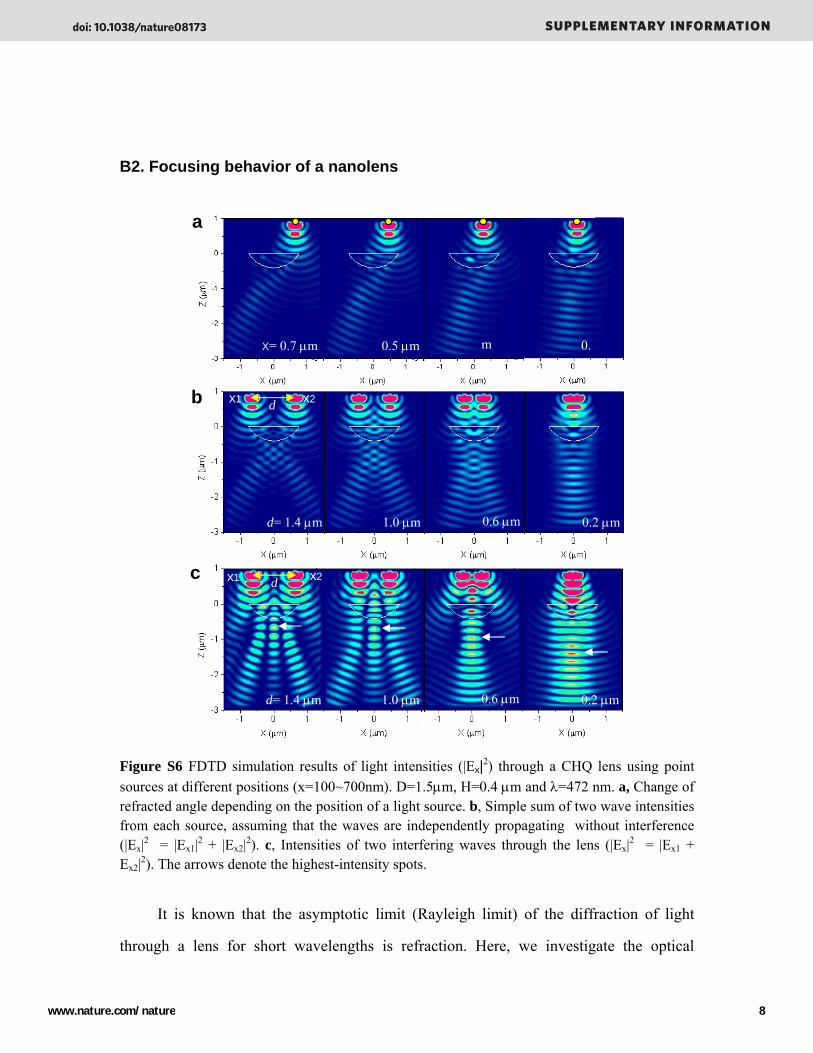
B2. Focusing behavior of a nanolens
Figure S6 FDTD simulation results of light intensities (|Ex|2) through a CHQ lens using point sources at different positions (x=100~700nm). D=1.5μm, H=0.4 μm and λ=472 nm. a, Change of refracted angle depending on the position of a light source. b, Simple sum of two wave intensities from each source, assuming that the waves are independently propagating without interference (|Ex|2 = |Ex1|2 + |Ex2|2). c, Intensities of two interfering waves through the lens (|Ex|2 = |Ex1 + Ex2|2). The arrows denote the highest-intensity spots.
It is known that the asymptotic limit (Rayleigh limit) of the diffraction of light
through a lens for short wavelengths is refraction. Here, we investigate the optical
d= 1.4 μm 1.0 μm 0.6 μm 0.2 μm
b
a
m 0. X= 0.7 μm 0.5 μm
c
d= 1.4 μm 1.0 μm 0.6 μm 0.2 μm
d x1 x2
x2 x1 d
doi: 10.1038/nature08173 SUPPLEMENTARY INFORMATION
www.nature.com/nature 8
properties of refraction and diffraction of the beam-like light sources through the
nanolens (Fig. S6). The single light source simulation (Fig, S6a) deceptively appears to
be a refraction-like pathway at first sight. However, careful analysis shows that the
pathway is much more tortuous than the geometrical ray path. This is due to the fact that
at the interface between the inside and outside of the convex nanolens having extremely
high curvature, the wave path must be strongly twisted to match the phase of the wave
front inside the lens with that outside the lens (Fig. S6a). The beam pathways visualized
along the highest intensity profiles in Fig. S6b shows the case where the intensities of two
symmetric waves are simply added. However, the actual intensity is formed by the
interference of two waves from each source, where each of the brightest spots can be
considered a focal point (Fig. S6c). In this case, the intensity increases due to the
enhancement of the amplitude by superposition (i.e., the diffraction effect), as compared
with the case of Fig. S6b. The focal length tends to be much smaller for the light sources
closer to the edges of the lens. Since the solid angle around the edges is much larger than
that around the center, the focal length obtained by the plane wave is close to the focal
length obtained by the two symmetric sources near the edges. Since this focal length is
much shorter than that obtained by the geometric ray tracing, the focusing phenomenon
by a nanolens is due to the near-field focusing whose origin arises from the stringent
phase matching phenomenon at the interface of a nanolens with extremely large
curvature.
doi: 10.1038/nature08173 SUPPLEMENTARY INFORMATION
www.nature.com/nature 9
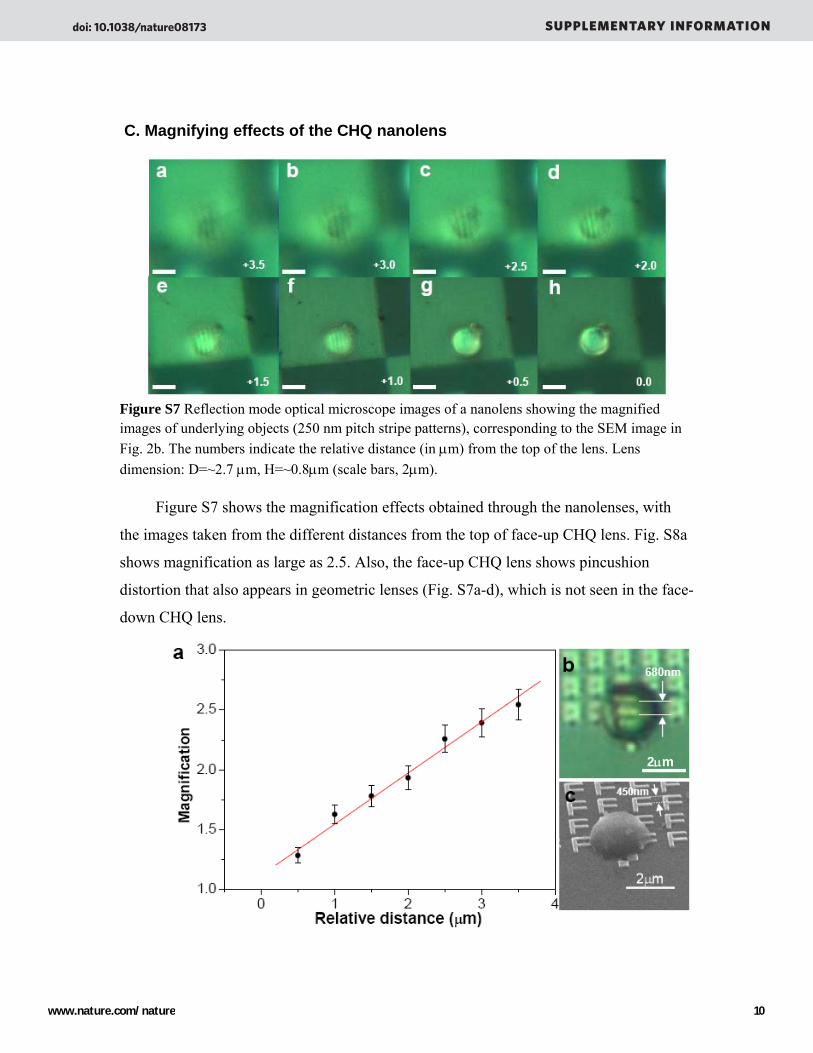
C. Magnifying effects of the CHQ nanolens
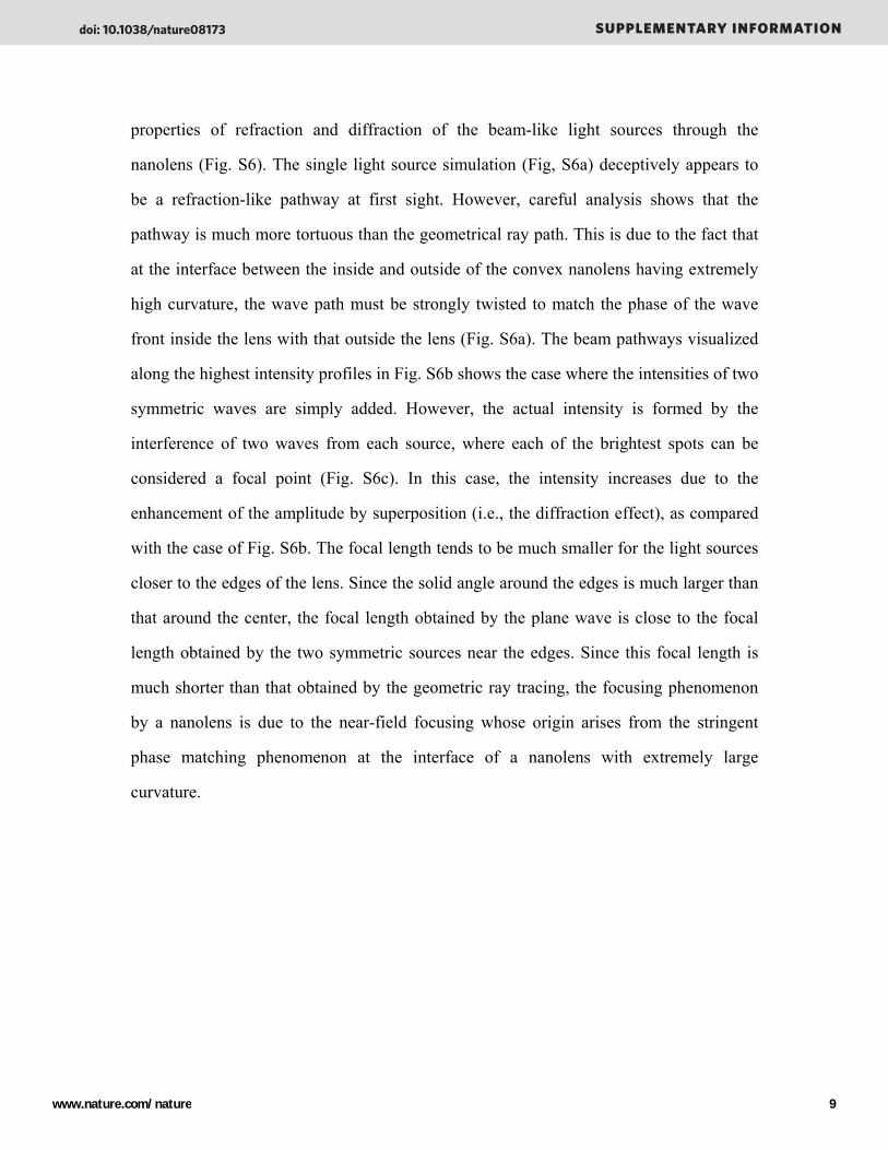
Figure S7 Reflection mode optical microscope images of a nanolens showing the magnified images of underlying objects (250 nm pitch stripe patterns), corresponding to the SEM image in Fig. 2b. The numbers indicate the relative distance (in μm) from the top of the lens. Lens dimension: D=~2.7 μm, H=~0.8μm (scale bars, 2μm).
Figure S7 shows the magnification effects obtained through the nanolenses, with
the images taken from the different distances from the top of face-up CHQ lens. Fig. S8a
shows magnification as large as 2.5. Also, the face-up CHQ lens shows pincushion
distortion that also appears in geometric lenses (Fig. S7a-d), which is not seen in the face-
down CHQ lens.
2μm
doi: 10.1038/nature08173 SUPPLEMENTARY INFORMATION
www.nature.com/nature 10

Figure S8 Magnifying Effects through CHQ nanolenses. a, Magnification with respect to the relative distance from the top of lens obtained from Fig. S5. The error bars denote s.d. b-c, OM/SEM images of the CHQ lens on the ‘F’ patterns. The line spacing looks magnified by ~1.5 through the lens.
doi: 10.1038/nature08173 SUPPLEMENTARY INFORMATION
www.nature.com/nature 11
D. Negative e-beam resist properties of CHQ nanostructures
a b
c
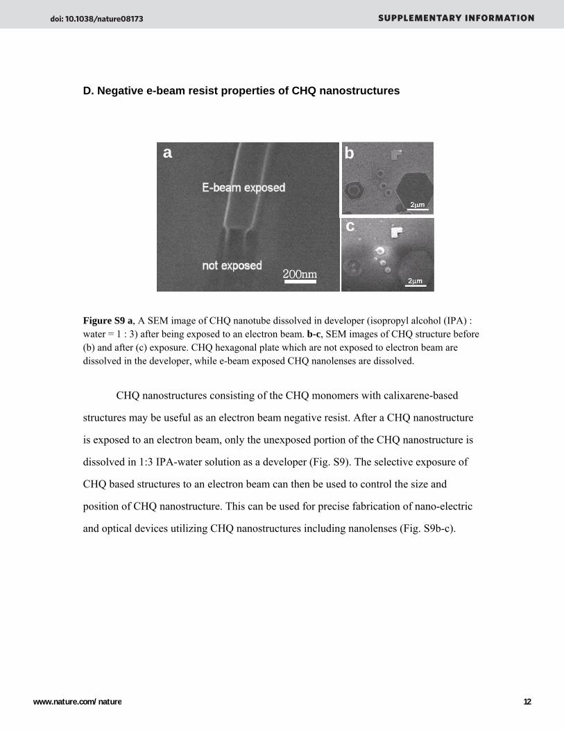
Figure S9 a, A SEM image of CHQ nanotube dissolved in developer (isopropyl alcohol (IPA) : water = 1 : 3) after being exposed to an electron beam. b-c, SEM images of CHQ structure before (b) and after (c) exposure. CHQ hexagonal plate which are not exposed to electron beam are dissolved in the developer, while e-beam exposed CHQ nanolenses are dissolved.
CHQ nanostructures consisting of the CHQ monomers with calixarene-based
structures may be useful as an electron beam negative resist. After a CHQ nanostructure
is exposed to an electron beam, only the unexposed portion of the CHQ nanostructure is
dissolved in 1:3 IPA-water solution as a developer (Fig. S9). The selective exposure of
CHQ based structures to an electron beam can then be used to control the size and
position of CHQ nanostructure. This can be used for precise fabrication of nano-electric
and optical devices utilizing CHQ nanostructures including nanolenses (Fig. S9b-c).
doi: 10.1038/nature08173 SUPPLEMENTARY INFORMATION
www.nature.com/nature 12
E. Relocation of CHQ nanolenses for fabrication
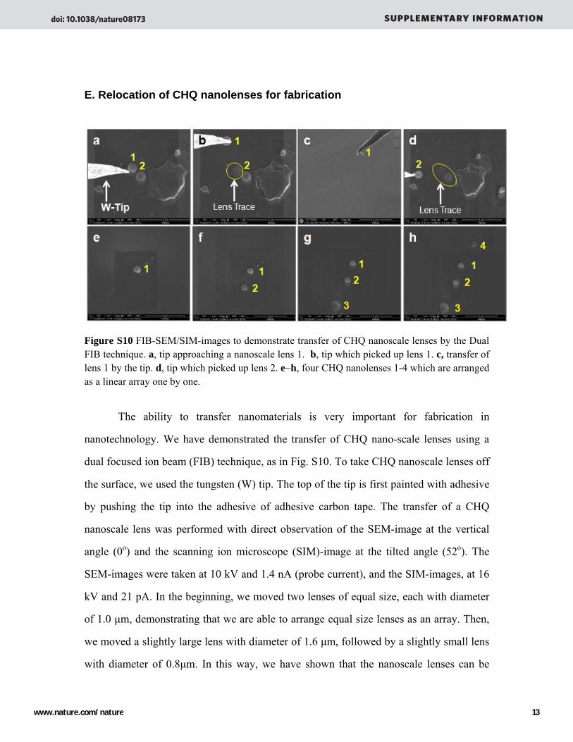
Figure S10 FIB-SEM/SIM-images to demonstrate transfer of CHQ nanoscale lenses by the Dual FIB technique. a, tip approaching a nanoscale lens 1. b, tip which picked up lens 1. c, transfer of lens 1 by the tip. d, tip which picked up lens 2. e~h, four CHQ nanolenses 1-4 which are arranged as a linear array one by one.
The ability to transfer nanomaterials is very important for fabrication in
nanotechnology. We have demonstrated the transfer of CHQ nano-scale lenses using a
dual focused ion beam (FIB) technique, as in Fig. S10. To take CHQ nanoscale lenses off
the surface, we used the tungsten (W) tip. The top of the tip is first painted with adhesive
by pushing the tip into the adhesive of adhesive carbon tape. The transfer of a CHQ
nanoscale lens was performed with direct observation of the SEM-image at the vertical
angle (0o) and the scanning ion microscope (SIM)-image at the tilted angle (52o). The
SEM-images were taken at 10 kV and 1.4 nA (probe current), and the SIM-images, at 16
kV and 21 pA. In the beginning, we moved two lenses of equal size, each with diameter
of 1.0 μm, demonstrating that we are able to arrange equal size lenses as an array. Then,
we moved a slightly large lens with diameter of 1.6 μm, followed by a slightly small lens
with diameter of 0.8μm. In this way, we have shown that the nanoscale lenses can be
doi: 10.1038/nature08173 SUPPLEMENTARY INFORMATION
www.nature.com/nature 13
manipulated. The tip in FIB can be employed to take each nanolens off the surface and
put it at a pre-determined position. Lenses of either uniform size or non-uniform size for
a specific purpose can be selected. Thus, it is possible to make any kind of shapes as well
as arrays. A simple demonstration of an array comprised of four nanolenses, two of
almost equal size, one of larger size, and one of smaller size is provided in Fig. S10. In
Fig. S10d, one can note that the nanoscale lens is on the top of the tip, which indicates
that it would enhance the resolution of aperture-less near-field scanning optical
microscope (ANSOM). Indeed, to demonstrate this more vividly, another experiment has
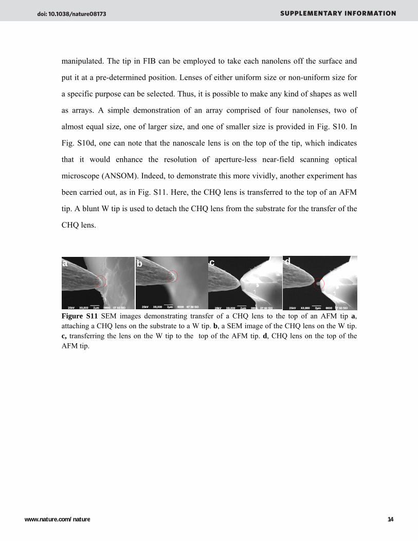
been carried out, as in Fig. S11. Here, the CHQ lens is transferred to the top of an AFM
tip. A blunt W tip is used to detach the CHQ lens from the substrate for the transfer of the
CHQ lens.
d c
a b
Figure S11 SEM images demonstrating transfer of a CHQ lens to the top of an AFM tip a, attaching a CHQ lens on the substrate to a W tip. b, a SEM image of the CHQ lens on the W tip. c, transferring the lens on the W tip to the top of the AFM tip. d, CHQ lens on the top of the AFM tip.
doi: 10.1038/nature08173 SUPPLEMENTARY INFORMATION
www.nature.com/nature 14
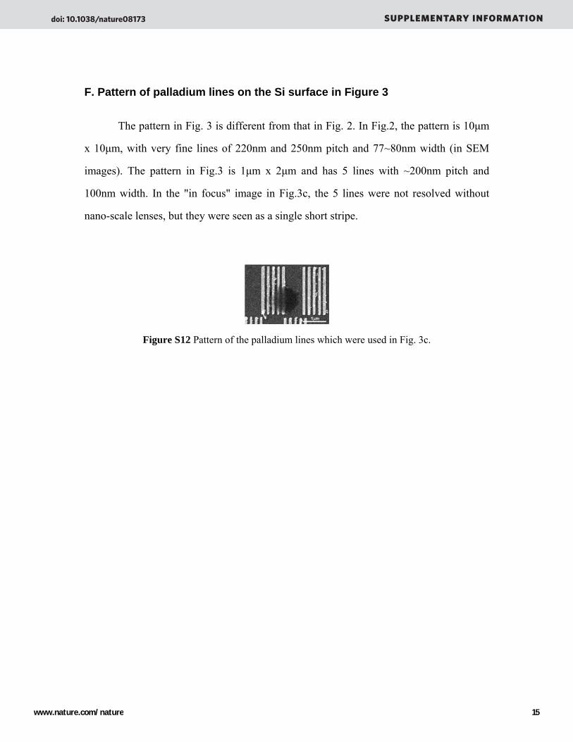
F. Pattern of palladium lines on the Si surface in Figure 3
The pattern in Fig. 3 is different from that in Fig. 2. In Fig.2, the pattern is 10μm
x 10μm, with very fine lines of 220nm and 250nm pitch and 77~80nm width (in SEM
images). The pattern in Fig.3 is 1μm x 2μm and has 5 lines with ~200nm pitch and
100nm width. In the "in focus" image in Fig.3c, the 5 lines were not resolved without
nano-scale lenses, but they were seen as a single short stripe.
Figure S12 Pattern of the palladium lines which were used in Fig. 3c.
doi: 10.1038/nature08173 SUPPLEMENTARY INFORMATION
www.nature.com/nature 15
G. UV lithography using a nanoscale lens
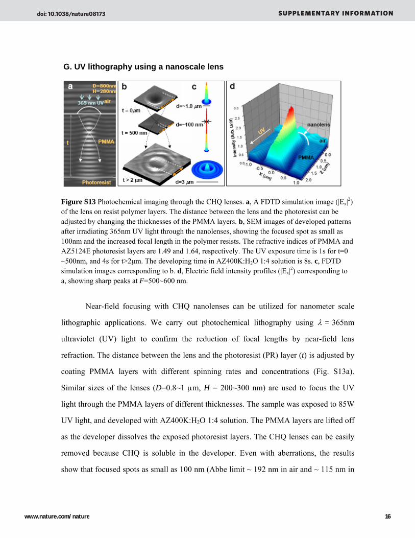
Figure S13 Photochemical imaging through the CHQ lenses. a, A FDTD simulation image (|Ex|2) of the lens on resist polymer layers. The distance between the lens and the photoresist can be adjusted by changing the thicknesses of the PMMA layers. b, SEM images of developed patterns after irradiating 365nm UV light through the nanolenses, showing the focused spot as small as 100nm and the increased focal length in the polymer resists. The refractive indices of PMMA and AZ5124E photoresist layers are 1.49 and 1.64, respectively. The UV exposure time is 1s for t=0 ~500nm, and 4s for t>2μm. The developing time in AZ400K:H2O 1:4 solution is 8s. c, FDTD simulation images corresponding to b. d, Electric field intensity profiles (|Ex|2) corresponding to a, showing sharp peaks at F=500~600 nm.
Near-field focusing with CHQ nanolenses can be utilized for nanometer scale
lithographic applications. We carry out photochemical lithography using λ = 365nm
ultraviolet (UV) light to confirm the reduction of focal lengths by near-field lens
refraction. The distance between the lens and the photoresist (PR) layer (t) is adjusted by
coating PMMA layers with different spinning rates and concentrations (Fig. S13a).
Similar sizes of the lenses (D=0.8~1 μm, H = 200~300 nm) are used to focus the UV
light through the PMMA layers of different thicknesses. The sample was exposed to 85W
UV light, and developed with AZ400K:H2O 1:4 solution. The PMMA layers are lifted off
as the developer dissolves the exposed photoresist layers. The CHQ lenses can be easily
removed because CHQ is soluble in the developer. Even with aberrations, the results
show that focused spots as small as 100 nm (Abbe limit ~ 192 nm in air and ~ 115 nm in
doi: 10.1038/nature08173 SUPPLEMENTARY INFORMATION
www.nature.com/nature 16
oil) are formed with a 500 nm-thick spacer, while a few μm-wide ring diffraction patterns
are formed as the thickness increases over ~2 μm (Fig. S13b). In the case of CHQ
nanolenses in contact with the photoresist layer, ~1 μm-wide and ~500 nm-deep wells are
formed (instead of sharp spots or diffraction rings). This indicates that the focal lengths
increase inside the polymer resists because of the larger refractive index of medium
(nPMMA =~1.5, nPR =~1.6). This result is consistent with the EM wave simulation results
(Fig. S13c,d), though nonlinear effects may also need to be considered to achieve
quantitative agreement. Indeed, such nonlinear effects could be utilized to make a smaller
spot size as the exposing time is reduced.
doi: 10.1038/nature08173 SUPPLEMENTARY INFORMATION
www.nature.com/nature 17
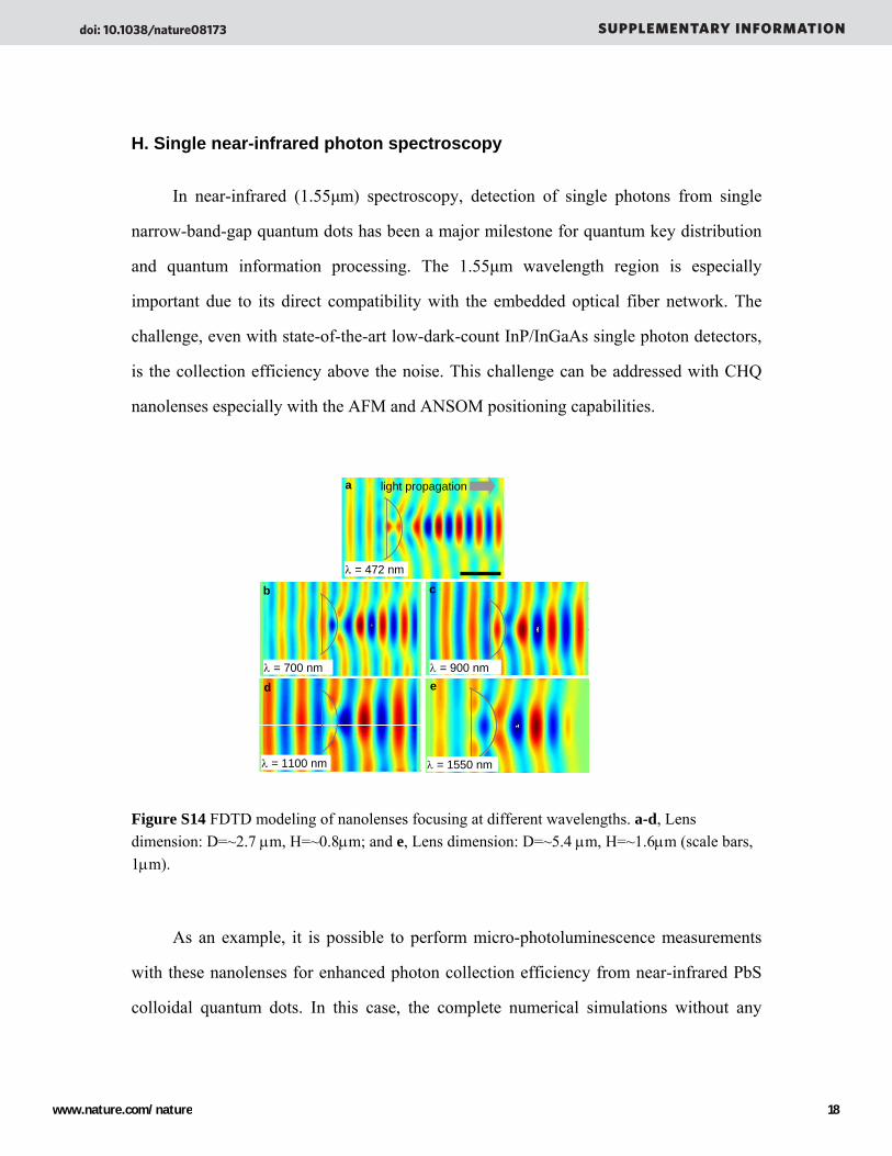
H. Single near-infrared photon spectroscopy
In near-infrared (1.55μm) spectroscopy, detection of single photons from single
narrow-band-gap quantum dots has been a major milestone for quantum key distribution
and quantum information processing. The 1.55μm wavelength region is especially
important due to its direct compatibility with the embedded optical fiber network. The
challenge, even with state-of-the-art low-dark-count InP/InGaAs single photon detectors,
is the collection efficiency above the noise. This challenge can be addressed with CHQ
nanolenses especially with the AFM and ANSOM positioning capabilities.
λ = 1100 nm
λ = 900 nm
c
d eλ = 700 nm
b
λ = 472 nm
light propagationb
λ = 472 nm
light propagationa
λ = 1550 nmλ = 1100 nm
λ = 900 nm
c
d eλ = 700 nm
b
λ = 700 nm
b
λ = 472 nm
light propagationb
λ = 472 nm
light propagationa
λ = 472 nm
light propagationb
λ = 472 nm
light propagationa
λ = 1550 nm
Figure S14 FDTD modeling of nanolenses focusing at different wavelengths. a-d, Lens dimension: D=~2.7 μm, H=~0.8μm; and e, Lens dimension: D=~5.4 μm, H=~1.6μm (scale bars, 1μm).
As an example, it is possible to perform micro-photoluminescence measurements
with these nanolenses for enhanced photon collection efficiency from near-infrared PbS
colloidal quantum dots. In this case, the complete numerical simulations without any
doi: 10.1038/nature08173 SUPPLEMENTARY INFORMATION
www.nature.com/nature 18
approximations (FDTD simulations) in Fig. S14 show that the lens focuses the near-
infrared photons from the dipole emitter into a distinct propagation cone (instead of all 4π
steridians). This can then be matched by the objective of a confocal microscope for
significantly enhanced photon counts, supporting efforts to detect single quantum
emitters at telecommunications wavelengths. The detection of single near-infrared
photons through these nanolenses would be a major advance for scalable quantum
information processes. The nanolens can also help in near-infrared micro-
photoluminescence spectroscopy, where improved collection efficiency is critical.
doi: 10.1038/nature08173 SUPPLEMENTARY INFORMATION
www.nature.com/nature 19
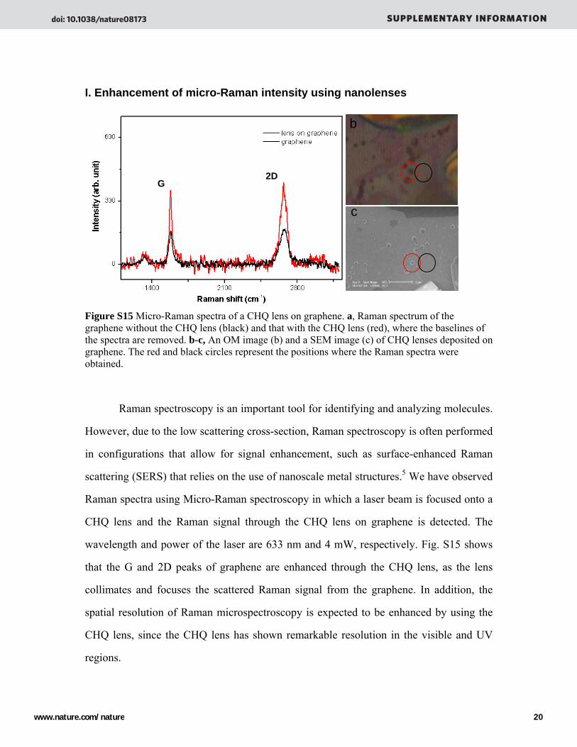
I. Enhancement of micro-Raman intensity using nanolenses
a
2D G
c
b
Figure S15 Micro-Raman spectra of a CHQ lens on graphene. a, Raman spectrum of the graphene without the CHQ lens (black) and that with the CHQ lens (red), where the baselines of the spectra are removed. b-c, An OM image (b) and a SEM image (c) of CHQ lenses deposited on graphene. The red and black circles represent the positions where the Raman spectra were obtained.
Raman spectroscopy is an important tool for identifying and analyzing molecules.
However, due to the low scattering cross-section, Raman spectroscopy is often performed
in configurations that allow for signal enhancement, such as surface-enhanced Raman
scattering (SERS) that relies on the use of nanoscale metal structures.5 We have observed
Raman spectra using Micro-Raman spectroscopy in which a laser beam is focused onto a
CHQ lens and the Raman signal through the CHQ lens on graphene is detected. The
wavelength and power of the laser are 633 nm and 4 mW, respectively. Fig. S15 shows
that the G and 2D peaks of graphene are enhanced through the CHQ lens, as the lens
collimates and focuses the scattered Raman signal from the graphene. In addition, the
spatial resolution of Raman microspectroscopy is expected to be enhanced by using the
CHQ lens, since the CHQ lens has shown remarkable resolution in the visible and UV
regions.
doi: 10.1038/nature08173 SUPPLEMENTARY INFORMATION
www.nature.com/nature 20
J. Supplementary References
1. Hong, B. H., Lee, J. Y., Lee, C.-W., Kim, J. C., Bae, S. C. & Kim, K. S. Self-assembled arrays
of organic nanotubes with infinitely long one-dimensional H-bond chains. J. Am. Chem. Soc. 123,
10748-10749 (2001).
2. Kim, K. S. et al. Assembling phenomena of calix[4]hydroquinone nanotube bundles
by one-dimensional short hydrogen bonding and displaced π-π stacking. J. Am. Chem.
Soc.124, 14268-14279 (2002).
3. Ding, L. & Olesik, S. V. Synthesis of polymer nanospheres and carbon nanospheres
using themonomer 1,8-dihydroxymethyl-1,3,5,7- octatetrayne. Nano Lett. 4, 2271-2276
(2004).
4. Auer, S. & Frenkel, D. Prediction of absolute crystal-nucleation rate in hard-sphere
colloids. Nature 409, 1020-1023 (2001).
5. Hartschuh, A., Anderson, N. & Novotny, L. Near-field Raman spectroscopy using a
sharp metal tip. J. Microsc. 210, 234-240 (2003).
doi: 10.1038/nature08173 SUPPLEMENTARY INFORMATION
www.nature.com/nature 21