Embed Size (px)
Citation preview
A Fie ld- Se que ntia l- Color
1024 _ 768 Liquid- Crysta l- on-
Silic on Displa y
Michael Bolotski and Jean-Jacques Drolet
The Mic ro Display Co rpo ratio n
San Pablo , CA [email protected]
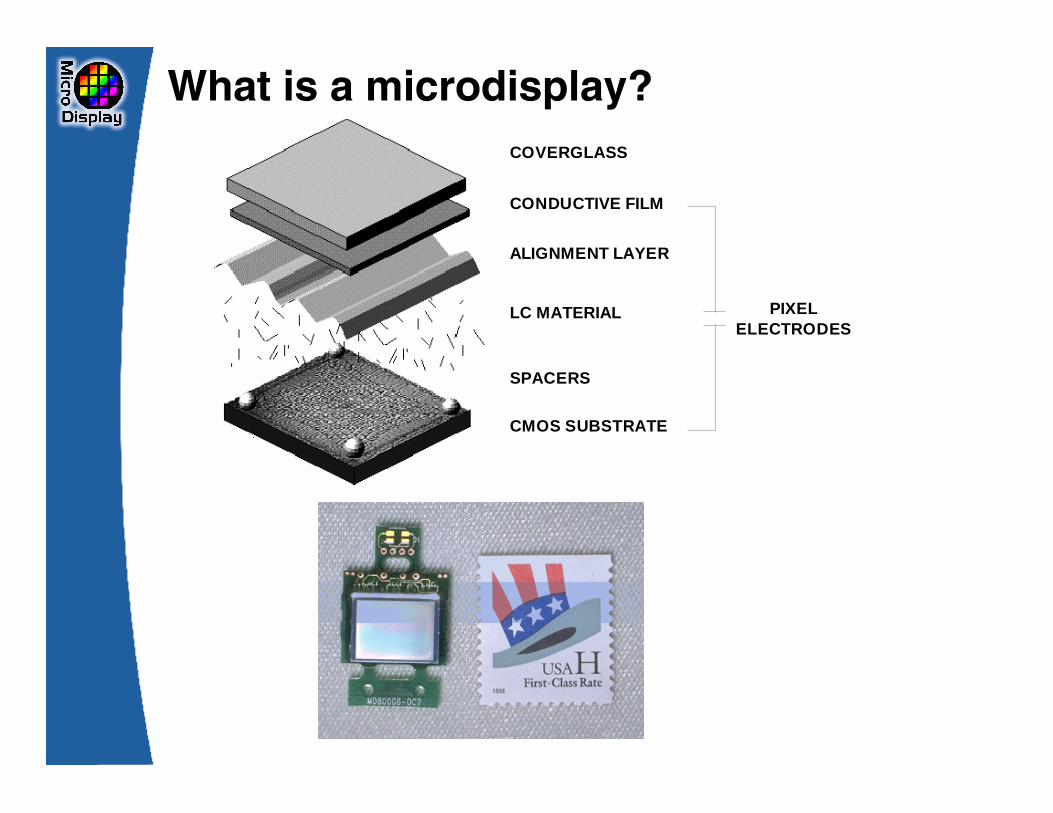
What is a microdisplay?
COVERGLASS
CONDUCTIVE FILM
ALIGNMENT LAYER
LC MATERIAL
SPACERS
CMOS SUBSTRATE
PIXELELECTRODES
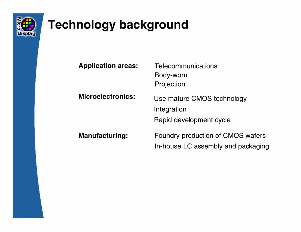
Technology background
Application areas:
Microelectronics:
Manufacturing: Foundry production of CMOS wafers
In-house LC assembly and packaging
Telecommunications
Body-worn
Projection
Use mature CMOS technology
Integration
Rapid development cycle
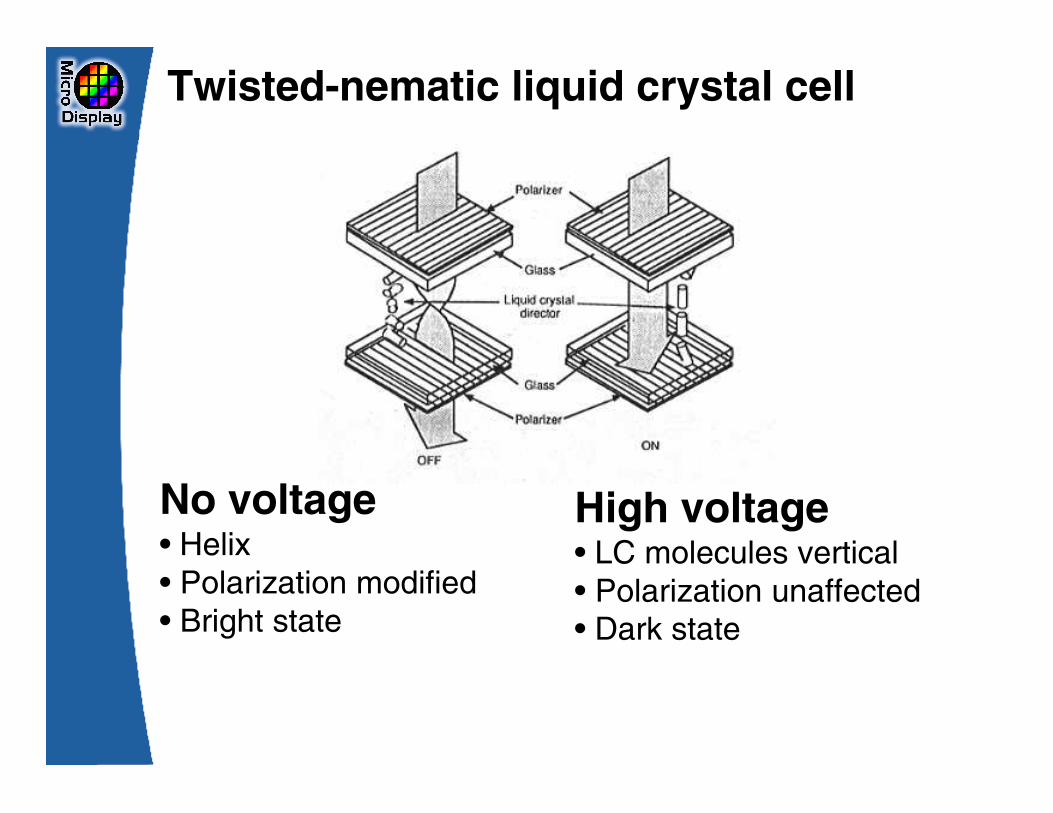
Twisted-nematic liquid crystal cell
No voltage• Helix
• Polarization modified
• Bright state
High voltage• LC molecules vertical
• Polarization unaffected• Dark state
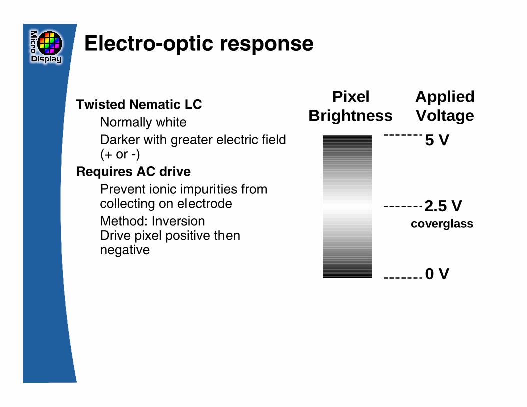
Electro-optic response
Twisted Nematic LC
Normally white
Darker with greater electric field(+ or -)
Requires AC drive
Prevent ionic impurities fromcollecting on electrode
Method: InversionDrive pixel positive thennegative
5 V
0 V
2.5 V
AppliedVoltage
PixelBrightness
coverglass
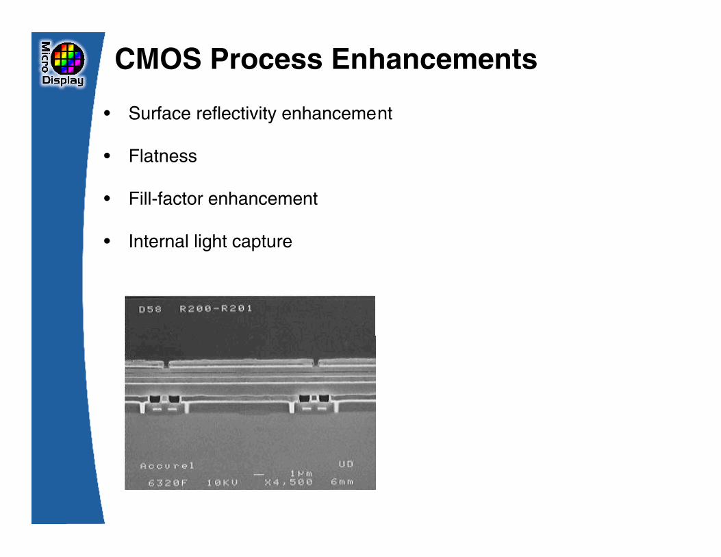
CMOS Process Enhancements
• Surface reflectivity enhancement
• Flatness
• Fill-factor enhancement
• Internal light capture
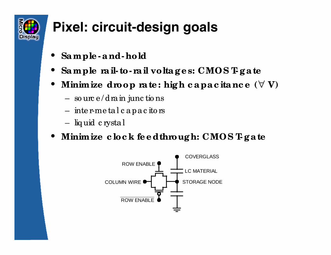
Pixel: circuit-design goals
• Sa mple - a nd- hold
• Sa mple ra il- to- ra il volta g e s: CMOS T- g a te
• Minimize droop ra te : hig h c a pa c ita nc e (∀ V)
– so urc e / dra in junc tio ns
– inte r-me ta l c apac ito rs
– liquid c rysta l
• Minimize c loc k fe e dthroug h: CMOS T- g a te
LC MATERIAL
COVERGLASS
COLUMN WIRE
ROW ENABLE
ROW ENABLE
STORAGE NODE
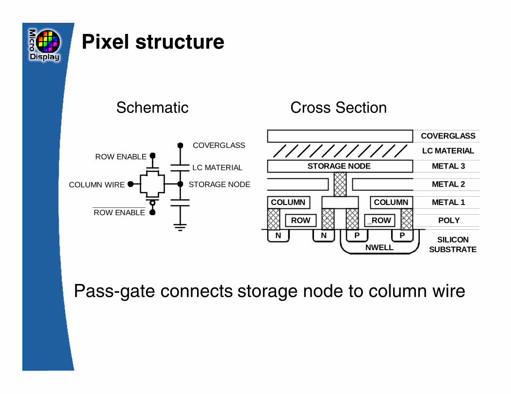
Pixel structure
LC MATERIAL
COVERGLASS
COLUMN WIRE
ROW ENABLE
ROW ENABLE
STORAGE NODE
COVERGLASS
STORAGE NODE METAL 3
LC MATERIAL
METAL 2
METAL 1
ROW _ROW POLY
SILICONSUBSTRATE
COLUMNCOLUMN
NWELL
P PNN
Schematic Cross Section
Pass-gate connects storage node to column wire
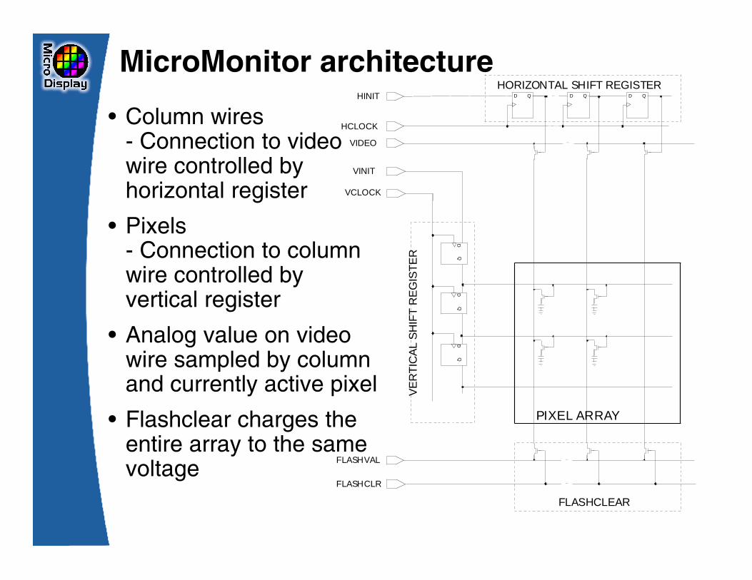
MicroMonitor architecture
• Column wires- Connection to videowire controlled byhorizontal register
• Pixels- Connection to columnwire controlled byvertical register
• Analog value on videowire sampled by columnand currently active pixel
• Flashclear charges theentire array to the samevoltage
QD QD QD
HCLOCK
HORIZONTAL SHIFT REGISTER
VIDEO
HINIT
...
...
...
VINIT
VCLOCK
PIXEL ARRAYV
ER
TIC
AL
SH
IFT
RE
GIS
TE
R QD
QD
QD
FLASHVAL ...
FLASHCLR ...
FLASHCLEAR
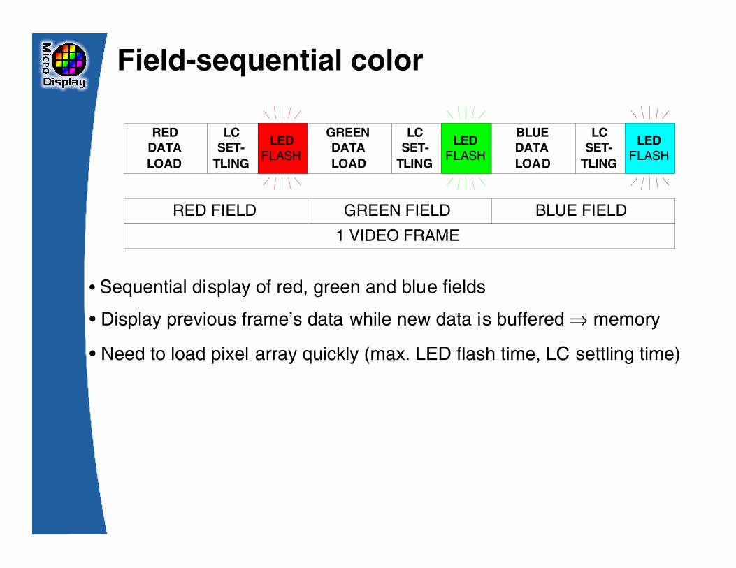
Field-sequential color
RED
DATA
LOAD
LC
SET-
TLING
LED
FLASH
GREEN
DATA
LOAD
LC
SET-
TLING
LED
FLASH
BLUE
DATA
LOAD
LC
SET-
TLING
LED
FLASH
RED FIELD GREEN FIELD BLUE FIELD
1 VIDEO FRAME
• Sequential display of red, green and blue fields
• Display previous frame’s data while new data is buffered ⇒ memory
• Need to load pixel array quickly (max. LED flash time, LC settling time)
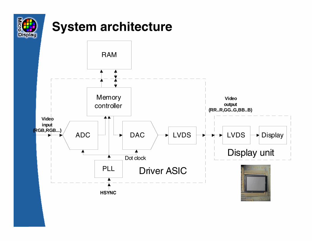
System architecture
ADC DAC
Memory
controller
PLL
LVDS
Dot clock
RAM
Driver ASIC
LVDS Display
Display unit
Videooutput
(RR..R,GG..G,BB..B)
Videoinput
(RGB,RGB...)
HSYNC
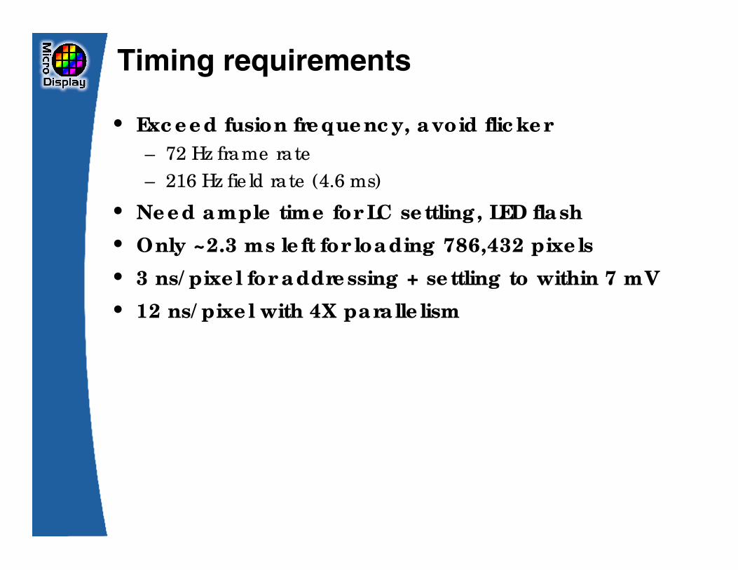
Timing requirements
• Exc e e d fusion fre que nc y, a void flic ke r
– 72 Hz frame rate
– 216 Hz fie ld rate (4.6 ms)
• Ne e d a mple time for LC se ttling , LED fla sh
• Only ~2.3 ms le ft for loa ding 786,432 pixe ls
• 3 ns/ pixe l for a ddre ssing + se ttling to within 7 mV
• 12 ns/ pixe l with 4X pa ra lle lism
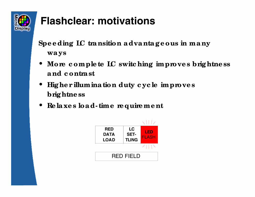
Flashclear: motivations
Spe e ding LC tra nsition a dva nta g e ous in ma ny
wa ys
• More c omple te LC switc hing improve s brig htne ss
a nd c ontra st
• Hig he r illumina tion duty c yc le improve s
brig htne ss
• Re la xe s loa d- time re quire me nt
RED
DATA
LOAD
LC
SET-
TLING
LED
FLASH
RED FIELD
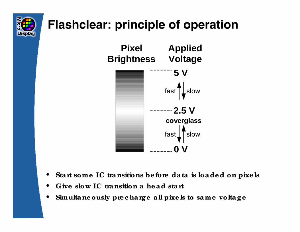
Flashclear: principle of operation
• Sta rt some LC tra nsitions be fore da ta is loa de d on pixe ls
• Give slow LC tra nsition a he a d sta rt
• Simulta ne ously pre c ha rg e a ll pixe ls to sa me volta g e
5 V
0 V
2.5 V
AppliedVoltage
PixelBrightness
coverglass
fast slow
fast slow
Rapid Prototyping Design Cycle
Globa l Wire s
Pixe l De sig ns
Ma nua l Le a fCe ll Editing
DisCo c ompila tion
Ve rific a tion
Global Wires 1: Analysis
Ma thCAD/ Ma ple symbolic a na lysis
De ta ile d pa ra sitic e qua tions
La pla c e e qua tions for distribute d wire s
Symbolic solutions
Pa ra me te r Optimiza tion (Wire R, Wire C, switc h size )
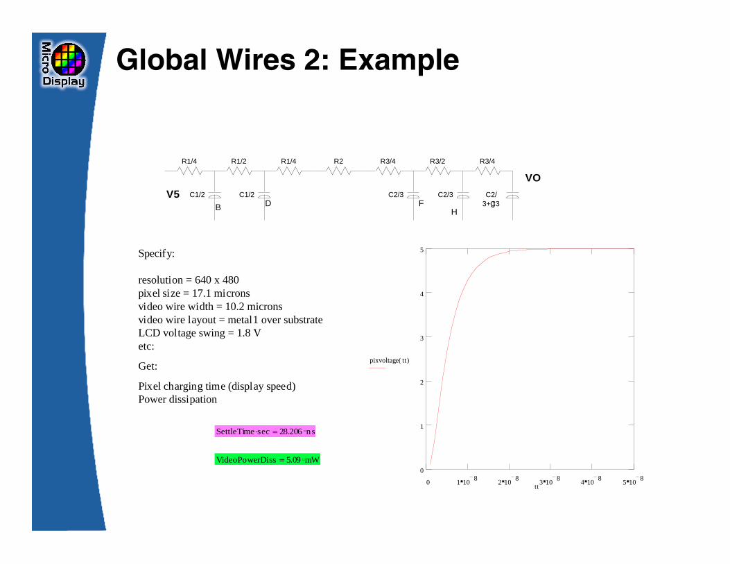
Global Wires 2: Example
pixvoltage tt( )
tt0 1 10
82 10
83 10
84 10
85 10
80
1
2
3
4
5
R1/4
C1/2
R1/2
C1/2
R1/4 R3/4
C2/3
R3/2
C2/3
R3/4R2
C2/3+C3
V5
VO
JH
FDB
SettleTime sec. 28.206 ns=
Specify:
resolution = 640 x 480pixel size = 17.1 micronsvideo wire width = 10.2 micronsvideo wire layout = metal1 over substrateLCD voltage swing = 1.8 Vetc:
Get:
Pixel charging time (display speed)Power dissipation
VideoPowerDiss 5.09 mW=
Global Wires 3: Detailed Simulation
Hspic e tra nsistor le ve l simula tion of distribute d
ne twork
Improve simula tion a c c ura c y to within 3%
c ompa re d to quic k lumpe d a pproxima tion.
Pixel Issues
Photoc urre nt le a ka g e (re ve rse bia s into substra te )
Le a ka g e (pa ss g a te )
Coupling to c olumn wire
Coupling to ne ig hbor pixe l
Stora g e c a pa c ita nc e ma ximiza tion
Yie ld optimiza tion
Pixel Design Process
Fully ma nua l de sig n
Non- a g g re ssive de sig n rule s
De ta ile d pa ra sitic e xtra c tion
Hspic e simula tion of c oupling issue s
Fa bric a te d te st struc ture s
Leaf Cells
All c e lls pe riphe ra l to pixe l a rra y
Exa mple : ve rtic a l/ horizonta l shift re g iste rs, g ua rd
ring s, c olumn switc he s
Most c e lls must be pitc h- ma tc he d to pixe l size
Edits re quire d for func tiona lity or proc e ss mig ra tion,
not for re solution or pixe l size c ha ng e s.
Manual LeafCell Editing
Ha nd- tune d c e lls, full c ustom la yout
De sig ne d for a butme nt, non- ove rla pping
Fe e dthroug h me thodolog y
Re la tive ly fe w c omple x c e lls

Automatic LeafCell Pitch-Matching
Ba se c e ll de sig ne d to minimum pitc h
Rig ht side de sig ne d to be e xte nde d to ma tc h pixe l
pitc h
Automa tic stre tc hing by Displa y Compile r
Stre tc he d c e ll is NOT yie ld optimize d (but is tiny
fra c tion of tota l a re a )
Now What?
Ha ve pixe l la yout
Ha ve g loba l wire pa ra me te rs
Modifie d le a f- c e lls to ma tc h pixe l pitc h, wire size s
Now: pa insta king ta sk of a sse mbling a c hip?
Display Compiler
Constra ine d g e ome try spe c ific a tion
“pla c e bloc k A he re , a lig ne d with top of bloc k B”
Abstra c ts le a f c e lls a s bounding boxe s a nd I/ O
pins
Built on Sc he me prog ra mming la ng ua g e , a llowing
e mbe dde d c ode fra g me nts
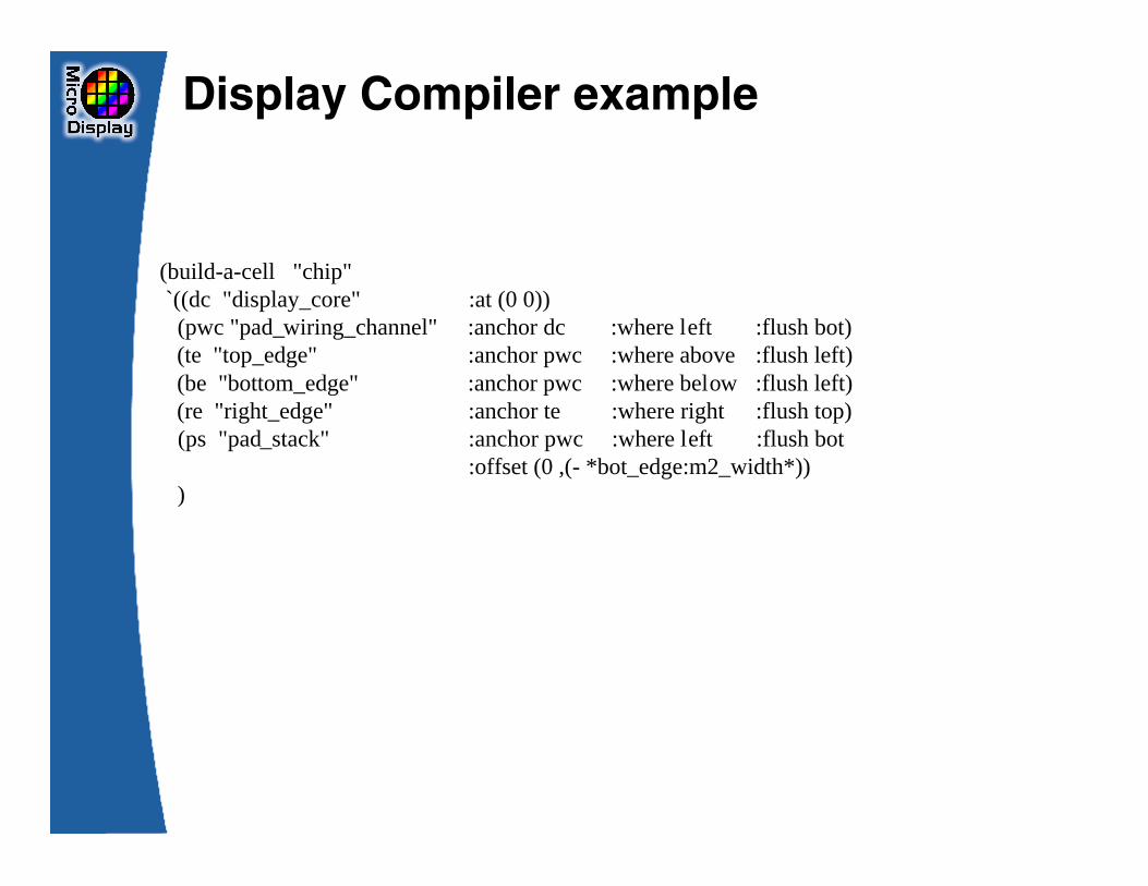
Display Compiler example
(build-a-cell "chip" `((dc "display_core" :at (0 0)) (pwc "pad_wiring_channel" :anchor dc :where left :flush bot) (te "top_edge" :anchor pwc :where above :flush left) (be "bottom_edge" :anchor pwc :where below :flush left) (re "right_edge" :anchor te :where right :flush top) (ps "pad_stack" :anchor pwc:where left :flush bot
:offset (0 ,(- *bot_edge:m2_width*)) )
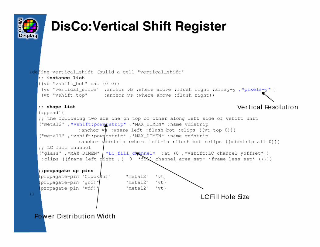
(define vertical_shift (build-a-cell "vertical_shift" ;; instance list `((vb "vshift_bot" :at (0 0)) (vs "vertical_slice” :anchor vb :where above :flush right :array-y ,*pixels-y* ) (vt "vshift_top" :anchor vs :where above :flush right))
;; shape list (append`(
;; the following two are one on top of other along left side of vshift unit("metal2" ,*vshift:powerstrip* ,*MAX_DIMEN* :name vddstrip :anchor vs :where left :flush bot :clips ((vt top 0)))("metal1" ,*vshift:powerstrip* ,*MAX_DIMEN* :name gndstrip :anchor vddstrip :where left-in :flush bot :clips ((vddstrip all 0)));; LC fill channel("glass" ,*MAX_DIMEN* ,*LC_fill_channel* :at (0 ,*vshift:LC_channel_yoffset* ) :clips ((frame_left right ,(- 0 *fill_channel_area_sep* *frame_less_sep* )))))
;;propagate up pins (propagate-pin "ClockBuf" "metal2" 'vt) (propagate-pin "gnd!" "metal2" 'vt) (propagate-pin "vdd!" "metal2" 'vt)))
DisCo:Vertical Shift Register
Pow er Dist r ibut ion Width
LC Fil l Hole Size
Ver t ical Resolut ion
DisCo Features
Pa ra me te rize d to pixe l size , re solution
Loc a l g e ome tric re la tionships usua lly do not
c ha ng e
Conside ra ble de sig n re - use
One c hip usua lly de sc ribe d by 20- 30 pa g e s
Disc o de sc ription se rve s a s doc ume nta tion a nd
de sig n log
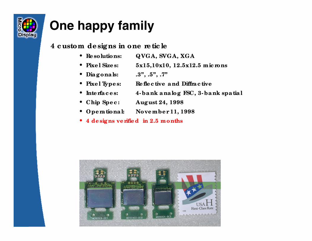
One happy family
4 c ustom de sig ns in one re tic le
• Re solutions: QVGA, SVGA, XGA
• Pixe l Size s: 5x15,10x10, 12.5x12.5 mic rons
• Dia g ona ls: .3”, .5”, .7”
• Pixe l Type s: Re fle c tive a nd Diffra c tive
• Inte rfa c e s: 4- ba nk a na log FSC, 3- ba nk spa tia l
• Chip Spe c : Aug ust 24, 1998
• Ope ra tiona l: Nove mbe r 11, 1998
• 4 de sig ns ve rifie d in 2.5 months


![DX4700HD/DX4800HD Series Hybrid Video Recorder · 2015. 11. 19. · 1024 x 768, 1280 x 720, 1280 x 1024, 1680 x 1050, and 1920 x 1080. The unit supports H.264 (Main profile, [MP]),](https://img.pdfslide.us/doc/110x75/6101fe0fd26847407e3e3e2c/dx4700hddx4800hd-series-hybrid-video-recorder-2015-11-19-1024-x-768-1280.jpg)