Embed Size (px)
Citation preview

Univers
ity of
Cap
e Tow
n
A DIRECT A.C. TO A.C. REGFNERATIVE ___ ... ___ . ----
FRE OU EN CY ft.ND VOLTAGE .CONVERTER
BY
l\~icho.el .Jan1es Case·
Submitted to
THE UNIVERSITY OF CAPE 'rOWN
in fulfilment of the
requ.U~ements for the
degree of
DOCTOR OF PHILOSOPHY
July 1980
' ; - ·, •; . :.·!·. ~;r. ,I

The copyright of this thesis vests in the author. No quotation from it or information derived from it is to be published without full acknowledgement of the source. The thesis is to be used for private study or non-commercial research purposes only.
Published by the University of Cape Town (UCT) in terms of the non-exclusive license granted to UCT by the author.
Univers
ity of
Cap
e Tow
n

Univers
ity of
Cap
e Tow
n
\
ACKNOWLEDGEMENTS
The author wishes to thank -
Professor N.C. de v. Enslin for his help and
encouragement during the course of this thesis ,
Professor L.J.L.N. Besseling for his pithy and
timely words of advice ,
Messrs. M. Attfield and M.N.B. Stephens for
building a large amount of the experimental equipment ,
The University of Cape Town for providing the
facilities to make this research possible ,
Assoc. Professor S. G. Ma.cLaren for his. comments
on the final production of this· thesis,
My wife , Glynne , for bearing with me durin9 the
writing of this thesir:; •
•

.z:rnsTRACT
The reliable variable speed operation of an a.c. machine
over a wide speed range is a problem that has received
attention for some time. In this thesis a system to permit
such operation from a.fixed frequency fixed voltage supply I
is proposed, under the name of the asynchronous modulation
converter. This converter is of the cycloconverter family,
but is fbrce-conunutated and is not synchronised with the
supply frequency. The power switching element comprises a
·power transistor in a diode bridge, coupled to the control
circuitry by opto-isolators.
The output of the a-mod converter is produc.ed by a
"chopper" modulation process and this results in the harmonics
present being at frequencies well removed from the fundamental.
A feedback system to ensure smooth commutation of the out-
put current from the power switches is described. This feed-
back system operates by sensing the rate of rise of the in-
ductive voltage surge on.tl1e load when a switch is opened to
operate a freewheel path switch.

I .
Chapter 1
Chapter 2
Chapter 3
Chapter 4
Chapter 5
Chapter 6
CONTENTS
INTRODUCTION
THE ASYNCHRONOUS MODULATION
CONVERTER
THE ELECTRONIC SWITCH
EXPERIMENTAL REALISATION OF
THE A-MOD CONVERTER
RESULTS OBTAINED FROM THE
EXPERIMENTAL MODEL
A REVIEW AND SOME CONCLUSIONS
REFERENCES
1
13
35
64
78
106
119
. Appendix 1 . OUTPU'r VOLTAGE EXPRESSION 122
Appendix 2
Appendix 3
VOLTAGE DISTORTION FACTOR
INPUT CURREN'r , SINGI,E PHASE
BRIDGE OUTPU'r
Appendix 4 • INPUT CURRENT DISTORTION
FACTOR
Appendix 5 CHARl\CTERISTICS OF THE POWER
TRANSISTOR AND OPTO-ISOLATOR
125
126
129
EMPLOYED 130
Appendix 6 THE BEHAVIOUR OF THE COMPLE'rE
CIRCUI'I' A'J: TURN-ON 137
Appendix 7 -: 'I'HE COMPLETE CIRCUIT BEHAVIOUR
AT TURN-OFF 140

Appendi_x 8 DESIGN DETAILS OF COMPLETE
SYSTEM 142

NOTES ON DRAWINGS
-1) Resistor values are in ohms and capacitor values are in
microf arads
2) Logic symbols are in accordance with DIN practice , as
follows :
NAND Gate
~T-K Flip-flop
Monostable
D Flip-flop CP~

NOMENCLATURE
CL = Load stray capacitance
Ct = Transistor bypass or "snubber" capacitance
C = Supply bypass capacitance sup
· fc = Switching rate
fhI = Input current harmonic frequency
fhO = Output voltage harmonic· frequency
f 1 = Supply frequency
f 0 = Output frequency
ft = Transistor transition frequency
hFE = Transistor forward current transfer ratio
r 1 = Input current fundamental component
= Base current
= Collector current
= Fundamental current
Ih = Harmonic current
I0
= Peak output current
i0
=· Instantaneous output current
iph = Current in one supply phase
Is/b = Second breakdown collector current
j = Any integer 1 , 2 , or 3
k = Boltzmann's constant
= Load inductance , R-L load
= Load inductance L load
= Supply circuit inductance
0

Es = Supply voltage
m = Any integer 1 2 3 etc. , , n = II II II II II
p = Pulse number
q = Charge on an electron
~ = Load resistance
RS = Supply circuit resistance
Rsup = Supply bypass resistance
Sn = Switching function
II
T = Control' pulse frame duration , or transistor turn-off
time ; clear from context
t = Time in general , or in eqn. 3.15 , abs. temp.
VCE = Collector - emitter voltage
VcEO(SUS) = Maximum collector-emitter voltage, base open circuit
VcEX = Maximum collector-emitter voltage, base reverse-biassed
Vav = Mean output voltage
Vi = Peak input voltage
vi = Instantaneous input voltage
v0
= Instantaneous output voltage
w1 . = Su_pply angular velocity
wm = Modulating angular velocity
w0
= Output angular velocity
µ = Input current distortion factor
T = Time duration of switch conduction
• 1 =.Input current phase angle

CHAP'l'ER 1
INTRODUCTION
1.1 A HISTORICAL PERSPECTIVE:
"Now that electric power is so widely distributed on
the three-phase system, there is a distinct ~dvantage in
being able to use an induction motor directly connected to
the mains, instead of a motor that requires the conversion
of the power into direct current··•
The-recent advances that have been made in the econo-
mical·COntrol Of the speed of induction motors have opened
up to the manufacturer and other power users the possibility
of employing this type of motor in cases where its so-called
constant-speed characteristic would, have banned it. as un-
~uitable only a few years ago."
These prophetic words introduce Miles-Walker's book of
1924, "The control of the speed and power factor of induction
motors 11 (l). It is noteworthy that the fi.rst part of the pre-
diction has indeed come true, as the induction motor today
drives a myriad of rotating devices at ratings from a fraction
of a kilowatt to tens of megawatts. The latter part of th~
-
1
prediction has, however, been somewhat tardy in its fulfilmemt,
as the. variable-speed induction motor drive still has a multi-
tude of effective competitors ( 2) ( 4) (10) (13) •
The relative lack of acceptance by users of rotating
machinery of the variable-speed induction motor in comparison
to the widespread use of variable-speed d.c. machines may be

ascribed to various factors. Many of what may be termed the
non-electronic solutions have suffered from a limited speed
range, poor starting torque (in comparison to the d.c.
motor}, low ef:ficiency and, high cost(!). Very often the
machine is purpose-built, like the Boucherot machine, and
is thus only applicable where a special motor would have to
be used in any case, ·like the U.S. Navy battleships of the
pre-war era(l). ·On the other hand, the electronic frequency
converter has been, before the advent of the solid-state
device, an unreliable, costly and cumbersome affair(8). The
mercury-arc rectifier, while being an efficient device,
certainly is not compact, and large-scale use of these for,
say, cycloconversion would only be justified when the need
to avoid a d.c. machine (in say, a Ward-Leonard configuration)
was created by environmental or similar factors(4}.
The tremendous amount of significant research carried.
out during the 1920's ~nd 1930's laid the theoretical
·- foundation which is seeing practical fulfilment during the
present era 6£ the solid-state device. The d.c. drive has
also benefited from modern advances, and, in comparison with
its a.c. counterpart, offers the advantage of simplicity and
hence reliability. 'l'he inherent simplicity of the induction
motor, coupled to the ir1creasj_ng reliability and decreasing
(relative) cost of electronic systems, make the advantages
of the d.c. drive of lesser significance in many applications.
The commutator of the d.c. motor is particularly suspect,
from both a maintenance and environmental hazard point of view.
~hus it is proposed to confine this work to the v~riable
speed induction motor drive, and in particular to an electronic
converter capable of altering constant-voltage constant-f re
quency a. c. into variabl.e-·freguency var:Lable-voltage a. c.
2

Voltage-fed inverter
L
Current-fed inverter
Direct converter
]2.g. 1.1. Induction motor speed control by electronic
stator' frequency '{ariation
'
3

suitable for powering an induction motor.
The methods for achieving this con~ersion are,· broadly
speaking, the d.c. link inverter and the direct converter.
The d.c. link inverter comprises a rectifier, which may or
may not be phase-controlled, with constant voltage or con
stant current output, driving a polyphase inver~er. The
direct converter, which could be a cycloconverter, in one
of many configurations (8) (9) (12) (13), or the asyn
chronous modulation converter which forms the subject of
this work, directly modulates the supply to produce the de
sired output. These possibilities are shown diagramatically
in Fig. 1. 1.
1.2 VARIABLE-SPEED INDUCTION MOTOR DRIVES - GENERAL:
The fundamental principles governing .. the variable-speed
operation of an induction motor are summed up in the
equations 2f
n = s no. poles ( 1. 1)
and
nr = ns (1 - S) ( 1. 2)
From these equations (ref. 5) it can be seen that the speed
of an inducti.on motor may be varied by varying
* Stator frequency
* Number of poles
* Slip
The ingenuity of many designers has been applied to various
schemes to control these parameters, and Fig. 1.2 indicates
diagramatically, but not exhaustively, some of the possi
bilities. It is, however, true to say that the advent of the
solid-state power device (diode, thyristor, transistor) has
4

STATOR FREQUENCY
Voltage-fed inverter {10) (13)
Cyclocon~erter (10) (9) (12)
Current-fed inverter (10)
A-mod coverter (14) (12) (15)
\ Stator ---·
Rotor
-----t Sliprings
POIJE CH.PJ.\IGING : ~----------
SI.IP CON'I'ROL :
Rotor rheostat (1)
Boucherot motor (1)
Motors in cascade (1)
Slip energy
recovery (1)
Leblanc phase
advancer ( 1)
Commutator motors
- N-S
- Schrage (3) (4)
Discrete number pole changes (1) (4) (5) ( 2:1 , 3:1 etc. )
Pole amplitude modulation (5)
Pole stretching (5)
Log motor (5)
Cylindrical rqtor (5)
Fi£.!_l. 2. Induction motor speed control Eossi.bilitie_~
5

tended to put most of these ingenious schemes in the shade
and modern development has tended to focus attention. on the
possibilities of supplying a variable-frequency a.c. supply
to the variable-speed induction motor drive.
It is also, however, a requirement of a variable-fre-
quency system to maintain constant flux in the machine(?) (5).
This is from the property of an inductance,
e -- N-9.2_ dt ( 1. 3)
Thus any variable-frequency scheme must also be capable of
varying the voltage at the terminals of the motor.
The operation of a drive may be considered from the
point of view of its speed-torque capabilities. This is
usually illustrated diagramatically o~ 4 quadrants of
operation as in Fig. 1.3(9). One-quadrant operation is the
simplest to arrange, be it by means .of voltage-fed or current-
fed inverter. '1.'wo-quadrant operation implies the ability of I
inversion, i.e. current direction unchanged but energy return
to mains via reversed potential. Four-quadrant operation
means that the machine may motor or regenerate in either
direction. D.c. link inverters may operate in any mode, the
only determining factor beirig the preparedness of the user to
pay for additional facilities. Four-quadrant operation of
the voltage-source d.c. link inverter does mean that the
rectifier portion of the system must be a dual converter; a
conscious decision must be made to switch between thyristor
banks, in order to supply a reversed-potential reversed-
current output.
The cycloconverter, which comprises a modulated dual
converter, is inherentl.y a 4-quadrant device, but the bank-
selection problem remains a determining factor in design
(8) (9) (10) (12) (13).
6

7
ONE QUADRANT ------~__._~__.,_,_....._......_.+
Speed· OPERATION :
Unidirectional rotation
no braking •
T
TWO QUADRANT OPERATION :
Unidirectional rotation ;
braking •
FOUR QUADRJl.NT OPERATION
Bidirectional rotation ;
braking .
yig. 1.3. Modes of drive operation ~

8
The asynchronous modulation converter, which could be .
classed with the cycloconverter family, avoids the bank
selection problem by force-commutating the switching elements;
use of force-commutation in the normal cycloconverter would -
also solve this problem(12) (14) (15).
1.3 THE D.G. LINK INVERTER:
The d.c. link inverter, as previously mentioned, corn-
prises a rectifier coupled to a d.c. to a.c. converter. The
two main types are the voltage-source(27) inverter and current
-source converter(25) (26). Briefly, the voltage-source in-
verter produces a constant d.c. voltage from a (usually)
phase-controlled rectifier. If the inverter is to operate in
4 quadrants then the rectifier comprises two back-to-back
thyristor banks to enable regeneration to take place. Thy-
ristors are used on equipments of larger sizes and these have
to be fast-turn-off "inverter grade 11 devices.
The output waveform of the voltage-source inverter is
not a pure sinusoid and various attempts have been made to
reduce the distortion(28). Triple-n harmonics are eliminated
by the 3-phase connection, and reduction of 5th and 7th
harmonics is quite feasible. It is thus possible to operate
an induction motor over a wide speed range; even down to
standstill.
The disadvantages of the voltage-source inverter are
serious. These are
High speed thyristors must be used.
Complex ci~cuitry required for regeneration.
Forced commutation of inverter thyristors is
prone to failure. This leads to unkind remarks
like "An equipment only microseconds from
failure 11 ! (26)

"' The current-source inverter, on the other hand, com-
prises a phase-controlled (full bridge) rectifier supplying
a constant current (via a large inductance) to a force-com
mutated thyristor inverter(25) (26). · The commutation cir
cuitry is considerably simpler and "rectifier grade" thy
ristors may be used. Since the current flow is undirectional,
regeneration is obtained when the rectifier goes into the
inversion 1node of operation, avoiding the bank selection
problem.
The main disadvantage of the current-source is the
erratic behaviour of the motor at low speeds, due to the
current waveform that must perforce be impressed on the
machine ( 29) •
The disadvantages listed for both classes of inverter,
while not being entirely inhibitory to the use of these
systems, are sufficient to hamper the fulfilment of Miles
Walker's prophecy. The d.c. drive suffers from few similar
disadvantages, on the other hand, and would account for the
continued "popularity" of it.
1.4 THE CYCLOCONVERTER:
The cycloconverter performs a direct a.c.·to a.c. fre
quency conversion - that is, there is no d.c. link in the
circuit. Fig. 1.4 shows how two converters {rectifiers) may
be connected to provide a single-phase output. These two
converters connected in parallel comprise a dual converter.
9
The control signal controls the firing angle of each converter
in order to produce half-sine outputs which are summed to pro
duce a sinusoidal output. The usual electronic control devices
used in the dual converter are thyristors(9); since there is

2 INV.
L
detector
Output
I 1RECT.
CONTROLi--~~~~--
Set speed
1 INV.
2 RECT.
Conv. 2
·. I
2 INV.
Fig. L 4. Basic cycloconverter operation ! Bank selection
£.y_current detection or cir_5:ulatj_1:.9-:__£~_E_ent limited
10

no intrinsic turn-off capability care must be taken to avoid
a short-circuit between converters (or thyristor "ba1.1ks") .
Fig. 1.4 indicates some possibilities. ~f the tapped in
ductor L is used for current-limiting then both converters
may conduct simultaneously and the cycloconverter operates
11
in the "circulating current" mode(9). If the current-zero
detector is used then bank selection may take place under its
direction; various control strategies may be adopted, such as
"first current zero" or "fundamental current zero" (9) (12) (13.).
Since the control signal continuously varies the firing
angle, the output voltage and input current harmonics are not
simple functions of output frequency and voltage separately,
but functions of both(9) (12) (30). Especially troublesome
are subharmonics in the supply line current.
'I'he corrunutation problem poses difficulties for high fre
quency operation of the cycloconverter and generally the use
of these systems is confined to low-frequency systems operating
below 1/3 of supply frequency. The large nuwber of components
is also considered a disadvantage, but this disappears at high
power drives(31).
If the use of a force-commutated switching element is
postulated, then·the classical cycloconverter acquires a new
appearance. It j_s then possible to operate with unity or
controllable input displacement factor, minimum output voltage
distortion or unrestricted input-to-output frequency ratio.
These possibilities are dealt with in refs. (12) and (13). The
unrestricted frequency changer (U.F.C.) in particular is very
interesting as this system overcomes some of the objections to
the cycloconverter.
The asynchronous modulation converter which forms the
subject of this work is an extension of the cycloconverter

concept; in particular of the U.F.C. By using a switch with
intrinsic turn-off capability and by operating with a higher
modulation frequency it is possible to overcome most of the
problems associated with cycloconverter operation, in parti
cutar the bank selection, input current harmonic and output
voltage distortion problems.
12

13
CHAPTER 2
'Jr!E ASYNCHRONOUS MODULA'I'ION CONVERTER --~-~~~-I
2.1 ------BASIC PRINCIPLES AND CIRCUIT CONFIGURATION:
The basic principle of the a - mod converter is
shown in fig 2.1, which depicts a rotary switch
coupling a load successively to the supply phases.
E
hE
Fig.2.1 . Basic a-mod.convert~ --~
The switch wiper would rotate at a ~teady speed,
applying the load to each supply phase fat an equal
length of time~ The waveform which would be
produced by this arrangement is shown in fig. 2.2.
Time--~
t:.' • 2 ? T,1avef or:m P. r.oduced bv. basic convert?::.:~ _::_.;1g • ·--·-·-~_._n__ . ~

This arrangement only provides for frequency control, , '
with a ·fundamental output frequency.of (Appendix' 1)
'f + c - -·p ( 2 .1)
The ± signs indicate a frequency increase or decrease
depending on whether the direction of rotation of
the switch is the same as the phase rotation
of the supply, or opposing it.
The arrangement shown above thus produces an output
voltage wave by successively switching the input
waves. A more realistic approach would be to
replace the "rotary switch" with a number of
bidirectional electronic switches, one to each
supply phase. The output wave then would consist
of segments of the input waves, with the length
(in time) of each segment depending on the duration
of the closure of the relevant switcho If we refer
to the duration of a pulse sequence of S pulses
(that is, one pulse to each of S switches) as a
control pulse frame of time ~' then the duration
of each input wave segment may be varied by
varying the duration of each control pulse during
the relevant ~ time slot of time T
value of the output voltage is then:
/
v av = 1 m ...
"[
f v dt = 0
0
't' -v T o
The mean
( 2. 2)
The average value of the output wave voltage may thus
be varied by .this process, used in the co~trol of
( .
14

15
DoC drives and known as pulse width modulation.(2,3,10,13)
The relevant pulses are shown in fig. 2.3, and the
circuit configuration for a 3 pulse system
supplying a single~phase load is shown in fig. 2.4.
The usually-accepted symbol for a triac is used
here to denote a bidirectional switch with intrinsic
turn-off capability.
Note that in this thesis the pulse number of a
system is defined as "the nUinber of discrete
phase - related A.C. sources available for the
fabrication of the output wave", in place of the
usually accepted definition which' is "the number
of discrete segments of the output wave which are
fabricated during each cycle of the A.C. input
wave". Since it is proposed ultimately to fabricate
an output wave from many segments the classical
definition is not entirely relevant, since it is
really meant to apply to naturally-commutated
systems. ( 8)
2.2 THE FUNDlJ'.1EN'l'P..L THEORY OF THE A-MOD CONVERTER. ~~~~~~~~---~~--~~~~~-~~~~~ . .._.....-.--
The fundamental theory of the a-mod converter is
obtained by using a similar process to that used
to derive the basic expressions describing the
operation of the cycloconverter. This consists
of multiplying the input wave by a switching
function which describes the operation of the
switches~ This process is shown schematically
in fig~ 2.5.
'

~ Conl~ol Pulse Frame. S '"I
.__ _______ __,fimeslot ._ ___ _
Control pulses to any one switch
r- ~
·I T
Output of switch
Time----1 ...
Fi~ •. ~.3. Ccintrol eulses for pulse width modulation
'\--·
·Freewheel switch
P1 ~
P2 o----<" ...t------111--e---t ~.,_--oNeutral ---..J
Fig. 2.4. 3-Pulse circuit·'configuration
The freewheel or shunt switch provides current
continuity during the supply off time • An open
circuit , in the case of an inductive load ,
would produce destructive voltage surges •
16
',

17
x r l INPUT SWITCHING
FUNCTION
"
OUTPUT
Fig. 2.5. Deriving the output expression
The following assumptions are made, which are usual
for converter and cycloconverter analysis, and
are valid in the case of the a-mod converter: (8,9,10,12)
i) The supply wave is a pure sinusoid from a zero
impedance source. The assumption is made for
the basic derivations, but it will be shown
further on that source impedance has an important
effect on the corrunutation process in the switches~
ii) The output current is a pure sinusoid at the
desired output frequency f0
•
This assumption is justified if the load comprises
some device which only permits current to flow
at fundamental output fre~uency. Since the
demand for power frequency conversion is mainly
in the field of motor speed control the inductive
nature of the usual. load~ postulated prevents

18
significant harmonic current from flowing. It
will be shown that the output voltage harmonics
are at frequencies very much higher than fundamental
.output frequency.
2.2.1 SINGLE PHASE OUTPUT VOLTAGE (Appendix Al)
--The control pulses, which fonna 3-phase switching
function may be expanded by the usual Fourier series
to yield the following expression: (16)
8 n(w.t,w t) . J. 0
= T + ~ T n7T
n+oo n n,... . 'E sin(··r-r ) .cos{n(w.t + w t -
J. 0 n=o 2 ... -(j-l)T >}
The ouput voltage is the product of the control pulse
and the input wave, by analogy to the familiar
"chopper" amplitude modulation process.
Now
Thus
And
v = Vicos { wit - (j-l)~II } i
v ::; Sn ( w. t, w t) x v. 0 J. 0 1
3V. m+oo
sin(3m + l ) .!!..!. --
( 2. 4)
( 2. 5)
. . . . . ( 2. 3)
VO -· J. E ..... T {
TI + - -{ cos m=o
+ 3mw.t + ( 3m l)w t }} J_ 0
~3m 1)
(2.6)
Note that the + signs indicate that the swrnnation
must be repeated for + and - signs.
For a 3-pulse system, referred to the supply neutral,
wh~ch corresponds to the midpoint rectifier system, ,
the fundamental output voltage is:
vol == • TIT
sin-T . cosw t . 0
(2.7)

The maximum value of this expression occurs when:.
1 X T '[ = p
Or
'[ = lT 3
Thus
volmax = 3/3vi t
2II cos WO ( 2. 8)
Or
volmax = 0,827Vi cos WO t (2. 9)
The pulse number may be extended to higher multiples
of 3, in which case a transformer is needed, and then:
2pV. m~oo sin(mp + 1) l!!. - , .. , + .vo = . 1 ~ T { {mpw.t + (mp -· l)w
0t - cos
II m=o (mp + 1) . . 1 -( 2 .10)
As is apparent from equations 2.5 and 2.9, the output
voltage is a function of the ratio of the conduction
period T to the control pulse frame time T. At
E.!. maximum output voltage, T is unity. That is,
the conduction pertdd fills the entire slot allocated
to it. This quantity ~ T is referred to as the
"control ratio". Using ~his definition means that
the maximum output is obtained at a control ratio
of unity, and zero output when it (the control ratio)
. is zero. The midpoint converter has the disadvantage
that a component of the output current flows in the
input. This is overcome by the bridge converter
shown in fig. 2. 6, in single phase form. ( See para.
2.2.4 p. 27 ) •
19
} }

20
Supply o--~-~-~---fll1--~~r--~~-~-~~-r-~--.
phases
Fig. 2.6. Single phase bridge configuration
The output voltage is then:
v = 0
2pV. J.
II
~~00 sin(mp + l).!!.!_
m==o ____ + ____ T_{ .cos· {mpwi t + (mp + .1) w0
t } }
('mp 1) (2.11)
The laboratory-tested model was a 6-pulse bridge
converter, which yields a fundamental output
voltage:
( 2. 12)
And
3V. v . = J. cos w t olmax ·rr-· o
= 0,955V. cos w t l. 0
( 2 • 13)
And if we extend the system to say 12 pulses, using
a transformer,
v = 12Vi sin IT cos w t olmax 12 o rr
( 2. 14)
( 2. 15)
Note that the fundamental frequency occurs when m
is zero~

21
:9
i8
i7
;6
!~
. (LI ~4 ·u
:::> ~
E ;3 0
+-·c: .2 :::>
L.. (LI
a.. ,1
0
-.1
-.2
-.3
Fig:. 2. 7 (a) . 3-Pulse harmonic _amplitudes
,5
,4
(LI ,3 "O :::> ......
E .2 0
...... 'E
.1 :::> '-(LI
0...
- .1 .1 .2 ,3 ,5 ,6 ,7 .e .9 1.0
-.2 r
Pig. 2. 7 ·(b) ~ 6-Pulse harmonic ampli tu.des ------- -- I

2.2.2 OUTPUT VOLTAGE HARMONICS:
Unlike the naturally commutated cyc1oconverter, the
harmonics present in the output voltage of the
a-mod converter obey a simple relationship as shown
in equation (2.~). That is, the relative amplitude
of a given harmonic is a function of the pulse ratio
'(
if only, and not of output frequency. Also the
frequency of a given harmonic is a function only of
input and output frequencies. Note that the
word 'harmonic' is used rather loosely
here, since the usual meaning of the word applies
to simple multiples of some fundamental frequency,
whereas in this text the !harmonics" have a
frequency (from eqn. 2.5) of:
+ = mpf i + (mp 1) f0
I
( 2. 16)
Since however it is customary in current literature
to term the higher multiple frequencies of converter-
like devices "harmonics", the use of the term is
considered justified in this instance.(8,9,l0,11,12,13)
The relationsh:Lp between voltage n:-;duction ratio,
harmonic amplitude and harmonic frequency is illustrated
graphically in figs. 2.7 (a) and 2.7 (b), for the 3
pulse and 6 pulse cases respectively.
The harmonics are of relatively high frequency, the
lowest possible being from a 3 pulse converter with
D.Co output when the first harmonic to appear occurs
at 150 HZ 0
22

These are thus easily filtered, or in the case of \ '
an induction motor output, have litt~e effect on
motor performance. (7)
However, at small voltage reduction ratios i.e.
low output voltages, it is observed that the
amplitude of the harmonics is nearly the same as
the fundamental frequency. This naturally sets a
limit to any filter design, but, as noted above, the
wide frequency separation eases the requirements of
such a filter. In the case of an inductive load
or induction motor load, the harmonic currents ,
are reduced in the ratio:
(2.17)
'I'hi.s usually represents a considerable reduction.
OUTPUT VOLTAGE DISTORTION: (Appe1}dix A2)
Since the output voltage contains unwanted frequency
components, distortion is present and a means of
evaluating this distortion is the distortion factor,
defined as: (9)
R.M. S .• fundamental Voltage distortion factor -· ~-ut ~oltas:e __ _
R.M.S. total output voltage
For a 6 pulse bridge conf igura.tion, the maximum value
of voltage distortion factor is 0,955, and for a 3
pulse midpoint system the corresponding value is 0,826.
23

1.0
0,9
0.8
.... 0,7 0 .. ~
u & c 0,6 0
:.;::: .... 0 0,5 ..... VI
0 (]) 0,4 0 ..... 0 0.3->
0,2
0.1
0
0,9
0,8
'-- 0,7 0 ..... u 0
LL 0.6- -c
0 :.;::: '-0 0,5--+--VI
0 <IJ 0.4- -Cl ..... gl 0,3-
0,2 -
0,1
0
24
t -t· I I I 1---· I I ·-0,1 0,2 0,3 0,4 0,5 0,6 0,7 0,8 0,9 to
Control Ratio
Fig. 2.B(a). 6-Pulse bridge distortion factor
! I ! ,-, -----~1""'. ---i -----1--""i -r-Q1 0,2 0,3 0.4 0,5 0.6 0,7 0.8 0,9 1.0
w 0
The maximum values are reached at maximum control
pulse duration, and fig. 2.8 (a) an~ 2.8 (b) show
the variation of voltage distortion factor for 6
pul$e and 3 pulse systems, respectively. . ,
2.2.4 INPUT CURRENT PER SUPPLY PHASE! SINGLE PHASE
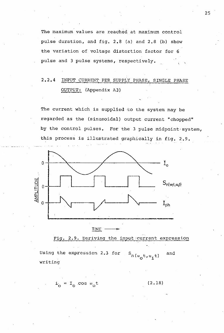
OUTPUT: (Appendix A3)
The current which is supplied to the system may be
regarded as the (sinusoidal) output current "chopped"
by the control pulses. For the 3 pulse midpoint· system,
this process is illustrated graphically in fig. 2~9.
~ 0-·~-_J
CL 2: <{ 0--+----'
Tlt-.IE ---t:--
Fig. 2.9. Deriving the _input:current expre~_s:i.on
·. Using the expression 2.3 for s n(w t,w.t)
0 J.
and
writing
i- == I cos w t 0 0 0
(2.18)
25
26
we have:
2I0
m-+oo + T
~I0cosw0t E sin(mp ·- 1)--
i = +- T {cos{ (mp :!: l)w.t +mpw t}} ph 1f m=o + J. 0
(mp - 1)
( 2. 19}
For the 6 pulse bridge system, the control pulses
are effectively modified by the circuit configuration
in the manner shown in fig. 2.10: r-;·-----
i I
o-----
0
o-----.. -·:.-· '·"
---~·Control Pulses
-Iph
Fi_g. 2.10. Effective 6-pulse bridge control pulses
This process is like that occuring in' the standard
bridge converter and cycloconverter systems.
The switching function then becomes:
( + l).!f..l sin mp T
(mp + 1) {cos(mp ± l){wit + w0 t + i}}
:(2. 20)
Using the previous expression for output current, the
input current per supply phase is:
i =2[310 m+oo
sin(mp -!- l) 2!...I + - + . ' (!QE-1) 1f'} E 'I'
ph-- {cos{ (mp - l)w.t + mpw0
t + · 6 1 m=o -f ... J. 1f (mp - 1)
(2.21)

27
The following are to be noted concerning the input
current:
1) .The midpoint converter has a component of current
at output frequency, which does not occur in
the bridge configuration. This process occurs
in other converters, and is an advantage of the
bridge configuration.
2) The harmonics are never integral multiples of
the pulse number and supply frequency, and the
amplitude of an harmonic is only a function of
harmonic number.
3) The phase angle + (mp - 1) rr - 6 occurs because of the
delta connection of the system, while the control
pulses and supply voltages are referred to the
supply neutral, as in a star connection.
4) The current harmonics are never at the same
frequency.at the (output) voltage harmonics,
having a frequency
+ = (mp l)fi + mpf0 (2.22)
whereas the voltage harmonics occur at a frequency
+ f ho = mpf {'!-(mp 1) f 0
(2.23)
5) The pulse nurnper p becomes unity when considering
a single supply phase, with the-':! proviso that the

quantity mp is never an odd multiple of three~
This has the result that an harmonic of large
amplitude may be expected at a frequency
m is unity.
2o2.5 INP~~-CURRENT PER SUPPLY PHASE, 3 PHASE OUTPUT:
Three single phase converters may be combined into
a.three-phase output device as' shown in fig. 2.11. !~-~---·-------· -·
i I Supply 0--.--1-.----~-+--1--.-----q.-+--t-fl._----,
Phases ,.._~-l...-l--&~-~,___j-~1--~~~--o-~-.--+--1--·-t--t~~---,
Converter 1 Converter 2 Converter 3
. -~-- ·-·- ---·-·· ..... -- --·~~------- ------- ------··-~-··
Fig. 2.11. Three-pha~~ bridge converter
28
Each converter operates independantly and their outputs
are combined within the load, usually a 3 phase
A.c. motor.
The current per supply phase is then
. 6,fn · m-+oo sin(mp + l)~ l. = 0 -ph L: T {cos {(mp + l)w.t + mpw
0 t 1T -m=o + 1 (mp - 1)
(2.24)
The pulse number now becomes three, and the harmonic
at (w. + w ) , associated with the single bridge 1 0
converter, disappears.
+ (mp-~ 1) TI 1 } + 6 -

INPUT CUR~E!_PISTORTION FACTOR (Appendix A4)
The distortion factor of the input current waveform
is given by
\J =
=
R.M.S. fundamental input current
R.M.S. total input current Ii ! r.m.s.
(2. 25)
The 3-pulse midpoint converter with single phase
output has a maximum value (of current distortion
factor)
\J = 0,68
The variation in current distortion factor for the
3 pulse midpoint converter with control pulse
duration is shown graphically in fig. 2ol2.
0,6
0,1
0 0,1 · 0,2 0,3 0,4 0,5 0,6 . 0,7 0,8 0,9 1,0 Control Ratio
Fig. 2~12~ 3-Pulse current distortion factor
The 6 pulse bridge.converter, with single phase
output, has a maximum current distortion factor of
)l = 0.95
29
.,

30
The variation in current distortion factor, for the
6 pulse. bridge converter, with control pulse duration,·
is shown graphically in fig. 2.13
0,9
'- 0,8 0 ......
0,7-u 0
LL c 0,6
.Q ...... 0,5 '-0 ...... Ill 0,4 0
...... 0, c CJJ '-
0. L-::J
(_)
0,1 --I I I I-
0 0.1 0,2 0,3 0.4 0,5 0,6 0,7 0,8 0,9 1.0 Control Ratio
Fig. 2.13. 6-Pulse bridge current distortion factor
For 3 phase output systems, only the 6 pulse bridge
converter will be considered as this is the only
system likely to be of use in the operation of say
a 3 phase induction motor. Fig.2.14 shows how
the three converter supply currents are added.
0 nIL_ ' ~ Iph 1
0 ~ Iph 2
0 l~ Iph3
0 1Jl_j_fl lph Total
-~~~-
Time--
fig. 2.14. 6-Pulse bridge input currents

31
The distortion factor is clearly then the same as for
the single phase converter, that is:
µ = 0.95 maximum.
2.2.7 DISPLACEMENT FACTOR AND POWER FACTOR (9' 12)
The waveform of the supply current is not as observed
in para. 2.2o4p a pure sinusoid. It comprises a
fundamental component at supply frequency, and various
harmonics. In the case of the midpoint converter,
a subharmonic also exists at output frequency.
The angular displacement between the fundamental
current component phasor, and the line to neutral
voltage phasor is defined as the input displacement
angle, denoted by ~i • (9)
The input power factor is defined as the ratio of
total mean input power to total mean input volt -
amperes. Thus
Power factor A = , Vn X total R.~.S. current
= (2.26)
Now , as shown previously , the input current
distortion factor is
µ =
Total R.M~S. input current

32
" Il = (2. 27) . ,. '! f• m+oo ,,.
./ < r2 + l: I~) 1 m=o,i) ~. --- -
From 2.26 and 2.27 I
= µ cos ~i (2.28)
The input displacement angle is a function of the
load which is presented to the output of the converter,
and this has not been considered up to this point in the
text.
Noting that the switching function which produces
the output voltage is the same as the switching function
responsible for the nature of the input current, and that
the output voltage is assumed to be in phase with the
supply phase which is under consideration for the purposes
of power factor etc. evaluation, it follows that any dis-
placement between output current and voltage is reflected
to the input such that
= 21310 ~+= ir m=o
( + ) 1T'l' . . ( +l) sin mp-l T {cos{ (mp±l)wit·+ mpw
0t + mp~ ir
(mp :!: 1)
(2.29)

33
for the 6-pulse bridge converter,
The fundamental component of input current then be-
comes
(2.30)
which yields a maximum value
Ilmax = 0,55 cos(wit + .g + tf>i) (2.31}
Thus the input power factor for the 6-pulse bridge
converter with single phase output is limited to a maxi-
mum value of 0,827.
Now if the switching sequence of the converter is
such that
and
then the phase rotation of the output is opposite to that
of the supply, and thus
ir m=o
, ( +l}TIT sin mp- il' {cos{
(mp 2: 1)
213I 0 l:
m-+oo + {(mp-l)w.t + mpw t}
1 0 + ..•
+ (mp - l)_'!, •••••. + 6 + 4>1 11 (2.32)
This yields a fundamental current
213 sinmTIT cos ( -0.1. t. +
6" + ¢.)
Tf .L l. l.

. The ruggedness of the thyristor and triac make
these very attractive, but the turn-off problem poses
many difficulties. These could be overcome with
further work, and the recently-available gate turn-off
thyri~tor appears to be a strong contender in the
future.
-The power transistor with its fully controlled
transfer characteristic has·been found the most easily
employed device for implement.ing the switch. Trans-
. istors with VCEX ratings of 800 V and maximum collector
current of 15 amps are now readily available in
quantity, and accordingly it is on this device that '
attention will be focussed.
Another likely device which shows great promise is
the V-MOS field-effect transistor. It has the speed,
current and voltage ratings to be very effective, and
does not need an ela.borate drive circuit like the bi-
polar transistor. This device was, however, not readily ,/
available when this work was carried out, but is the
device most likely to be used for future investigations.
3.S.1- THE POWER TRANSISTOR: ~-~
The transistor operating as a switch, that is, in the
large-signal mode, has been well-described in much
literature over the past years, thus it is proposed to
deal oniy briefly with the salient points of transistor
theory relevant to the development of the switch.
Attention will be focussed in particular on the type
BUY69B which has sufficient voltage and current
44
-1~11 ~II~·--------~.

or
213 1f
Sl.. n 1f T ( t 1f A, ) T cos wi - 6 - ~i
This yields the interesting result that the phase
angle cp 1 is changed from a positive value to a negative
value. Which means that a load with lagging power
£actor is converted to a leading power factor and vice
versa. If, however, the switching sequence is such that
= w. - (1) J_ 0
then the phase rotations of the output and the supply
are identicale The power factor inversion does then not
occur.
This phenomenom of power factor inversion is also noted
by Schauder (ref. 7) , apparently as an empirically
observed event .
34
35
/
CHAPTER 3
THE ELECTRONIC SWITCH
3.1 INTRODUCTION:
The frequency conversion process outlined in Chapter 2
of this work has depended on the existence of some
switching device capable of successively connecting a
load to one of several supply phases. It is now pro-
posed to examine this switch in detail.
The operation of the switch proposed in this
chapter depends on the load having an inductive
characteristic, and this is thus the basic assumption.
Since the usual load demanding frequency conversion is
some form of induction motor, this assumption is valid.
However, if the inductance of the load is negligible,
the effect on the switch is not disastrous.
3,,2 COMMUTATION: (17)
The operation of disconnecting a load from one supply
and reconnecting it to another is known as commutation,
which finds 1i ts most familiar application in the corn-
mutator of the D.C. machine. The proposed switch thus
/ '
is a commutator, from the definition of a commutator:
"A contrivance for altering the course of electric
current". This is from the Latin 'commutare'. (O.E.D.)
To be successful, a commutator must perform the
disconnection and reconnection without causing either a
discontinuity in the load current or a short circuit of
the supply: As there could be a voltage difference

between supply phases at the instant of conunutation,
the conunutator must supply any e.m.f. required to
maintain the integrity of Kirchoff's Loop Law. The time
required for conunutation is also impo~tant in view of
the limits imposed on conduction times by the 50 Hz
(or 60 Hz) supply frequency.
3e3 FUNDAMENTAL PRINCIPLES OF COMMUTATION IN THE
A-MOD CONVERTER: (24)
The basic circuit shown in fig. 3.1 represents the
current elements involved in the commutation process. r- .. __ ,. - -·-------- ·-- -·---·- --·- ------··-·-···-----·----~- -- --- -- -·,--·-~---------------------- ---
1
-1 I
I I
'·
~!1 I2<---
01---S_1 /..__~-~---S_2~ ..,,A,,. ___ o ~-------! c
L 0 a d
------- ........
' ~Io 1 ________ ,,.,,_ J
/
Fig. 3 .1. The commutation process
-The load is transferred from supply 1 at voltage E
1 to
supply 2 at voltage E2 during a time Tc' while main
taining load current I0
constant. The transition wi.11
take place if at all times
Il + I2
and Il - I2
and Il - 12
-- Io
< I 0
> -I 0
( 3. 1)
(3.2)
(3.3)
36

finally r1
= O and r2
= I0
at the end of the conunutating
period Tc.
The equation (3.1) indicates the condition of
constant voltage across the (inductive) load, thus
avoiding sudden excessive voltage excursions. The
equation (3.2) sets limits to the currents and indicates
the avoidance of supply short circuits.
The commutation process may be regarded as the super-
position of a conunutating current Ic on the currents r 1
and r 2 •
I c
Ideally,
t = Io T ( 3. 4)
The time t is measured from the conunencement of the com-
mutation process.
The commutation time is short, of the order of
50 µsecs., (which will be shown later) which indicates
that the loop (fig. 3.1) E1
- s1
-: s2
- E2
should have
low inductance. Conversely, the stray inductance of
this loop sets some of the limits to the commutation.
If all the stray loop and supply inductances are lumped
together as L s' then I
E L dI
L 0 ( 3. 5) = c = c s dt s T c
where E is an additional commutating voltage. That is, c
when the supply current is interrupted an additional
voltage appears in series with the supply. The switch
has to withstand this and so the various circuit
parameters must be adjusted to maintain the increase
within permissible bounds.
The commutating process from E1 to E2 requires that
the impedances of s 1 and s2
go from zero to infinity and
vice versa respectively. (Assuming pure resistance, T c
37

must be short to avoid excessive losses.) The circuit
equations must then be: dI
0 dI
El L E2 + L 0 El E2 - dt = dt -
0 0 dI ( 3. 6) 0 = Thus dt 2L
----·----- 0
E1 E _ __, __ 2_ represents the e.m.f. appearing in the 2
circuit to make the commutation process possible. If the
commutation time is short, then this e.m.f. is small and
the load current is virtually constant. Linear com-
mutation takes place, that is, the currents r 1 and r 2 vary
as linear functions of time during the period T • c
The switches s 1 and s2 may be represented as
variable resistors R1 and R2 respectively, and then
E2 - El Tc ---Io • T - t E - El. Tc R2 = 2 c
(3.7)
( 3. 8) Io t The voltage across the load V
0 is maintained constant at
(3.9)
In the motor speed control system outlined here, the
load is commutated between a supply voltage Es and a short
circuit (zero voltage condition), when it is desired to
control the average voltage across the load by "chopper"
control. The second switch then forms a freewheel path
for the load current which is maintained through it.
3.4 DIFFICULTIES IN THE COMMUTATION PROCESS AND THEIR
SOLUTION:
There are two problems occurring during the commutation
process.
Firstly, when the load possesses back-e.m.f., as in
an induction motor, there is a clear dichotomy between
38

motoring and re genera ti on. That is, du.ring motoring, the
E1
to E2
transition is only possible when E2 is greater
than E1 • During regeneration, E1 must be greater than E2 •
These are normal limitations occurring with rectifier and
inverter systems where similar commutation processes take
place.
In the second case it has been found virtually
impossible to generate the functions described by
equations (3.7) and (3.8) with the required degree of
accuracy. Small errors result in excessive voltages or
currents appearing in the circuit. Since the s~itching
operation was finally executed by means of transistors,
the limited overload capability of the transistor made it
imperative to ensure that commutation was controlled
within strict bounds.
The method of ensuring correct commutation, is to
turn off say s1
in some manner which is non-critical
provided the operation is completed well within the corn-
mutation period. This operation would produce a high
value of d 1o, which is then used to turn s 2 on. That ""dt
is, the voltage across the device produced by the switc~
going off is used to assist the turn-on operation of the
switch going on.
d 1 2 so that
~ dI1
dI2
dt - dt =
The large value of d 11 is balanced by
at
( 3 .10)
In this situation a con@utation voltage is available
which-is
E = c in the case of a load with a back-e.m.f.
(3.11)
The cornrnutation voltage is coupled to the control
39

terminal of the switch by some appropriate means, a.nd
this drives the switch to the desired conduction state.
The swi~ch is kept in conduction by _the application of
a further signal.
This addition to the commutator circuit is shown
in fig. 3.2.
1-·----·-· -------------·-----·------·" \ S1
I I
E1 pulse
Fig. 3.2. Commutation circuit with feedback
Another approach to the problem is to use a current
overlap system. Here the switch s 2 (in the E 1~E2 trans
ition} is turned on in a non-critical manner. This would
produce an excessive short-circuit current, but this is
prevented by some current sensor turning switch s1
off,
such that at all times equation (3.1) is maintained.
This scheme is shown in fig. 3.3. In practice this
arrangement has proved difficult to implement owing to
the high speed, sensitivity and linearity demanded of
the current transducers, although it remains a possi-
bility for further investigation.
40

Control pulse
Current Comparator
sensor
L 0 a d
Fig. 3.3. Current sensor feedback
3.5 IMPLEMENTATION OF THE SWITCH:
Control pulse
The individual switches of the commutator are identical,
thus the practical implementation of only one switch will
be considered.
P.l though bidirectional current flow is required, and
most available electronic devices only permit uni-
directional current flow, this problem is easily overcome
by using a diode bridge circuit as in fig. 3.4.
41

A.C.
Unidirectional
--~--. ~-·~~~-@
A.C.
Fig. 3.4. Diode bridge for bidirectional current flow
The available devices are listed below with their
advantages and disadvantages. (2, 3, 8, 9, 10, 11, 13, 18,
19, 21, 22, 23.)
DEVICE
Relay
Electron Tube
ADVANTAGES
High current capability. High withstand voltage capability. Low "on" resistance. Very high "off" resistance. Economical.
High speed. High withstand voltage. High "off" resistance.
DISADVANTAGES
Slow speedo
Uncontrolled transition from "off" to "on". Prone to contact bounce.
Low current. High "on" voltag~.
Costly. Needs filament supply.
42

DEVICE
Thyristor (Silicon controlled rectifier)
Triac
Bipolar Transistor
ADVANTAGES
High current overload capability. Sufficiently fast.
High withstand voltage. Easy to trigger to conducting state. No continuous control current needed to maintain conduction.
As for thyristor with additional advantage of bi·· directional current flow.
Fast.
Fully controllable under all conditions.
DISADVAN'l'AGES
No intrinsic turnoff capability. No control over "off" to "on" transition.
As for thyristor with limited speed.
Very limited overload capabilities of both current and voltage. Requires continuous drive current to maintain conduction. Limited choice of available devices with ratings suitable for proposed application. Prone to second breakdown.
Two devices from the above list may be eliminated.
These ar_e the relay and electron tube (valve). The relay
is slow and does not have the smooth.resistance variation
demanded by equations (3.7) and (3.8). The electron tube,
now virtually obsolete, is difficult to obtain in the
current ratings required for motor control. (That is, a
current capability of some 10 amps as a minimum.) 'I'he
sheer size of a tube of this rating would make the
system unattractive, as well as the present-day cost of
such devices being prohibitive.
43

. The ruggedness of the thyristor and triac make
these very attractive, but the turn-off problem poses
many difficulties. These could be overcome with
further work, and the recently-available gate turn-off
thyristor appears to be a strong contender in the
future.
The power transistor with its fully controlled
transfer characteristic has been found the most easily
employed device for implemen-C.ing the switch. Trans-
istors with VCEX ratings of 800 V and maximum collector
current of 15 amps are now readily available in
quantity, and accordingly it is on this device that
attention will be focussedo
Another likely device which shows great promise is
the V-MOS field-effect transistor. It has the speed,
current and voltage ratings to be very effective, and
does not need an elaborate drive circuit like the bi-
polar transistor. This device was, however, not readily _/
available when this work was carried out, but is the
device most likely to be used for future investigations.
3.5.1 THE POWER TRANSISTOR:
The transistor operating as a switch, that is, in the
large-signal mode, has been well-described in much
literature over the past years, thus it is proposed to
deal only briefly wi.th the salient points of transistor
theory relevant to the development of the switch.
Attention will be focussed in particular on the type
BUY69B which has sufficient voltage and current
44

capability to make the experimental realisation of ·the
circuit possible. Manufacturers' specifications are
reproduced in Appendix 5.
The device will be examined with regard to the .base
drive circuitry, the maximum ratings and the collector
circuit.
3.5.2 THE_JRANSI~!Q.!3._~SE DRIV§_CIRCUIT: (19, 20, 21, 22)
The circuit supplying current to the base of the power
transistor must be able to switch the transistor on
under the control of the feedback circuit and turn the
transistor off under the control of the system control
circuit.
The transistor exhibits certain inherent qualities
which affect the turn-on process. These are
*• Turn-on delay
* Turn-on rise-time.
The turn-on delay represents the tim~ required to
supply charge to the collector-base and emitter-base
junction depletion layer capacitances. The data sheet
of the BUY69B transistor (Appendix 5) shows that this
represents a time of 0,08 µsec, independent of
collector current or base current.
The turn-on rise time represents the time required
for the base circuit to supply charge to do the
following
.,,, Change the collector current to a new value
* Change the collector voltage
·k Allow for recombination of charge carriers
( recornbir.i a ti on. current) •
45
_...,! .i... ~- _.LJ,L __ -
_.,
The rise time is thus a function of collector and
base currents, but a quantitative evaluation is
laborious and not relevant in this context, since the
rise of the collector current depends on the load
impedance, and the recombination current is the ratio
of collector current to D.C. current gain. However,
curves of rise time, as a function of collector current
with collector current to base current ratio as para-
meter, are provided (Appendix 5). From this it can be
seen that the family of curves tends asymptotically to
a rise time of 2 µsecs at a collector current of 10 A.
Thus, the delay inherent in the device, depending on
the spread of characteristics among various samples,
could be of the order of 3 µsec~. As ~ design limit it
is proposed to use a figure of 5 µsecs. This means that
any feedback system would be ineffective during this
period.
Forward-bias second breakdown is a phenomenon which
imposes a limitation on the operation of a transistor at
high power levels. (21). It is caused by the focussing of
the bharge dar~iers around the cute~ pe~imeter of the
emitter by the transverse electric field of the base
region. This causes localised heating or "hot spots"
and ultimate failure of the device. The severity of the
hot spots is inversely proportional to the width of the
transistor base (hence the frequency capability) and the
applied collector to emitter voltage. The following
~mpiri6il reiations
Is/b
and Is/b
Kl - .ft = K2 -
hold:
(3.12)
(3 .13)
46

The value of the constant n ranges_ from 1, 5 to 4,
depending on the transistor construction.
Forward-bias second breakdown is not as severe as
reverse-b~as second breakdown, which occurs on turn-off,
but is a factor which must be taken into account by
avoiding a condition of simultaneous high voltage and
high current.
Once the transistor has passed the turn-on
transient stage, a steady current is required into the
base to maintain. the collector current. The usual
relationship is
{ 3 .• 14)
However, at high collector currents the current
gain bFE no longer remains constant. This fall off in
gain is due to the transverse volt drop across the
active part of the base caused by the intrinsic resistance
of the base material. Basic transistor theory predicts
that the collector current is an exponential function of
base-emitter voltage, i.e. qVeb
Ic = f (exp k~ (3.15)
This relationship no longer holds at high current,
as fig. 7 of Appendix 5 indicates. Noting further that
the maximum base current is given as 3,0 A, a base
current of 1,5 A is accordingly selected which would re-
sult typically in a collector current of maximum 7,5 A,
depending on load impedance and supply voltage. This is
copsidered sufficient for an experimental model.
The turn-off process requires that the charge im-
parted to the transistor by the base and collector
currents be removed, and that the base-emitter voltage
47

be reduced to the point where the base~emitter current
ceases. Turn-off falls into two regions. These are
* Storage time
* Fall time.
Storage time results from a transistor being driven
into saturation IC
IB > hFE
by a base current such that
( 3. 16)
When a transistor is in saturation the collector-
base junction is forward-biased and the collector injects
charge carriers into the base. As a result, excess
charge accumulates in the base, and this charge has to be
removed for the transistor to be turned off. Since it is
proposed to maintain a constant base current of some
1,5 A, whereas the collector current may vary over the \
range 0 + 7,5 A, it would be desirable to keep the trans-
istor out of saturation to avoid unpredictable storage
times. The Baker clamp (19) is one such circuit which
does provide a means of avoiding this problem.
Fall time occurs while the transistor is in.the
active region, and is the time required to remove the
charge after the storage time, reducing the collector
current to zero. Recombination aids this process, and
fall times of the ord~r of 1 µsec apply to the BUY69B
transistor selected for this application; see
Appendix 5, fig. 9.
The removal of charge from the base may be re-
garded as the effective reversal of the base current
during turn-off, and thus this process is expedited by
applying a negative voltage to the base-emitter
junction. The amount of negative bias is limited by the
48

49
emitter-base reverse breakdown voltage,. which is of
the order of -8 volts for the BUY69B transistor. To
avoid this extreme a negative bias of -2 volts is
proposed. It should be noted that in this application,
the negative feedback system makes the turn-off pro-
cess non-critical, and any limitation is due to
second breakdown and power dissipation considerations.
Reverse-bias second breakdown occurs during turn-
-- off, and occurs when the reverse base current causes
the emitter current to be focussed near the centre of
the emitter. The current is crowded into a smaller
area than is the case with forward-bias second break-
down and thus reverse-bias second breakdown occurs at
lower energy levels. (It is usual to refer to second
breakdown energy levels since voltage, current and •.
time are involved.)
The transverse base field which causes this
phenomenon is a function of turn-off base current and
voltage. This means that a compromise must be reached
between rapid turn-off and second breakdown. Since no
data is available on the transistor selected, the
value of reverse base-emitter voltage appears to be a
fair compromise, confirmed by successful experimental
operation.
3.5.3 TRANSISTOR OPEHATING LIMITS: (22)
Any component will continue to operate satisfactorily
only as long as the maximum operati.ng conditions, which
are set by the physical properties of the device, are
not exceeded. In the case of the power transistor these

)
are
* Collector current
* Collector-emitter voltage
* Second breakdown
* Maximum dissipated power.
As has been indicated in section 3.5.1, the
collector current reaches a limit when the base circuit
is no longer able to inject more charge into the trans
istor. Any attempt to increase the collector current
by variations in the load impedance or supply voltage
only result in an increase in collector-emitter voltage
which causes overheating of the device and eventual
thermal destruction. The BUY69B (which is the trans
istor proposed for this model) has a continuous
collector curre~t rating of 10 A and a peak pulse
rating, for pulses less than 500 µ sec duration, of 15 A.
The previously proposed limit, arrived at from base
current considerations, of 7,5 A, offers then a
reasonable safety margin.
The maximum collector...;emitter voltage depends on
several factors. These are current level, base-emitter
bias and mode of variation of current level. Two values
are usually quoted. These are VCEO(SUS) and VCEX. The
former applies when the base is open-circuited (or
driven from a high-impedance source) and the latter
applies to the condition when a reverse bias is applied
to.the base-emitter junction. The value of VCEO(SUS)
depends on whether it is measured under conditions of
reducing or increasing current; the former giving a
lower value than the latt~r. These quantities and their
50

51
relationship to other transistor parameters are
shown in figs. 3.S(a) and (b). ---- ,_ - • -- " -- •--- ----• ·• _ _.__ . ....._ __ ... .---..---------·-'---- -·• --·----r------··---~ ·---,-----~.--- -· --~ • --- _,....._.__,...__,,_ .. _ _... ___ _
1
11
j···------- ~ONSTANT-19 ! CURVES I DC SECONO-ORF.Al<OOWN LOCUS
j i / COMMON-EMITTER AVALANCHE f ' __ /- · SUSTAINING REGION
--- .- r::IMARY BREAKDOWN
I i
I
I I !
0 H
__ .... , ... ,- / ,• - ...... .,,..,,.
-- ' - .,,.. I II - I - -- .... " I'' Icao LOCUS ,,.,
---~-". I ---------- _..?7 I\_ COLLECTOR-BASE AVALANCHE BREAKDOWN
Vet; . .....__
REVERSE S/b LOCUS
Fig. 3.S(a). Transistor parameters
Maximum dissipated .power may be regarded in
three stages:
* Switching losses
~ "Off" condition losses
* "On" condition losses.
If one assumes linear commutation, which is
dependent on the feedback system operating correctly,
then the collector current and voltage would ideally be
represented by fig. 3.6, and switching times would be
equal.
Fiq. 3.S(b).
Effect of
current on
collector
voltage
Ic ._, ___ ...., ___ ....... Reducing current
. ' ,.
\ . \'
' Reverse' base bias
I .. I
VcEO(SUS) Ve EX Ve

52
p
a:.::::=::::_-_-____ ~--~~~~~~~---~----~~--~·~......,--TIME --->
Fig. 3. 6. Transistor st.·1itching times and other pararneters
The switching losses are then represented by (19) t (V - vmin)t 1 t p - l
J r{ v max ' { max } dt rr max t J t 0 r r ,.....,._..............-:-
\__ ___________ '!'.1lf:.n:~_cm_l...Q?_s ___ ·-·----_} t {V - V . ) t I t
1 / f { V + · - max min } { I max } dt 'f min t max t . · o r r -----~~·~~~~-~~~~...;..;...~-~~~~-~~~
+
\_ ____________ 'J;'yr~ "::9 t t_ l ()SS .. __ .. ··--·-·· _. -··-·__/ (3:17)
It is assumed that the transistor leakage current
ICEX is negligible during the switching interval~ since

ICEX = 1,0 mA typically for the BUY69B, this
assumption is valid.
Furthermore, if it is assumed that the minimum
voltage across the transistor may also be ignored, and
that rise and fall times are equal, where t = t = t r f s
p = 2V I max max t
J s ( 1 - !._) (!._)dt t t
V I t max max s =
T 0 s s
The "on" condition losses are given by
t P = 1 J on I V . dt
T max min 0
Finally the "off" losses t
p = 1 f off V I . dt T max min
0
= V . I t min max on
T
are given by V I . t ff max min o = T
The total losses then are given by
3T
(3.18)
(3.19)
( 3 ~ 19)
Vmaximaxts + 3vminimaxton + 3vmaximintoff p = (3.20)
3T The effect of second breakdown has been discussed
in section 3.5.1, and the limiting effect of this
phenomenon is expressed in the safe-area rating of the
transistor. This comprises a log-log plot of collector
current vs. collector-emitter voltage, and is stated for
reverse-bias and forward-bias conditions. The forward-
bias safe area rating indicates both thermal and second
breakdown limits, and fig. 2 of Appendix 5 shows this
rating for the BUY69B family of transistors. The
switching circuit must ensure that, depending on the
pulse duration, the locus of collector current and
collector-emitter voltage must remain within the
boundaries of the safe area of operation.
The reverse-bias safe area of operation is not
available for the BUY69B family, but should quote
53

figures of miuimum second breakdown energy as a function
of base-emitter resistance and base-emitter voltage for
constant values of collector load series inductance.
All safe a~ea of operation ratings have junction
temperature as parameter; tnose quoted for the BUY69B
family are at 200°c.
3.5.4 THE COLLECTOR CIRCUIT AND THE INFLUENCE OF THE
LOAD THEREON:
The operation of the transistor switch as a device
exercising control over the typical type of load
postulated in Chapter 2, i.e. the winding of an a.c.
motor, assumes two distinct phases. These are turn-on
and turn-off, and accordingly the description of the
circuit operation will follow this dichotomy.
3. 5. 4 .1 f.IE-CUIT BEHAV_~OUR AT_ TURN-ON: (22, 24) I
The complete circuit at turn-on may be represented as in
fig. 3.7. The load comprises a series-parallel circuit
Fig.
I Ls Rs
Es =Es MAX SlN(wt+~
r---------, I I I I ~Load._ I I
!<> I rl I --! I , ___________ _J
3.7. Effective circuit at turn-on
54

~' LL' ~L and the supply is represented by a voltage
source E5
with internal impedance comprising L and R • s s
The phase angle ~ represents the point on the voltage
wave where the switch operates.
The analysis of this circuit is facilitated by
regarding it as the combination of two circuits. These
are a first-order system of Es' Ls' Rs' LL and RL' and
a second-order system of Es,· Ls' Rs and CL. Fig. 3.8
shows this schematically. The current flowing in the
complete circuit is the sum of the currents in each
sub-circuit.
11 Rs Ls I2 Rs Ls
.RL
+ CL LL
TOTAL CURRENT I= I1+ I2
Fig. 3.8. Separating circuit into simpler elements
55
(Note that this process is only approximately valid when CL
is of such an order of magnitude to make r 2 << r 1 • See App. 6 )
The current in the first-order system, i 1 , is
given by (Appendix 6)
E~~ w~ •••• + ------ sin(wt + ~ ~ tan~l ) }
./(Rt + w2Lt) ~ ( 3. 21)

L1 = L + L L s
For the second order system it is assumed that the
system is underdamped, .R
~ 2~ ~2
< L1
C s s L The solution then
that is
(3.22)
is (Appendix 6)
56
E sin~ s i2 = ( eL )
E -(exp-at.sinet)+ smax
1 sin(wt+~+tan 1 ( •••••
/{R2+ (- -wL ) 2 }
where
and
s R2
e=/{_L __ 2-} LsCL 4L 2
R s a.= s
s wCL s l -- - wL
.. · 1wCL Rs s l 2Ls
The to~al current that flows at turn-on is then,
given by
i = il + i2
Generally speaking, it may be assumed that the
capacity of a typical machine winding is low enough to
make the second order system current of such a short
duration and low amplitude as to make it of negligible
importance during turn-on.
3.5.4.2 £IRCUIT BEHAYIOUR AT TURN-~FF: (22, 24)
The turn-off process occurs over three separate stages.
These are
* The initial stage when the transistor current
is reduced to zero; the feedback system has
not yet operated.
* The stage when the transistor has turned off
but the freewheel path has not yet operated.
Current flows in whatever circuit element may
by-pass the collector-emitter circuit.
* The final stage when the freewheel switch
operates.
(3.23)

The feedback system, and thus the.freewheel path,
cannot operate instantaneously owing to the delays in
the turn-on process of the freewheel transistor, which
can be as long as 5 µsec. It is also important that
the feedback system only operates when the "turning-
off" transistor is indeed off; this avoids the con-
dition of a short-circuit across the supply terminals.
The final stage of operation allo.ws whatever
energy is stored in the supply load inductance and
stray capacitance to be dissipatea.
Fig. 3.9 indicates schematically the initial
stage of the operation; the diode bridge is omitted
Ls ~;---~--
Fig. 3.9. Circuit conditions at commencement of
turn--off.
for clarity. The load current is assumed constant;
thus only the voltage across the transistor changes as
the bypass capacitor Ct is charged. Note that if some
form of bypass :1s not provided then the stray collector
emitter capacity serves in that stead. A~ is indicated
in Appendix 7, the voltage across the transistor during
57
turn-off is rt 2
vc(t) = 2CtT
and reaches a maximum
IT vcmax = 2c~
at the end of the turn-off period T.
(3.24)
(3.25)
The current into t~e capacitor then continues con-
stant and the voltage across the transistor rises as a
linear function of time,
V It c = ct
-(3.26)
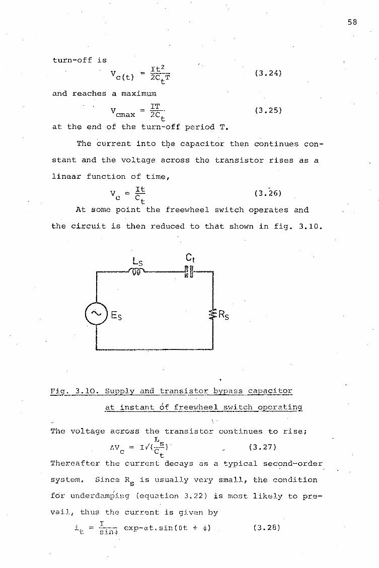
At some point the freewheel switch operates and
the circuit is then reduced to that shown in fig. 3.10.
Ls
Es Rs
Fig_:__]. lo~_ Supply and transistor bypass caoaci tor
at instant 6£ freewheel switch s>per.3..tins.
\ .
The voltage across the transistor continues to rise; r....
tN = r/{-cs} c t
(3.27)
Thereafter the current decays as a typical sec?nd-order
system. Since Rs is usually very small, the condition I
for underdamping (equation 3.22) is most likely to pre-
vai.l, thus the current is giw.~n by
exp-at.sin{Bt + ¢) (3.28)
58

where
and tan qi = .1.. 3IR ' s ~
It is obviously undesirable to turn on the power
transistor while the bypass capacitor is fully charged
since there ~s nothing to limit the rise of qurrent.
This problem is overcome by including a small value
resistor in series with the capacitor with a fast diode
in parallel. During turn-off the diode effectively
removes the resistor from the circuit, but brings it
into operation during turn-on.
turn-on is then Ve
1max = Rt + IL
Maximum current at
(3.29}
'!'he maximum voltage Ve is that of the supply;
that is, E smax'
Instead of the capacitor in parallel with power
transistor, it is possible to replace it with a zener
diode acting as an energy dissipater. Fig• 3.11
ZENER DIODE #'/7
~ ·--·-··--
Fi_g. 3. 11. Zener diode snubber
59

illustrates the arrangemente When the transistor is
turned off the current i.s diverted i'.nto the stray
capacity; the vol~age rise is very fast; , the zener
diode breaks over and conducts. The voltage across
the transistor is then held constant until the free-
wheel path comes into operation.
The advantage of the zener diode over the
capacitor as a bypass element is that excessive
collector-emitter voltages are avoided if the feed-. back system should by any chance be delayed in its
operation. Equation 3.27 indicateq that the voltage
across the capacitor rises as a linear function of
time, which could rapidly reach an excessive levele
The zener voltage remains constant and the only require-
ment is that the diode b~ capable of dissipating the
excess energy.
The disadvantage of the zener diode system is that,
since the voltage is constant, the danger of second
breakdown is enhanced. Fig. 3.12 illustrates the
turn-off loci of the two systems. The capacitor bypass
has a turn-off locus which can keep well clear of the
safe operating limits regardless of switching speed,
while the zener diode system pushes to the limits of
safe operation.
60

Zener
~ig. 3.12. Zener diode vs. R-C turn-off loci
I
Supply
o---v...AJ-..r--¥l•r----~
Ls Rs lRsup
c~~~~~~~~~~~-~-Csup·~~-0 Load
f'ig:. 3 .13.:......Bypassing the supplx
Excessive voltage excursions may occur in the final
stage~ of the switch-off process if the supply inductance
is overly large. This may occur when the system is
operated from a variable transformer, say fqr experi-
mental purposes. If the supply :i.s bypassed by a series
resistance-capacitance network, as in figc 3.13, and the
values are arranged such that
_where R = Rs + RSUP
R2
4L2 s
1 >--- (3.30) I. c s sup
then the system is overdarnped and no voltage excursions
can occur.
61

3e6 FEEDBACK CIRCUIT BEHAVIOUR: (24)
The voltage across the load comprises a forced component,
(3.31)
and a natural component during the transient period,
VLnat = -Ve (3.32)
Ve is the voltage appearing across the bypass capacitor.
If one considers the voltage appearing across the
freewheel transistor, then the diode bridge ensures a
uniform polarity irrespective of the behaviour of the
voltage across the load. Thus the requirement of the
feedback network is to discriminate between the
transient voltage, appearing at commutation, and the
"off" condition collector-emitter voltage VCE. The
maximum collector-emitter voltage is the peak value of
the supply voltage. ( In the "off" state ) •
Noting that the rate of rise of the transient
voltage is several orders magnitude larger than that of
the supply, two possibilities present themselves. These
are
* Absolute value detection by comparing the
transient voltage to a preset value which
is higher than the peak supply voltage • . * Rate of rise measurement by me~ns of a
differentiator circuit, and again com-
paring this to some preset value.
These possibilities are illustrated in figs. 3.14(a)
and (b) •
Further feedback circuit operation security is pro-
vided by the overall system control which inhibits
62
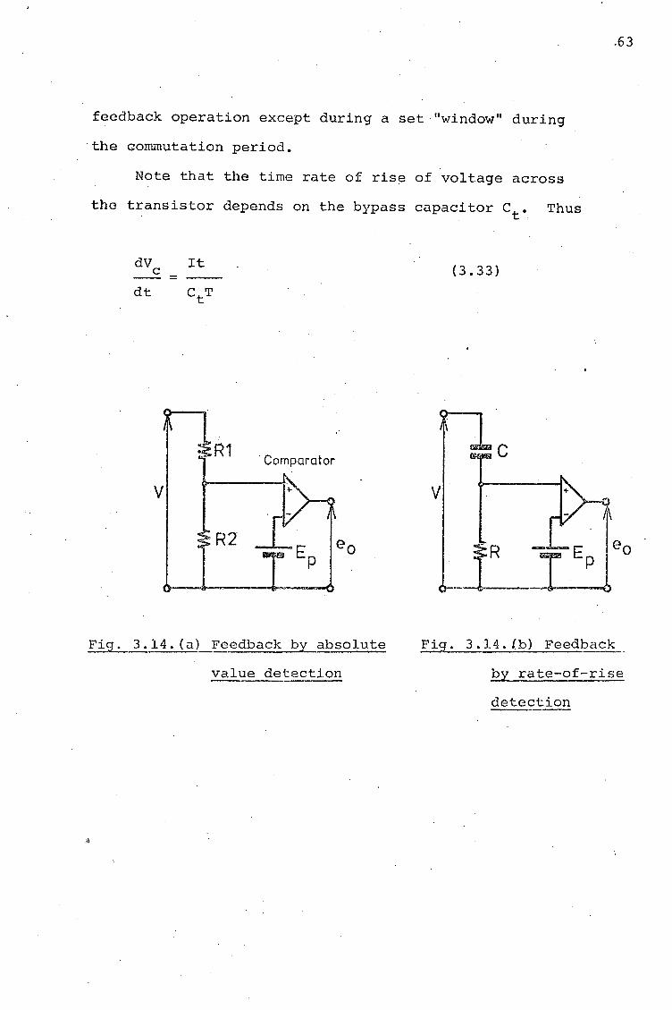
feedback operation except during a set· 11 window 11 during
the Gonunutation period.
Note that the time rate of rise of volt.age across
the transistor depends on the bypass capacitor Ct. Thus
dV c
v
= It
R1
R2
(3.33)
·Comparator c
v
.63
Fig. 3.14. (a) Feedback by absolute Fig. 3.14.{b) Feedback
value detection by rate-of-rise
detection
\\

CHJl.PTER 4
EXPERIMEN'I'AL REALISA'rION OF THE A-M.OD CONVERTER
4.1 INTRODUCTION:
The practical r~alisation of the converter system out
lined in the previous chapters involves two basic
elements. These are the power switch and the control
circuite A prototype of the complete system has been
constructed with a 6-pulse bridge configuration. Any
examination of the 3-pulse mid-point configuration
may be obtained by simply using one half of the
6-pulse bridge circuit.
Fig. 4.1 gives a block diagram of the system, for
a 3-phase input and single phase bridge output. Since
this represents the basic minimum converter the
description that follows centres on this system.
Three-phase output systems involve the interconnection
of a number of single-·phase systems.
The block entitled 11 switch'1 comprises the power
transistor, the diode bridge (to provide bidirectional
conduction), the base drive circuit, coupling isolators
and a power supply. The "control pulse generator" con
tains all the logic circuits to operate the switches in
the correct sequence at variable frequency, vary the
series/shunt conduction ratio and control the feedback
circuits.
The protection system provides a means of limi tin~;
the current and voltage applied to the power transistors.
Since the transistor has no reserve of short-term
64

64(a)
NOTE :
The shunt switch performs the function of
maintaining load current continuity during the supply
"off" period • That is , when one of the series switches
is opened , the shunt switch operates , under control
of the feedback system , to keep the (inductive ) load
current constant • When it is neccessary to recouple
the load to the supply , the shunt switch opens and the
feedback system operates the appropiate series switch •

·Over-voltage protection
Over-current protection
\ 0----...1
Supply phase 1
Series Switch
1----&---1
Control} pulse/ input
J, -~eedback y_---- enable
To other
Series I EJ o - .._ ___ ....... t---...... --s Swi tc'U~ I ~- Load -..i--~
Supply half phase 2 of
bridge
-Supply phase 3
Set Speed
~-~_..
Set voltage
Series 1--~~-~~ Switch
Control pulse generator
11 ~ / ~
Control Feedback pulse enable input
·~ Shunt control pulse
Shunt feedback enable
65

overload current capacity, and similarly has no self
protect capability on overvoltage, external means are
provided to protect the device. These comprise a
fast-operating "crowbar" fuse for current limiting,
and high-power surge suppressors for voltage pro
tection. The "crowbar" circuit is detailed in
Appendix 8.
4.2 DESIGN OF THE COMPLETE TRANSISTOR SWITCH:
The circuit associated with the power transistor
must meet the following objectives:
* Provide sufficient base current to turn the
transistor on, with a fast enough rise time
to avoid extending the 3 jJ sec delay in
herent in the power transistor at turn-,on.
* Prevent the power transistor from going in-t:.o
saturation.
* Provide a reverse-bias on the base of the
power transistor during the noff" period.
* The circuit must be able to operate while
floating at supply live-to-neutral
potential, i.e. some isolated interface
must be provided to the control pulse
generator.
* Provide a circuit for the feedback system
to operate over.
The complete switch circuit is shown in fig. 4.2,
and a detailed component function description is given
in Appendix 8, since it is only proposed to outline
here the salient features which give effect to the
66

r--.
IQ
Co
ntr
ol
inp
ut
27
0K
R
7
Fig
. 4
.2.
com
ple
te
po
wer
! 1120
R3
L ~55
v.1 T2
l R1
8012
4 -
Cin
·uF
--
?--
-
08
0
~-~-[>
! r
--tJ
. Pr
i I
N-.
J.73
1 .
i
V!~g""
~d--~.
0.1
I .
~,T1
I
02
IR
12
I
I ,,-----=~-! 2
0f j
,. I
07
I D1
1 I
012
l MA
IN S
WIT
CH
TER
MIN
ALS
l

requirements listed above.
The protection or "snubber" circuit for the power
transistor is provided by C3, Rl2 and D6. The values
sele~ted result in the feedback circuit, which depends
on time rate of rise of voltage across the power
transistor, being operative for load currents greater
than 0,3 A. The voltage rise produced by currents
below 0,3 A is negligible. Maximum voltage is limited
to 300 V by the protection diode which dissipates
30 m Joule on each turn-off operation.
Base drive to power transistor Tl is provided by I
transistor T2 which is connected in an emitter-follower
configuration. The switching times of T2, a type BD124,
are an order of magnitude faster than Tl, a BUY69B.
The diodes Dl and D2 are a Baker clamp anti-saturation
circuit which ensure that the base-collector voltage
can never be less than the base-emitter voltage.
The reverse bias to the base is provided by means
of Rl and diodes D3, D4 and DS, which make a 2,1 volt
positive bias to the emitter which is in effect a
reverse bias on the base.
Opto-couplers OCl and OC2 isolate the switch
circuit from the system control logic. The main con-
trol is through OCl while OC2 controls the feedback
circuit. Both of these devices are of the photo-
transistor-light emitting diode type, which are much
slower than the photodiode type. However, the output
of the phototransistor optocoupler is much greater,
and thus'the loss of speed was felt to be more than
offset by the simplifica'tion of the subsequent circuit.
68

Typical rise (and fall) times are 2 µsec, which when
added to the 3 µs~c delay of the power transistor,
makes an overall system turn-on delay of 5 µsecs,
mentioned earlier. Full specifications of this device
are in Appendix 5 •
The feedback circuit, which in this instance is
of the typ.e which detects the rate of rise of voltage
across the switch, is made up of capacitor C2 and
resistor Rll, operating into transistor TS. Transistor
T4 inhibits feedback action when it is not required.
Bidirectional conduction is provided by diodes D7,
08, D9 and 010. These are 600 V 12 A (av.) devices
with a 200 nsec turn-off, thus having a marginal effect
on the overall performance of the switch. Heatsinking·
is provided by means of 50 mm of the same extrusion
used for the power transistor and designed by the same
approach.
4.3 THE CONTROL PULSE GENERATOR:
The control pulse generator is required to fulfill the
following functions:
* Operate the transistor switches in an
ordered sequence as in fig. 2.3.
* Ensure that the feedback circuit comes
into operation at the correct point in
the operating cycle.
*Provide a means, if necessary, to.mak~
closed loop ~peed control of the load
motor possible.
* Vary the duration of the control pulses in
69

(
order to provide voltage variation, as
set out in section 2.1.
A functional block diagram, using positive
AND-OR logic, is shown in fig. 4.3. Power switches
for only one phase are shown.
The implementation of this simple sequence, shown
in fig. 4.3, requires that a voltage-controlled
oscillator (V.c.o.) drives a 6-stage ring counter,
with outputs gated to provide 120° phase displaced
signals. The output of the v.c.o. also drives the
pulse width controller which varies the control ratio
(section 2.2.l) under the control of an external
voltage. Design details of these units are to be
found in Appendix 8, while all the relevant waveforms
are shown in fig. 4.4.
The feedback ena.ble circuits, which comprise a
composfte unit for both shunt and series control, are
· critical to the operation of the switching system, and
are unique to it. Accordingly a more detailed
examination is presented here. Fig. 4.5 shows the
waveforms produced by this unit in relation to the
V.C.Oo, and fig. 4.6 gives a complete circuit diagram.
The truth table for the feedback enable circuits
is as follows:
I
70

~
..-l
i-
Fig
. 4
.3.
Blo
ck
d
iag
ram
o
f co
ntr
ol
pu
lse g
en
era
tor
Ga
ted
Rin
g C
ou
nte
r
J~et
ts
d
v.c.o.
1
2 3
4 ·5
6
pe
e
_ I
I I
-
Se
rie
s F
ee
db
ack
En
ab
le
.set
"'
--1
~
1·v
ott
s
I -.--
Pu
lse
S
witc
h C
on
tro
l
Wid
th
Sh~ F
ee
db
ack
Ena
ble
Co
ntr
ol
iA Sw
itch
Co
ntr
ol
LY
[Y
[r
I\
u D- ~· - .,._
~ -- ..
.- 1r-
-i
l i
I I
Se
rie
s
Sw
itch
es
Shu
nt·
Sw
itch

1
0 .1
0 1
0 1
_LL I -·---- I
~ ,
0 1
0
1
0 1 -·--
0
I I 1 · I I l CV
~
@ ..
l © -.
_J l @
__J ®l
~µ-u -lJLJlJ L _____ ----·
-7i !<_:-.Depends on voltage setting
Time ---Fig. 4. 4. Contr?l P.U1~~ generato5 wavef~
-
72
vco
Gated Ring. Counter Outputs
Pulse Vv'idth Contol

1
0
1
0
1
0
1 0
1
0
1
0
I -' I I I I
--I I I \_..
-, I I I I I I I I I I I I
I I I I I I I I I I' I 1' I I 1 I 11 I l 1
.___I (I l I I 1 11 I 1 -I , ,
I
I .-
vco - -=-
I I I I _J:-Puls
.... _ cont e width roller
I I I I I I I
~ I I I d '
es back ON
I I I I I . I I I I I I I
I I -I I Seri I I
es ON I
I I 'I I I I I i
h_ I I I I I Shun I I I ! feed I
t back ON
I I I I I I I I I I I I I In I I I I I ! Shu I I ,1 I I ,I
nt ON I 11 I 11
Fig. 4.5. Feedback enable waveforms
73

-l
I' ·~nit
Gate
d
Pu
lse
, S
eri
es
l Sh
un
t S
hu
nt
I Seri
es
Seri
es
Sh
un
t R
ing
w
idth
,
swit
ch
j f
eed
back
, sw
itch
fe
ed
back
sw
itch
sw
itch
. '
rime
l Co
un
ter
co
ntr
oll
er.
co
ntr
ol ! en
ab
le
co
ntr
ol
en
ab
le
! ,
I l
t 1
l l
0 0
0.
1 '
1'
0 .
I 0
l I
r-
i -
I -
l__2
_J
1 i
I i
o o
_
· o
i o
I t2
1
0 I
0 1
0 0
0 1
i
r-t3--~ I
0 0
ol I
l 0
0 1
I !
l •
I .
1-.
t :
Sta
rt o
f se
qu
en
ce;
·seri
es
feed
back
o
pera
tes
0
t1
: E
nd
of
seri
es
feed
back
p
eri
od
; seri
es
swit
ch
co
ntr
ol
op
era
tes
t2
: . S
eri
es
swit
ch
o
ff;
shu
nt
feed
back
o
n
(Vo
ltag
e co
ntr
ol
mo
de)
t3
: S
hu
nt
feed
back
o
ff;
shu
nt
swit
ch
co
ntr
ol
on
.
The
ab
ov
e p
rocess
is
re
peate
d,
t0
thro
ug
h to
t
3,
whe
n 6
-pu
lse b
rid
ge o
pera
tio
n is
re
qu
ired
.
-..]
.;:
..

Referring to fig. 4.6, positive-going pulses from
the pulse width controller trigger monostable multi-
vibrator MSl. The Q output of MSl is applied to 2-input
NAND gate Nl together with the Q output of MS2. The
output of Nl then goes low, and this activates the
series switch feedback circuits through inverter-
drivers Dl to D6. The high pulse from the PWC is also
applied to the D input of bistable DFl, and, through
inverter I, to the D input of DF2. DFl remains un-
changed as the clock input is still low, while the
Q output of DF2 goes high, which switches off the
shunt switch through inverter-driver D8 • Monostable
MSl remains high for a period of· 50 µsec maximum,
which is the commutation period. When MSl goes low, '
the Q output triggers MS2 which extends the duration of
the feed.back circuit operation for a further 10 µsec
maximum, in order to o.llow for the turn-on delay in the
power switch. The bistable DFl clock input goes high
when MSl goes low, through NAND gate N2, and the hig·h
pulse from the PWC is then entered into DFl which
enables the gated ring counter outputs to operate the
appropriate series switch. The Q output of MS2 is also
applied to NP.ND gate N4, preventing any operation of
the shunt switch during this period.
When the PWC signal goes low, monostable MS2 is
triggered, the D input of DFl is removed and a high is
applied to the D input of DF2. A similar process to
that described previously is then followed, with MS4
providing the additional pulse to compensate for turn-
on delay.
75

PWC'
MS1 ---0
----'Q
I
MS2
---a
MS4
N1
DF1
Series Feedback Enable
--0:,ies Switch. Control
Shunt Feedback
N3 Enable Q----{r
Switch Control
fig. 4.6. Feedback enable unit circuit diagram ----
76

The sum of the cormnutation and turn-on times means
that there is always a gap between steps of the series
switches. That is, if one refers to fig. 2.1, the
wiper of the switch goes into a dead time between con-
tacts. The monostable multivibrators MSl and MS3 were
I set to a pulse duration of 25 psecs and MS2 and MS4
were set to 5 µsecs, which gave a total duration of
30 µsecs. Since the changeover from one series switch
to another involves turning off the first switch, with
attendant 30 µsecs delay, and then turning on the next,
which also produces a 30 µsecs delay, the total gap
between switches is then 60 l1Secs. This imposes a
maximum limit to the on-off ratio, i.e. a "full-on"
condition cannot be achieved. The maximum on-off ratio
at 50 Hz output, was set at 4,5 : 1.
The frequency range of the voltage-controlled
oscillator is in fact wide enough to investigate the
pos-sibilities ·of "slow" sampling or sampling at a rate
(w. - w ) • J. 0
(See Appendix 1.)
77

CHAPTER 5
RESULTS OBTAINED FROM THE EXPERIMENTAL MODEL
5.1 Test methods and equiE.ment;,:
Test results were obtained using standard laboratory
test instruments, as indicated in Fig. 5.1, which shows a
typical configuration for measuring the output waveform,
both for waveshape and spectral content. Current wave
forms were evaluated using Hall-effect transducers to pro
vide isolation.
5o2 Test results; waveforms:
Figures 5.2 to 5.13 illustrate typical waveforms ob
tained from the transient recorder. ConLTUent follows in
numerical sequence:
Fig. 5.2: Output waveform from a 3-pulse system with
v.c.o. set at 600 Hz and pulse width variede
The zero line is added in.
Fig. 5.3: Output waveform from a 3-pulse system with
v.c.o. at 480 Hz and pulse width varied.
Fig. 5.4: Output waveform from a 3-pulse system with
v.c.o. at 360 Hz and pulse width varied.
These three figures illustrate the fabrication of the
output voltage waveform from the 3 supply phases and how
the mean output voltage is varied by pulse width control.
F~g. 5.5: Figs. 5.5(a) and 5~5(b) show, on an expanded
scale, the output voltage with the v.c.o. at
600 Hz and 480 Hz respectively and pulse width
ratio of 0,8. The voltage spikes required by
78

NEUTRAL
Fig. 5.1.
'
From other supply phases
.,g_;;___,i.-------iswitch.
Svvitch
X-Y Recorder
_ _,. __ Spectrum Analyzer
Transient
Recorder
[=r_:; X-Y ·. __ J Recorder
LOAD &---~;,;. J
~ To neutral or hait-bridge
Testing the system. The anuneter and wat.tmeter
elements were replaced with Hall-effect
transducers in order to obtai~ permanent
records via the transient recorder - X-Y -··------------record.er •
79

(d)
80
10QV
-100V
'JOOV
-'100V
··-- -· -·~--··"' ····- -··--,.- -~~···-·-·· ..... -·- ---~- ......... ·--,.~--·---- . --
100V
-100V
100V
-100V
0 .___--~--~--+-·~·~~~-----+
20 40 TIME fmSe~J_
Fi S. 5 • 2 ,, Ou S?..~-~<l.V.~ (QEEJ._..;_J_0
:= 5 O Hz • i.?-LL....:s= O LL Jc U r== O ci ~(l?J .~ r"'"'o~(d.)_.:__r=C2,d

81
100V
(a) o
-100V
100V
{b) 0 .
-100V
100V
(c) o
-100V
100V
(d} 0
-100V
.__~--"~-~-··~-I--~~~~ 0 20 40 60
TIME[mSec]
Fig. 5~3. Output waveform i f = 30 Hz • (a) : r=0,8 , (b) :r=0,6 -- ·-----· 0 ---------- ____ .
( c) : r::~o / 4 , ( d) : r=O, 2

' .
l . . I ~\I ;~"i • · I . ! Ii J . I
-100V \ ' ·•
-· ,.l
-100V --
~~--4-~---~~-1-~-· 0 50 100 . 200
TIME[mSec}
Fig. 5.4. Output waveform ; f = 10 Hz • (a) :r=0,8 (b} :r=0,6 0
( c) : r=O , 4 ( d) ; r=O, 2 ..,, ---
82

.... , ~- -- __ ...... _,__ ___ ,~-·-.-..-~..->·,.---·""- .... _ .... __ ............ _. ___ --- .. ...,__, ___ ....... ....;. .... ~ ·---·-·- .. ,.~__,'""-~·-~- .... ....___
100V
(a) o
-100V
100V
(b) 0
-100V .. vi (c) SA -·t-. ---"-----'"'--_._--___.1,~---·1 _____ ,__,_L-
0 100\/
(d) 0
-100V
-.._,--------:.-------=~1-·~---·=·-www•~~ 0 10 20 30
TIME[mSec]
Fig. Sos. Output waveform ; (a): Voltage , expanded time sc.ale--,-~f = 56Hz , r::=O, 8
0
(b) : Voltage , expanded time
scale 1 f =30Hz , r=0,8 . __ o ___ . --------
( c) : Load current , inductive load. ___ _
(d) : Output voltage , inductive ----·r0aa···-----------·-----··--···-·-
83

the feedback commutation system appear clearly
at turn-off points. Figs. 5.5(c) and (d) show
load current and output voltage respectively
84
for a 3-pulse system into an inductive ( i = 0,014 )
load and here the output voltage waveform
illustrates the commutation problem mentioned
in para. 3.4, where the load possesses a
nback-e.m.f.".
Fig. 5.6: Figs. 5.6(a), 5.6.(b) and 5.6(c) show output
voltage, current at the junction of the 3
switches and load current, respectively, for a
3-pulse system operating into an inductive lc,::i.d
and illustrate the correctness of the assumption
that the load currertt is sinusoidal.
Fig. 5.7: Figs. 5.7(a) and 5.7(b) show, respectively, out
put voltage and input power, the latter obtained
by means of a Hall-effect transducer in one input
supply phase. The v.c.o. was set at 600 Hz, that
is, an output frequency of 50 Hz, which enabled
a transformer supplying a 50 Hz signal to be con
nected in series with the load. This results in
an output as in Fig. 5.7(c) and an input power in
one supply phase as per Fig. 5.7(d). The re
generation capability of the system is clearly
illustrated here.
Fig. 5.8: The output voltage was separated into positive
and negative banks by means of diodes in the
supply phases, to produce the ·waveforms of
Fig. 5.8(b) and (c), while Fig. 5.S(a) shows
the total output. This is to illustrate the
avoidance of the bank selection.problem which

100V
(a) o-
-1oov ~
SA
(b) 0
-5A
5A
(c) 0
.., 5A
0 50 100 TIME [mSe_c]
150
Fig. 5.6. (a) Output voltage , inductive load
(b) Switch current , " II
------(c) Load current , 11. II ,
--------
85
/

- 86
- - -
100V
~4i r~ ~~~1~ ~ ~ (a) 0 ~f ~\~M ~] . :~P . u~
-100V ..
~ -•.- . --- . - ·- - ··- - --- -- . --- .. --- ... - -
50W
(b) 0
(d) . 0
-50\V
~-----+-1 ----·-----,---+·-~--0 20 40
TIME[mSec]
Fig. 5.7. Power in ~he system - . --
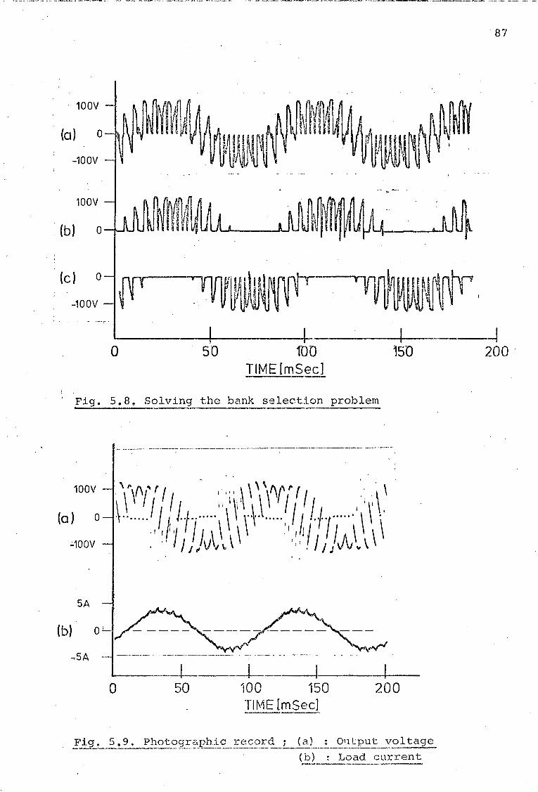
· 100V
(a} o
-100V
100V
(b) 0
· n ~,~/Ml __ ........ ~1~ 1 urw
-- ""' ---
87
lc~1oov0
~~V~~~JW, I
0 50 100 150 TIME [mSec]
Fig. 5.Bs Solving the bank selection problem
-- ----- ~--~----·---·-··-· ----·---··----··--- --------·--· ________ ..., __ ------~-... --- -··---·--
.:..1oov
(b) 5A QL/-~-----~ -~~ ---"~
-.5A - ------ - ----~--·--·-·----· · --- --·----- - - --- --- - - - · ·
j 0 50 100 150 200
TIME [mSec]
Fig. 5.9. Photographic record ; (a_) : 011t:put voltage ------·-----·-·-----------··•··--~·-u----·-··---·-•~-~--·-•-••,_._ _____ _......,._~-----
(b) ~ Load current
-~ 200.
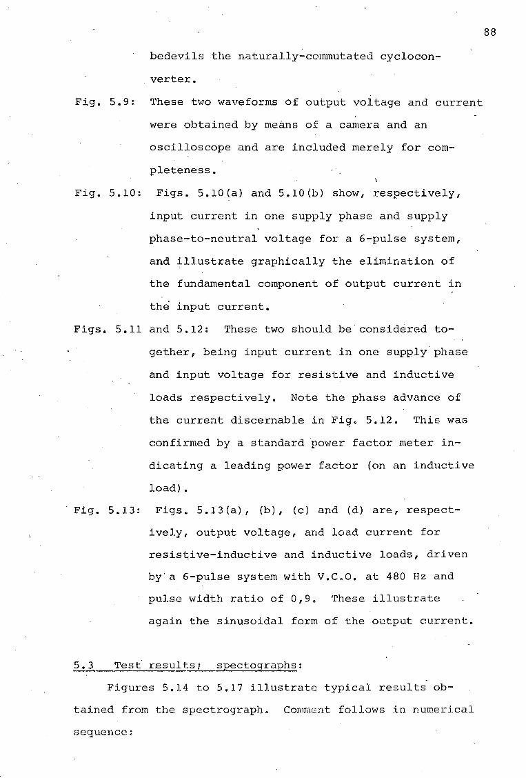
bedevils the naturally-commutated cyclocon
verter.
Fig. 5.9: These two waveforms of output voltage and current
were obtained by means of a camera and an
oscilloscope and are included merely for com
pleteness.
Fig. 5.10: Figs. 5.lO(a) and 5.lO(b) show, respectively,
input current in one supply phase and supply
phase-to-neutral voltage for a 6-pulse system,
and illustrate graphically the elimination of
the fundamental component of output current in
the input current.
Figs. 5.11 and 5.12: These two should be considered to
gether, being input current in one supply phase
and input voltage for resistive and inductive
loads respectively. Note the phase advance of
the current discernable in Fig. 5612. This was
confirmed by a standard pov.,rer factor meter in
dicating a leading power factor (on an inductive
load).
Fig. 5.13: Figs. 5.13(a), (b), (c) and (d) are, respect
ively, output voltage, and load current for
resistive-inductive and inductive loads, driven
by· a 6-pulse system with v.c.o. at 480 Hz and
pulse width ratio of 0,9. These illustrate
again the sinusoidal form of the output current~
5. 3 Test results L _s12ectographs:
Figures 5.14 to 5.17 illustrate typical results ob
tained from the spectrograph. Comment follows in numerical
sequence:
88

;
I . I
SA
(a) 0 rJ~ -5A i . ~
100V
(b) 0-
\ -100V
I
~~--~1--~--rl~~~~·--~.-1 -----~-0 40 80 120 140 160
Fig. 5.10. 6-Pulse system ; (a) Input current
(b) Load current
89

5A
(a) o
-5A
50V
(b) 0
-50V
0
_, ________ _ 20
TIME[mSec]
Fi_g. 5.11. Resistive load ; (a) In_put currt:.!1t.
(b) Supply voltage .
90
-- I --40

5A
--5A
50V
(b) 0
-50V
0 20 TIMEfmSec]
Fig. 5.12. Inductive load ; (a) Input current
(b) Supply voltage
91

92
. . -.
N v A l I Vi j I I 'u i , .
-100 '
. - ·- .. - ·-- - -·-··- - -·· -· - ---·~ -- --·~ -~ -------- ~ . .., ··---- .. ·- . .
5A
0
··5A
100V
0
WI -100V
---
~ 5A
0
-5A
'------ - ~i--------+---0 0 80
Tl!~~ f rnSec]
Fig. 5.13e 6-Pulse system ; £0
== 30 ; r = 0,9 ------------·--·---------

Fig. 5.14: Spectra of output voltage of 3-pulse system
for v.c.o. frequency of 600 Hz and voltage con-
trol ratio of 0,8 for Fig. 5.14(a); voltage
control ratio of 0,2 for Fig. 5.14(b). Note
that, unlike the naturally-commutated cyclocon-
verter, the frequency of the harmonics does not
change with output voltage.
Fig. 5.15: Spectra of output voltage of 6-pulse system.
The v.c.o. frequency for Fig. 5.lS(a) and
Fig. 5.lS{b) is 600 Hz and 360 Hz for Figs.
5.15(c) and 5.15(d). The voltage control ratios
are 0,8 for Fig. 5 .• 15(a) and Fig. 5.15(c), and
0 , 2 for Figs • 5 • 1 5 ( b ) and ( d) •
Fig. 5.16: Spectra of input current per phase with single \
phase output, inductive load, with voltage con-
trol ratio of 0,8 for Fig. 5.16(a) and 0,2 for
Fig, 5.16(b). Note the preponderance of
harmonics at low voltage control ratios.
Fig. 5.17: Spectra of input current, v.c.o. frequency
600 Hz and voltage control ratios of 0,8 and
0,2 for Figs. 5.17(a) and 5.17(b) respectively,
with resistive load. This represents an un-
usual case of non-sinusoidal output current,
but is included to show the generation of
harmonic pairs as predicted in Chapter 2.
Figure 5.18 shows the relative amplitude of the
harmonics present in the output of a 6-pulse system driving
an inductive load; this should be compared with Fig. 2.7(b)
93
which gives results calculated from the analytical expression

100V
50V~
{a)
(b)
0 _J
50V
0
0
Fig. 5o14 ~ out.put v-~~lt_a~~ sp~ctru~~-p~I~e sys~_em
f ::::: 50 Hz , (a) r= o,8 , (b) r=~ o,2 0
94

5QV
(a)
0
5V
(b) 0
50V
{c)
0
5V (d)
0
Fig. 5.15$ output voltage spectra,
6-pulse system
{a) : £0
= 600 Hz
r =-= o, 8
{b) : .
95
_ _JJ_.jj..____LL_ f = 600 Hz 0
r = 0,8
0
(c) f = 360 Hz 0
r = o,2
l __ _J_ ___ ~-h~~"--~-
_l_LJ_ _ _J_ __ L__ (:: ~ 360 Hz
------+I r = o, 2
2

96
-
-
(a)
I 0 I-
ll . _J_ - - -
0,5A -·
{b)
n i
.._ .._____ .___ L 0
I -. 0 1
Frequency (kHz)
Fig. 5.16. Input current spectra , single phase inductive
load f = 50 Hz , (a) r= o,8 (b) r= 0,2 0 ---------.. ------·-

97
1A
(a)
0
0,5A
(b)
0
0 2 . Frequency (kHz)
Fig. 5.11. Input current spectra , single phase resistive --~ ------
load , f = 50 Hz , (a) r~ 0,8 (b) r= 0,2 ____ o. ___ _

98
1,0
0 0,1 0,2 0,3 0,4 0,5 0,6 0,7 0,8 0,9 1,0 Control Ratio [r]
Fig. 5.18 Relative harmonic amplitudes , 6-pulse system

'-0
,7
u ,4 {1_ c 0
+:: L-o -(/) ' b -c Cb L. L. :J u
,1
0 0' 1 0, 2 0, 3. 0,4 0. 5 0, 6 0, 7 0, 8 0,9 1, 0 Control Ratio [r]
Fig. -s~l9. Input current.distortion factor
99

,9
,8
,7
,6
Vin ,5
Vout.4
,3
' 1
\ .
0 OJ Q2 Q3 Q4 Q5 Q6 Q7 QB Q9 tO Control Ratio [r 1
Fig. s.20. Voltage control action
.. , ..
100

101
1,0
0,8
0,6
0,2
0 0,2 0,4 0,6 0,8 1,0 Control Ratio[r]
Fig. s.21. Input power factor , resistive load

100
80
;: Cf)
~ 60 Cf) 0 __.
J::. u ~ 40 ~
(/)
20
0 2 3 Av Current [A]
Fig. 5.22. Switch losses
102
5

. 103
for output voltage. Note that Fig. 5.18 does not indicate
the negative-going part of the curves since-the wave
analyser used to obtain these data is not phase-sensitive.
The input current ~istortion factor, shown in
F~g. 5.19 and obtained by means of a wave analyser ex-r •
amination of input current, should be compared with the . calculated values shown in Fig. 2.12.
The vo'ltage control capabilities of the converter are
shown in Fig. 5.20. The test result agrees well with the
result predicted in Chapter 2. Note that the output voltage
in this case is the effective value which includes harmonics.
This curve should be compared with Fig. 5. 18 (m = 0) · as an
indication of voltage control operation. ··
Switch losses as a function of current for one unit
with control ratio as parameter and unity power factor load
are shown in Fig. 5.22 while input power factor, for the
same load, as a function of control ratio is shown in
Fig. 5.21..
The results shown graphically in Figs. 5.20 to 5.22
were obtained from readings of standard moving iron volt-
meters and anuneters and electrodynamic wattmeters. Thus
there is bound to be some error as the response to the
complex ·waveforms produced by the converter is not known
accurately. However, there is a broad agreement which
gives. one confidence both in the test results and the
derived expressions.
Figs. 5.23 and 5.~4 are the waveforms obtained from
one switch driving an inductive load ~rom a D.C. source.
These illustrate normal commutation (Figo 5.23) and the
fault condition of simultaneous switch operation (Fig.
5.24). Referring to Figo 5.23, the shunt switch opens at

Ao The bypass capacitor, which in this case had a 1 ohm
resistor in series, charges from A to B. Note that the
current continues unchanged. At B the series switch is
fully operated and the current changeover.takes place.
~he ririging at C represents the discharge of the R-L-C
second order load circuit, as indicated in para. 3.5.2.20
. 104

·. 105
-.
ro Vol tag acros~ load ;..... -
........ I'-...
Q'J/ l/ --...... ~ @~ ~ 20 v
~-'
®" 2)1sec
Load current / \/ I
A ;
~ 2,5A
/ -Sunnlv current
Fig. 5.23. Switch conunutation , correct operation
Fig. 5.24. Switch conunutation , current·overlap
... ·sAj rrE TRJ' t'.ES A! FIG. b.23 ~ . .. .
• . . SAi llE SCJ\ ILES A~ FIG. D.23 ' ..... ... --- 'WI~ .
-'i·-
. . . . .. ... /' . . . . . -. . ..
I I -,
J \ . , , . I
~ \ ..
' ·~ . ,,
.

. 106
CHAPTER 6
A REVIEW AND SOME OBSERVATIONS:
6. 1 GENERAJ.J COJV"J.M.ENTS - THE ADVANTAGE OF THE SYSTEM
The system described in this work fulfills the require
ments expressed in Chapter 1 for controlling the speed of
an induction mot.or. That is, the a-mod converter enables a
fixed-voltage fixed-frequency supply to be converted to a
va.riable-frequency variable-voltage source.- This has been
accomplished using an electronic switch comprising a power
transistor, fast-switching diodes and associated drive
circuitry. This places a power-handling limitation on the
experimental model, but as higher-powered, transistors be·
come available this will vanish. The question may well
arise at this stage as to whether a force-crnnmutated
thyristor would not be more suitable, owing to its inherently
greater robustness. There are two major problems with this
approach.
The slowness of operation of even the fastest thyristor
would place a severe limitation on the higher frequencies of
operation of the system, when the output frequency approaches
50 HZ. It is possible to postulate that the system should
operate in what has been termed the "slow-stepping" mode (14)
but this introduces unacceptably low frequency supply current
harmonics. Naturally this speed lirni ta.tion would prevent
operation above 50 HZ - a limitation which appeared even with
the transistor switch employed.

107
The force-conunutati.on would require an external energy
source, as the periodic nature· of the a.c. supply make a
self energised system a hazardous proposition. This then
would involve a considerable multiplication of the com
plexity of the system, and the commutation system would also
demand an additional time penalty as energy storage elements
require charging time.
The advantages of the system - that is, features ad
vantageous in themselves, and not in comparison to any
"competitors 11 may be stated as follows:
* Inherently fully regenerative without any power-flow
sensing elements needed for control.
* Harmonics not likely to produce excessive unwanted
torque components in the output of a machine coupled to the
converter, even at standstill. In the event, filtering
would be simple to arrange. (7)
* Reasonably low distortion factor in input current and
output voltage. Again, if filtering is required, the demands
placed on such a filter would not be excessive.
* The control circuitry is not complicated to the point
where reliability would be impaired, being comparable to
most variable-speed drive systems. (13) It would, however,
be wrong to assume increased simplicity as a particular
virtue. (14)
* The output frequency is unlimited, with the only re
striction being the operating- speed of the switching elements.
In particular, the control is 11 smooth" around zero frequency
output arid may reverse the direction of rotation of an in
duction motor without any need for reconnecting any windings.
This may well be an advantage in the ''inching 11 operations.
The work of Schauder (ref. 7) · in th.is regard provides

108
ample confirmation of the virtues of the a-mod converter as
a supply to a variable-speed induction motor.This has been
confirmed by a limited test (speed-torque ) on a 4-pole 50 volt
6. 2 LIMITATIONS OF THE SYSTEM : machine •
The use of current state-of-the-art high voltage power
transistors has still shown a serious limitation to the
maximum power available from the converter. Even with the
BUY69A transistor it is still not feasible to operate a
380 volt machine from the experimental model. Higher
voltage transistors, usually developed for T.V. work, are
of a lower current rating and would have to be paralleled to
supply a sufficient current to make possible reliable operation
of even a 5 kW motor. (It is considered here that a large
field of application lies open for drives in this class.)
When transistors with higher ratings become available
then the situation will change except for the problem of
base drive current. While it is possible to supply any base
current demanded, the problem of providing this economically
is a large one. The Darlington configuration transistor (or
a Darlington circuit built up of individual transistors) _is
a likelihood but this usually drives the driver stage into
saturation and leaves a higher voltage drop across the power
transistor.
Hcwever, it should not be considered that the power
transistor inherently represents a block to any further de
velopment.
The opto-coupler used is a compromise between gain and
speed. An earlier experimental model was attempted using
diode couplers. The high transfer loss of the device placed
an undue emphasis on the subsequent stages and this approach
was abandoned when it became clear that the speed loss was

'
more than offset by the lower transfer losses of the trans
istor. coupler~ However, the relatively low current of the
experimental model meant that the snubber circuit was able
to allow £or the circuit delays. If a very much higher
crirrent ·1s allowed then the use of the snubber network for
this purpose might no longer be permissible and high-speed
opto-coupler, of low loss, would have to be found.
Protection of the power transistor does represent a
problem. 'rhe "crowbar" system adopted has the virtue of
effectiveness, but it would be much simpler to use fuse
protection on its own. Since this matter is a peripheral
detail it does not inhibit the overall system operation,
and, like larger transistors, will no doubt be solved as
faster fuses appear.
A_serious impediment to the use of power transistors
is, however, the apparent deterioration of these devices
when switching inductive loads. Gaur and Lowe have re
ported (23) that defects appeared in the structure of a
power transistor chip after some 1000 hours of on-off
switching, without any variation of electrical parameters
being apparent. This would no doubt lead to what have
been regarded as inexplicable failures in the past. No
indication was given in this paper of the ratings of the
device or of the voltage and current levels, except that
second breakdown was avoided. It could well be that a
generous rating system would mj.nimise this cause of failure.
A final limitation, inherent in the system, is the
power factor inversion phenomena. Strictly speaking, it
could be argued that if a load demands lagging volt-amperes
reactive, then the supply must supply a lagging p.f. and
nothing else. However, it should be borne in mind that in
109

the a-mod converter, a three-phase supply is switched to a
single-phase load, and thus a conventional power faqtor
meter would not necessarily reflect the true position. It
is khe power factor meter that gives the supply authority
his indication, and so the a-mod converter does represent
a problem. A simplistic approach to this occurr~nce is
not sufficient to explain the complex modulation process
which occurs, but until a different approach to power factor
prevails, any supply authority is bound to frown on a device
drawing leading volt-amperes, even if only apparently.
In sununing up, it may be said that the a-mod converter
has few inherent limitations, and most of the present
limitations are those imposed by current technology on the
switching device.
~~E FURTHER POSSIBILITIES:
As with the classical cycloconverter (9) it is possible
to modify the circuit configuration in order to obtain en
hancement (or suppression) of certain features of the a-mod
converter.
If a lower distortion factor is aimed at, then the
pulse number may be increased by using· a polyphase trans
former to increase the number of supply phases. The addi
tional cost of a transformer would have to be borne as a
penalty, as well as the increase in the number of power
switches and control circuitry.
A reduction in the amount of converter "hardware" may
be achieved by means of the "open-delta" connection. In
this system only two (single phase output) converters are
used to generate a three-phase output. This is possible,
since, for a balanced three-phase system of voltages, any
110

Fig. 6.1. The Open-delta connection
I I
N o---------_,.__;;i,_,_..!..1 _.__~ ~ : I~2
VOLTAGE PHASOR DIAGRAM
CURRENT PHASOR DIA.GRAM . .
I = I - I l pl _p2
0 = yl3I/30
I - I p3 pl
I I I I
Load
-----~"
J
111

112
one phasor can be generated from the summation of the other
two. Fig. 6.1 shows a schematic illustration of the arrange-
rnent. The disadvantage of this system is the inherently
lagging displacement factor of the system. A unity dis-
. 0 placement factor load appears as a 30 lagging load, as
shown on the current phasor diagram in Fig. 6.1. (Although
midpoint converters are shown in Fig. 6.1, obviously bridge
converters may also be used.) In addition to the displace-
ment factor.problem, care would have to be exercised in en-
suring proper synchronisation between converters. On balance,
the economic advantages of the open delta may well outweig·h
the disadvantages.
The freewheel switches of the bridge-connected converter
may be eliminated by a process known as "backstepping". That
is, when it is desired to turn off the supply current, both
ends of the load are connected to the same supply phase for
the duration of the freewheel period& The only penalty in-
curred is a slight increase in the complexity of the control
circuitry and also this only applies to the bridge connection.
Fig. 6.2 illustrates the operation. This system is decidedly
the approach to adopt in any commercial application.in the
lower power range where the cost of the electronic equipment
is a deciding factor.
The experimental converter described operated only in
the open-loop mode, but there is no limitation on using, say,
a tachometer feedback system to control the system. This
could also be coupled with c·t1rrent transformers in the supply
lines to exercise control over the current. These are
standard control· strategies for inverter-fed induction motors
and their application is covered in refs. (4), (13), (25) and
( 32) •

113
CUI~RENT ~JID'X?,3 ~- wmcaa
/. ~
.., -· ~ I I .
I I .,
'
~ /. -SUPPLY CONDUCTION
CURRENT
~-1 J---~~--------~>-------<>-~
FREEWHEEL CONDUCTION
f.ig.6.2. Bac~st~ping mode

The question of operation at higher voltages and
currents, with particular reference to the feedback system,
des~rves some further attention. It has been pointed out
that, in the experimental model, there is a finite delay
in· the operation of the feedback system. This is unavoid
able in any configuration, and the poss.ibili ty arises that
at high currents, say hundreds of amperes, the voltage rise
across the "turning-off" transistor might reach catastrophi
cally high levels. Assuming that turn-on delays do not in
crease, and there is no reason to believe that they should,
then a ten-fold increase in current produces (for constant
inductance) an equal voltage rise. An examination of
equations 3.27 and 3.28 shows that the voltage rise is also
114
a linear function of bypass (or snubber) capacity, and thus
one can easily postulate a considerable increase in the value
of this capacitor and still remain within the bounds of
reasonableness. Thus, the feedback system is well able to
function at considera.bly increased power levels, and must
play an important part in making the reliable operation of
the a-mod converter possible.
6.4 AN ECONOMIC COMPARISON WITH OTHER DRIVE SYSTEMS: -
The survey by Ludbrook (31) provides an excellent base
for discussion. Firstly, it should be noted that the non
regenerative d.c. drive remains the cheapest, but is not
necessarily the best for all applications.
Any comparison with the a-mod converter should be made
on equal terms. That is, any comparitive system should be
regenerative and able to operate a standard machine. Thus,
the comparison will be made with the following:
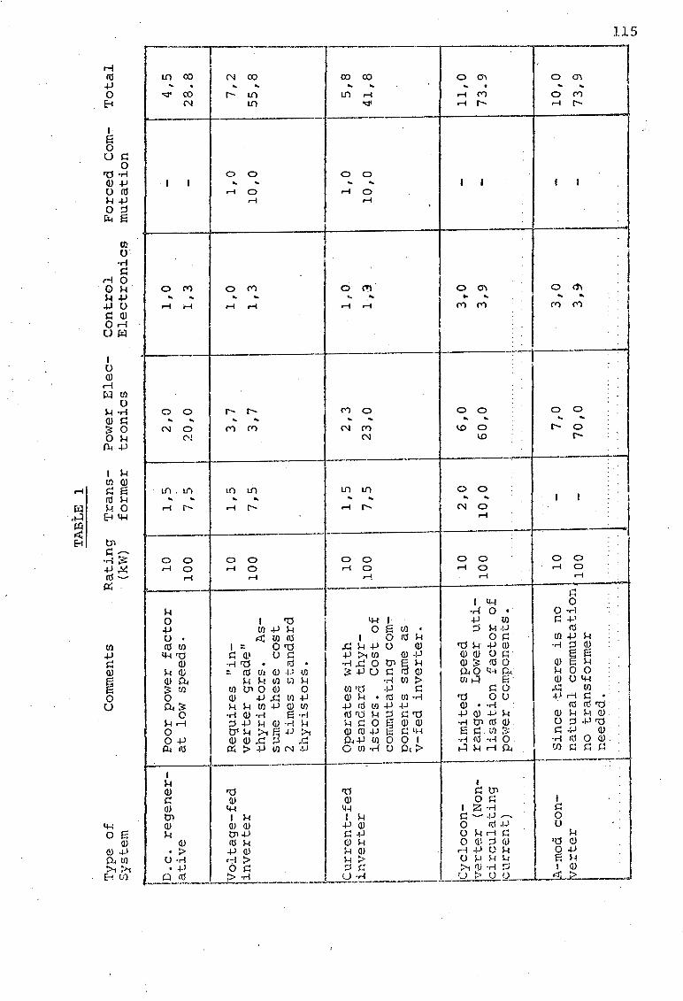
Typ
e o
f S
yst
em
Co
mm
ents
Po
or
po
wer
facto
r at
low
sp
eed
s.
TA
BL
E
1
Rati
ng
(k
W)
10
10
0
Tra
ns
form
er
1,5
7,5
Po
wer
Ele
c
tro
nic
s
2,0
20
,0
Co
ntr
ol
Ele
ctr
on
ics
1,0
1,3
Fo
rced
C
orn
mu t
at io
n
To
tal
4,5
28
.8
ID.?
. re
gen
er
jati v
e
' ~
--1
Req
uir
es
"in
v
ert
er
gra
de"
thy
ris
tors.
As-
Vo
ltag
e-f
ed
in
vert
er
1 su
rne
these
co
st
10
10
0
1,5
7,5
3,7
3,7
I 2,
t;:i
;ies
sta
nd
ard
I
I , i:n.y~~stors.
L I
j_
I
ku
rren
t-fe
d
\ Op
er~t
e~ w
ith
I l
0
II l,
5 2
, 3
. 1 1
inv
ert
er
I ~tano.ara
thy
r-I 1
00
7
5 2
3
o is
tors.
Co
st o
f ·
' 1
'
co
mm
uta
tin
g corn~
po
nen
ts
sam
e as·
v-f
ed
.i
nv
ert
er.
l
I-·
1,0
1,3
1,0
1,3
1,0
10
,0
1,0
10
,0
7,2
55
,8
5,8
41
,8
Cy
clo
co
n-
I Lim
ited
sp
eed
.
10
I
2,
0 l
6,
0 \
3, 0
I
-1
11
, 0
v2
.rte
r (N
on
-I
ran
ge.
Low
er u
.ti-
10
0
10
0
60
0
3 9
-7
3.9
circul~ting
I li
sat.
ion
fa
cto
r o
f 1
' '
'
~urr
em:)
I pow
er co
mp
on
en
ts.
·I I
I· . -~
· 1
~>.-mod
co
n-
I Sin
ce th
ere
is
n<
;> 1
0
1 1
-1
7 , 0
3
,0
3,9
10
,0
73
,9
rerte
r
ll n
atu
ral
com
rnu
tatJ
.On
1
00
-
I 70
0
no
tr
an
sfo
rmer
'
I-'
I . j
nee
d~d.
. .
. .
l· . ..
.......
f . .
.. . . ...
. ~
I ~-
----·
I-'
I.JI

* D.C. Regenerative drive {D.C. motor fed from
dual converter)
* Voltage-fed inverter to induction motor, re
generative
* Current-fed inverter to induction motor
* Cycloconverter
The following assumptions are made about costs:
*Cost of transformers proportional to 1,5 X
{rating) 017 • It is assumed desirable to
operate all-drives from a transformer intended
to supply commutation leakage reactance. The
a-mod converter does not need this transformer.
*cost of thyristors and transistors proportional
to rating.
*cost of electronic control circuitry, and aux
iliary controls such as interlocks, proportional
to {rating) 011 • This includes thyristor firing
circuits and transistor base drives.
*cycloconverter ar.d a-mod converter power devices
*
*
yield only half the power of d.c. bridges because
of duty cycle considerations.
Cost of a power diode is one third that of a
power transistor or thyristor.
Cost of commutating components proportional to
rating. {Inductors and capacitors.)
The relative costs are tabulated in Table 1. Although it
116
might be possible to dispute the basis for the cost comparison
on an absolute basis, thi.s table shows that the a-mod converter
is cost-comparable with the cycloconverter. In every case it
might be argued that the competing system ha.s a glaring defect
which makes it unsuitable for some or oth(~r application, e.g.
Drive System
D.c. regenerative drive
Voltage-fed inverter
Current-fed inverter
Cycloconverter
Defect
Uses d.c. motor with attendant commutator problem
Commutation problems
Uneven rotation at low speeds
Limited spe'ed range
117
'
Thus taken all around, the a-mod offers a premium performance
at a cost comparable to its competitors.
6.5 FINAL CONCLUSION:
This thesis has examined in detail a direct a.c. to a.c.
frequency converter. A member of the cycloconverter family,
it has been given the name of asynchronous modulation con-
verter to distinguish it from the other converters which need
to be synchronised to the supply frequency. Expressions have
been derived for the input current and output voltage and
these have been verified experimentally.
The experimental model, using power transistors as switches,
demanded that a ·feedback system be developed to make their
(the transistors') utilisation possible. The operation of
this feedback system has been examined and described j_n detail.
From the experimental model, desj_gn cri t.eria were established
for the system, making further development possible.
Plate l shows one of the switch units of the
experimental model . Clearly to be seen are the snubber
network , diode bridge , and the driver stage •

118
Plate 1 The complete switch,
REFERENCES
1. Walker, M. "The control of the sp~ed and power factor
of induction motors". Ernest Benn Ltd., London
(1924).
2. Van Wyk, J.D. "Power - and machine - electronics 1914 -
1966". S.A.I.E.E., Johannesburg (1967).
3. Kemp, P. 11 /-\lternating current electrical engineering".
MacMillan, London (1963).
4. Pike, C.H. "Automatic control of industrial drives".
Newnes-Butterworths, London (l 971) .
5. Jayawant, B.V. "Induction machines". McGraw-Hill,
London (1968).
119
6. Fitzgerald, A.E. and Kingsley, Charles "Electric
Machinery". 2nd ed., McGraw-Hill, New York (1961).
7. Schauder, C.D. 11 Induction motors with modulated terminal
voltage". Ph.D. thesis, U.C.T. r (1978).
8. Rissik, H. "The fundamental theory of arc con.vertors".
Chapman and Hall, London (1939).
9. Pelly, B.R. "Thyristor phase-controlled converters and
cycloconverters". Wily-Interscience, New York
(1971).
10. Mazda, F. F. "Thyristor Control". Newnes··Butterworths,
London (1973).
11. Rice 1 L.R. (ed.) "Silicon controlled rectifier designer's
handbook". Westinghouse / Youngv·mod, Penna. ( J. 970) •
12. Gyngyi, L. and Pelly, B.R. "Static power frequency
changers 11• ~fohn Wiley and Sons 1 Ne1.v; York (1976).

120
13. Fink, D. G. (ed.) "Electronic Engineers Handbook".
McGraw-Hill, New York (1975).
14. Hurley, N.V., "A static frequency changer for the speed
control of induction motors". M.Sc. thesis, u.c.T.
(1974).
15. Case, M.J. and Enslin, N.C. "A direct a.c. to a.c.
frequency converter suitable for variable speed
induction motors". Trans. S.A.I.E.E. Vol. 68 part
9, Sept. 1977.
16. Brown, J. and Glazier, E.V.D. "Telecommunications",
Science Paperbacks, London (1964).
17. Case, M.J. and Enslin, N.C. "A high speed transistorized
commutating circuit". Conf. Rec. S.A.I.E.E. Con
ference on "Electronic Control of Rotating Electric
Machines" pp. 130-137.
18. Bowler, P. "Power Transistors in Variable Speed Drives".
Electronics and Power, October 1978.
19. Greenberg, Ralph (ed.) "Motorola Power Transistor Hand
book". Motorola, Phoenix Arizona (1961).
20. Roehr, W.D. (ed.) "Switching Transistor Handbook".
Motorola, Phoenix Arizona (1963).
21. "R.C.A. Silicon Power Circuits Manual", Radio Corpor-
ation of America, Harrison (1967).
stated.)
(No author
22. Various authors, "Power transistors in the switching
mode". Sescosem, Aix en Provence, 1974.
23. Gaur, S.P. and Lowe, G. "Power Transistor Crystal
Damage in Inductive Load Switching''. Solid-State
Electronics, 1977"Vol. 20.
24. Van Valkenburg, M.E. "Network Analysis". 3 ed., Prentice
Hall, Englewood Cliffs, New.Jersey, 1974.

25. Phillips, K.P. "Current-source converter for a.c.
motor drives". I.E.E.E. Transactions Vol. IA - 8,
No. 6, 1972.
121
26. Farrer, W. "Quasi-sine-wave fully regenerated inverter".
I.E.E. Proceedings, Vol. 120 No. 9 1973.
27. Heumann, K. "Pulse control of d.c. and a.c. motors by
silicon controlled rectifiers". I.E.E.E. Trans.
1964 CE-73, Vol. 83.
28. Turnbull, F.G. "Selected harmonic reduction in static
d.c. - a.c. inverters". I.E.E.E. Trans. C.E.-73,
Vol. 83.
29. Lienau, W. and :Muller-Hellmann, A. '"Moglichkei ten zum
Betrieb von stromeinpragenden Wechselrichtern ohne
niederfrequente Oberschwingungen". et z-a Bd. 97
(1976) H. 11.
30. Kloss, A. "Netzstromoberschwingungen b~i Direktum-
richtern". Bull. SEV/VSE 69 {1978) 24.
31. Ludbrook, A. "Basic economics of thyristor adjustable
speed drive systems". Power Semiconductor Appli
cations, J.D. Harnden ed., I.E.E.E., New York
(1972).
32. Miller, D.W. and Lawrence, R.G. "Variable frequency
inverter and its application to motor drives".
Electronics and Power, Vol. 22 No. 10, Oct. 1976
pp • 6 7 s- 6 7 8 •
33. Daniels, .P_. R. and Slattery, D. T. "Applications of
power transistors to polyphase regenerative
power converters". Proc. I.E.E. Vol. 125 No. 7 ,
July 1978 , pp. 643 - 647 •

APPENDIX l· OUTPUT VOL~~AGE EXPRESSION
Al.1 THE SWITCHING FUNCTION:
The 3".'"phase supply is sa1npled by a 3-phase switching
function B of period T I where one phase would have a n
waveshape :
- 't I "C
J I 12 J I I jt=O lt=T
Using the Fourier series to analyze this function , we
have :
Thus
s n ( w. t) l.
1 a· = 0 'l'
an 2 = T
2 = nwT
e = n 1r
b 2 -- T n
- 0
= 1" + .?__ •r n1r
't'
12 dt -.!...
2
't'
/i. cos ·T
-2
(sin
= 1 ('r} T
nwt dt
T sin ncu- + 2
sin 'L n7r-T
1"
/2. sin nwt dt T
2
n-+c:o
T = T
T nw2)
\" • 11'1T 't' '-' SJ.n T . ( t ( J' -1) _2, 1;·) "} cos tn w. -
J.. n=o
where j - 1 , 2 or 3
122

For some output frequency oi0
, 'the sampling rate is
changed to (w. + w ) o~ (w. - w0
) , depending on the . l. 0 l. .
direction of phase rotation It is more convenient to
sample at (wi + w0
) , since this produces higher frequency
harmonics which are more easily filtered •
Then ,
123
2 n+oo
s T + E sin nlT-r { n(w.t + t = - - cos w -n(w.t,oi t) ·r nlT T 1. 0
(j-1) ;lT)} 1. 0 n=o
Al.2 THE OUTPU'I' VOLTAGE
The 3-phase supply to the converter may be described by
v. = V.cos (w.t 1. 1. 1.
where j = 1 , 2, or 3
The output of the converter is then
or
v _o = v. x s 1 n(w.t,uJ t)
1. 0
n-+oo = {V. cos ( w . t
1 1. (j-l) ~7r) }{Tt + ~ l:
.J n 1T
nlTt sin 'I'
coS{C!., ••• n"-~O
{ ( t t (J'-1)?.lT}} • . • • n w. - + w - -~ . l. 0 .J
• • • T·
2Vi n+oo 2 I: si'1~-n-r cos{n(1..0.t +wt-· (J'-·1)~3~TI}cos •.•
n ~r • 'I' l. 0 n=o
cos {w. t - . (j-1)~!} ). .)

Since the.supply is balanced 3-phase ,·the first term of
the above expression is zero . Thus :
cos •..•
. • . cos{wit - (j-l)·~'Tr}
; · 3V. n+00
= 1 E sin.!!.2!.~ {cos{(n-l)w.t + nw t} + ••••• nn n=o T i o
Noting that all harmonics of w. must be multiples of mp , J.
where p = pulse number and m - any integer , which means
that mp is a multiple of 3 for 3-phase systems , then
mp = n + l and mp = n-1
or n = mp - '.l · and n = mp + 1
'rhus
, ( . 1)1TT
124
3V. m-+00
--2:. r. 'if m=o
sin mp + . T ---'- · {cos {mpw . t + (mp + 1) w t } } + .••
mp + i i o
or
v 0
=
3V. m·~00
l E 1T m=o
3V. m-+00
1 E m=o
• TIT sin(mp + l)T ~------·--- {cos {mpw . t + (mp - l) w t } }
. 1 0 mp + 1
, ( + ].\ITT sin mp - 'T ---·---·-----
(mp :t l)
+ {cos {mprJ.1. t + (mp 1) w0t}}
l

APPENDIX 2 · VOLTAGE DISTOR'l'ION FAC'l'OR
The maximum values of the voltage distortion factor
are obtained as follows :
V. D. F. (At maximurn conduction)·
R.M.S. fundamental output volts =
Total R.M.S. output volts
For a 6-pulse bridge ,
V = GVi 1 olr.m.s. TI72 X 2
3V. 2 = 1;,n)
--,-;- \-Tfl' 2 9 .
v. = 1
72
h F 3Vi. Vi. T us V. D. . -· ;i72. · · r2·
=
3 Tf
For a 3-pulse midpoint system ,
313v.
= 0,95
3V. v olr.m.s. = 1 and v olr.m.s. = 1
2T27T m1 2
Thus \ 7 • D. F' ~ -- = 0,826
125

APPENDIX 3 I INPU'l' CURRENT / SINGLE PHASE BRIDGE
OUTPUT
The control pulse train is as follows .:
Time--. This is equivalent to :
+ ._n ____ _ +
+
Thus s
lT lJ 4Tf/3
1
n ( w. t) :=
T J.
..• + T· - + T
- .! T
T
T
2 n-+oo
+ l: -nn n=o
2 n-+ro l:
Il7T n=o
2 n-+oo l:
Il1T n==o
2 n-+co l: n TI n=o
sin
u---~-
u------n·rr-r nw.t + cos
T J_
n li T sin -- cos(nw.t + T J_
sin nir• cos(nw.t + T J.
sin n ir T cos(nw.t + ']~ 1
.....
~) 3
n n)
.!.n-'!:.) 3
126

127
This reduces to
4 n-+oo
s r. sin Il1TT { nw.t cos(nw.t n·rr n(tu.t) = cos + -1- 3) Il1T T 1 1 1 n=o
}
(w 0 t)
·where (mp + 1) since t for input n = - n mp
current ( ref. 8
If the pulse train is modulated , then
n+oo s n(wit)
= 4 Il1T r. ' n 1T T { ( t + t) ( t t + .'!!.) } . s1n""'I' cosn wi · . w0 + cosn wi + w
0 3
(w t) 0
n=o
Note : n is odd ; not a multiple of 3
The input current per phase is thus :
= I0
cos w0 t X s ( ) n w.t,w t l. 0
2 I n->-00 .
= nTI 0 }: sin!:;T·{cos (nwi t + ntu
0t + w
0t) + cos (n0.i
0t + nwi t - w
0t)
n=o
•l'>•e••-f- cos(nw.t + nw t + 1 0
t + Il1T\ WO 3-;. +. • • • • • •
...•.. + cos(nwit + l1t1)0
t - w0
t + ~rr)}
This expression only exists when n = (mp ± 1)
i.e. t odd multiple of 3
Thus
i 2I m->-oo sin(mp + l)~ -· 0 - {cos{{mp + ph r. T -- l)w.t 1T --·--- l. m=o (mp + 1) -
In the case of the 3-pulse midpoint system ,
m-+oo + -
+ rnpw0
t
2I sin(mp l)~ + i T ph - rrro coscuo t + 0 l~ T {cos{(mp-l)w.t
- l. 1T m=o (mp + 1) -
+ J.E~_:_:_~ ~ } + 6 ~
mpw t}} + 0
'

128
For the 6-pulse bridge system·, the input current
fundamental is :
which occurs when m = O

129
APPENDIX 4 INPU'f CURRENT DISTORTION FACTOR
By definition (ref. 9)
Current distortion factor = µ
R.M.S. fundamental input current =
R.M.S. total input current
at maximum conduction period.
For a 6-pulse bridge , µ = 0,95
·(This result is identical to the V.D.F. since the constants
involved are the same).
For a 3-pulse midpoint converter ,
r =/<1 I 2 ) + t 2Io 13 l 2 r.m.s.total 3 o C7f72 X '2"" X l,17J
= 0,5649I 0
213 I f d = 2n1~. Io r • m • s • un . .c.
=·0,3898I0
Thus µ = 0,68

APPENDIX 5 CHARAC'l'ERISTICS OP '11 HE POWEH TRANSISTOR
•' .,
AND OPTO-ISOLATOR EMPLOYED
NPN SILICON POWER TRANSISTOR :'! ~~,
~ ~~--~~~ .... ~----~~--........... ~,....~,~~~~~--~~~..--.,..,. ...... ~a.~73 • ..,~ BUY69 SERIES TRANSISTORS ARE DESIGNED FOR USE IN
o Switching Mode Power Supplies o Inverters o C.R.T. Scanning Systems
They Featurr. High Voltage and Peak Current Capability Together with Fast Switching and a High Degree of Rc.bustna$$
mechanical sp::x:ification
T0-3 '---~~--~-------------~--absolute maximum rnting~ (at 25 °c case temperature)
BLIV~A
Collcctor·flasa Voltage (IE ~ O) . • 1000V Collector-Emitter Voltage (la~ 0) • •. 400V Emittcr·9ase Voltage . . . ...
...
... ...
6UY69D OUVG9C eoov soov
. 325 v 200\1 av ... i5A
.10 A 3A
1001'1
Continuous Collector Current · f'r.ak (see Note 1) Continuous Collector Curr~nt Continuous Continuous Base CLJrre~I . . . . . • . Continuous DissipatiM (Vee ~ 17 V) See Note 2 . Operating Temperature Range . . . . . . • ... -65 oc to .,.2CO oc
NOTf.!O: t. Pu rt~ Wkfth < 500 J.l3ec. O•Jtv Cvclo <: 25 %. 2. R<tf:H tc Sefe OPtr~~tlng 9nd Oitt1ip.11tlon OorPtlr.g Curve-!.
PRELIMINAnv oJ.. TA SHCE. T: Supole,.,unh:ry d11u 'rn~·1 be pub!iihed •t a ILler d4t1L TEXAS INSTRUMENTS
31
130

.. ~
NPN SILICON POWER TRANSISTOR
electrical characteristic~ at 25 oc case temperature (unless otherwise noted)
PARAMETER TEST CONDITIONS TYPE MIN TYP
evceo Collector·Base lc• 1 mA, ie • o BUY69A 1000 Breakdown Voltcl'.lll S.. Nott 1 BUY69B 800
8UV69C 500
LVceo Collector-Emitter le• 50 mA, 19 •O BUY69A 400 Latching Voltage BUY69B 325
BUY69C 200
evrno Emitter-Base l9•10mA BUY 69A a Break.down Voltage OUY69B 8
OUY69C 8
icex Collector-Emitter Vee· 1000 v 8UY69A lenl<age Current VcE • 000 V v 8 e • -2 v BUY69B
v E • 500 V BUY69C
hFE DC Current Ge in le• 2.5 A, Vee· 1ov 8UY69A 15· See Not• 3 BUV69B 15
BUY69C 15
\'aEl'8d B,.se·Emittcr le• 8.0 A, le• 2.5 A BUY69A Saturation Voltage BUY69B
BUY69C
Vce<satl Col!Ktor·Emi?ter le• 8.0 A, 19 • 2.5 A BUY69A Sa1uruion Voltage 8UY69B
BUY6SC
If Collector-Current le• 8.0A, Vee· 40 v BUY69A Fall Time lelonl • 2.5 A, l91offl • 2.5 A 6UY693
BUV69e
1, Tra:isitior1 Frequency Vee• 10 v. le• 0.5 A BUY69A BUY69B 6 BUV69C 6 ----------
Cobo Output C~pacitoxe vc8 ·2ov, ie • o BUY69A BUV699 9UYG!:>C
NOTES: 1. Pu Isa Widtf't <" 500 µs. Out.,.· Cvcl~ < 25 "· 3. Pulsod Tet~. Putte Wtdth ~JOO µs. Outy C\'clc ,2 %.
DETAILS FOR THE MEASUREMENT OF SWITCHING PARAMETERS
Rec Acijvstable to giv! Col1l"<.:tor Curront P.ae AdjuUCfbl~ to give Base Current Vee Constnnt 111 40 Volts Pul~ Width 10 µs rulse Rer>etilion Rato • 200 P.P.S. All re~iitan~es &re non·induc1h."I! types
Re-:t'rnmendvd Pulse gc·1erator Velon~x type 380 using type V 1265 p!ug 1n.
Recommended c.u:-rent probe Tektronix type P6019. P6-020. or P6042. Oscilloscopte to hnve rise time be11er than 20 ns Rea Rec end Von may be variOO to obtl!in the correict test cond1t1on required.
32
TEXAS INSTRUMENTS
131
MAX UNIT
v v v
v v v
v ..y
v
1.0 mA 1.0 mA 1.0 mA
2.2 v 2.2 v 2.2 v
3.3 v 3.3 v 3.3 v
1.0 IJs 1.0 IJs 1.0 /JS
MHz
MHz MHz
150 pF 150 pf 150 pF

I '
l\IPi'll SILICON POWER TRANSISTOR
FORWARD BIASED SAFE AREA OF OPERATION (NON REPETITIVE orERATION) T1max.200oC
FICllJRE ·2
TM greph of Forwerd biased Safe Aroe of oper11tion 11 for tlrl{lle non-r&po1:1tivc mct.!rq...:lsr ~ pulv.:-c; \l;i!h a~ t1'rf'lp0fstur:- h•J..1 at 15 C\C. for oporatior1 et~ t&mperature l'lbove 25 oc d~rtru: tho vslve of cun-ent irtdicatod in flgure by tn. P'OW'"' d$'eting 1ttetor. ~tflmlinod from the (k,·MinrJ CUNt'. For repetitive P'J~l-"9 operation tho fol!owirl\I proct.'<furo shCXJld bG foli~\W'd. 't'Yotit oot the ertt-rgy of thir ~~ pvl!a by onx:i..,ienl i!'ltg,gnttoo bnd 6ltormine tf'.e oqulvrilont fflCtfH'-Qular ~r p-Jl::1, u:ing thG pul~ duration end th"3 poiek vch&(,-9 <Y"..,Plh;-1. Emuf'i that the .,...JUi~!c."1 po'\'YQf P'-'~.
m detOt"mir.ltd. is wilt'lin the ufe optli'ot:r.-p ere.a, 9'?P1Yirl'J • C....-rating foctor for th<J ca:so t9mp.grature er. inCi~!c.d from the: d:J1'&'tinq cun.--e. Alto'> cskulatt the &vweoa powar diui~tion find sntorti that h flill1 W':'ithin tho steedy stt.19 (DC1 condition for tl"'..a peak Yo.It~ applM:d. t-.Ning flr:t deriit~ the ct~edy JtA1tJ co:idltio:-1 for th~ e1f&:1 of U• tompal'l!tv1"ti.
/
TYPICAL VARIATION OF TRAr~~ll"ION FREQUENCY WITH COLLECTOR Cl.JR RENT DISSIPATION DERATlll!Cl CURVE
FIGURE 3 FIGURE 4
j1
TEXAS INSTRUMENTS
33
132

BUV69 NPN SI LICON POWER TRANSISTOR
TYPICAL AND MAX:MUM VARIATION OF lceo l'/ITH TEMrERATUJ'lE
FIGURE 5
TYPICAL VAHIATION OF STATIC FORWi;RO CURRENT TRANSFER RATIOS
WITH COlLECTOR CURRENT
flGURE 1
TYPICAL VARIATIO~~S OF BASE-EMITTER SATURATION VOLTAGE WITH COLLECTOR CURRENT
FIGURE I)
TYPICAL VARIATION OF COLLECTOR·EMITTE!1 SATURATION VOLTAGE WITH COLLECTOR CUP.RENT
FIGURE e
TEXAS INSTRUMENTS
34
133
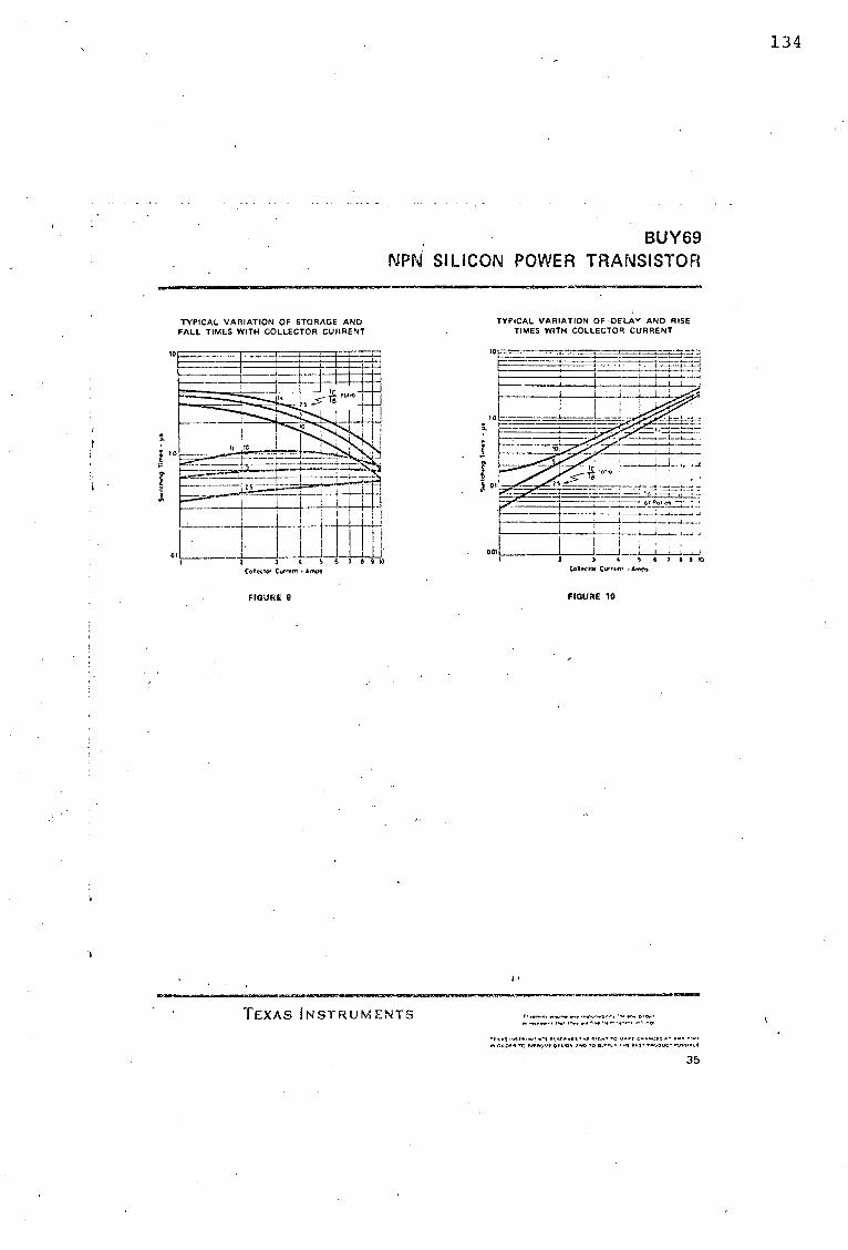
\1..
r j,
TYPICAL VARIATION OF STORAGE ANO FALL TIMES WITH COLLECTOR CURRENT
FIGURE 11
BUY69 NPN SI LICON POWER TRANSISTOR
,_
f "'
TYPICAL VARIATION OF ·DELA"' ANO RISE TIMES WITH COLLECTOR CURRENT
>--·----+---'-\ _ _;.; ~-_._-.. _· f-----L-... _~_.!,___.__.__ '--'-"
!--__ _,_I _ __.I _J ___ Ll_L_._J J J ' ~ 6 7 I I tO
Coll.cttv Curr,-n• - A""OS
FIGURE 10
.. TEXAS INSTRUMENTS fr r•"'"" .. ..,_ ..,,. ••O('<>"•b·•·•, '"' ..... r"~"
..... P'_ .. ,, ... , .................. f ................ ,._
•t.,•$ l'~T••~!.,.-t 11~!.C•'iitt .,.,, ••(;M• •c r,ur~ c .. ,. .... :f~ ,.. ,. .... , . .,,, lf'IOROf" TC ""'"lloQ'lf OfSIOl\ l'W'O '!'OSIJl'"l" <o<ff tf$"' •W.J.O~ '"°""''if\ 1
35
134

135
PRODUCT DESCRIPTION
The MCT26 is a NPN silicoi;i planar phototransistor coupled to a gallium arsenide diode~ It is mounted in a six leild plastic DIP.
PACKAGE DIMENSIONS
GOLO PLAT[O KOVAR NOTE: A.LL OIMENS!Or~s '""INCHES
ANO A~E TYPICAL E t.CEPT AS NOTED
C829
APPLICATIONS
• AC line/digital logic isolator
• Digital logic/digital logic isolator
• Telephone/telegraph line receiver
• Twisted pair line receiver
• High frequency power supply fe2dback control
• Reli!y contact monitor
• Power supply monitor
ABSOLUTE MAXIMUM RP\ TINGS Storage Temperature --55°C to 150°C Operating temperature -55°C to 100°C
Lead temperature (Soldering, 10 sec) 260°C Input Diode
Forward DC current .•••••..••..•. Reverse current •.....
60mA 10 µA
Peak forward current (1 µs pulse, 300 pps). . . .
Power dissipation at 25°C ambient Oerate linearly from 25°C .•....
3.0 A . 200 mW
2.6 mW/°C
Output Transistor Power Dissipation at 25°C ambrent .. ·. _ 200 mW Derate linearly from 25°C ...... __ 2.6 mW/°C
Input to output voltage. . . • • . . . . • l 500 volts Total f,ackage power dissipation at
25 C ambient (LED gilus detector) Derate linearly from 25 C .......•
. 250 mW 3.3 mW/°C
ELECTRO-OPTICAL CHARACTERISTICS (25°C Free Air Temperature Unless Otherwise Specified) CHARACTERISTICS MIN. lYP. MAX. UNITS TEST CONDITIONS
Emitter Forward voltage Reverse current Capacitance
Detector
~hFE BVCEO BVECO ICEO Capacitance Collector-emitter
BVcso lcso (dark)
Coupled DC current transfer ratio Bre,1kdo,·m vc>lla'.)e
Rcsi>tance emitter detector
VcE ls.it)
Capacitance LED to d.,•··<:t<H
Band·N;d1h ('>d''? f1<J1J'--' 5)
100 30 7
30
6 1500 300 1011
R1 .. 11 tir~lt' .1nd _Ltll ~-1:1 d ''"·•''"' .1pP1 tf:,··J -~ ~, .. , •. 1r·c~)
1.25 .15
100 300
150 75 1?. 5 8
100 1
14 2500
tOl :> 0.2 0.7 1.0 300
2
1.5 10
100
100
0.3 0.5 2.0
v l'A pF pF
v v
nA pF v
nA
% voe
n v v
pF kHt
IF~ 20 mA VR = 3.0 V V=O v c 1 v
VcE = 5 V, le= 100 pA le= 1.0 mA, IF= CJ le~ 10011A, IF= 0 VcE=5V,lf=O VcE =O IC= 10µA Vcn=5V,IF~o
VcE ~ 10 V, note 1
VAC, HMS@ f ~ 60 Hz
Vr:-o = 500 v IC·' 2!JOµA, IF= 20 mA •c "1.6 mA, If~ GO mA
le , 2 mA. not" 2
tc" 2 "-'~._v_c_f._ ~ _,_?_v. ·~(-"~_J __ _
J

MCT26 ..----------,,----------TYPICAL ELECTRO-OPTICAL CHARACTERISTIC CURVES
(25°C Free Air Temperature Unless Otherwise Specified)
< ~ 10.0 0: 0 .... u w t;; 7.5 0 I
.... z
5.0 w 0: a: :> u a:
,.5 0 .... ~ .... .... 0 0 <> .!' 0 10 15 20 25 30
Vet COLLECTOR VOLTAGE - DETECTOR IVOl.TSI
C830
Fig. 1 Detector Output Char;1cteristics
'°' ·- _.J.._JL/...J..-:=:.:t=:::r::=1:::::..i i .,,...-+--+---Jl'---+----l·-+--+---1 ~ n / lEOCURQENT.IO•nA ~
x
4 100 .!: a: 0 I-
~ 7.!> t;; 0 I .... ~ a: 0: :> u ..... 2.5 ~ 1-:> 0 .!'
............. _,._,_,._ .... Vcr·iO VOL lS ~ FR~( SlANOtNG 0['111((
~ u 1--t-+++ttttt·--i-t
a: 1 j I I ~-
a v ~ «-;·-+-::=:== ... --+--I-·-._,
" , ·~--t-;--+--il--+--t-+--1
c c 1.0 1--~-i·+tttt#-·-l-l
« t O .. •c-j "' 8 cu.
10 20 30 40 50 60 1, INPUT CURRENT - LED CmAI C831
Fig. 2 Input Current vs. Output Current
10•1---1--1--t
~ ICH1 >--+--1---t-·---l
!. ; 10-1
g 10·81----i---<I---<--<--·+.-.-+--<---<
« a. 10.9
" v :- 10.10
~ I() 111---+---<l,,...··-+--<·-+--+-t--l
10 •O 60 80 IM
C831
Fig. 3 Dark Current vs. Temperature re)
-60 _.O ·20 0 1"0 40 bO 80 100 AMB1(N1 l( .... P{AATURtrc1
IOK IC>()J< f"AEQU[NC¥ (H1)
0.! Cl.10.J0.4OCO-~1.0 1 J 4 ~'11 IC COLLECTOR cucmpH le lmJ\)
136
CS33
Fig. 4 Current Output vs. Temperature ·
C834
Fig. 5 Output ;'s. Frequency
C835
Fig. 6 Switching Time vs. Collector Current
I
CS.16
Fig. 7 Steady~State AC Voltage Limit of Isolation Dielectric
For additional characteristic curves, see figures 2, 3, 5, 6, 8, 11, 12, & 13 on MCT2.
OPERATING SCHEMATICS
PUL~E INPUT
470 Vee• 10VOLTS
DETECTOR
PULSE ·r. Ol/TPVT
l "• -1000
l
cs:ia
Modulation Circuit lhed to Obtain Output vs. Frequency Plot Circuit Used to Obtair; Switching Time vs. Collector Current Plot
NOTES
1. The current transfer ratio (le/IF) is the ratio of the detector coilector current to the LED input current with VcE at 101'olts.
2. The frequency at which ic is 3 dB down from the 1 kHz value.
3. Rise time (tr) is the time required for the co!/cct0< current to incmase from 10% of its final value to 90%.
Fall time (tr) is the cime requited for the co.'!ector cur~~-':_~-~'ec'-~::c from 90% or its in:tial value to 10%~-------J

APPENDIX 6 THE BEHAVIOUR OF THE COMPLETE CIRCUIT AT
TURN-ON
The complete response of any system may be resolved
into the natural and forced responses . For a first-order
L-R circuit :
~ + i R -- E sin ( wt + <fi ) dt s
The impedance functions are Z ( s) = R + sJ...
and Z(jw) = R + jwL
The forced response is
E E . . s s 1.f == ---:----~ -- ----
z ( j CJJ ) R + j wL
E smax ( -1 wL ) = ----------·-- • sin wt + ~ ··- tan R
l( R2 + w2L2
The natural response is obtained by setting Z{s) - O
Thus R s = - L
Assuming an exponential form of solution ,
_gt in --- Ae L
Taking the complete response as i - if + in
at time t = o+ , i = 0
Thus ,
0 =
Thus , A ·-
A(l) +
-E smax
E smax
I( R 2 + w2 L 2 )
sin(qi - tan
sin(~ - tan-l wL R
Substituting this value yields equation 3.23
-1 wL R
137

For the second-order R-L-C system ,
The natur~l response has a solution of the form ,
s = Ae-atsin(et + B}
where a = B.... 2L and o = /( . L R
2
LC - ~L2
The applied voltage at the instant of closing (t = 0) is
e = Essin<t>
138
At time t = O , the current i = O , and at t = o+, i = O , n n
since there must be continuity of current , thus th~ voltage
across the , Ve = 0
Thus
or
and
~i -· E sin<t> dt s
. di dt
E sin<j> s =---L
Asin(wt + B) - 0
A is finite ; thus S = O
'l'hus
and
then
di -at t A -at . et dt = Aee case - ae sin ~
E sinwt s Aecos(O) Aasin (0) - -L
E sin¢ A s = 0L
E 5
s.in<j> ·-ext •i = - . e sin et n 8L

The forced response yields
and from this
z ( j w) -- R + wL + l we
139
E
if s
= -1 rL - wL} • sin(wt + ~ + tan we )
/(R2 + rL wL} 2 ) -we Adding if and in above yields equation 3.25 •
Using the current notation of chapter 3 , the rigorous
solution is :
(il + i2) Rs + sLs (j_l + i2) + ici2 = E (1)
and (il + i 2 )R5
+ sL5(il + i 2 ) +RLil + sLLil = E (2)
(1) - (2)
!ei2 - (RLil + sLLil) = 0
or i 2 = i 1 se(RL + sLL)
Sub st. in ( 1) :
R
R8(il + i 1se(l\, + sLL)) + (il + i 1 sC(RL + sLL)sL
8 + ..... .
••••• + i 1 (R~ + sLL) = E
Setting Z(s) to zero
s3
eLLLLs + s 2eLLs~ + s2
eLLLRL + sCLRs11_. + sLL + Rs + RL = 0
Similarly a solution may be found around the i 2 loop .
140
APPENDIX 7 THE COMPLETE CIRCUI'r BEHAVIOUR AT TURN-·OFF
I is constant • Thus
I = i + i c t
Voltage across capacitor Ve .1 !t = ct 0
t T Capacitor current ic = I
where T = transistor turn-off time .
Thus :
Ve - I J tdt CtT
···. It 2 =
2CtT
which reaches a maximum value V
when t = T
s.ta9e 2
Staqe 3 ~""'·"'"--'"-
t = T
Final energy clearance
cm ax
i c
The circuit is reduced to the following
dt
The solution for the current as a function of time is
i(t) ~ Ae-o.tsin(et + ¢)
and
At t:i.me t = O+ i = I , the load current
Thus I ::: Asin<j>

and L s di dt =
di 1 = thus dt L s
(V + IR ) c s = A6cosip - Aasin<P
so that Acosip Rs
But a= -· 2Ls
Thus Acosip =
=
and tan<P -
A I ·- sin<P and
= Aecos<P - Ia
= l-cv + IR + L Ia) L
5e c s s .
1 IR L s s u<vc + IR + s 2L s s
1 3IR s Le(Vc +~
s L e s
3IR v + s c 2~
I = -1 wL
sin~tan v + 3IR ~ s c ~
Equation 3.29 follows from the substitution of the above
expressions •
141
APPENDIX 8 DESIGN DETAILS OF COMPLETE SYSTEM
A8.l THE POWER TRANSISTOR SWITCH:
The circuit may be broken into 3 separate units. These
are: The power transistor and its associated driver,
the feedback circuit and the interface to the control
pulse generator. Fig. 4.2 is reproduced here, with
these elements identified.
The "snubber" circuit comprises C~, Rl2 and D6.
Assuming a maximum load current of 10 A, a turn-off
time of the power transistor of 3 µsecs and a maximum
voltage rise of 150, we have
IT c = t 2Vcmax
10 x 3 x lo-6 = = 0,1 µF 2 x 150
During the turn~on time .of the freewheel switch, 5 µsecs,
the further voltage rise is
'LV 10 x 5 x lo-6
= = 500 v. 0,1 x io-6
This is clamped at 300 V by the zener diode D5, which
means that current flows in this diode for 3,5 µsecs (i.e.
rate of rise of 100 V/µsec). This results in 30 m Joules
being dissipated in the diode on each turn-off.
Assuming that the maximum voltage across the
capacitor during the "off" period is 206, and that the
surge current at turn-on is not allowed to exceed 10 A,
then
Vcmax Rl2 = I = 20 ohms
If the load current normally does not exceed 5 A, theJ?.
the maximum .current through the power transis.tor would be
142

M
';;)<
r-1
Con
trol
in
pu
t
. .
~
ple
te
po
wer
sw
itch
~·
4 2
. C
ircu
it
O-
com
_ -
"ig
. •
. -
I -a
og
~~--~-~~~~~T~T-•
I D
I~~--
~ ,._
1
. I
l i
IFe;db
-;;kl ~ l
I I
Inte
rfac
e ~56
j__
__
_
I _q_~
!_J,
,,. 129
T R1
I
' .
01
t-::-:
:;->
I .
: It¥
< I
t·R;I
I I ~c~
1 !
~c3:L.
:o.1.
, 0
I i_ _
_ L
.J..
J ./
~r-,
I I
1K5
. · -.
. '·?
.
, ..
1 I 1
D2
. '1
R12
l
\'-;
A
._.J
<.I
I'
>.' _
, l
I ~J
i 21':5
: .:c
/-·
. -;:
:C!_~~
-11-
R4
-: -:
i~ i 1
:';;:
03
'\Z
t--
r •
W,0
71
. F
ee
db
ack
I
. l
1.
~T:i l
i.8~1
D4 ~
*4
7.
lj 1
010
j 01
1 I
en
ab
le
I I
1K5
I .
R
T r C1
I .
H
r.,.1
,.,
,."v"
) I
-1
1{'
) -~
-,.
'
. .
39n~KI
R61
i=<9
~ c
1 a
1· I
33
ZS 1
,-
f>k1
_
-4
·Fee
dbac
k ~-!
w·-l-
----L
--T-L
-1 J
! I '
? I
I I
! 1
1-·1~v
erstaa
e -
I__:
__ 6
MA
lN S
WIT
CH
TER
MIN
ALS
/, <.
'§.
,,..
i
e=:
-rn
~~
R in
Q
.......
F '
ir ii ·
. ~_
_:.:
:_!,
_~!.
-
i

blowing the fuse. The operate time of the fuse is .
'immaterial, since the rise time of the current in the
thyristors is limited by lead inductance and must be
kept below 50 A/µsec for the devices employed. If
necessary, additional inductance is included in series
with the thyristors to achieve this. Turn-on delay for
the whole unit is 2µsecs. The use of a standard shunt,
with its stray inductance, tends to assist the operation
of the "crowbar" in the "faj_l-safe" direction, since the
voltage surges produced by the shunt speed up the com
parator operation.
F~g. A8.6 shows the circuit diagram of the com
parator trigg~r unit. A 711 dual comparator is con
nected as a double limit comparator, with the trip level
(usually 100 mV) provided by zener diode· Zl and potentio·
meter Pl. The 741 operational amplifier serves to invert
the voltage from Pl, providing thus both comparator
voltages. The output of the compaiator_gates the uni
junction transistor T3 which is coupled through trans
istor T2 to a pulse transformer. The pulse transformer
in turn triggers the thyristors. The capacitor C of the
U.J.T. circuit is fully charged when the comparator trips,
thus providing an immediate pulse at the detection of a
fault.
The performance of the unit is shown in the oscillo-
graphs AB.7 and AB.8 . The former shows the load current
with the "trip" point set at 5 amperes , while the latter
shows supply c~rrent . The successful diversion of the
current away from the load is very clear .
156

INPUT
o-=
150
2N2646
0,01 180
2,7K
10K 10K
8,2K
==~ 500
·5,6V Z1
100
~To S.C.R.
~Gates
2N2222
I '
==o
Fig. A8.6. Crowbar ; circuit diagram
157

. ' 158
Amp.
10 /JSec.
load current . The trip
Amp, r---"-
0-
0 500 fSec.

Pulse from VCO
\' I I •
l I
I
-~ I
' I I
. fJ1ll
I
1 )
152
Outputs
2 3 4 5 6 1) I) I) 1) 1}
153
.--
1,2K 33K 2
555 6 ') ..J
INPUT1.5K T2 5 2N2907
C5 BSX20
:!Ill
OUTPUT ,015 C1 1 0--
68K C2 4,7
1K ov
rc4 1K
68
8,21< 2N2222
7 c<l 1,5K 1.2~< (;l.'!.~
,001 +15V
· r_i9:,• A.8. 4. Pulse width controller circ~it diagr~
across R4 and thus a constant current in T2.
T2 Base voltage VB = RSVcc/(Rs + R6) = 1,7 Volts
T2 Emitter voltage VE _=:=~ 1,7 - Bbe =- ,1,0 Volts
T2 Emitter current = VE I R4 = l,o I 1200 = o, 8 mA
The voltage across Cl then rises as a linear ramp,
appearing at pins 6 and 7 of the 555 timer. __ This voltage
is also applied to the positive input of the 311 com
parator.
The pulse width control voltage is applied to the
negative input of the comparator through isolating re
sistor. RIO. When the voltage across _Cl exceeds the con
trol voltage, the compaiator trips. The output of the
comparator is level-shifted by transistor T3 and applied
to the "reset" terminal of the timer. Capacitor C is
then discharged and the process starts again.
Capacitors C3 and C4 bypass the reset line, to
avoid spurious oscillations of the comparator, while
capacitor CS decouples the power supply for the same
reason.
A simple solution to varying the duty cycle is to
apply the control voltage direct to pin 5 of the 555
timer. This pi=.:!rmi ts control over a limited range, in
sufficient for the wide range of variation considered
necessary in the prototype.
A8.5 'I'HE CURREN'r PROTE~TIOl'L ("CROWBAR") lHJIT:
The basic system is shown in fig. AB.5. When the voltage
drop across the shunt (a standard 100 mV instrument unit)
exceeds the trip level of the comparator, both thyristors
are triggered and the current is diverted to neutral,
154

155
Fuse Shunt '• I --0 - I I
IN TPUT
Trigger ..r-- Unit PUT ' OU i --
-- -·
Fi_5!. A8. 5. Crowbar block diagram

15 A, which i.s within the maximum ratetj. pulse current.
Duration of this current is the time constant of R12
c3
,
of 2 µsecs.
The power transistor Tl is driven by emitter-
follower transistor T2, with diodes Dl and D2 providing
a Baker clamp anti-saturation circuit. The diode Dl
must have a reverse voltage rating at least equal to the
maximum forward blocking voltage which Tl has to with-
stand. The maximum reverse voltage applied to D2 is the
reverse base-emitter bias of Tl, some 1,5 volts. The
current ratings of both diodes should equal the maximum
base current. The diodes selected were type MR826,
being of 600 V, 6 A rating. The turn-off time of these
diodes is 0,2µsec, which is short enough not to add
materially to the tµrn-off time of Tl. The reverse bias
to the base during turn-off is provided by resistor Rl
and diodes D3 - D5. Resistor R2 provides the return
path for this potential. The diodes D3 - DS are type
IN4001 operating with a steady current of 230 rnA supplied
by Rl. Capacitor Cl acts as a charge store.
Transistor T2, a type BD124, acts as an emitter-
follower driver for Tl. From available data, the current
gain of 3 A is typically 40. 'l'aki.ng the voltage drop
along the path base-emitter T2 - D2, base-emitter
Tl - D3 - D4 - DS as 4,7 volts (values of base-emitter
drops from Appendix 5), we have
Base current of T2 - = 75 mA
•rhus -- 1.50,6 0J·1n1s
' A preferred value resistor of 120 ohms was used to over-
come any spi:-ead in transi.stor characteri:::>t:i.c.;s.
144
The feedback circuit i.s coupled· to the power circuit
via capacitor C2 which, with resistor Rll and transistor
TS, together form the type of configuration shown in
fig. 13.14(b). The base-emitter voltage of TS functions
as a crude comparator. The zener diode DS serves to
limit the maximum voltage available and RlO iimits the
base current. Transistor T4 is the feedback enable
element. When T4 is hard on, TS is inhibited and no
feedback signal is able to activate the switch.
The maximum rate of rise of voltage across the
powe.r transistor is determined by C3, the "snubber 11
capacitor, and is, if the load current reaches a maximum
of 10 A, 50 V/µsec (from equation 3.27). The feedback
voltage is
and R11
c2
should be taj.1ored to obtain a feedback voltage
of say 5 volts at the lowest rate of rise of voltage. If
it is assumed that a voltage rise of S during· the turn-off
period, followed by a. further rise of 18 volts during the
freewheel turn--on, i.s not likely to cause any damage, then
I . m:i.n
= 2CtVcmax T
= 0,3 A
Thus the feedback circuit is not expected to operate .at
load currents below O, 3 A. 'l1he rate of rise of voltage
is 1,6 V/µsec.
·Thus
If c2 = 0,01 µF
The~ R11 = 310 n or nearest preferred value 330 •
The maximum feedback voltage, at say 10 A load current, is
e - 330 X O,Ol X 50 X 10-e X 106 - 165 Volts . fb -
which is clamped by D5.
145

Isolation for the driver stage is .provided by opto-
coupler OCl, a type MCT26, connected as an emitter-
follower with RS as load and R6 providing a return path
to ground for the base current. The photo-transistor
does not go into saturation in this connection and then
operates with a fall time of 2,6 sec. (See data,
Appendix S.) The transistor T3, a 2N2219, controls the
base of T2. (The nett result of this amplifier chain
is the control signals are inverted. That is, an input
to OCl turns Tl off and vice versa.) Resistor R4 limits
the base current supplied to R3.
Base drive voltag~ = RS X I ocl
RS = 1,2 Ka ; Iocl = 2 mA ·
Base drive voltage = 2,4 volts
-
and
2,4 vbe l.!-7. Ohms R4 - = Ib ~----
If the base Ib
current of T3 is limited to J.
R4 = 1700 ohms.
mA,
The preferred value of 1500 ohms was chosen.
then
The feedback circuit is enabled through opto-coupler
OC2. R7, R8 and R9 are derived from similar considerations
as R4, RS and R6. Transistoi T5, under control of T4 and
the feedback signal, diverts base current from T3 to turn
it off and hence turn Tl on~
A simple power supply rated at 15 volts a.nd 5 amps
drives the circuit.
The heat-sinking arrangements for the power trans-
istor are based on equation 3.28. The various parameters
are at worst-case values: .-
146

\'· ,r I
VMAX
VMIN
1MAX
1MIN
ts
=
-
=
-
=
400 Volts
3,3 Volts
s,o Amperes
1,0 rnA
25 secs
T = 1 millisec (That is, an operating frequency
of 1 FHz, maximum.)
t = 0,8 millisec (At 1 6Hz) on
Then P =
- 0,2 millisec (At l 6Hz)
(400X5X25Xlo- 6 ) + (3X3,3X5X0,8Xl0- 3 ) +
(3XlXl0- 3 )
= 29.,9 irvatts.
Which is well within the maximum alfowable dissipation of
the tiansistor (100 W).
The transistor operates in a pulsed mode, but since
the duty cycle range is likely to be very large, a worst-
case is postulated where the maximwn duty cycle is 80%,
and no allowance is made for the fact that this may very
often be lower for most of the transistor operating cycle.
'l'he thermal resistance from junction to case is not
stated in the manufacturer's specifications for the
BUY69, but since this device is contained in a T03
package, it may be assumed that this is 3 °c;w. The
maximum temperature rise of the junction above that of
the case is then
T. = 3,0 X 29,9 + 90 °c JC
The insulator between heat sink and transistor is
mica; using a silicon heat sink grease the thermal re-
sistance from heat sink to transistor is then 0,40 °c;w.
147

'I'he total thermal resistance from junction to heat sink
is then
0 . = 3, 0 + 0 I 40 = 3 '4 °c;w JS
The temperature rise of the junction above the heat
sink is then.
T. = 3,4 X 29,9 * 102 °c JS
·rf the maximum temperature of the junction is set
at 180°c, the maximum temperature rise of the heat sink
above ambient is then
T = 180 - 102 = 78 °c sa
This means that the thermal resistance of the heat sink
to air must be:
= 2; 6 °c/W
From the available data, this is provided by 100 mm of
the aluminium extrusion available.
A maximum case temperature rise.of 78°c results in
a dissipation derating to 70 watts; this leaves a com-
forta~le margin over the 30 0att~ needed to be dissi-
patedo (Fig. 4 of Appendix 5.)
No allowance is made for the fact l:hat the thermal
capacity of the heat.sink allows for transient overloads;
the transistor does not permit such overloads.
A8.2 VOL'I'AG E-CON'rROLLED OSCILLATOR:
The voltage-controlled oscillator is in essence a uni-
junction transistor relaxation oscillator with voltage-
controlled current supply to the capacitor. Fig. AB.l
shows a block diagram of the system. Referring to this
diagram for the nomenclature, we have that the capacitor
C is charged during the time T to reach the stand-off
voltage V of the U.J.T. which triggers and discharges c. s
148

Vin
0-
/
Rin
II•
180K . 5,6K
~---2N2219
120K -15V
'
Rt
Ct
IC --
8.2K
I•
E
.,,.,.., -
---r--o+15V
f220
4 . 0,001 -0
]
-- 261.6
C =0.022 I Pulse 22 output 1,8K
149

The voltage developed across the Bl resistance is the
pulse output. Then:
d = efb Rf Cf ·- e dt out
but e out d I out = or - e dt out c
=
thus efb
If A is very large,
Thus
or
= I -f -
= Vin R. in
-Vin R. in . . .
v s T
-
.T =
T 1 c f I out
0
or Pulse repetition frequency·=
dt
1 •r
i.e. a linear function of frequency.
= v.
l.D
R. cfv in s
The unijunction transistor chosen is a type 2N2646
with an intrinsic stand-off voltage of 7; with the
values of RIN and Cf chosen for the final circuit, shown
in fig. A8.2, an input voltage range of 0,7 to 1,4 gives
a frequency range of 300 Hz to 600 Hz.
The amplifier portion comprises transistors Tl, T2
and T3. The only noteworthy part of this circuit is the
use of the IN914 diode and 120 Kn resistor connected to
a -15 volt supply, which balances out the base-emitter
voltage drop of Tl. This enables the input voltage to
go to zero if necessary.
It might be added that voltage-controlled oscillators
are available at present in integrated circuit form; when
the work commenced on the prototype these were excessively
150

151
expensive and thus the design and construction of the
unit mentioned above was e1nbarked upon.
A8.3 GATED RING COUNTER:
The gated ring counter, fig. A8.3, comprises a synchronous
counter tising J-K bistables which is reset on the sixth
count. through a 6-input NANO gate. The outputs are de-
coded through 2-input NANO gates to give the waveforms of
fig. 4.4. A monostable multiv.ibrator triggered by the
v.c.o. provides the clock pulses for the counter.
A.l though the number of components could have been
reduced by using either a ripple-through binary counter or
a shift register with decoding, both of these configu-
rations introduce the possibility of a spurious pulse
entering the count. An additional pulse in the sequence
would have disastrous consequences for the system, causing
a short-circuit between supply phases.
A8.4 PULSE WIDTH CONTROLLER~
The pulse width controller varies the ratio between the
shunt and series switch conduction times, independently
of the frequency. The circuit diag·ram is shown in
fig. A8.4.
The 555 timer is triggered from the v.c.o. through
the pulse amplifier BSX20 transistor Tl. This stage is
required to provide the pulse polarity inversion re-
quired to trigger the 555.
Transistor T2, a 2N2907, provides a constant current
to the 4,7 F capacitor Cl. The base of T2 is kept at a
constant volt.a~.rc, thus rnaintaj_ning a constant voltage