Embed Size (px)
Citation preview
1

2
A Demonstration of Useful Electric Energy Generationfrom Piezoceramics in a Shoe
by
Nathan S. Shenck
Submitted to the Department of Electrical Engineering and Computer Science on May 21st, 1999in Partial Fulfillment of the Requirements for the Degree of Master of Science in
Electrical Engineering
ABSTRACT
The feasibility of harnessing electric energy using piezoelectric inserts in a sport sneaker has beendemonstrated. Continuing in that spirit, this thesis compares regulation schemes for conditioningthe electric energy harnessed by a piezoceramic source imbedded in a shoe insole. Two off-line,dc-dc direct converter hybrids (buck and forward) are proposed and implemented to improve theconversion efficiency over previously demonstrated conditioning schemes.
A rigid, bimorph piezoceramic transducer was developed and integrated into an off-the-shelforthopedic insert. The insert consists of two THUNDER PZT unimorphs connected in paralleland mounted on opposing sides of a Be-Cu backplate. The bimorph absorbs the energy of theheel strike and lift during walking, thereby inducing a charge differential across the faces of thePZT. The energy stored in this charge is removed at its peak and converted into a useful formusing a high-frequency switching technique.
The power conditioning circuitry consists of the following stages: Rectification, high-frequencyswitching (and step-down transformation), CMOS “555” timing and switcher control, low-sideoutput filtering, load stage on/off control, and output regulation. Finally, it is important to notethat, although the proposed conditioning scheme was designed for the transducer developedherein, it could be applied to any similar low-frequency, piezoelectric source.
Thesis Supervisor: Joseph ParadisoTitle: Principal Research Scientist and Technical Director, TTT, MIT Media Lab
C. S. Draper Laboratory Supervisor: Paul RosenstrachTitle: Program Manager

3

4
Personal Acknowledgements
There are many people I wish to thank for making the road to completing this projecta smoother one. Thank you…
Dick Gardner and John Sweeney for offering me this fellowship and giving me the chanceto study here in Boston.
Joe Paradiso and Paul Rosenstrach, my advisors, for your help and patience.
Steve Finberg, Carlo Venditti and Penn Clower for clearing many of the stumbling blocksalong the way.
All the friends I’ve made in Boston (even the Air Force ones), all my friends from Navy,and everyone at home -- I pray for many more years of good memories, friendship andservice.
The FAB -- Chiow, Clay, Cory, Eric, Tony and Weed… there’s really nothing I can saythat captures what you guys mean to me.
Mom and Dad, Aaron and Becky for your unconditional support and love. I honestlycould not be here with out you. Oh, and I’ll try to visit home more often, too… .
And to God, the Light unto my feet, who has never forsaken me despite my unworthiness.

5

6
[This page intentionally left blank]

7
Table of Contents1 Introduction 11
1.1 Motivation1.2 Background1.3 Objective1.4 Overview
2 The Piezoelectric Bimorph Insert 212.1 Overview of Piezoelectrics2.2 The THUNDER™ PZT Unimorph2.3 Bimorph Transducer and Insert Design2.4 Available Energy and Electromechanical Efficiency
3 Selection of a Power Conditioning Topology 473.1 Electrical Constraints3.2 Direct-Discharge Method3.3 Overview of Switching Converters and Topology Selections
4 Power Conditioning System 704.1 Ancillary Requirements and Constraints4.2 Electronic System Description
4.2.1 Input rectification and bootstrapping latch4.2.2 High-frequency switching, timer biasing and control4.2.3 Secondary-side filtering, load control and ON/OFF switching
5 Selected Components and Operating Parameters 955.1 Component Selections5.2 Switching Frequency and Transformer Design
6 Conclusions and Recommendations 1166.1 Results6.2 Conclusions6.3 Recommendations for Future Work
Appendix A Functional Description and Efficiency of Media Laboratory 129Conditioning Electronics
A.1 The Media Laboratory DesignA.2 Efficiency
Appendix B Matlab™ Script for Direct-Discharge Model 134
References 136

8
List of FiguresFig. 1.1: Schematic of power conditioning electronics and encoder circuitry for the MITMedia Laboratory shoe-powered RFID tag
Fig. 2.1: The modal axes with respect to poling direction p
Fig. 2.2: Two approaches to 31-mode piezoelectric energy scavenging in a shoe (graphiccourtesy of MIT Media Lab)
Fig. 2.3: Relationships for transverse compression/tension generator (31-mode)
Fig. 2.4: Outline of BeCu backplate and layout of THUNDER devices (to scale)
Fig. 2.5: Bimorph transducer (top view)
Fig. 2.6: Bimorph transducer (side view)
Fig. 2.7: Bimorph in the insert with heel pad shown
Fig. 2.8: 31-mode excitation in unimorph structure
Fig. 2.9: Equivalent circuit model for a piezoelectric source (at low-frequency)
Fig. 2.10: Bimorph transducer output into 500 kΩ resistive load
Fig. 2.11: Instantaneous power into 500 kΩ resistive load – 14.4 mW Avg.
Fig. 2.12: Rectified voltage signal into 500 kΩ Resistor – In boot
Fig. 2.13: Power into 500kΩ Resistor – In boot
Fig. 2.14: Current signal into 500 kΩ resistor – In boot
Fig. 3.1: Equivalent circuit for the “direct-discharge” architecture
Fig. 3.2: Energy delivered into various loads via direct-discharge (<Vl>=0V)
Fig. 3.3: Energy delivered into various loads via direct-discharge (<Vl>=9.7V)
Fig. 3.4: Block diagram illustrating switching converter operation
Fig. 3.5: Switch implementation in the direct down (or buck) converter with load

9
Fig. 3.6: The hybrid buck converter power conditioning system
Fig. 3.7: The hybrid forward converter power conditioning system
Fig. 4.1a: Buck converter power electronics system
Fig. 4.1b: Forward converter power electronics system
Fig. 4.2: Power required by ICM7555 biasing circuitry
Fig. 4.3: ICM7555 supply power at different operation frequencies (with 2nd orderequation of best fit shown)
Fig. 4.4: Comparator layout for dual MAX933 IC
Fig. 6.1: Forward converter signals at 1.3 mW and .8 Hz – continuous regulation
Fig. 6.2: Forward converter signals at 2.0 mW and .8 Hz – discontinuous regulation
Fig. 6.3: Bucket voltage with 36 steps using the bimorph insert
Fig. A.1: Schematic of power conditioning electronics and encoder circuitry for the MITMedia Laboratory shoe-powered RFID tag
Fig. A.2: Performance of the MIT Media Laboratory power conditioning system

10
List of Tables
Table 2.1: THUNDER™ “TH-6R” specifications
Table 4.1: Theoretical values for biasing components at 99.5% and 50% duty-cycles(Ct = 47 nF, Vcc = 4 Volts)
Table 4.2: Supply power data for ICM7555 at different operation frequencies (Vcc = 4Volts)
Table 4.3: Truth table for MAX934 in three-window configuration
Table 4.4: Truth table for NAND latch
Table 5.1: Active components
Table 5.2: Passive components
Table 5.3: Transformer specifications

11
Chapter 1
Introduction
The purpose of this work is to develop a piezoelectric shoe insert and complementary
conditioning electronics for unobtrusive, parasitic harvesting of the compression energy
normally absorbed by an insole during walking. Specifically, a boot insert with an
imbedded piezoceramic bimorph is developed, various power conversion schemes are
investigated, and two high-frequency forward switching converter hybrids are
implemented for conditioning the harnessed electrical energy. This chapter provides the
motivation, background and objectives for this work and concludes with a brief overview
of the remainder of the report.
1.1 Motivation
Consumer reliance upon body-worn electronic devices has risen significantly
throughout the past decade, and dichotic consumer demands for decreased size and
enhanced capabilities underscore a need for new ways to supply electric energy to these
devices. Traditionally, batteries have been sufficient, but this solution will become
increasingly less practical and inefficient as demands evolve. Further, chemical cells have
a limited lifetime, and their frequent replacement can be a costly annoyance.
Any viable supply solution to the emerging demand for unobtrusive, body-worn
devices must effectively address two tenets of remote power supply: storage and

12
distribution. Further, the only efficient and practical way to distribute the level of power
required by typical devices is through physical connection to a source. With that in mind,
two solutions emerge: either improve the energy density and reliability of local cells, or
utilize a centralized, body-worn energy storage unit with multiple distribution lines. The
first answer is the traditional approach – build a better battery. The second is cumbersome
and impractical.
Admittedly, the argument seems moot at this point as batteries serve the current power
demands adequately. Serious discussion of body-worn power packs and human-computer
interfaces may seem spuriously futuristic to some; however, that is not the case as many
such systems already exist and are becoming increasingly more a part of everyday life.
Pagers and PCS telephones are only the mundane examples of wearable technologies
which have realized wide-spread consumer use, and significant research is ongoing which
will carry the consumer into new arenas of human-machine interface. This growing
interest in body-worn electronics is evidenced further in the creation of the IEEE
Computer Societies’ Wearable Computer task force, the U. S. Army’s “Land Warrior
Program,” and a variety of other new low-power medical and military signaling
devices[1],[2].
If consumer reliance upon body-worn electronic continues to increase, both of the
above solutions to the power supply dilemma may prove insufficient or undesirable in
meeting future demands of a more “wired” society. Fortunately, however, as the power
requirements drop for many body-worn devices, a third solution emerges that eliminates

13
the distribution problem altogether -- develop and store electric energy at the load by
scavenging waste energy from a range of human activities. The average person spends a
significant percentage of his or her day on foot, dissipating a sizable portion of their total
energy into the environment. If this wasted energy were harnessed unobtrusively and
without affecting the normal actions of the body, the resulting freely-liberated electric
energy could be used in a variety of low-power applications. Pagers, health monitors,
self-powered emergency receivers, radio frequency identification (RFID) tags, and
emergency beacons or locators are a few examples of suitable low-power systems.
1.2 Background
Previous studies at the MIT Media Laboratory have explored the feasibility of
harnessing waste energy from a variety of body “sources”. One conducted in 1995
analyzed a number of common human activities and concluded that the heel strike during
walking is the most plentiful and readily-tapped source of this waste energy[3]. It
estimated that 67 Watts of power is available in the heel movement of an average (68 kg)
human walking at a brisk pace (2 steps per second with the foot moving 5 cm in the
vertical direction). Admittedly, it would be impossible to unobtrusively scavenge all of
that energy, but even a small percentage of it, removed imperceptibly, would provide
enough power to operate many of the body-worn systems on the market today. The study
further proposed a variety of methods to harvest this energy, including a piezoelectric
(PVDF) film insert and a coupled resonant magnetic generator. A second Media
Laboratory study amplified the assertion that shoe energy could easily be tapped and

14
suggested a system of embedded piezoelectric materials and miniature control
electronics[4]. It observed that a shoe or boot, because of the relatively large volume of
space available in the sole and heel, would make an ideal test bed for the concept of body
energy harvesting.
Since these studies were published, the Media Laboratory has further explored
parasitic power harvesting in shoes, and a more in-depth comparison of three shoe-worn
devices was performed[5],[6]. Two of the devices tested were piezoelectric in nature: a
flexible, multi-layer PVDF film stave mounted under the insole along the ball of the foot,
and a THUNDER composite PZT unimorph fitted above the insole at the center of the
heel strike region. The third was an externally mounted rotary magnetic generator. The
merits and disadvantages of each system were discussed, a comparison of the energy
output and basic source characteristics was made, and a handful of suggested applications
and possible design improvements were provided. Finally, two shoe-powered, 12-bit,
RFID encoder/transmitters were built as demonstrations designed around the piezoelectric
sources.
Each of these devices were effective in converting waste mechanical energy into useful
electric energy; however, all of the systems displayed compromises commensurate to their
merits. While it was the most easily integrable and least invasive of the three technologies,
the PVDF stave’s raw power output (1.1 mW into a 250 kΩ resistive load) is severely
limited by the low electromechanical efficiency of this implementation. It is believed that
the efficiency of this device could be improved, however, by more effectively inducing a

15
31-mode longitudinal strain along the PVDF stave using some innovative mechanical
structure. (A brief discussion of relevant piezoelectric theory is found in Sect. 2.1.) The
PZT unimorph produced slightly more raw power under the same excitation (1.8 mW into
same load), but the unimorph is more fragile and therefore not as easily assimilated. The
conventional rotary generator was certainly the most powerful and efficient of the devices
tested, providing enough energy to operate a transistor radio and drive a small speaker.
However, this “lumpy” design interferes with the normal walking gait and is obtrusive and
unsightly.
The only notable shortcoming among the three systems is the inefficiency of the power
conditioning electronics used in the two piezoelectric RFID demonstration circuits. While
sublime in its simplicity and low quiescent power requirement, the original Media
Laboratory design is generally not well suited to the electrical characteristics of a
piezoelectric source excited at the frequency of a brisk walk. In both cases, this circuitry
consists of a four diode full-wave rectifier, a short-term storage capacitor that is valued
(by necessity of the design) nearly three orders of magnitude greater than the capacitance
of the source, a novel “latched-SCR” trigger for load switching, and a micro-power,
commercial linear regulator. (See Figure 1.1.)

16
Fig. 1.1: Schematic of power conditioning electronics and encoder circuitry for the MITMedia Laboratory shoe-powered RFID tag[5]
The average power output and efficiency of the Media Lab power conditioning
circuitry was calculated, and it is included in Appendix A along with a brief functional
description of the circuit. Simply stated, the great disparity between the source
capacitance and short-term storage capacitor C1, and the virtual “voltage clamp” function
performed by the load switching stage, make leaking charge from a piezoelectric source
into a capacitive “bucket” (termed direct discharge throughout this report) an extremely
inefficient process. Further, all linear regulators incur a penalty in efficiency -- especially
when the ratio of Vin to Vout is much less than unity -- because their average input and
output current values are approximately equal (ignoring quiescent current). The Media
Laboratory study concludes by acknowledging that work remains in this area.

17
1.3 Objective
The objective of this thesis is to continue the work outlined above, proposing power
conditioning systems which more efficiently harness electric energy from a piezoelectric
source imbedded in a shoe. A rigid piezoceramic bimorph transducer was designed and
integrated into an off-the-shelf orthopedic insole, thereby creating a more rugged, self-
contained piezoelectric boot insert. Further, two off-line buck and forward switching
converters are presented, consisting of a small number of inexpensive and readily-available
components and materials. The performance of these converters is evaluated and their
efficiency compared to the previous design.
The source characteristics and boundary conditions upon the piezoelectric system
presented herein are much different than those normally encountered in switching
converter applications. Therefore, much of the theory and practice common to switching
converter design does not apply. Specifically, the following points should be kept in mind
while reading this report:
• Because a low-frequency piezoelectric source is essentially a capacitor and aparallel charge source, and Ec= ½CV2 describes the energy stored on a capacitor,it is advantageous to allow the source voltage to peak before removing the energy.
• The charge liberated per step cycle is relatively constant under the same loadingforce, regardless of walking speed.
• Output ripple is dominated by the low excitation frequency of walking. Therefore,output filter component selections must be based upon different criteria than usual.Further, a large output capacitance ( > 100 µF) must be included simply to keepthe ripple voltage within acceptable limits.
• Duty cycle control is not an issue – the switching converter is implemented toprovide current gain (i.e. a better impedance match between a high-voltage, low-current capacitive source and low-voltage storage capacitor).

18
• Because these systems are low-power and average source current is very low,semiconductor switches are selected to minimize gate charge, not ON resistance.
• Switching frequencies are chosen to minimize system energy loss, not filtercomponent dimensions.
1.4 Overview
Chapter 2 discusses the design and electrical characterization of the bimorph
piezoceramic transducer. It provides a basic introduction of piezoelectric theory and
terminology and a brief derivation of the physical principles involved in bending 31-mode
electromechanical transduction. The THUNDER PZT unimorph was chosen for this
application because of its higher energy density and commercial availability. (The PVDF
stave previously described was designed and developed by the Media Laboratory in
collaboration with researchers at AMP Sensors, now a part of Measurement Specialties,
Inc.) Modifications to the THUNDER unimorph, construction of the rigid bimorph
transducer developed herein, and their integration into a boot insole are discussed.
Finally, a source model is derived for the bimorph, raw output power is determined, and
the electromechanical efficiency is calculated.
Chapter 3 compares a variety of power conditioning architectures. It discusses the
relative merits of resonant shunting, voltage-limited “direct discharge” (the original Media
Laboratory technique), and the application of an off-the-shelf, dc-dc switching controller.
It develops the reasoning behind using a hybrid high-frequency switching converter and
outlines the control functions required for low-power operation. Finally, it compares two

19
switching down converter topologies, the buck and the forward converter, and presents
two systems based upon these topologies for use with a piezoceramic source.
Chapter 4 discusses the power conditioning electronics proposed here. It begins by
enumerating the ancillary requirements and constraints on the design and provides a
functional description in the following stages: 1) input rectification and bootstrapping
latch, 2) high-frequency switching, timer biasing and control, and 3) low-side filtering,
load control and ON/OFF switching. Further, it develops each of these stages for the two
converter topologies.
Chapter 5 outlines the methodology for selecting specific components and
determining the key operating parameters including switching frequency and duty cycle.
An optimization curve (for power loss) is provided for the ICM7555 CMOS timer, the
MOSFET switch, the transformer and the inductor.
Chapter 6 discusses implementation and results for this work. It outlines the
shortcomings of the two switching systems herein proposed and provides conclusions on
efficiency and efficacy of the approach. The concept of applying switching converters in a
shoe-worn piezoelectric power systems is proven, but the electronics designs need further
refinement. The forward converter yielded 1.48 mW with a regulated 3 Volt output, or
17.6% electrical efficiency; the direct converter was much less efficient and converted
slightly more than enough power to support its own electronics. Finally, the chapter

20
concludes by enumerating areas requiring further attention and proposes related future
work based upon these results.

21
Chapter 2
The Piezoelectric Bimorph Insert
The following chapter provides background theory and design methodology for the PZT
bimorph insert developed in this project. It begins with a brief overview of pertinent
piezoelectric theory, discusses the THUNDER™ PZT unimorph transducer and the
bimorph insert developed therefrom, and derives an equivalent circuit model for this
device as a low-frequency power source. Finally, this chapter presents the raw output
energy before conditioning and the electromechanical conversion efficiency of the
transducer.
2.1 Overview of Piezoelectrics
Interest in piezoelectric crystals, ceramics, and films has grown rapidly over the past
two decades as new applications in active control systems and transducers have emerged.
It has been shown in a variety of aerospace applications that the electromechanical
coupling properties of these materials can be utilized for active structural damping of high-
frequency dynamics[7]. Further, piezoelectric materials have been used extensively as
passive transducers in microphones, submarine hydrophones, and strain gauges, and as
resonators in electric oscillators and high-frequency amplifiers. A wide variety of crystal
and flexible film types exist today, most of which are inexpensive, easy to manufacture and
adapt, and display well-documented electromechanical properties.

22
The piezoelectric effect — a material's capacity to convert mechanical energy into
electrical energy, and the inverse — is observable in a wide array of crystalline substances
which have asymmetric unit cells. When an external force mechanically strains a
piezoelectric element, the ions in these unit cells are displaced and aligned in a regular
pattern within the crystal lattice. The discrete dipole effects accumulate, resulting in an
electrostatic potential developed between opposing faces of the structure[8]. Relationships
between applied force and the subsequent response of a piezoelectric element depend
upon three factors: 1) the dimensions and geometry of the element, 2) the piezoelectric
properties of the material, and 3) the directions of the mechanical or electrical excitation.
To designate these directions, a 3-dimensional, orthogonal modal space is defined. The
various electromechanical modes identify the axes of electrical and mechanical excitation,
where electrical input/output occurs normal to the ith axis, and mechanical input/output
occurs normal to the jth (See Fig. 2.1). For example, the 31-mode mechanical excitation
signifies transverse mechanical strain normal to the 1 axis, inducing an electric field normal
to the 3 axis. Finally, the induced electric field will be normal to a given polling vector p,
defined by applying a high potential electric field though the material during the
manufacturing process. This process is known as polling the piezoelectric, and must be
performed while the material is heated above its Curie temperature[9].

23
p 2
1
3
Fig. 2.1: The modal axes with respect to poling vector p
The 31-mode of operation is most appropriate for harnessing waste energy in a shoe
because the dimensions of the insole limit the shapes of materials which can be integrated
without loss of comfort or a radical change in shoe design. A thin, flat, piezoelectric
element is a natural solution given the these constraints. Commonly, this piezoelectric
material is excited in 31-mode operation by flexing the plate about its neutral axis, thereby
inducing elongation or compression at the faces. Parallel compression, or 33-mode
excitation, although intuitively attractive is not practical because of the material properties
of rigid piezoelectric materials (a high Young’s modulus and low electromechanical
efficiency in 33-mode) and the limited forces produced during walking [3]. Thus, there
traditionally have been two principal means by which shoe power is piezoelectrically
scavenged in bending 31-mode excitation. One previously demonstrated method is to tap
the changing curvature experienced at the ball of the foot using a multilaminar, flexible,
polyvinylidene fluoride (PVDF) stave mounted under the insole. Another is to use the
heel strike to flatten a pre-stressed, curved piezoelectric sheet or button in the heel; the
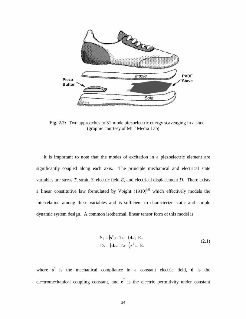
later is applied in this design (See Fig. 2.2).
24
Fig. 2.2: Two approaches to 31-mode piezoelectric energy scavenging in a shoe(graphic courtesy of MIT Media Lab)
It is important to note that the modes of excitation in a piezoelectric element are
significantly coupled along each axis. The principle mechanical and electrical state
variables are stress T, strain S, electric field E, and electrical displacement D. There exists
a linear constitutive law formulated by Voight (1910)[9] which effectively models the
interrelation among these variables and is sufficient to characterize static and simple
dynamic system design. A common isothermal, linear tensor form of this model is
( ) ( )( ) ( ) mnm
Tklnkln
mmijkljklE
ij
ETD
ETS
ε+=+=
d
ds(2.1)
where sE is the mechanical compliance in a constant electric field, d is the
electromechanical coupling constant, and εT is the electric permitivity under constant
PiezoButton
PVDFStave

25
stress. Fortunately, by isolating excitation and poling to a single mode and making a few
other reasonable assumptions, simple, practical relationships are derived. One notable
convention involves the coefficient dij, commonly expressed in C/m2 per N/m2.
)( stress mechanical applied)( field-Econstant in density charge
ji
TD
dE
ij == (2.2)
When the applied force is distributed over an area fully covered by surface electrode, the
units of area cancel and the coefficient directly relates charge to unit force, or C/N. This
simplification is particularly useful when contemplating a piezoelectric element as a charge
source. Another important convention is the relationship between an applied mechanical
stress and the resulting open-circuit electric field, gij, expressed in V/m per N/m2. In this
way, output voltage can be found from the calculated electric field and the thickness of the
active material between the electrodes.
)( stress mechanical applied)( field-Ecircuit open
ji
TE
gD
ij == (2.3)
These previous equations lead to the simplified generator/transducer relationships for
31-mode mechanical excitation found in Eqns. 2.4a and 2.4b with parameters defined in
Fig. 2.3, and are the basis for later calculations.

26
+ p_
+Q or V
-F
+ p_
-Q or V
+F
+ p_ WL
T
Fig. 2.3: Relationships for transverse compression/tension generator (31-mode) [8]
TWFd
LWQ 31= (2.4a)
TWFg
TV 31= (2.4b)
Where,
direction PolingLengthWidth
Thicknesspotential Plate
force lateral Appliedcharge Liberated
===
====
pLWTVFQ
At excitation frequencies well below mechanical resonance, the voltage and charge
coefficients discussed above are related to the relative permitivity of the material in the
following manner:
ijoTijij gd εε= (2.5)
or, in the 31-mode case,

27
FVW
LFQT
oTijεε= (2.6)
yielding
VCQ 31= (2.7)
Therefore, it is shown that when operating in 31-mode at frequencies below the
mechanical poles of the system, a piezoelectric device can be modeled as a parallel plate
capacitor. The final coefficient germane to this work is the electromechanical coupling
constant kij -- a measure of the conversion efficiency from mechanical to electrical energy
(or vice verse). It is the square root of the ratio between stored converted energy and
required input energy.
)(energy mechanical applied)(energy electrical storedj
ikij = (2.8)
2.2 The THUNDER PZT Unimorph
The THUNDER or “Thin-Layer Composite Unimorph Ferroelectric Driver and
Sensor,” is a based upon a piezoceramic manufacturing process originally developed by
NASA Langley in conjunction with the RAINBOW (Reduced and Internally Biased Oxide
Wafer) design effort[11]. This technology was licensed to Face International Corporation,
who manufactures the high-efficiency THUNDER piezoelectric sensor/actuator using the
NASA process. The transducer consists of a pre-stressed spring steel base plate, several

28
layers of aluminum and silicone-based adhesive film-form, and a PZT (Lead zirconate
titanate) Type 5A wafer. The materials are assembled so that the PZT wafer is
sandwiched between the aluminum and adhesive dielectric film. This composite is then
bonded to the spring steel back plate, thermally processed at 320°C in an autoclave, and
electrically poled in a high-voltage dielectric immersion[12]. The resulting piezoceramic
unimorph has a higher electromechanical coupling coefficient than common piezoelectric
films (e.g. polyvinylidene fluoride film, or PVDF) but is flexible enough to be used with a
reasonable displacement in 31-mode excitation.
THUNDER transducers are commercially available in a variety of sizes and force-
displacement characteristics, each with very different electromechanical characteristics.
As discussed previously, the power available from a flat piezoelectric transducer under 31-
mode bending excitation is generally proportional to the volume of the material and the
vertical displacement induced. Therefore, while constrained by the size, comfort, and
vertical displacement experienced by the heel of a shoe insert, the volume of PZT
piezoceramic was maximized when selecting the appropriate transducer. Hence, the “TH-
6R” device was chosen; its specifications are shown in Table 2.1.
THUNDER™ "TH-6R" SpecificationsWeight (g) 16.3Dimensions (mm) 76.2 x 50.8 x .635PZT thickness (mm) 0.381Static Capacitance (nF) 76Maximum Voltage (V) 320Resonant freq. (Hz) 47Vertical disp. (mm) 4.8
Table 2.1: THUNDER™ “TH-6R” specifications[13]

29
THUNDER devices were used in previous shoe-worn power scavenging systems
demonstrated by the MIT Media Laboratory, and they showed promising results. They
were selected for use in this project for many of the same reasons: They are of the
appropriate size for shoe integration, are commercially available, and have a much greater
energy output per unit volume than any similar device found on the market. Before
development of the technology used in the fabrication of these transducers, ceramic
elements were wholly unsuitable for integration into a shoe power harvesting system.
Piezoceramics have a much better coupling efficiency and favorable impedance
characteristics when compared to their flexible film counterparts; however, in a raw form,
they are far too brittle for 31-mode excitation[14]. THUNDER devices display the best
qualities of the two material types. There are still some severe limitations in allowable
vertical displacement and in general ruggedness, but these shortfalls can be overcome
using simple support structures like the ones discussed in the proceeding section.
2.3 The Bimorph Transducer and Insert Design
This section enumerates the materials and methods used in constructing the bimorph
insert. The intent was to develop a rugged bimorph for integration into an off-the-shelf
shoe insole. A bimorph construction is appropriate for a number of reasons. Primarily,
the vertical displacement of TH-6R transducer is quite small (4.8 mm, maximum), and
there is enough room in the heel cup of most insoles to place an opposed pair of these
devices mounted on a thin backplate. Also, by connecting the transducers as parallel

30
sources, not only is the available energy doubled, but the source impedance characteristics
are improved as well. Finally, a bimorph transducer is more rugged and comfortable
because it naturally suspends itself in the hollow pocket of the insole, thereby better
adapting to various distributions of weight and velocity of the footfall and providing a
greater displacement through which the heel decelerates.
The following materials were used in constructing the PZT bimorph and insole:
1. (2) THUNDER™ “TH-6R” PZT transducers with trimmed base plates2. (1) Backplate -- .025” (.635 mm) BeCu metal sheet cut to appropriate shape
(See Fig. 2.4)3. (2) .10” (2.54 mm) diameter Al rivets4. Silver conductive epoxy5. Uralane® 5750 Urethane Conformal Coating/Epoxy6. (3) ~2.5’ (76.2 cm), 24 awg, stranded Cu wire7. (1) Tuli “Mercury’s Shadow” orthopedic shoe insole (Men’s 9-11, right)
Using a sheet metal trimmer and fine grain files, the edges of the THUNDER devices
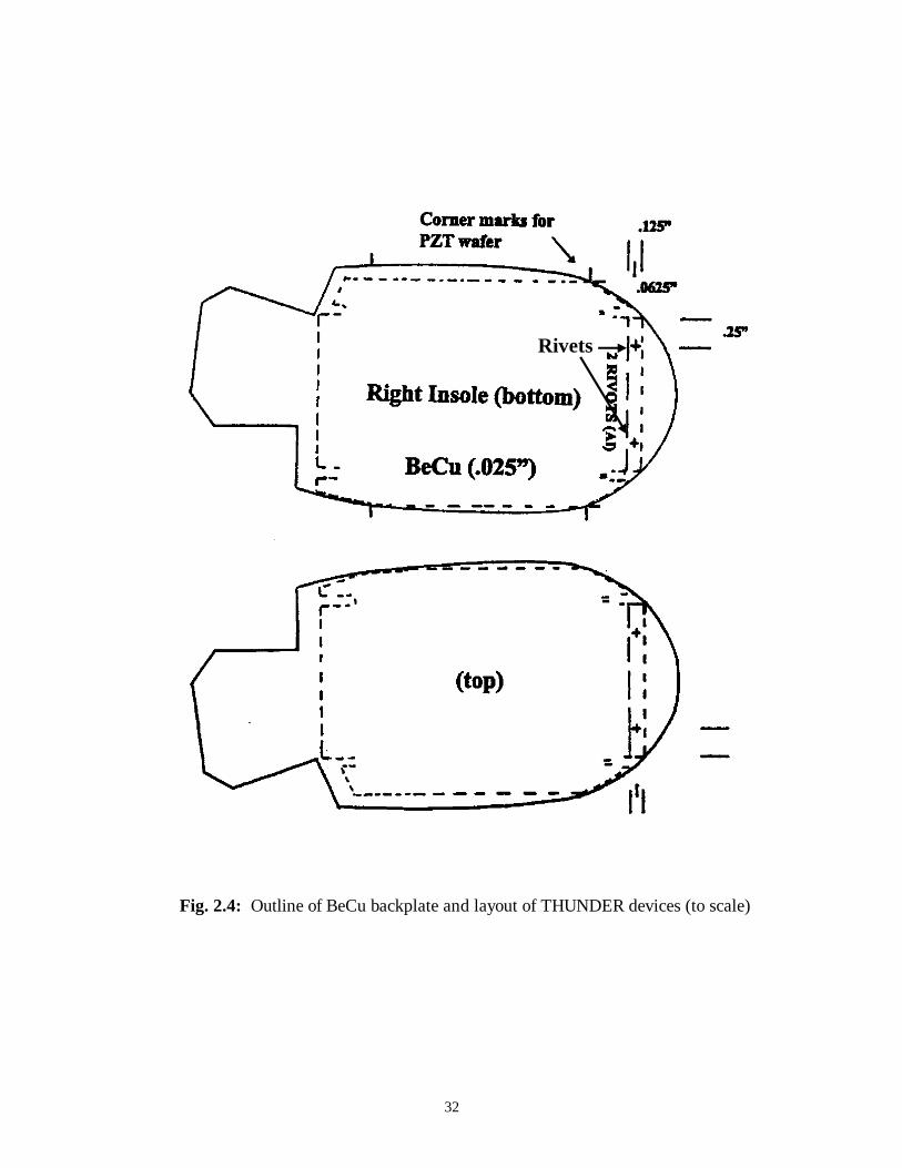
were trimmed to fit properly on the BeCu backplate. A scale outline of the backplate is
shown in Fig. 2.4 on the proceeding page, and the layout of the trimmed THUNDER
devices is highlighted with a dashed line. These transducers were mounted to the
backplate as shown using two aluminum rivets, and the tops of the rivets were filed down
to reduce the profile of the device. After mounting, the bond between the spring steel
backing and edges of the PZT wafer was reinforced with an elastomeric epoxy, Uralane
5750, applied using a jeweler’s oiler. The epoxy was cured at 135° F for 3 hours. In
previous bimorph designs, the edges of the PZT wafer had a the propensity to separate
from the spring steel and crack, degrading performance and changing the electrical

31
characteristics of the device. By reinforcing these trouble spots with a semi-rigid epoxy,
this failure has not occurred in later designs.
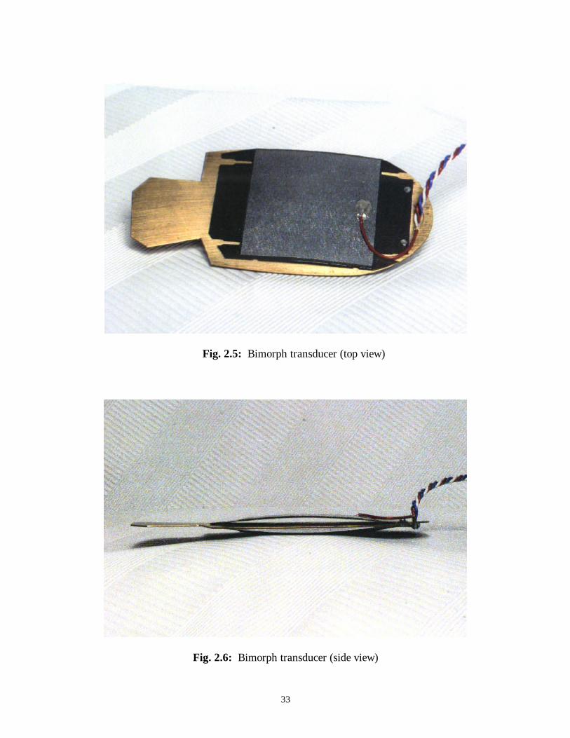
Wire leads were bonded to the exposed aluminum electrode coatings one both sides of
the bimorph using silver epoxy, and the epoxy was cured at 135° F for 4 hours. A third
lead was soldered to the BeCu backplate, and all three leads were woven through 3 holes
drilled in the aft section of the backplate. (See Figs. 2.5 and 2.6.) No explicit electrical
connection was made between the steel base plates of the two THUNDER devices – they
are firmly attached to the conductive backplate by the aluminum rivets, and an electrical
connection of sufficient quality has been observed.
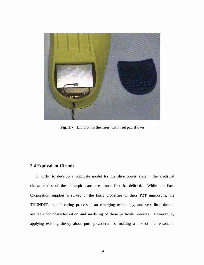
Finally, a cavity of appropriate size was hollowed out of the Tuli insole by first
removing the blue heel cushion from the yellow body of the insert and then hollowing a
recess into the forward portion of the insert. (See Fig. 2.7.) The bimorph was then
placed into the insole, trimming portions of this insole if necessary for fit, and the heel
portion was resealed.
32
Rivets
Fig. 2.4: Outline of BeCu backplate and layout of THUNDER devices (to scale)
33
Fig. 2.5: Bimorph transducer (top view)
Fig. 2.6: Bimorph transducer (side view)
34
Fig. 2.7: Bimorph in the insert with heel pad shown
2.4 Equivalent Circuit
In order to develop a complete model for the shoe power system, the electrical
characteristics of the bimorph transducer must first be defined. While the Face
Corporation supplies a survey of the basic properties of their PZT unimorphs, the
THUNDER manufacturing process is an emerging technology, and very little data is
available for characterization and modeling of these particular devices. However, by
applying existing theory about pure piezoceramics, making a few of the reasonable

35
assumptions discussed in the previous section, and conducting a series in-lab experiments,
a suitable equivalent circuit is developed.
It is first assumed that the THUNDER transducers which make up the bimorph insert
operate principally in the 31-mode, and that charge contributed by other modes
(specifically, 33-mode bulk compression of the PZT wafer under the weight of the bearer)
is serendipitous but insignificant to these calculations. As stated, the THUNDER devices
consist of a wafer of PZT bonded to a strip of spring steel, whose Young’s modulus is
better than two orders of magnitude greater than the modulus of PZT[15]. Therefore,
flattening the pre-strained unimorph by applying a force from above, along the vertical
axis, will compress the PZT material along the horizontal direction to a degree
proportional to the initial radius of curvature and distance from the spring steel base plate.
(See Fig. 2.8.)
∆r
FF
-
1
+
p
F
2 (-)
3
Neutral Axis
Fig. 2.8: 31-mode excitation in unimorph structure

36
The strain experienced by any point within a cantilever beam of uniform thickness
along the 3 or z axis in the previous drawing is a function of the radius of curvature R and
the distance D from the neutral axis of the beam (the PZT surface bonded to the spring
steel base plate in this design)[16]. For simplicity, the 1, 2 and 3 axes are mapped into the
Cartesian x, y and z, respectively, for the following derivation.
)(1
),,(),,(),,( 2
2
xRzyxD
xz
zyxDzyxS ⋅−=⋅−=∂∂ (2.9)
Further, given the symmetry about the x and y axes, the relationship for the bulk elastic
modulus, and Eqns. 2.4, the following force gradient is found within the PZT wafer:
z
zxzx R
DAYDFSA
F
STY ∆⋅−=∆⇒== )( (2.10)
In words, the magnitude of the transverse force in the x direction is proportional to the
discrete area Ax through which the force acts, the distance Dz from the neutral axis, and
the inverse radius of curvature R in the z direction. Now, by introducing the piezoelectric
relationships for bending 31-mode operation,
( )
∆
∆−=∆⇒=
z
z
RD
TYWT
LdQ
TFLd
Q 3131 (2.11)

37
And, integrating the strata of charge accumulation through the range of Dz
z0 31 dD
−= ∫
z
zT
RD
YLWdQ (2.12)
yielding
( )
−=
zRT
LWTYd
Q2
31 (2.13)
The result above shows that the total charge liberated during compressing or
relaxation of the transducer is related to the material properties of PZT, its volume, and
the ratio between the thickness T (z direction) to the induced radius of curvature. Further,
it assumes that the mechanically neutral state of the beam is ‘flat,’ but the THUNDER
unimorph is neutrally curved. Since these devices are operated between flat and curved
end states, however, the total charge calculation for either of those end states (assuming
complete discharge at the previous state) will be the same. That calculation is performed
by finding the absolute difference of the total charge at the two states, or
( ) ( )
−
=
max
31
min
31t R
TLWT
2Yd
RT
LWT2
YdQ (2.14)
and, when R→ ∞ at flatness,
( )
=
min
31
2 RT
LWTYd
Qt (2.15)

38
Finally, because the radius of curvature is much larger than the thickness and length of the
piezoceramic beam, the following assumption, common to derivations in beam mechanics
for simply supported beams, is made[9]:
R
Lzd 8
2
= (2.16)
yielding
( )
= 2
31 82 L
TzLWT
YdQ d
t (2.17)
where zd is the vertical displacement of the center of the beam from neutral.
The previous derivation is important because it reveals that the total charge
produced by the transducer is directly proportional to the vertical displacement at its
center. Therefore, the rate at which charge is produced by a footfall corresponds linearly
to the velocity with which the displacement is introduced on the transducer. The energy
conversion process is thus appropriately modeled at this low frequency as a finite, ramped
charge source which reaches its peak charge at the end of each cycle.
Because they are excited by 31-mode bending and the excitation frequency is
significantly below the mechanical poles of the device, the THUNDER transducer can be
thought of simply as a parallel plate capacitor -- the stainless steel backing and the
aluminum top face form the two plates, and the PZT wafer and SI-based adhesive serve as
the separating dielectric[18]. As suggested above, energy conversion is modeled as a

39
charge source, and the dielectric leakage is represented by a resistor, both in parallel
connection with the capacitor[19]. This model is typically used to characterize the low-
frequency operation of piezoelectric devices as sensors. The equivalent circuit model
follows:
↑ qp(t)
+
-
vo(t)Cp Rd
Fig. 2.9: Equivalent circuit model for a piezoelectric source (at low-frequency)
The relative dielectric constant for PZT (at a constant stress) is strictly a material
property and is given by εT31, whereas the static capacitance is given by[10]
TLW
C=T
o 31εε (2.18)
It is important to note, however, that dielectric constant of piezoceramic material changes
as a result of the THUNDER manufacturing and poling process, so it is not sufficient to
rely upon the above equation and published values for the dielectric constant of PZT-5A
when determining the capacitance of the transducer. Rigorous impedance measurements
have been performed from which the capacitance through a range of frequencies is
obtained[12]. These measurements show that the THUNDER “TH 6-R” device has nearly
the same static capacitance, 70-80 nF, from dc through 600 Hz and again above 1 kHz.

40
Further, the capacitance of the bimorph source was determined (at both 1 kHz and 10
kHz) to be 143 nF. That value is intuitively tenable given the bimorph insert is a parallel
electrical connection of two “TH 6-R” devices.
2.4 Available Energy and Electromechanical Efficiency
The available electrical energy from the bimorph transducer can be determined in two
ways – either by calculating the theoretical energy stored on a capacitor for the peak
voltage induced on the device or by acquiring signal data through a known load. In the
first case, knowing that the energy stored in a capacitor is given by
2peakpc VC
21
E = (2.19)
where Cp is the source capacitance and Vpeak is the voltage at full compression. The
energy available with each compression or relaxation, assuming that all charge is poled
from the transducer between physical endpoints, was determined by measuring the open
circuit voltage across the poles of the device at full compression. A test circuit was
constructed by connecting in series the bimorph transducer, a 30 MΩ load, the leads of an
oscilloscope probe (10 MΩ ), and a push-button momentary switch. The transducer was
placed in a padded bench vice, and before each compression, the its leads were
momentarily shorted circuited to ensure that there was no charge accumulation across the
PZT faces. The vice was then tightened until the transducer faces were fully flattened to

41
the backplate. Once the transducer was compressed, the momentary switch was
depressed and the peak source voltage (actually .25Vpeak because of the ¼ voltage divider
construction of the test circuit) and subsequent exponential decay were recorded on the
oscilloscope. This procedure was performed as quickly as possible to limit the effects of
dielectric leakage upon the accuracy of the voltage measurement. The average peak
source voltage was found as approximately 306 Volts, and the electric energy available at
each compression (or relaxation) across a 143 nF capacitance is calculated as
mJ 6.69=⋅⋅⋅= − 29c 306)10143(
21
E (2.20)
Further, using an average 3/5 Hz stepping frequency[3] and assuming that the
developed charge is fully poled two times during each cycle (compression and relaxation),
the anticipated average electric power available from cyclic excitation of the unimorph is
mW 8.03=⋅⋅=53)00669(.2elecP (2.21)
Or, using the average walking frequency of the test subject, providing for better
comparison of theoretical and actual data, the same calculation is performed for .91 Hz.
mW 12.2=⋅⋅= 91.)00669(.2Pelec (2.22)

42
The second method of characterizing the raw available energy of the bimorph (before
integration into the shoe insert) was to cyclically load the device at the walking frequency.
Typical source signals into a fairly well matched load are shown in the following Fig. 2.10
and 2.11. Notice that the data average power calculated from the acquired data
corresponds well to the theoretical figure at the same excitation rate.
Bimorph Voltage into 500 kΩ Resistor
-200
-150
-100
-50
0
50
100
150
200
0.00 1.00 2.00 3.00 4.00 5.00
Seconds
Vol
ts
Fig. 2.10: Bimorph transducer output into 500 kΩ resistive load

43
Bimorph Power into 500 kΩ Resistor
0
10
20
30
40
50
60
70
80
0.00 1.00 2.00 3.00 4.00 5.00
Seconds
(mW
)
<P> = 14.4 mW
Fig. 2.11: Instantaneous power into 500 kΩ resistive load – 14.4 mW Avg.
Using the value for average power determined graphically on the previous page, the
electromechanical efficiency of the transducer is calculated. Assuming linearity, the force
required to fully compress the transducer was measured at 10.8 N. The total displacement
experienced by the two faces of the bimorph under this force is 6.02 mm. Therefore, the
mechanical work performed on the transducer and the input power are
mJ 65.2=⋅=×= )00604(.)8.10(_ dFW inmech (2.23)
and
mW 71.8=×= 1.10652._ inmechP (2.24)
And, the efficiency of the transducer is calculated as
44
20.1%===8.714.14
_ inmech
elec
transducer P
Pη (2.25)
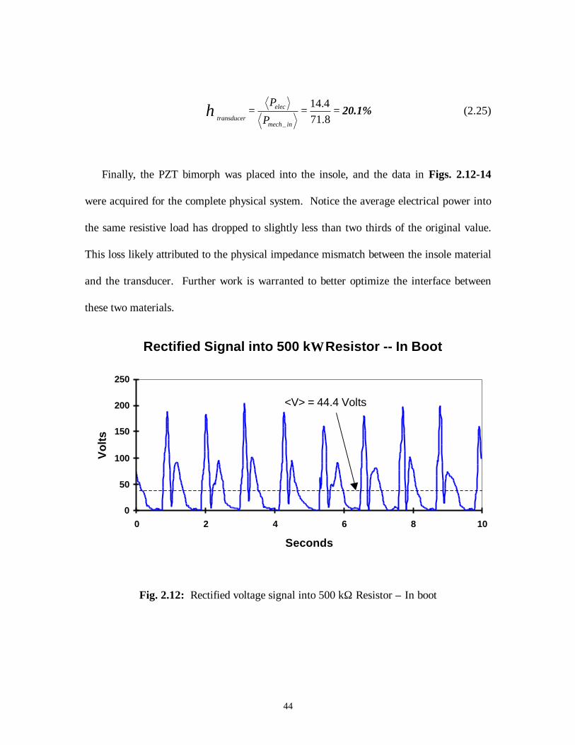
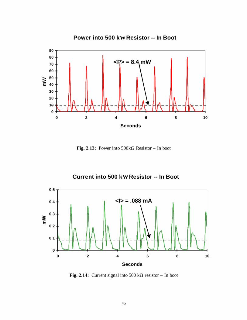
Finally, the PZT bimorph was placed into the insole, and the data in Figs. 2.12-14
were acquired for the complete physical system. Notice the average electrical power into
the same resistive load has dropped to slightly less than two thirds of the original value.
This loss likely attributed to the physical impedance mismatch between the insole material
and the transducer. Further work is warranted to better optimize the interface between
these two materials.
Rectified Signal into 500 kΩ Resistor -- In Boot
0
50
100
150
200
250
0 2 4 6 8 10
Seconds
Vol
ts
<V> = 44.4 Volts
Fig. 2.12: Rectified voltage signal into 500 kΩ Resistor – In boot
45
Power into 500 kΩ Resistor -- In Boot
0
10
20
30
40
50
60
70
80
90
0 2 4 6 8 10
Seconds
mW
<P> = 8.4 mW
Fig. 2.13: Power into 500kΩ Resistor – In boot
Current into 500 kΩ Resistor -- In Boot
0
0.1
0.2
0.3
0.4
0.5
0 2 4 6 8 10
Seconds
mW
<I> = .088 mA
Fig. 2.14: Current signal into 500 kΩ resistor – In boot

46
From the previous graphs, the electromechanical efficiency of the complete system is
determined.
11.7%===8.714.8
__
inmech
elec
systphys P
Pη (2.26)
The result in Eqn. 2.26 is important for comparison against other shoe-mounted,
energy harvesting mechanical devices. The real metric is the electrical efficiency of the
conditioning electronics developed herein which make this source useful. These will be
developed in the following three chapters.

47
Chapter 3
Selection of a Power Conditioning Topology
This chapter discusses the selection of a power conditioning topology given the bimorph
source characteristics derived in the previous chapter. It begins by enumerating the
electrical constraints imposed upon the system and further compares three conditioning
schemes. The first of these termed “direct-discharge” throughout this report, was used by
the MIT Media Laboratory in their previous design. The other two approaches are high-
frequency switching converter topologies -- the buck converter and its isolated
counterpart, the forward converter. A brief overview of high-frequency dc/dc switching
converter theory and a discussion of commercial, off-the-shelf switch controllers are
provided. Finally, system layouts for both the buck and forward converters are presented
for comparison of performance.
3.1 Electrical Constraints
By examining the equivalent circuit (Fig. 2.9) and in-boot signal plots (Figs. 2.12-14)
presented in the previous chapter, it is seen that the PZT bimorph has poor source
characteristics which create a few issues when efficient conversion schemes are compared.
The bimorph source is essentially purely capacitive (~140 nF) and produces high-voltage,
low-energy, low duty-cycle current pulses at an average frequency of approximately one

48
cycle per second when excited by walking. All of these characteristics lead to an
extremely high impedance and difficult to regulated micro-power source.
Because excitation occurs at such a low frequency, and it is desirable to provide a
constant, low-ripple output voltage, the power conditioning system must perform a low-
pass filtering operation with a significantly low corner frequency. With the previous goal
in mind, the most efficient technique would be to discharge the source through a diode and
an inductor into a “bucket” capacitor. The load network is matched to the capacitance of
the source at the frequency of excitation, and the network is rung with each step, thereby
charging the bucket capacitor. Similar techniques are often used in ac charging circuits for
capacitors in flash photography systems[20]. At an average one Hertz walking pace and
with a capacitive source measuring 140 nF, however, this technique would call for an
inductance on the order of 200,000 H. Certainly, such a value is not practical, especially if
one expects the device to fit in a shoe. The goal of power conditioning could therefore be
restated as efficient energy transfer from a high-voltage, “small” capacitor to a low-
voltage, “large” bucket capacitor.
This chapter explores three approaches to accomplishing this objective. The first, the
direct-discharge method, ignores the need for an impedance match between source and
bucket capacitors. With each pulse from the bimorph source, charge is leaked through a
diode bridge directly into the bucket capacitor. The second two methods high-frequency
switching techniques which effectively induce a charge gain and drive down the inductance
required to match the source with a load. Moreover, all three methods discussed herein

49
will require some amount of output stage linear regulation, so this topic is not addressed
specifically in the comparison. The average input/output voltage difference of such
regulation is important and will vary from method to method; however, this value is a
function of the ripple ratio, not the regulator or the architecture selected.
3.2 Direct-Discharge Method
Direct-discharge is modeled by the following equivalent circuit:
Cb
(Piezoelectric Source)
vl(t)
2Vdd
-+
~qp(t) +
-
ip(t) il(t)
Cp rl(t)
ic(t) id(t)
Rd
ib(t)
vs(t)
+
-
Fig. 3.1: Equivalent circuit for the “direct-discharge” architecture
The bimorph source model derived in the previous chapter is connected in parallel to the
bucket capacitor Cb and a variable resistor Rl. When the output regulator stage of such a
system is turned OFF, Rl represents only the leakage current through the dielectric of Cb
and the quiescent current of the regulator and load stage. When the load is ON, however,
Rl depends upon the impedance of the load and the loss in the regulator. Finally, the
voltage source “2Vdd” models the diode drops experienced through a diode bridge
rectifier.

50
Typically, a circuit like the previous would require a number of current pulses from the
source to charge Cb at start-up before the load stage is turned ON and Rl begins to draw a
significant amount of current. Once a specified threshold is reached for the voltage Vl, the
load stage is activated and Cb begins to discharge assuming the current required by Rl is
greater than that provided by the source. Similar to the previous Media Laboratory
design, Cb is allowed to discharge to specified voltage, and the cycle repeats.
There are a few important aspects of this conditioning scheme which demand
attention:
• Energy is transferred from the source capacitor to Cb only after Vs(t) has reachedthe sum of the load voltage Vl(t) and 2Vdd and after the diode bridge begins toconduct.
• With each current pulse from the source capacitor Cp, the voltage across thecapacitor will rise quickly to the sum of Vl(t) and 2Vdd, and remain there for theremainder of the current pulse.
• Because the relationship Q=CV holds for both source and bucket capacitors, Q isfixed for each current pulse and the ratio between Cb and Cp is necessarily high(Cb/Cp = ~103), the voltage across Cb rises (over the same period) at onethousandth of the rate at which the voltage across Cp would have risen were it notloaded.
These observations lead to a general conclusion that the direct-discharge method
clamps the source voltage quite low in comparison to the natural tendency of a
piezoelectric source. Now, given that the energy delivered to Cb during each current
pulse is Q⋅Vl, and the total charge Q liberated during each current pulse is fixed and
relatively constant, clamping the voltage is equivalent to clamping the energy over a cycle,

51
or the power, transferred to the load stage. This result is the classic first-year electrical
engineering problem concerning the energy that “disappears” when transferring charge
between capacitors of widely disparate values. Even if the capacitors perfectly matched,
only one quarter of the original energy can be transferred from one capacitor to another,
and half of the total energy lost, if no other energy storage elements are placed in between.
Moreover, the most efficient way to transfer energy off of a charging capacitor is by
allowing it reach a maximum voltage and then leak off the charge through an exponential
voltage decay. That is what happens during an RC decay and, in a sense, is why
supplementing a capacitive load with a matched inductance is advantageous in ac systems.
To further illustrate this point and to quantify the inefficiency of such a system, the
following mathematical model is derived. Using the equivalent circuit in Fig 3.1, and
assuming an average load voltage <Vl> over the charge/discharge cycle,
(3.1)
where
voltage ON Diode Vtime on-turn Diode
voltage Load
ecapacitanc Sourceresistance equivalent leakage Dielectric
current sourceCharge
voltage Source
dd ==
===
==
d
l
p
d
q
p
t)t(v
CR
I
)t(v
ll
dCRt
dqp
V)t(v
tt0e1RI)t(v pd
=
<≤
−=
−

52
and td is the solution of
(3.2)
The previous equations describe the source and load voltages during the brief period
before the rectifier diodes turn ON. From the results of Sect. 2.4, the charge source is
assumed to ramp linearly with each footfall and subsequent heel lift, thereby providing an
approximately square pulse of current to Cp and Rd. The magnitude of this pulse is Iq,
which has length a and period T in the following derivation. The next series of equations
result in a function describing load voltage vl throughout a current pulse cycle.
(3.3)
where
ecapacitanc Bucket resistance Load
==
b
l
CR
Now, in the Laplace domain,
(3.4)
−=+
−
pdCRt
dq e1RIVlVdd2
0
( ) ( )
I Cdvdt R
v C dvdt R
v
Cd v V
dt Rv V C
dvdt R
v
q pp
dp b
l
ll
pl dd
dl dd b
l
ll
= + + +
= + + + + +
1 1
2 12
1
( )( )Is
C C sV vR R
V VsR
qp b
ll l
d ll
dd
d
= + − + +
+1 1 2

53
solving for Vl, and letting Ce = Cp + Cb and Re = Rd||Rl,
(3.5)
or,
(3.6)
At the end of the current pulse, the charge across Cp is nearly drained, so it is assumed
that negligible charge leaks through the diodes and onto the bucket capacitor after t = a.
Moreover, the voltage vl(t) begins to decay though Rl, or
(3.7)
where
(3.8)
and
(3.9)
Now, the energy transferred to the load is found using the following equation:
V
IC
VR C
s v
s sR C
l
q
e
dd
d el
e e
=− +
+
2
1
v t I R VRR
e v e t t al q e dde
d
t tR C
l
t tR C
d
d
e e
d
e e( ) = −
−
+ ≤ <
− − − −
2 1
v a I R V RR
e v el q e dde
d
a tR C
l
a tR C
d
e e
d
e e( ) = −
−
+
− − − −
2 1
v t v a e a t bl l
t aR Cbl( ) ( )= ≤ <
− −
v bl ( ) = 0

54
(3.10)
or
(3.11)
And, integrating the previous expression,
( )( ) ( )
( ) ( )
( )
( )
−
+
−
+
−−
−
−+
−+
−−−
−=
−−
−−
−−−−
−−−−
bl
ee
d
ee
d
ee
d
ee
d
ee
d
CRaT
bl
l
CRta
eel
l
CRta
eeCRta
eed
eddeql
l
CRta
eeCRta
eedd
eddeq
lt
eCR
avR
eCRvR
eCR
eCRRR
VRIvR
eCReCRtaRRVRI
RE
22
22
2
22
12
)(1
12
1
12
122
12
1221
(3.12)
From the previous equation, a three-dimensional plot of the theoretical energy
delivered to the load by a single current pulse over the variables Cb and Rl is developed.
The parameters <Vl>, Vdd, Cp, Rd, Qt, a and T are determined through experiment and
by observation of the signal produced by the bimorph insert at an average .91 Hertz
walking pace. Specifically:
( )E p t dtR
v t dl l
T
ll
T= =∫ ∫( ) ( )
0 0
21
I R V RR
e v e dt v a e dtq e dde
d
t tR C
l
t tR C
l
t aR Cb
a
T
t
ad
e e
d
e e l
d
−
−
+
+
− − − − − −
∫∫ERl
l
=
12 1
2 2
( )

55
• <Vl> = 9.7 V; the average voltage across C1 in the Media Laboratory design• 2Vdd = .6 V; two times the voltage drop across the diodes chosen herein• Cp = 143 nF; measured capacitance of the bimorph device• Rd = 10^7 Ω ; approximate value for dielectric leakage equivalent resistor,
determined from unloaded exponential decay plots of bimorph• Qt = 4.4e-5 C; determined from average current into the highest-yield load at a
given frequency, or
( ) C/pulse seck V 5
pulsel
lt 104.455.
5004.44
TRV
Q −×=
Ω=⋅
= (3.13)
• a = .075 sec; by inspection of signal plots (average)• T = .55 sec; average period between pulses
A Matlab™ script was developed to produce the following meshed plots. (See
Appendix B.) The first plot shows the energy delivered to a load at start-up, that is, with
no initial load voltage (<Vl> = 0 V). The second uses the initial <Vl> value given above.
Fig. 3.2: Energy delivered into various loads via direct-discharge (<Vl>=0V)
mJ

56
Fig. 3.3: Energy delivered into various loads via direct-discharge (<Vl>=9.7V)
It is apparent from Figs. 3.2 and 3.3 that the energy transfer characteristics at start up
are nearly the same as when the load stage is supporting a relatively small average voltage.
The saddle in the “low-Rl, high-Cb” region of the second plot is a result of the energy
already stored in the load at the beginning of the current pulse; the reader should therefore
not interpret that region of the graph to signify a promising load combination. Examining
the preceding zero voltage graph reveals that the energy transfer at start-up into that
magnitude of Cb is quite poor and would require many more current pulses to bring the
average load voltage <vl> up to nearly ten Volts. In addition to the previous plots, the
maximum energy transfer via direct-discharge was calculated using the given parameters.
In both cases, the peak energy into the load reaches a maximum of 2.5 mJ when Cb is
smaller than 10 nF, and Rl is approximately 320kΩ . In contrast, the energy stored on the
mJ

57
source capacitance is found to reach 6.8 mJ if it were it not discharged over the length of
the pulse (i.e. through an exponential decay). This point reinforces the advantage of
removing the source energy when the voltage reaches its peak.
While direct-discharge appears to be nearly 37% efficient at the best matched load,
that is only true over a limited and undesirable range of loads. From Eqn. 3.12, a quick
calculation reveals that the longest time constant among any load combinations which
draw at least .5 mJ of energy is about 1.78 seconds. This time constant translates into an
output voltage ripple of one quarter the value of the average output voltage <vl>, and a
transfer efficiency of approximately 7.4%. Using specific Rl and Cb values taken from the
simulation output,
( )( ) 78.11010 725.7 ==≅ −blCRT (3.14)
and
% Ripple TC 27e1100e1100 78.155.T
=
−×=
−×=
−
−
(3.15)
with
% EE
max
out 4.78.6
5. ===η (3.16)
This ripple voltage ratio is significant and will further contribute to load stage loss via the
equivalent series resistance of the filter capacitor and, principally, the voltage drop-out

58
through the regulator. Finally, the ripple ratio becomes completely unreasonable ( > 60%)
as component values approach those which yield only 1 mJ per cycle.
In summary, the direct–discharge architecture is a viable but inefficient approach to
conditioning the energy liberated by a piezoceramic shoe insert. It was found that, even
with most well-matched load, the energy transferred to the load is approximately one third
of that available from the source. Moreover, choosing load components to reduce output
voltage ripple further reduces transfer efficiency. These results reinforce a few of the
points made at the beginning of this section. Particularly, it is advantageous 1) allow the
source voltage to peak (into the 100’s of Volts, in the case of the bimorph source) before
loading it, and 2) to not directly load a low-frequency piezoelectric source with a large
capacitor that will clamp its voltage. The following section presents high-frequency
switching techniques better suited to address these concerns.
3.3 Overview of Switching Converters and Topology Selection
High-frequency switching converters are power conditioning circuits whose
semiconductor devices operate at a frequency that is “fast compared to the variation of
input and output waveforms[21].” They are used most often over linear regulators as a
more efficient interface between dc systems operating at disparate voltage level, and are
the work horse of computer and consumer electronic power supply circuitry today. The
following paragraphs provide a brief overview of the theory behind high-frequency
switching converters and the reasoning behind their selection in this application.

59
Switching power supplies offer two distinct advantages over linear voltage regulators.
Primarily, because they are truly power converters and not simply voltage regulators,
switching converters are quite efficient even when the difference between input and output
voltages is large. On the other hand, the average values of the input and output currents
in a linear regulator must be the same. Therefore, the power lost through a linear
regulator is the product of the input current with the difference between the input and
regulated output voltages. Because piezoelectric voltage signals typically have a relatively
large domain, and it is disadvantageous to clamp this signal, linear regulators encounter
some obvious drawbacks which switching converters are well-suited to meet.
In a sense, a linear regulator is an active resistive divider in series with the load. They
regulate the output voltage by dissipating excess power for given input current. In stark
contrast, switching converters conserve input to output power (less overhead power),
regulating either voltage or current at the output stage. They can be thought of as
“impedance converters” becuase the average dc output current can be smaller or larger
(step-up or step-down, respectively) than the average dc input current[22]. This impedance
conversion property is the second notable advantage to using a switching converter over a
linear regulator with direct-discharge because of the large impedance mismatch inherent in
this design.
Discussion of high-frequency switching converters is best framed by defining a two
port device into which the power flow between ports is conserved but the average
voltages and currents at either end are controllable. This two port device has a series and
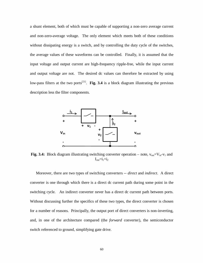
60
a shunt element, both of which must be capable of supporting a non-zero average current
and non-zero-average voltage. The only element which meets both of these conditions
without dissipating energy is a switch, and by controlling the duty cycle of the switches,
the average values of these waveforms can be controlled. Finally, it is assumed that the
input voltage and output current are high-frequency ripple-free, while the input current
and output voltage are not. The desired dc values can therefore be extracted by using
low-pass filters at the two ports[21]. Fig. 3.4 is a block diagram illustrating the previous
description less the filter components.
Vin vout
+ +
- -
+ v1 -
v2
+
-
i1 Iout
i2
Fig. 3.4: Block diagram illustrating switching converter operation – note, vout=Vin-v1 andIout=i1+i2
Moreover, there are two types of switching converters -- direct and indirect. A direct
converter is one through which there is a direct dc current path during some point in the
switching cycle. An indirect converter never has a direct dc current path between ports.
Without discussing further the specifics of these two types, the direct converter is chosen
for a number of reasons. Principally, the output port of direct converters is non-inverting,
and, in one of the architecture compared (the forward converter), the semiconductor
switch referenced to ground, simplifying gate drive.

61
The conversion ratio for a direct converter depends completely upon the duty-cycles
of the switches, which operate synchronously and out of phase. Simply, the duty-cycle D
is defined as the percentage of the switch cycle during which the direct current path is
closed. By applying the constraints that an inductor cannot support an average voltage,
and a capacitor cannot support and average current, one finds[23].
DVVDVvV xz =⇒==
1
212 (3.17)
and,
DIIDIiI xy
1
1
221
−=⇒−== (3.18)
Fig. 3.5 is a common switch architecture for the buck converter, the first of two
specific architectures considered and an appropriate staring point for discussing direct
high-frequency switching converters.
V1 V2
+ +
- -
I1 I2
C
L
zl(t)
Fig. 3.5: Switch implementation in the direct down (or buck) converter with load

62
During the early stages of the development process it was anticipated that the power
conditioning electronics proposed for the PZT bimorph would be controlled using an off-
the-shelf IC controller. Maxim, Inc., Linear Technologies, Inc., and others have a large
assortment of such devices available, many of which designed for low- and micro-power
applications. In fact, one of these controllers was seriously considered for the design
proposed herein. For a number of reasons, however, it was determined that such a device
is unsuitable for this application. Simply, they are designed for low-voltage conversion
and regulation of a dc voltage source – not at all similar to this application – and their
adaptation offered no real advantage over a new design.
All of the low-power switch control ICs considered were 1) limited in input voltage up
to approximately 18 Volts, 2) optimized for input currents greater than 1 mA, and 3) used
current-mode controller schemes requiring a feedback signal. Because of the desire to
maximize source voltage before loading the transducer, all ICs with an internal switch
were ruled out because none are capable of supporting the high voltages encountered with
the bimorph source. Those which require external FET switches on the other hand leave
the designer more freedom. That room often comes with the price of higher quiescent and
operating current requirements, however, and these ICs are still limited into the 10s of
Volts. Finally, the bimorph source is incapable of directly supplying the current required
by the IC – there is enough power, but the source impedance is much to high to supply
appreciable current. This problem is one that must be addressed by any design
implementing a switching converter. In Chapter 2 it was shown that the average current
developed by the bimorph source into a well-matched load was .088 mA, not nearly

63
enough to operate any reasonably high-frequency oscillator. These conditions point to the
need to bootstrap the system at start-up and draw subsequent current for the conditioning
electronics from the output side of the switcher.
With bootstrapping and supply feedback, use of an off-the-shelf IC is feasible for
implementing a direct down converter in this design. This practice is relatively common in
systems (such as off-line ac power converters) where the input voltage is unacceptably
high to source the conditioning electronics directly. There are some specific aspects of the
bimorph source signal which make IC controllers undesirable still. Switch control ICs are
designed to regulate voltage as well as convert power; however, voltage regulation is not
a concern for the switcher in this design. The purpose of the switching converter
proposed herein is to perform an impedance match between disparate capacitive networks.
All charge on the source should be removed quickly at the conclusion of each current
pulse – if not, it is lost when the signal inverts. Therefore, any desire to regulate the
output voltage by adjusting the duty-cycle of the switcher is a moot concern -- a relatively
large output ripple is to be expected and is unavoidable. The converter must simply
switch an exponentially decaying envelope at a high enough rate so as not to saturate the
inductor. Furthermore, unlike in the direct-discharge methods, properly matching to the
load resistance is not a concern. The energy transfer will be the same in any case – only
the RC time constant of this decay envelope will change.
In summary, an intricate switch control scheme is unnecessary and undesirable. Most
of these schemes observe the output voltage or current signal level and adjust the duty-

64
cycle accordingly. Where a large output ripple voltage is expected, it becomes more
important to observe the input waveform in this design, turn ON the switcher near its
peak, and turn it OFF when the charge has been drained. Because commercial ICs strictly
perform output waveform switch control, they are eliminated from discussion altogether.
If a means were developed to adapt off-the-shelf ICs in such a way to perform the control
desired here, they would probably be more efficient than anything constructed from
discrete parts.
In the spirit of simplicity, switch duty-cycle is kept constant in the following design.
Because this design is concerned principally with matching the impedance of dissimilar
capacitors and output regulation is not the goal for the switcher, strict duty-cycle control
is not a concern, and simple ON/OFF control of the switcher is performed. As previously
shown, low-frequency ripple is unavoidable using a realistically sized output filter.
Moreover, where load impedance is dominated by a large bucket capacitor, one can
consider the load/source impedance ratio to be fixed. Setting a constant duty-cycle is
therefore appropriate. Following from Eqn. 3.17 and 3.18, the impedance matching
property for the buck converter is shown to be related to the square of the duty-cycle.
2
1
11
1
1
2
2 DIV
DIDV
IV ==− −
or
12
2 ZDZ = (3.19)

65
In words, when the switch is ON, current through inductor ramps up linearly with a
slope proportional to the voltage drop across the inductor -- in this case the difference
between the source voltage and the voltage stored on Cb. After the relatively brief ON
time, the switch is turned OFF, the bimorph charge source is unloaded, and the current in
the inductor ramps down from its peak value with a slope determined by the voltage on
Cb. Where the voltage on Cb is much smaller than the source voltage (which in this
design it certainly is), a “charge gain” is introduced – less charge is removed from the
source capacitor than is delivered to the bucket capacitor because the inductor current
continues to flow even after the switch is turned OFF. This charge gain is proportional to
the inverse of D2 as shown in the previous equation. Recalling that the bimorph insert is a
fixed charge source, thinking of switching converters as a means by which to implement a
charge gain is a helpful mnemonic for understanding how the source power is conditioned
in this design.
With switch duty-cycle fixed, the output stage signal will mirror the voltage decay
envelope of the input stage when the switcher is activated. Further, the ratio between the
voltage level at input and output will be set by Eqn 3.16 and the current will likewise be
set by Eqn. 3.17. Bearing in mind that the unloaded source voltage is often 250 Volts or
higher, the previous points imply that the buck converter switch duty-cycle will have to be
quite small (~ 1/20 or .5%) so that the average of the voltage decay signal on the output
side is within the desired range (typically 3-5 Volts for battery operated devices) and the
inductor core does not saturate when the source voltage is high. Further, in this duty-
cycle range, switch stresses and losses associated with switch speed could be quite high.

66
It is generally most desirable to operate at a duty cycle close to 50%[21]. Most significant
to this design, however, is that the gate drive circuitry for the buck converter is necessarily
more complicated and lossy because the high-voltage side of its gate must be referenced to
the source signal.
By adding a step-down transformer to the buck converter topology, the forward
converter is created, and the component stresses problems associated with widely
disparate input and output signal amplitudes are reduced. Further, because impedance
reflected through a transformer is related to the square of the turns ratio N, the charge
gain becomes the product of N2 and D2 in the forward converter[24]. This advantage
provides for a switch duty-cycle closer to 50%, and a softens the requirements on
switching speed. Finally, gate drive circuitry in the forward converter is simplified because
the load stage is isolated, allowing the semiconductor switch to be referenced to ground.
These advantages, however, do not come without commensurate disadvantages.
Because the transformer steps-down the voltage to the output stage and energy is only
transferred from the source when the inductor in the filter network has a forward voltage
drop (i.e. secondary voltage is greater than the voltage stored on Cb), the forward
converter topology will only transfer energy from the source capacitor when the source
voltage is greater than the product of Vl and N. Therefore, as N increases, the source
voltage below which energy cannot be transferred from the source also increases. Power
losses in the winding resistance and the transformer core will further compound this
problem.
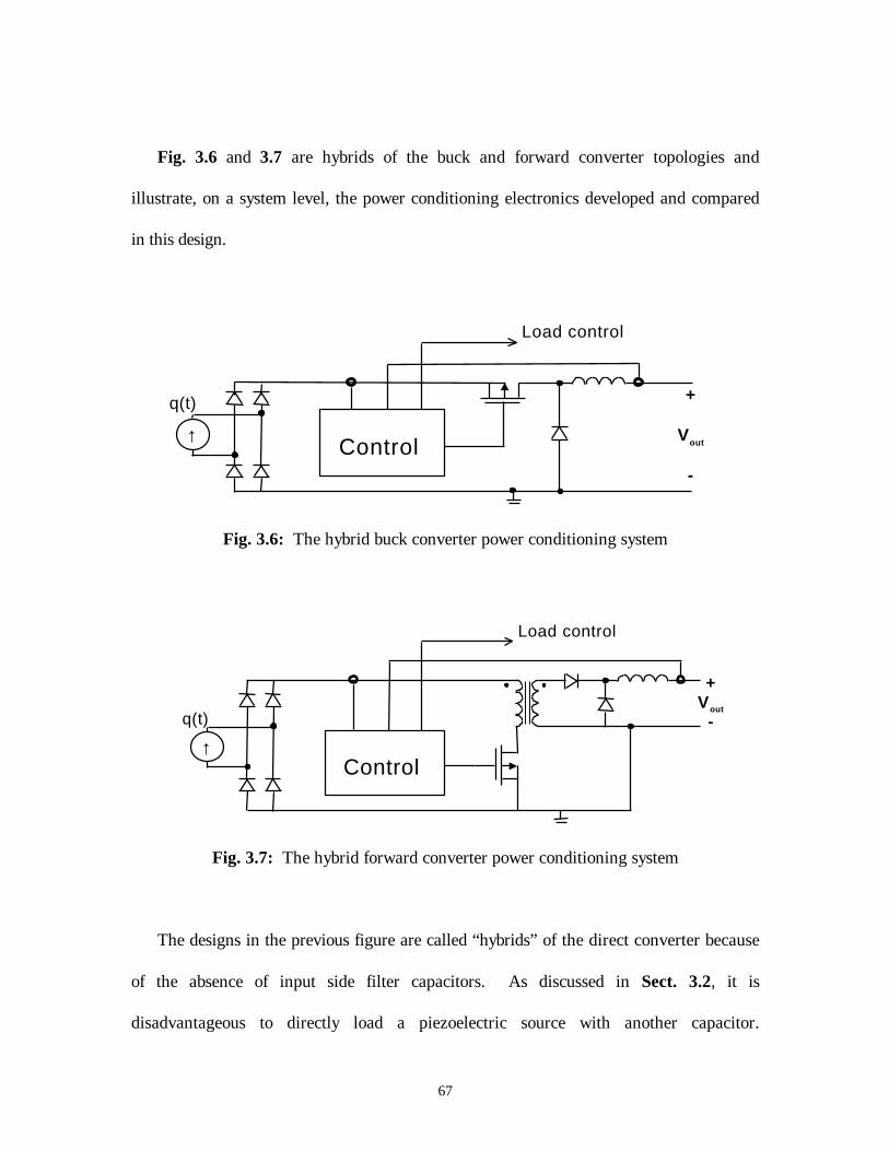
67
Fig. 3.6 and 3.7 are hybrids of the buck and forward converter topologies and
illustrate, on a system level, the power conditioning electronics developed and compared
in this design.
+
Vout
-
q(t)
Load control
Control↑
Fig. 3.6: The hybrid buck converter power conditioning system
+Vout
-
Load control
Control
q(t)
↑
Fig. 3.7: The hybrid forward converter power conditioning system
The designs in the previous figure are called “hybrids” of the direct converter because
of the absence of input side filter capacitors. As discussed in Sect. 3.2, it is
disadvantageous to directly load a piezoelectric source with another capacitor.

68
Furthermore, the systems described is not truly a dc/dc converter at all. The input signal,
a periodic decaying current pulse, is decidedly ac. The control system illustrated must
only monitor the source voltage for its peak and operate the switcher at a constant duty-
cycle until all charge is removed. When the output voltage is in range, the control turns
the load ON allowing the output bucket capacitor to source current. The specifics of
system architectures and component selections are discussed in the following chapters.

69
Chapter 4
Power Conditioning System
The following sections provide a functional description of the power conditioning
electronics proposed herein. Discussion in this chapter does not concern specific
component values or the optimization of parameters, but rather gives the reasoning behind
the design at the systems and components level. It begins by listing the secondary
functions of and constraints on the control system and follows with a piecewise
description of the following stages: 1) input rectification and bootstrapping, 2) high-
frequency switching, timer biasing and control, 3) secondary-side filtering, load control
and ON/OFF switching.
4.1 Ancillary Requirements and Constraints
As previously discussed, the fundamental objective for the electronics design is to
efficiently transfer energy from the high impedance bimorph source to a relatively large
storage capacitor. This function requires high-frequency switching of a decaying voltage
envelope from the bimorph source after each signal peak. The switching converter
topologies discussed in Chapter 3, hybrids of the buck and forward converters, serve as
the framework for power conditioning system design. The control is essentially the same
for both topologies presented herein, with the exception of the gate drive circuitry. There
area a few ancillary issues, however, which must also be addressed in order implement
these topologies. These are:

70
• Sensing the primary-side voltage signal peak with minimal loss• Providing for a bootstrapped “cold” start-up• Minimizing switching loss by keeping oscillator ON/OFF duty cycle low• Controlling load regulation so that momentary over-current does not require a
subsequent cold start-up
First, to switch the most power from the source signal’s decaying envelope, it is
necessary to sense the source signal peak. The sensing impedance must be particularly
high because the source impedance is also quite high and the available power is relatively
low. In contrast, increasing the shunt impedance degrades the accuracy of the sensing
measurement because currents through the shunt approach levels at which gate charging
and leakage in the CMOS logic begin to have unpredictable effects. The wide disparity
between turn-on and turn-off voltage compounds this problem as input ratings on CMOS
comparators are normally limited to within a few tenths of a Volt above the supply
voltage. Therefore, one goal of this design is to develop a novel sensing technique that
either loads the source very briefly and only when necessary, or one which performs zero-
slope peak detection with an extremely large input impedance.
A second design concern is that the circuit must bootstrap itself from a cold start-up.
In commercial off-line converter designs it is typical to find start-up circuits which draw a
small amount of current directly from the source to charge a short-term storage
capacitor[22]. When the voltage across that capacitor reaches some threshold, the stored
charge is dumped into the regulation electronics providing a “kick start” for the converter.
This general scheme is applied here. Further, when dealing with micro-Watt control
power levels like those encountered in this design, it is particularly advantageous to reduce

71
the number of components added to the design for short-term functions like start-up and
turn them off after use. Therefore, a bootstrapping scheme that draws charge directly into
the bucket capacitor only during start-up is desired.
Thirdly, the primary loss mechanism of most micro-power, high-frequency switching
converters are the oscillator and any components exposed to the high-frequency switching
signal. In general, it is best to minimize the number of elements operating at higher
frequencies because CMOS gate losses are linearly related to the operating frequency[22].
Conversely, higher switching frequencies allow for the use of smaller electromagnetic
components (not including the bucket capacitor, in this case, as the operating cycle is so
large that a large output capacitance is necessary). In the forward converter, the design
trade-off is therefore to balance switching losses with transformer losses over frequency.
This optimization does not affect the system layout, however, and is thus saved for
Chapter 5. One additional loss consideration remains to turn the oscillator and biasing
circuitry OFF when not in use. This convention is quite common and would significantly
enhance system efficiency because the switching subsystem is the most power hungry.
Finally, one of the advantages of the forward converter over the buck is that the step-
down transformer bears the brunt of the voltage down conversion. The switch duty-cycle
thus remains near 50%, reducing switch speed (i.e. gate drive power) and energy storage
requirements. It is therefore important to find an efficient way to bias the ‘7555 CMOS
oscillator circuitry for a 50% switching duty-cycle.

72
Finally, assuming that the system has bootstrapped and is providing power through the
linear regulator, there should be a failsafe to prevent discharge of the bucket capacitor past
the point at which there is no longer enough energy stored in the system to run the control
circuitry. That is, the higher priority for stored energy lies with the controller, not the
load. This convention makes sense considering the relative inefficiency of and time
required for direct discharge-energy transfer (via the start-up feedforward loop) compared
to switched transfer. In a case of a sudden over-current to the load, the load will
experience a disruption in service whether the stored energy on Cb were completely
dissipated or just to a point at which the switcher could not longer function. The length of
this disruption should be made as large as possible, and avoiding the need for a less
efficient cold start-up after each over-current would do just that. This convention implies
turn-on/off thresholds on Cb for the output stage regulator. Finally, because the
unregulated voltage ripple will be relatively large (1-2 Volts), some ON/OFF hysteresis is
required for stable supply to the load.
In summary, four subsidiary requirements are demanded of this power conditioning
system to address the issues presented at the beginning of the section. These are:
1) A high-impedance, source voltage peak detection technique2) A bootstrapping scheme that minimizes component count by drawing start-up
charge directly into the secondary-side capacitive bucket3) Efficient biasing for a 50% duty-cycle control for the ‘7555 CMOS timer, with
sleep mode control4) Load ON/OFF switching with hysteresis

73
4.2 Electronic System Description
The proceeding sections discuss the three principal stages of the switch controller
designs for the buck and forward converters: 1) input rectification and bootstrapping
latch, 2) high-frequency switching, timer biasing and control, 3) secondary-side filtering,
load control and ON/OFF switching. All component names refer to Figs. 4.1a and 4.1b
on the following pages. They are essentially the same controller, with different switch
drives and output filtering and a step-down transformer in the forward topology. The
following discussions will therefore not duplicate development of the two control systems;
they will trace the systems jointly and highlight any differences between them.
4.2.1 Input rectification and bootstrapping latch
It is important to note from the outset that this electronics design has two ground busses –
one referenced to the bimorph source, the second referenced to the load. These ground
references will be referred to as “source ground” (SGND) and “load ground” (LGND)
respectively. The two busses are joined by an n-channel MOSFET Mg whose source is
connected to SGND and whose drain is connected to LGND. Because the bucket
capacitor Cb is sufficiently discharged and the zener diode Z2 is not conducting at start-
up, the gate of Mg is pulled to SGND by the R3. This configuration assures that SGND
and LGND are not referenced to each other at start-up, and will not become so until Q1
goes into conduction. This latching circuit is identical to the one used by the MIT Media
Laboratory in its earlier design, and it is recycled here for bootstrapping the system
described herein. (See Appendix A for a functional description of the latching circuit.)
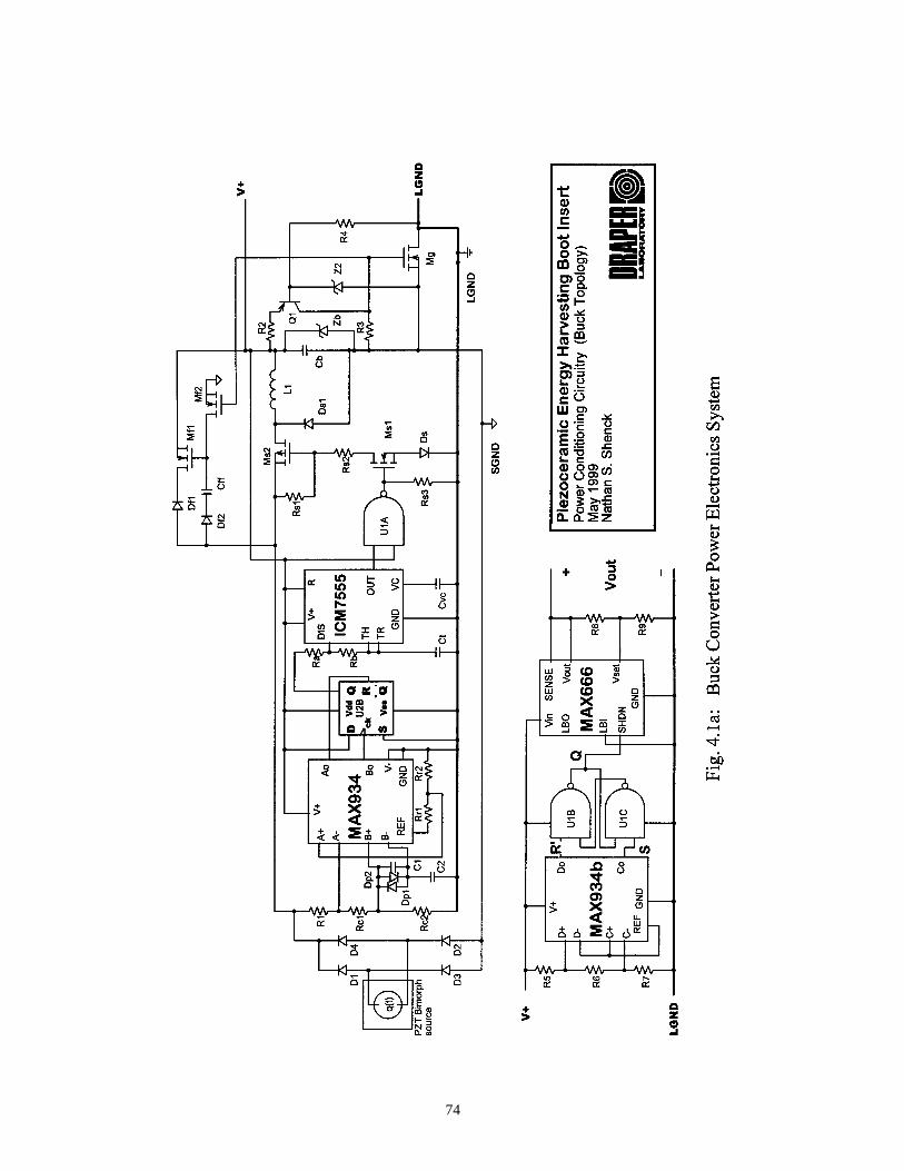
74
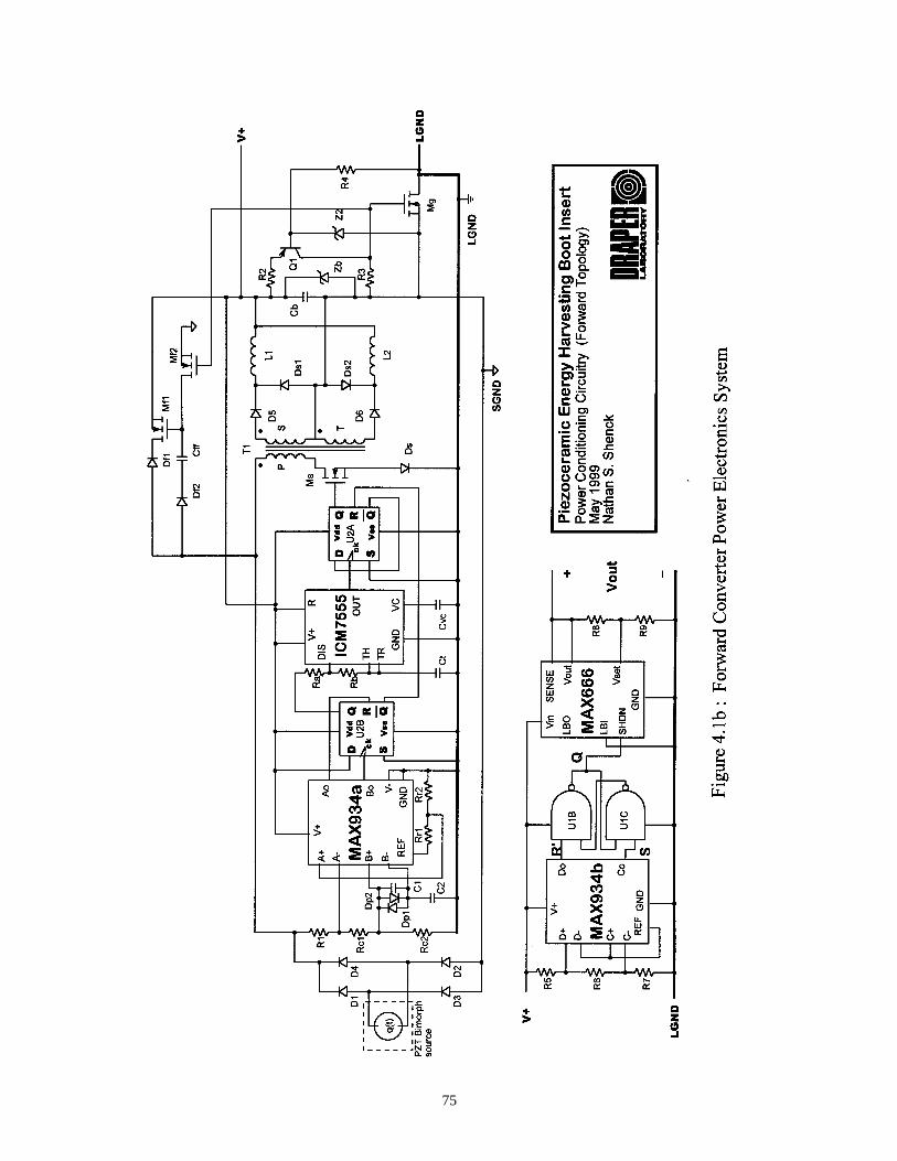
75

76
Following from left to right, the signal is first full-wave rectified through the diode
bridge (D1 – D4). Because LGND is not referenced to the source and Q1 is OFF at start-
up, the only current path available to the rectified source signal is through the feed-
forward loop along the top of the circuit diagram and into Cb. Diodes Df1, D5, D6, and
Ds1 (and Ds2) prevent the spontaneous discharge of Cb during the start-up process and
allow the voltage across it to ramp higher with each current pulse from the transducer. To
ensure that Mf1 is ON at start-up, Df2 and Cff are placed in series on a second
feedforward branch to couple charge onto its gate. Further, Mf2’s gate shares the same
node as the gate on Mg (i.e., they share the same conduction state assuming similar gate
thresholds), so Mf2 is OFF at start-up and charge is allowed to accumulate on Mf1,
holding it ON. It is important to note that both Mf1 and Mf2 must be low-leakage, high
stand-off voltage devices. It is desirable to minimize source charge leakage through Mf1
when it is turned OFF and the switcher is operating, and a leaky Mf2 would strip charge
off of the Mf1 gate during the start-up process.
As Cb charges beyond Z2’s breakdown voltage plus the “diode drop” across the base-
emitter junction of Q1, Q1 is forced into conduction, which in turn activates Mf2 and Mg.
With Mf2 on, Mf1’s gate is pulled to ground and current flow through the feed-forward
loop is blocked in both directions. Most high-standoff voltage MOSFETs have a body
diode connected from source to drain; however, Df1 prevents reverse current flow
through Mf1 despite that fact. Further, in the ON state, Mg references LGND to SGND,
which will then differ only by the voltage drop across the body of Mg. The high-side of

77
Cb now has a current path through the conditioning circuitry and into the “common”
ground, and the system is activated. Finally, LGND will remain a viable current return
path until the voltage across R3 goes low enough to pinch off Mg, and the value for the
voltage across Cb at which this load-switching occurs can be set by adjusting the ratio
between R2 and R3.
4.2.2 High-frequency switching, timer biasing and control
Once the control and regulation circuitry is activated and the direct current path from
the bimorph source to the secondary side is opened, the only means to transfer energy
from the source and into Cb is through the high-frequency switch. In the buck converter,
the switch Ms1 is open initially, holding Ms2 open as well, and the voltage across the
bimorph is therefore allowed to soar quickly upward as the bearer steps down or lifts the
heel. Similarly in the forward converter design, Ms is open at start-up, and the
transformer cannot transfer energy.
With the control circuitry activated, a D-type flip-flop, the Maxim MAX934™ and its
biasing circuitry perform zero-slope peak detection of the bimorph signal so that the
switcher is activated when the source signal reaches its maximum voltage. The MAX934
IC is a low-power quad comparator package. It was chosen for this design because of the
wide range in supply voltage (2.5 to 11 Volts), very low quiescent current (typically 5.5
µAmps) and convenient packaging of four comparators and a voltage reference[25]. R1,
Rc1, and Rc2 constitute a very high-resistance voltage divider (R1 ~ 100 MΩ ). Rr1 and

78
Rr2 divide down the reference voltage (1.182 Volts) so that the input voltage at pin A- is
limited to within the maximum rating as the source voltage approaches 300 Volts. Ao
therefore remains HIGH until the bimorph signal voltage reaches the determined level and
A- becomes greater than A+; the RESET pin on the flip-flop (U2B) is then set LOW. As
the input signal continues to rise, the voltage drop across Dp2 holds the B- pin higher than
B+, thereby holding Bo LOW as C2 charges.
When the slope of the source signal reaches zero and begins to fall, the voltage across
C2 is greater than the signal voltage and the voltage drop across Dp1 causes the
comparator to drive the Bo pin HIGH. With RESET LOW and a positive slope edge at
the clock input of U2B, the flip-flop latches Q high, thereby supplying power to the
biasing circuitry of the ICM7555™ oscillator. The oscillator will continue to operate as
long as Q is high and the biasing circuitry is powered. It will remain high until the input
signal falls below the threshold set at A+ and RESET is driven high. Further, feeding Ao
into RESET prevents the oscillator from being turned ON until the A+ threshold is
reached regardless of the source signal. This convention prevents small signals, such as
the ones produced by weight shifts on the insole, from inadvertently activating the
switcher. Rc1, Rc2 and C1 filter and bias the signal into the B-/B+ peak detector. They
were determined by experimentation, and the circuit behaves somewhat erratically without
them. Finally, another simple, more robust zero-slope peak detector circuit was
considered for this design, but the circuit developed here functions adequately and
requires less components[26].

79
A second turn-on technique was also considered in this design – activate the
electronics after the input signal reaches a constant “trip voltage”. The advantages of such
a convention are its simplicity and predictability. Choosing a fixed trip voltage prevents
premature triggers or activating the oscillator at low source voltages that require more
overhead power to switch than they provide to the load. Because the force of the footfall
is unique to each individual and different every time, the trip voltage for the switcher
would be set below the average peak voltage of the signal at each heel lift. The average
peak voltage of the heel lift would be used because it is typically 80 to 100 Volts smaller
than that of the heel strike. This trade off begs an optimization between energy transferred
and average “missed trigger” energy loss at each trip voltage; however, the force statistics
vary so much from person to person and activity to activity that the trip voltage could be
set after visual examination of some sample waveforms.
Once the trip voltage is determined, a means by which to sense the input signal passing
that threshold would be required. The high impedance shunt used in this design always
incurs some loss, even when the sum resistance is in the tens of megaohms; however, the
trip voltage convention makes another sensing approach feasible, one which loads the
source only briefly and without the difficulties posed by nanoampere order current
divisions. By shunting the input with a low-leakage zener diode, whose breakdown
voltage is set at the turn-on threshold, a current pulse can be delivered to a parallel RC
network every time the source signal passes the trip voltage. The high side of this
network could be tied to a CMOS buffer or comparator and used to turn ON the circuitry
for a length of time governed by the decay constant of the RC network and the LOW

80
signal threshold of the buffer. This optional circuit was constructed and provided reliable
performance.
Returning to the design herein considered, the outputs Q and Q’ of U2B have several
functions. Q is used to source current to the biasing resistors Ra and Rb during switch
operation in both converter systems. By using Q pin to source this current, quiescent loss
is reduced in the switching circuit by supplying power to the biasing resistors only when
the oscillator is needed. Moreover, Q’ is used to turn U2A OFF when the switcher is not
in use, opening the switch Ms. The three component biasing scheme used here (Ra, Rb
and Ct) is a common configuration for the ‘555 timer. It provides a voltage-invariant,
astable multivibrator with a controllable duty-cycle (between ~50% to 100%) and a
frequency range into the megahertz region. The ‘555 is chosen in this design for
numerous reasons: Its CMOS variants are common, have a wide input supply range, and
are most well suited to low-power oscillator designs requiring the degree of control
desired in this design[22]. Further, the simple biasing scheme make them easy to
implement. Without discussing the details, the following design equations govern its
operation[27]:
fRa Rb Ct
= +146
2.
( )(4.1)
and
DRb Ra
Ra Rb= +
+ 2 (4.2)

81
As previously discussed, the forward converter switcher will operate at or near to a
50% duty-cycle. This convention minimizes switch stresses and reduces transformer core
losses. By examining Eqn 4.2, it is observed, however, that the biasing convention
presented above is not capable of providing a strict 50% duty-cycle. Also, it will be
shown that biasing circuitry losses approach a maximum as duty-cycle go to 50%
boundary. The ‘555 timer operates by sensing the voltage levels at the trigger (TRIG) and
threshold (TH) pins. When the TH pin goes higher than 2/3Vcc, the output goes LOW and
the discharge (DIS) pin begins to sink current from the RC network into ground. As the
voltage on TRIG falls below 1/3Vcc, the output goes HIGH and the DIS pin is opened up
again beginning the cycle anew. The transition times between these thresholds are relate
to the different RC time constants for the two stages of the cycle and are given by
46.1)RbRa(Ct
THIGH
+= (4.3)
and
46.1CtRb
TLOW = (4.4)
Now, to find the total energy dissipated through the network during a cycle, the energy
required to charge Ct (through Ra and Rb) from 1/3Vcc to 2/3Vcc, or
( )( )
∫
+
+−
⋅−−
+=
46.1)RbRbCt
0
2
RbRaCtt
HIGH dteVcc32
VccVccRbRa
1E (4.5)

82
is summed with the energy dissipated through Rb when the DIS pin goes to ground, or
46.1CtRb
RaVcc
E2
LOW = (4.6)
By performing the integration, summing and combining terms, the equation for total
energy lost per cycle becomes
46.1VccCt
46.1VccCt
E22
CYCLE⋅+⋅= (4.7)
or, at the given switching frequency,
( )
+⋅=
RaRb
46.11
61
VccCtfP 2BIASING (4.8)
Eqn 4.8 reveals that the power lost through the biasing circuitry is not only dependent
upon the frequency and the square of the source voltage, but also depends heavily upon
the ratio between Rb and Ra. Moreover, when this equation is compared with the
relationship governing duty-cycle given in Eqn 4.2 one notices that it is impossible to
minimize the Rb/Ra ratio and approach a 50% duty-cycle – they are mutually exclusive
objectives.
To address this quandary in the forward converter system, another D-type flip-flop,
U2A, is used to establish a perfect 50% duty-cycle square wave at the Q output by feeding

83
its Q’ back to the DATA pin and clocking the flip-flop with the ‘555 timer circuit. The
output Q of U2A is used to drive the gate of the n-channel MOSFET switch Ms, whose
drain is connected to the non-dotted terminal of the primary of transformer T1 and whose
source is tied to LGND. Further, by tying U2A’s SET pin to ground and RESET to Q’ on
U2B, Ms is held open when the timer is not operating. Finally, both the ‘555 timer and the
flip-flop pair are referenced to LGND and supplied by a feedback loop from the secondary
side of the transformer.
There is one obvious drawback to using a flip-flop to ensure a 50% duty-cycle on the
switch. The square output Q will operate at one half of the frequency of the clock input.
This point brings into question the use of a flip-flop for duty-cycle stability in the forward
converter system. After quick examination of Eqn 4.8 (and respecting the realistic limits
of this ratio), however, the merits of this configuration are easily shown. Because of its
linear relationship to the operating frequency, power doubles when the frequency of the
timer is doubled. But, simultaneously reducing the Rb/Ra ratio by slightly more than one
half has an equal and opposite effect on power loss. Further, it can be shown analytically
that the gains made by lowering the Rb/Ra well outweigh the higher power associated
with operating the ‘555 timer at twice the frequency. Input power data has been collected
for the Maxim ICM7555™ timer IC operating through a range of frequencies. This data
is combined with the theoretical power loss calculated in Eqn 4.8 for the biasing circuitry
at different duty-cycles and frequencies. Further, it was confirmed experimentally that
duty-cycles as high as 99.5% or greater (through 200 kHz) have positive-going edges
resolute enough to trigger the clock of the 4000B-series CMOS, D-type flip-flops chosen

84
here. The results of this comparison are displayed in Figs. 4.2 and 4.3 and in Tables 4.1
and 4.2.
Note that the recommended minimum resistance value used to bias the ‘555 in this
configuration is 1 kΩ , and the maximum recommended sum of the two resistors is 3.3
MΩ . Also, the smallest recommended capacitance for Ct is .50 nF. The resistance
recommendations were followed in setting limits for the following theoretical calculations;
in contrast, the capacitance value was found to be more flexible in practice, and 47 pF was
chosen. Finally, Vcc was set to 4 Volts for all calculations.
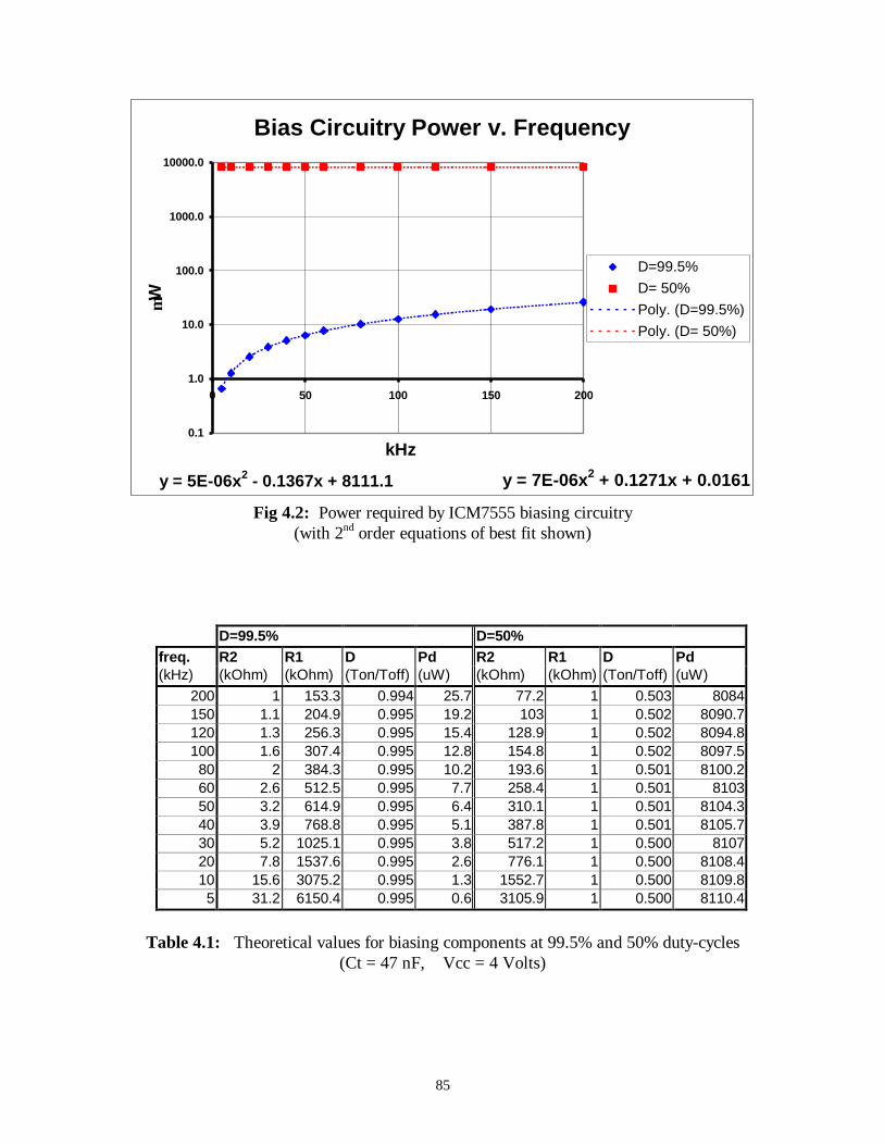
85
Fig 4.2: Power required by ICM7555 biasing circuitry(with 2nd order equations of best fit shown)
D=99.5% D=50%freq. R2 R1 D Pd R2 R1 D Pd(kHz) (kOhm) (kOhm) (Ton/Toff) (uW) (kOhm) (kOhm) (Ton/Toff) (uW)
200 1 153.3 0.994 25.7 77.2 1 0.503 8084150 1.1 204.9 0.995 19.2 103 1 0.502 8090.7120 1.3 256.3 0.995 15.4 128.9 1 0.502 8094.8100 1.6 307.4 0.995 12.8 154.8 1 0.502 8097.580 2 384.3 0.995 10.2 193.6 1 0.501 8100.260 2.6 512.5 0.995 7.7 258.4 1 0.501 810350 3.2 614.9 0.995 6.4 310.1 1 0.501 8104.340 3.9 768.8 0.995 5.1 387.8 1 0.501 8105.730 5.2 1025.1 0.995 3.8 517.2 1 0.500 810720 7.8 1537.6 0.995 2.6 776.1 1 0.500 8108.410 15.6 3075.2 0.995 1.3 1552.7 1 0.500 8109.85 31.2 6150.4 0.995 0.6 3105.9 1 0.500 8110.4
Table 4.1: Theoretical values for biasing components at 99.5% and 50% duty-cycles(Ct = 47 nF, Vcc = 4 Volts)
Bias Circuitry Power v. Frequency
y = 7E-06x2 + 0.1271x + 0.0161y = 5E-06x2 - 0.1367x + 8111.1
0.1
1.0
10.0
100.0
1000.0
10000.0
0 50 100 150 200
kHz
µW
D=99.5%D= 50%Poly. (D=99.5%)Poly. (D= 50%)
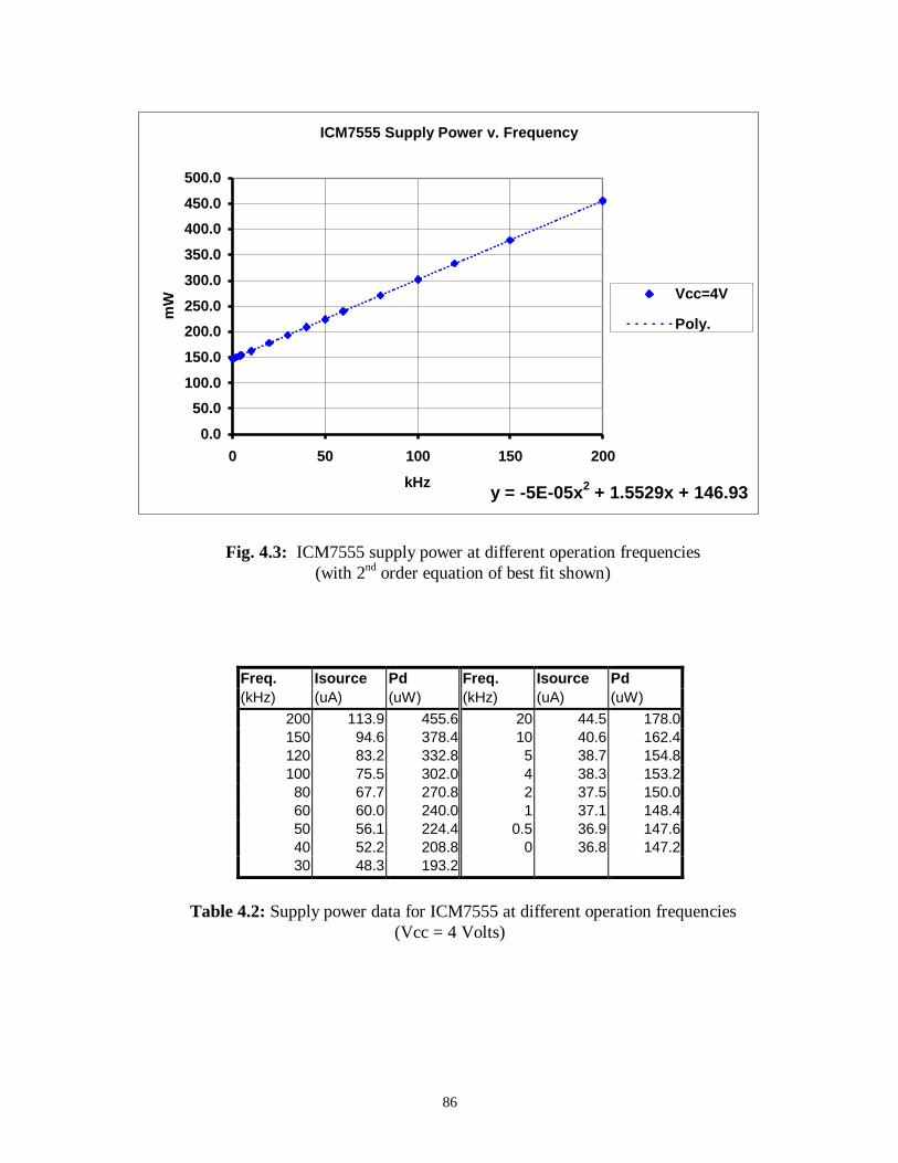
86
Fig. 4.3: ICM7555 supply power at different operation frequencies(with 2nd order equation of best fit shown)
Freq. Isource Pd Freq. Isource Pd(kHz) (uA) (uW) (kHz) (uA) (uW)
200 113.9 455.6 20 44.5 178.0150 94.6 378.4 10 40.6 162.4120 83.2 332.8 5 38.7 154.8100 75.5 302.0 4 38.3 153.280 67.7 270.8 2 37.5 150.060 60.0 240.0 1 37.1 148.450 56.1 224.4 0.5 36.9 147.640 52.2 208.8 0 36.8 147.230 48.3 193.2
Table 4.2: Supply power data for ICM7555 at different operation frequencies(Vcc = 4 Volts)
ICM7555 Supply Power v. Frequency
y = -5E-05x2 + 1.5529x + 146.93
0.0
50.0
100.0
150.0
200.0
250.0
300.0
350.0
400.0
450.0
500.0
0 50 100 150 200
kHz
mW Vcc=4V
Poly.

87
The previous charts justify the use of the D-type flip-flop to establish the 50% duty-
cycle switching waveform in the forward converter system. The biasing circuit power is
nearly three orders of magnitude greater at D=50% than when D=99.5% over all
frequencies. This difference eclipses any increase in ‘555 source power due to a doubled
operating frequency. Therefore the only drawback encountered by introducing the U2A
flip-flop is that the highest switching frequency attainable with the ICM7555 IC is cut in
half. It will be shown in Chapter 5 that this does affect the selection of an optimal
operating frequency for this design.
In contrast, the buck converter system must be operated at a duty cycle well below
50%. When biased in the manner discussed, however, the ICM7555 IC is only capable of
providing signals with a duty cycle greater than 50%, so an inversion is required at the
OUTPUT of the oscillator. Because unused gates are available in the quad NAND chip
selected for this design, this inversion is performed using a spare NAND (U1A) gate with
the second input tied to V+. The inverted switching signal drives the gate of Ms1 and is
also tied to a large pull-down resistor that ensures Ms1 is open at start-up. Further,
resistors Ra1 and Ra2 are used to bias the p-channel switch Ms2 for turn-on. Note that
the Ra1 and Ra2 series combination should be as large as possible to prevent significant
loss during switching cycle but small enough to allow the gate to charge rapidly enough.
This trade-off depends upon the turn-on voltage, the gate to channel capacitance and the
switching frequency. Unfortunately, this gate drive circuit (and all others used for high-
voltage, in series switching) use charge from the high-voltage input to bring the switch
into conduction. In a system where the high side charge is limited and measured in

88
microcoulombs, such a drive circuit could introduce unacceptable loss. It is therefore
important to minimize gate or base turn-on charge.
4.2.3 Secondary-side filtering, load control and ON/OFF switching
At the peak of every current pulse from the bimorph source, the gate drive circuit
switches one or more exponential envelopes through the magnetics and into the bucket
capacitor. In the forward converter, the primary of T1 is inductively coupled into two
secondary windings with the turns ratio N, where N is the ratio between turns on the
primary and turns on one of the secondary windings. Noticing the placement of dots on
T1 in Fig. 4.1b, one observes that winding S is the true secondary winding. The other
low-side winding, or tertiary winding T, is inverted with respect to SGND. This winding
is used to reset the magnetic flux through the transformer core during switch OFF periods.
Furthermore, the switched voltage waveform across the primary has an average dc
component, so the magnetizing current (and magnetic flux) do not naturally return to zero
at the end of each cycle. If this issue were not corrected, the magnetizing current would
increase each time the switch was opened until the core saturated. The tertiary winding
addresses this problem, and at the conclusion of each switch ON period, current through
D5 goes to zero and a percentage of the energy used to magnetize the core during the ON
period is transferred through D6 into the load stage. This reversed current flow (or
demagnetizing current) corresponds to the reset of the transformer flux. It is important to
note also that a negative voltage will simultaneously appear across the primary winding,

89
and the magnitude of this voltage must be considered when choosing a minimum stand-off
voltage for the switch Ms.
For a number of reasons the tertiary winding convention is not common in higher-
power forward converters. Instead, it is common to find a primary-side resistive clamp
that transfers the magnetizing energy to the load using a freewheeling diode with a clamp
voltage source or breakover device to forcefully reverse the polarity on the primary
winding[21]. With the boot worn piezoceramic source, however, energy cannot be returned
to the source for later use because it would be lost in the subsequent inversion of the
signal. Further, the use of a tertiary winding could significantly improve transformer
efficiency because the total amount of energy introduced at the primary is much smaller
(i.e. closer in value to the required magnetizing energy) than in normal applications of the
forward topology. Finally, D5 and D6 are included to limit current movement into the
load stage, otherwise the cross-connected S and T windings would to short the
transformer completely.
The stage following D5 and D6 in the forward converter is the filter and freewheeling
diode structure discussed in Sect. 3.3 and typical to both topologies. From this point,
with the exception that the forward converter has two identical diode/inductor
combinations, the two designs are the same. L1 (with L2 on the tertiary winding of the
forward converter) and Cb form a second-order filter, normally implemented to reduce the
high-frequency ripple at the output but in this design must contend with a near one Hertz
excitation frequency of the source. The capacitor is chosen large enough to suppress

90
ripple and sustain an operable voltage between each current pulse. The zener diode Zb is
added here to protect the control circuitry should the voltage stored on Cb approach the
rated supply voltage of the CMOS logic. This should not be a problem, however, because
the turns ratio and switch duty-cycle are fixed, and the source voltage is limited.
Following from left to right at the bottom of Fig. 4.1a and 41.b, two commercial ICs
and a NAND “Set-Reset” latch are encountered. One of the requirements enumerated in
Sect. 4.1 was to provide load switching with hysteresis that protects Cb from being
drained completely. These components are present to regulate the voltage on Cb and
prevent the shorted load from draining all of the energy stored in the system. The “C” and
“D” comparator layout for the MAX934 IC is shown in Fig. 4.4. Connecting the D- and
C+ pins to the high side of the reference eliminates the need to perform an inversion of the
“SET” input typical to the NAND “Set-Reset” latch.
-
-+
+D+
C-
REF
Do
Co
Fig. 4.4: Comparator layout for the MAX934 IC
R5, R6 and R7 are used to bias the D+ and C- pins with respect to the internal 1.182
Volt reference. This configuration leads to the creation of three voltage windows. When

91
both input pins are below the reference level, Do is LOW and Co is HIGH. Conversely,
when both are above the reference, Do is HIGH and Co is LOW. The middle window lies
between the voltage thresholds set on the D+ and C- pins and drives both output pins
HIGH. This set of relationships is reflected in the following Table 2.3, and the thresholds
at A+ and B- are defined by voltage divisions of the internal reference in Eqns. 4.9-4.10:
D+ C- Do Co0 0 0 11 0 1 11 1 1 0
Table 2.3: Truth table for MAX934 in three-window configuration
+++=+
76
765D RR
RRR182.1V (4.9)
and
++=−
7
765C R
RRR182.1V (4.10)
The outputs from the two comparators are fed into the two-NAND latch circuit. This
structure has the following truth table, where Do is connected to the R’ pin, Co is
connected to the S, and the output lead is Q:

92
S R ' Q0 0 11 0 10 1 01 1 Q
Table 4.4: Truth table for NAND latch
The combination of these two subcircuits controls the ON/OFF state of the Maxim
MAX666 low-power linear regulator via the SHDN (shutdown) pin from output Q of
the NAND latch. A LOW SHDN pin puts the regulator into operation. ON/OFF
Hysteresis is implemented whereas the threshold on A+ sets turn-on, and B- sets turn-off.
Hysteresis ensures two things: It prevents jitter or oscillation in load stage control, and it
allows for low duty-cycle operation if a load demands higher power than can be provided
by the system. Such a load will operate during each cycle for a period as long as the
pulsed energy, plus the energy stored in the hysteresis voltage difference on Cb, can
sustain it.
Finally, R8 and R9 are used to bias the MAX666 IC for the 3 Volt regulated output.
Like the MAX933 comparator package, the MAX666 linear regulator was selected
because of its wide operating voltage range (2 to 16.5 Volts) and low quiescent current
(12 µAmps). Additionally, the MAX666 has a .7 Volt dropout voltage within the source
current range expected from this design and is simple to implement. The bias resistors
straddle the Vset pin, and the down-divided potential at that pin is compared to an internal

93
1.30 Volt reference. The regulator adjusts the output of Vout on the basis of this
comparison, and the design equation becomes
−= 1
30.198Vout
RR (4.11)
where relatively large (~ 1 MΩ ) values can be used for R8 or R9[28]. The SENSE pin,
typically used for current limiting the output, is connected to Vout in this case because the
sensing resistor required to limit current to the level reasonably available from the bimorph
source would be so large as to induce an unacceptable dropout voltage. Instead it is
connected directly to Vout as suggested by the design literature. Finally, the LBI and
LBO are normally used to perform a low battery detection at the input voltage; however,
this function is not used here, and the LBI sense pin is instead attached to LGND making
the unconnected LBO pin a floating open drain.

94
Chapter 5
Selected Components and Operating Parameters
This chapter defines the component values and operating parameters within the framework
of the buck and forward converter system designs. Components chosen and reasoning
behind these selections are provided. Secondly, it discusses the selection of the switch
frequency and the transformer design in the forward converter. Switch system and
transformer power loss curves are developed from which the optimal operating frequency
is selected.
5.1 Component Selections
The following tables list the active and passive components chosen for the system.
All part designations are referenced to Fig. 4.1a and 4.1b.
Active Components:Designation Description Name (Mfgr.) Misc. Information
U1 (A-C) Quad 2-Input NAND CD4011BE (RCA)
U2 (A-B) Dual D Flip-Flop MC14013BCP (Mot.) With SET and RESET functions
U3 CMOS ‘555 Timer ICM7555 (MAXIM)
U4 Quad comparator MAX934 (MAXIM) With internal reference
U5 Linear regulator MAX666 (MAXIM)
Table 5.1: Active components

95
Passive Components:Designation Sys Value Name (Mfgr.) Misc. Information
D1-D4 200 V MURS120T3 (Mot.) Von=.6Volts @ .01A -- Ultrafast Diodes
R1 120 MΩ (+/- 5%)
Rc1-Rc2 1 MΩ R55 (+/- 1%)
Dp1-Dp2 .3 V 1n4148 (Mot)
C1 27 pF ceramic
C2 68 pF ceramic
Rr1 1 MΩ R55 (+/- 1%)
Rr2 330 kΩ (+/- 5%)
Ra 489 Ω R55 (+/- 1%)
Rb 225.6 kΩ R55 (+/- 1%)
Ct 47 pF ceramic
Cvc 10 nF ceramic
T1 F N= 6.7:1 #1408, 3B7 bobbin core P=717 turns (41 awg) -- layered (P,S,T)(Ferroxcube) S=T=107 turns (37 awg)
Ms F n-channel (E) 200 V MMFT107T1 (Mot.) Rds(on)=14Ω max. Qg=2.25nC I=250mA
Ms1 B n-channel (E) 200 V MMFT107T1 (Mot.) Rds(on)=14Ω max. Qg=2.25nC I=250mA
Ms2 B p-channel (E)
Rs1Rs2Mf1 n-channel (E) 200 V BS107A (Mot.) Rds(on)=14Ω max. Qg=2.25nC I=80mA
Mf2 n-channel (E) 200 V BS107A (Mot.) Rds(on)=14Ω max. Qg=2.25nC I=80mA
Cff 56 pF ceramic
Ds 60 V 1N5819 Schotky
Df1 60 V 1N5819 Schotky
Df2 200 V MURS120T3 (Mot.) Von=.6Volts @ .01A -- Ultrafast Diodes
D5-D6 F 60 V 1N5819 Schotky
Ds1 60 V 1N5819 Schotky
Ds2 F 60 V 1N5819 Schotky
L B 100 µH (Coilcraft)
L1 F 100 µH L001 (Maxim)
L2 F 100 µH L001 (Maxim)
Cb 300 µF (Nichicon) 35V max, Low ESR
Zb NC
R2 510 kΩ +/-5%
Q1 pnp small signal 2N2907
R3 1 MΩ R55 (+/- 1%)
Z2 4.3 V 1N753
R4 10 kΩ +/-5%
Mg n-channel (E) 60 V 2V2222LL (Mot.)
R5 2.2 MΩ R55 (+/- 1%)
R6 311 kΩ +/-5%
R7 1 MΩ R55 (+/- 1%)
R8 1.307 MΩ multiple resistors
R9 1 MΩ R55 (+/- 1%)
B = buck F=forward Nothing=both
Table 5.2: Passive components

96
CMOS logic was used for both the quad two-input NAND gate (U1) and the dual D-
type flip-flop (U2) for obvious reasons; 4000B-series was selected because it can be
operated over a large (3-15 Volt) supply range, and this design demands neither speed nor
high output current from its logic[22]. A CMOS ‘555 timer is chosen for similar reasons,
and the Maxim quad comparator and linear regulator have excellent quiescent power
characteristics a low drop-out voltage, and are inexpensive and easily obtainable.
More care was necessary in selecting the passive components. Beginning with bridge
rectifier, the diodes D1-D4 were selected with a breakdown voltage greater than one half
of the expected peak signal voltage. The large resistor R1 was selected initially so that the
divider could provide at least one hundred times the typical leakage current of the
comparator input pins (~.02 nA), but the other components comprising the peak detector
circuit were chosen after a significant amount of on-bench comparison. Because the
currents drawn through the divider are close in magnitude to the leakage current through
the comparator and other components, theoretical calculations were used for guidance
only. In contrast, selection of Rr1 and Rr2 was explicit, and these values were chosen to
sufficiently divide down the reference voltage so that the signal into A- would not become
larger than the published rating of the MAX934 (V+ +.3 Volts) through the domain of
source signals. That is,
61V
1112011
VRRR
RRVV in
in2c1c1
2c1cina =
+++=
+++=− (5.1)

97
3.(min)V61(max)V
ain +≤ − (5.2)
where,
3.15.345.34.361
210 +=≤=
There is not much room in the above calculation for source signals above 210 Volts;
however, it has been found that the MAX934 comparators can handle supply to pin
voltage disparities of up to a few volts before they begin to behave improperly, and the
extreme condition shown above would happen quite infrequently.
Ra, Rb and Ct were selected based upon published design equations for the ICM7555
CMOS timer and within agreed practical limits. These recommendations were violated,
however, and components selected to minimize Rb and Ct, that is, minimize biasing power
loss. Because these out-of-limits components were used, the published equations were no
longer reliable, and Ra was chosen after on-bench tests resulted in the desired oscillator
frequency. The specific value for Cvc is nearly inconsequential; it is placed between the
voltage control pin of the ’555 and EG simply to prevent electromagnetic noise from
affecting the trigger/threshold level of the ‘555 timer. With an input resistance of at least
100 kΩ (from manufacturer’s specification sheet) a Cvc of 10 nF should filter out all
electromagnetic noise above 1 kHz. Finally, for simplicity the switching frequency is the
same for both the forward and the buck converter systems. It is more imperative in the to
the forward converter design to minimize aggregate losses of the switcher and the

98
transformer, and these values are compared over frequency when determining the
operating frequency used for both systems.
Selecting the high-frequency switch and bootstrapping MOSFETs are critical
determinations. Both must be high-standoff devices, have low forward leakage and low
total gate charge. The Rds(ON) for these devices is not much of a concern in this design
because resistive losses through the switch are related by the square of a current measured
only in tens of microamps. This implies that ON resistance values even into the tens of
Ohms will have insignificant associated power loss. Therefore, Ms and Ms1 were selected
to minimize switching loss related to total gate charge Qg,
P f Q Vg s g g= 12
(5.3)
while having an appropriately large breakdown voltage and gate threshold voltage[22].
Because the inverted tertiary winding is used to demagnetize the core between switched
current pulse, and the derivative of the magnetic flux through the core will necessarily
become negative for the duration of this demagnetization, the primary and secondary
voltages will invert during demagnetization[21]. Controlled tests of the transformer
revealed that at the signal levels encountered in this system, this reverse voltage did not
exceed one third of the peak primary voltage. Moreover, during the switch OFF period,
the MOSFET may have to support a vds as large as the peak signal voltage plus the peak
99
reverse voltage during demagnetization of the core. The standoff voltage of the switching
FET is therefore chosen to be 1 1/3 times the trip voltage.
(max)v33.1V dstrip ⋅= (5.4)
Customarily, the switch standoff voltage is chosen to be two times the maximum signal
voltage at the primary, but the selection of commercially available n-channel MOSFETs
with high standoff voltages, low total gate charge, and low gate threshold voltages is quite
limited. Applications which operate with such high vds voltages typically require high-
power capability, and the concern for low gate charge (and lack of concern for a low
Rds(on)) is not as great. After searching the production and out-of-production lists for n-
channel MOSFETs available from the major commercial suppliers, the Motorola
“BS107A” was used for all of the high-standoff switches -- Ms, Ms1, Mf1, and Mf2. All
other commercially available switching FETs at that voltage rating had gate charges so
large that the switching loss overhead would have been impractical by Eqn. 5.3.
Unfortunately, the BS107A only supports a maximum vds of 200 Volts, thereby de facto
limiting the peak source voltage to 200 Volts. At slightly above that limit, the switch
breaks down momentarily, the peak detector circuit sees a negative slope, and the
switching system begins to operate. Normal operation is therefore not precluded by using
the BS107A MOSFET; however, efficiency is slightly degraded as the bimorph signal can
never reach a peak greater than the breakdown voltage of the device.

100
The value for Cff was determined experimentally and is as small as practical to
capacitively divide enough charge at the gate of Mf1 and bring that device into conduction
during start-up. Further, Df2 is chosen with a high breakdown voltage so that charge will
not leak off of Cff in between each high-voltage current pulse. This factor is not a
concern in the selection of Df1, and common small-signal diode is used. That same diode
is used for D5, D6 and Dfw.
The values for L, L1 and L2 are selected large enough so that the current through the
inductor never gets so big that it saturates the core – this condition is not difficult to
ensure considering the magnitude of the power switched through the systems. Normally,
the inductor values would be chosen to minimize the ripple ratio and component size given
energy storage requirements in the output stage. As discussed in Chapter 1, however, the
constraints upon and expectations of this application are significantly different than for the
typical dc-dc switching converter. The output ripple is dominated by the low excitation
frequency of walking and not by the switcher. Therefore, the inductor only serves to
support the voltage difference between the source and the bucket capacitor during the
switch ON time, and during that time, to switch packets charge off of the source. The
amount of charge removed per switch ON time (assuming constant source voltage) is
given by[21]
( )L
DTVVi 21
Lp
−= (5.5)
and, integrating over time,

101
( )L
TDVV21
Q22
21T
−= (5.6)
where
dtransferre ChargeInductor
period Switchcycle-Duty
voltage (bucket) side-Lowvoltage side-High
period ON after current inductor Peak
=======
T
2
1
Lp
QLTDVV
i
Further examination of Eqn. 5.5, averaged over many periods, reveals that the inductor
value and duty-cycle have inversely proportional effects upon the average current through
the inductor. In other words, these parameters affect the total time required to remove all
charge from the bimorph source with each current pulse.
Selection of a suitable Cb is more complex. The bucket capacitor should be large
enough to confine ripple voltage within an acceptable range. If the hysteresis implemented
by the comparator/NAND-latch combination is small, Cb must be large. However, a large
Cb also means that bootstrapping make take considerably longer. Because no specific
start-up time requirements have been demanded for this design, there is significant
freedom in the selection of Cb. The calculation of the average ripple voltage is determined
in the following manner: Given the period between current pulses T, the average power
demanded from Cb by the load (and load control components) P, and the desired average
voltage on the bucket capacitor <Vb>,

102
( )pulse
2low_2
2high_2b
load T
VVC21
P−
= (5.7)
or,
( )( )b
loadpulselow_2high_2
22 C
PT2VV2V =+∆ (5.8)
where
pulse current the of Period
voltage output L
voltage output High
load the to power Average
===
=
pulse
low_2
high_2
load
T
owV
V
P
The choices of R2, R3 and R4 are also quite open. The properly summed combination
of these resistors should be as high as possible to minimize loss through Q1 when it is ON.
Further, they must be proportioned in such a way that the voltage divider created by the
resistors and the base-emitter drop produces an Q1-ON base voltage greater than the gate
thresholds for Mg and Mf2.
The biasing resistors R5-R9 were chosen according to the design equations presented
in Sect. 4.2.3. First, to develop a voltage window on the dual comparator, R5-R7 were
selected to set VA+ and VB- to 3.15 Volts and 4.15 Volts, respectively (see Eqn. 4.9-10).
Volts 15.31311.
1311.2.2182.1 =
+++=+AV

103
and
Volts 15.41
1311.2.2182.1 =
++=−BV
Finally, from the design equation Eqn 4.11, R8 and R9 set the output voltage from the
linear regulator to 3 Volts, or
Volts 0.311307.1
30.1130.19
8 =
+=
+=
RR
Vout
5.2 Switching Frequency and Transformer Design
The final parameters to be determined are the switching frequency for both systems
and the transformer specifications for the forward converter. This section begins by
addressing the switching losses through a range of frequencies and compares theses losses
with the theoretical transformer losses for the most efficient transformer at each
frequency. A loss curve is developed from which the optimal switching frequency and
transformer design is determined.
Beginning with the forward converter, one point about using a step-down transformer
must first be made. It was stated previously that the inductors L1 and L2 will only transfer
energy to the bucket capacitor if the voltage on the secondary is greater than the voltage
already stored on Cb. This point implies that when the voltage on the primary falls below

104
the product of the turns ratio N and the voltage stored on the bucket capacitor (plus the
diode drop of D5 or D6), energy is no longer transferred to the load stage. Therefore, the
turns ratio is practically limited by the energy loss incurred by this trade-off, and any
calculation for turns ratio should be justified with respect to the percentage of energy lost
in this way.
To determine the optimal switch frequency and transformer design for the forward
converter, loss data was collected for the switching system. This information was
collected by powering the ICM7555, flip-flop and MOSFET switch combination from a
line source at 4 Volts, triggering the oscillator with a separate waveform generator, and
measuring the average current into the switcher with a current meter over various
frequencies. This procedure yields data which is independent of the biasing circuit loss.
The following figures illustrate switching loss over frequency for the switcher without
biasing (Fig. 5.1) and with biasing (Fig. 5.2).
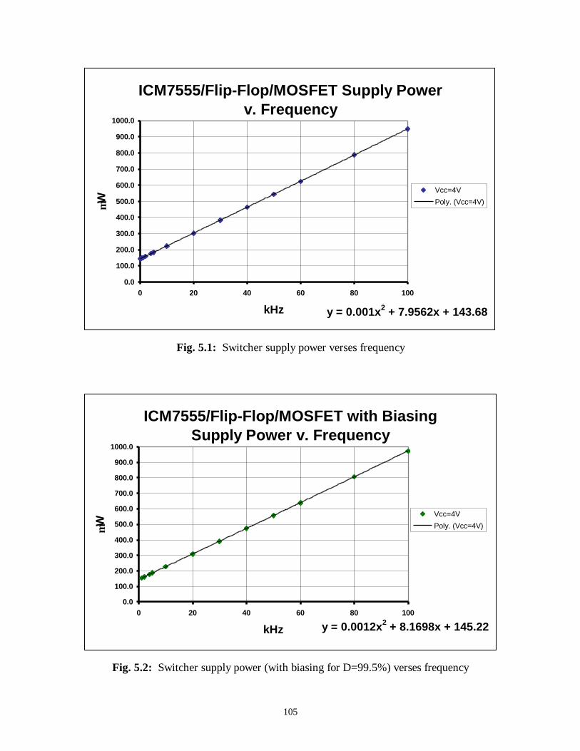
105
ICM7555/Flip-Flop/MOSFET Supply Power v. Frequency
y = 0.001x2 + 7.9562x + 143.68
0.0
100.0
200.0
300.0
400.0
500.0
600.0
700.0
800.0
900.0
1000.0
0 20 40 60 80 100
kHz
µW
Vcc=4VPoly. (Vcc=4V)
Fig. 5.1: Switcher supply power verses frequency
ICM7555/Flip-Flop/MOSFET with Biasing Supply Power v. Frequency
y = 0.0012x2 + 8.1698x + 145.22
0.0
100.0
200.0
300.0
400.0
500.0
600.0
700.0
800.0
900.0
1000.0
0 20 40 60 80 100
kHz
µW
Vcc=4VPoly. (Vcc=4V)
Fig. 5.2: Switcher supply power (with biasing for D=99.5%) verses frequency

106
Now, based upon simplified linear, low-level transformer design equations, a
transformer design spreadsheet has been developed (P. Clower, 1997)[29],[30]. After a few
small modifications to account for square-wave excitation and the addition of the tertiary
winding, this design tool allowed for iterative calculations of transformer efficiency with
varied pot core sizes, ferrite material types, and maximum desired flux density. The pot
core style was selected because of its shielding properties -- important for predictable
converter operation – and ease of winding. Further, ferrite composites are typically
selected for switching power converter applications. Because of their high magnetic
permeability and relatively low loss factors at audio frequencies, ferrite cores are
particularly well-suited for use in square-wave applications where the core is switched
rapidly from full magnetization of opposing polarities[29].
A few assumptions are made which permit the use of the linear transformer design
equations presented above. In linear operation, the maximum induced flux density must
be below the linear cut-off Bo, -- the point at which the permeability slope is no longer
considered linear for the material. This assumption is valid because the maximum induced
flux density is limited here (by design) to well below published Bo. Further, a handful of
reasonable assumptions are made about the approximate equivalent circuit used to derive
these equations:
• Capacitance effects are negligible, or can be accounted as external to thetransformer over the frequency range of interest.
• Leakage reactance effects are negligible – that is, the windings are fully coupled.• Winding resistance is proportional to the turns ratio N.• A lumped loss path (Rcore) accounts for all core losses.• All winding losses are represented as series resistance losses.

107
In most power transformer applications, it is assumed that the excitation is high
enough that self-heating is the limiting factor in core size and a central consideration in its
design; however, that is not the case in this system[31]. As will be shown, the peak primary
power measures about 26 mW and is only transforming energy less than one fifth of the
time (assuming it takes .075 seconds of switching to remove all charge from the bimorph).
Therefore, the criteria normally applied to power transformer design is abandoned here,
and the low-level design equations are used. The important parameters in this case are:
primary RMS voltage, secondary RMS voltage, operating frequency, waveform factor K,
input power, core material and loss factor, core volume and window size, and maximum
flux density[29].
It is assumed that one half of the source energy is successfully switched through the
core, or 4 mW at a .91 Hertz walking pace from the signal plots in Sect. 2.4. The average
output voltage is 4.6 Volts given the voltage window on Cb set in the following section
plus a one volt cushion, and the following calculation for the average equivalent load
resistance is made:
Ω=== k 3.5004.
6.4PC
R2
out
2b
l (5.9)
and
pulse current per mJ 82.191.
004.21
fP
21
Ew
outp =
=
= (5.10)
where

108
frequency Walking
pulse current perEnergy rtransforme through Power
resistance Load
===
=
w
p
out
l
f
EPR
Now, using a bucket capacitance of 300 µF, a 5.35 Volt average peak value on Cb
after each current pulse will decay to 3.80 Volts in .55 seconds (one half of the walking
period), yielding an average voltage on Cb of 4.6 Volts – the target average stated above.
Therefore, the peak secondary-side voltage is set to 5.65 Volts to account for the diode
drop across D5, and the necessary average secondary-side voltage <vs> is found.
( )( ) Volts 62.4de5.555.1
v55.
0
0003.5300Ds =τ= ∫
τ− (5.11)
and, for a 50% duty-cycle square-wave,
Volts 24.9v2vDss == (5.12)
Using the average peak voltage observed in the boot signal, 160 Volts, the average
primary side voltage is calculated in the following way:
Tpeakoff eVV
τ−= (5.13)
and
dteV1
V Tt
0 peakp
−τ
∫τ= (5.14)
where

109
voltageprimary Average
period ON Switcherconstant time Load
voltage off-turn Switcher
voltage signalpeak Average
==τ=
==
p
off
peak
V
TV
V
In this design, where the turn-off voltage is set at 20 Volts by the signal peak detector
circuit, the average primary side voltage is calculated as
Volts 3.67dte160)8ln(T
1V
)8ln(Te16020
Tt
)8ln(T
0p
T
=⋅
=
⋅=τ⇒=
−⋅
τ−
∫
Now, the average secondary current must be determined. Using the output power and
average load resistance, this value is found as follows.
IPR
I lout
ll
2 0045300
87= = ⇒ =.
. mA (5.15)
and
I s ON=
⋅
=
12
112 075
00087 319.
.. . mA (5.16)
where
period ON during current secondaryaverage=ONsI

110
In the previous equation, the average load current is multiplied by the ratio between the
step period and the average ON time for the switcher (with two current pulses per step)
determined by inspection of collected bimorph voltage signals. Further, that value is
divided in half to account for the current gain at 50% switch duty-cycle. Finally, the
average power transferred through the transformer is calculated from the output power
and the transformer ON period in the following manner:
PP
2 .75 t ON
l= ⋅ = ⋅ =..
.0042 75
026 W (5.17)
Because the switching waveforms are square, a waveform factor K of 4.0 is used[31].
Also, from among a stock selection of Ferroxcube cores, the #1408 pot core of “3B7”
ferrite composite was selected because it is the largest practical size for use in an
embedded shoe system. Now, all the information required to develop theoretical loss
calculations at various frequencies has been collected. This information was entered into
the design spreadsheet, and the peak flux density was adjusted for the smallest transformer
loss value at a given frequency. The minimum loss typically occurs at a flux density near
to where the winding losses equal the core losses -- this made a good starting point
around which the flux density was more finely adjusted. By iterating this process over a
range of frequencies, the transformer loss curve is generated. Fig. 5.3 shows this plot
along with the switch system loss plot found in Fig. 5.2; a third plot shows the aggregate
switching losses and reveals the optimal switching frequency.
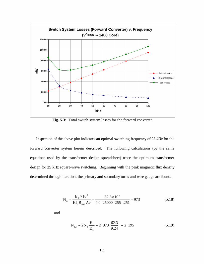
111
Switch System Losses (Forward Converter) v. Frequency (V+=4V -- 1408 Core)
0.0
200.0
400.0
600.0
800.0
1000.0
1200.0
10 20 30 40 50 60 70 80 90 100
kHz
µW Switch losses
X-former losses
Total losses
Fig. 5.3: Total switch system losses for the forward converter
Inspection of the above plot indicates an optimal switching frequency of 25 kHz for the
forward converter system herein described. The following calculations (by the same
equations used by the transformer design spreadsheet) trace the optimum transformer
design for 25 kHz square-wave switching. Beginning with the peak magnetic flux density
determined through iteration, the primary and secondary turns and wire gauge are found.
973251.255250000.4
103.62AeBKf
10EN
8
maxs
8p
p =⋅⋅⋅
×=×
= (5.18)
and
195224.93.629732
EE
N2Np
spt,s ⋅=
⋅== (5.19)

112
with
( ) awg 43110)N2(log10INTG p10p =++= (5.20)
( ) awg 38110)N2(log10INTG t,s10t,s =++= (5.21)
where
gauge wireSecondary
gauge rePrimary wiarea sectional-cross core Effective
density flux Maximumvoltage RMSSecondary
voltage RMSPrimary
count turntertiary andSecondary
count turnPrimary
===
====
=
t,s
p
e
max
s
p
t,s
p
G
GABE
E
N
N
Now, to determine the resistive losses, the length of the windings and their linear
resistivity are found:
feet) in(1.8154.21254.2973
54.212MLTN
L ppp =
⋅⋅=
⋅⋅
= (5.22)
feet) in(5.1554.21226.3145
54.212
MLT2
N
Lt,s
t,s
t,s =⋅⋅=
⋅
⋅= (5.23)
and
Ω=
=
−
4.167967
10L
R
110
G
p
p
p
(5.24)

113
Ω=
=
−
1.20967
10L
R
110
G
t,s
t,s
t,s
(5.25)
resulting in
W µ=⋅
+
= 38RII
NN
P p
2
mag
2
sp
sp (5.26)
W µ=⋅
⋅=+ 175RI
NN
2PP t,s
2
sp
sts (5.27)
where
mA 19.
10
NAf2
10EI
6
2pL
s
6p
mag =
π
×= (5.28)
and
Turns mH/1000 - parameter Material
(mA) current ng Magnetizi
resistance tertiary) (and Secondary
resistancePrimary
windingtertiary) (and secondaryof Length
ndingprimary wi of Length
==
===
=
L
mag
t,s
p
t,s
p
A
I
R
R
L
L
Now, the core losses are found using the core loss parameter Kc and core volume Vc.
W µ=⋅=
⋅=⋅= 5.71495.14.cm
cmmW
VKP 33ccc (5.29)

114
And, the theoretical efficiency of the transformer is calculated.
( )
( )%9.98
26072.175.038.26100
P
PPPPP100
ONt
ctspONt
rtransforme
=++−⋅=
+++−⋅=η
(5.30)
For completeness, the transformer specifications are presented in the following table:
Transformer Specificationsfs 25 kHzNp 973Ns,t 145Gp 43 awgGs,t 38 awgMaterial Ferrite 3B7Core Size #1408 (pot core, d=14mm, h=8mm)Flux Density (max) 255 Gauss
Table 5.3: Transformer specifications
Finally, a similar optimization could be performed for the buck converter topology, but
such a rigorous analysis is not presented here. The natural loss trade-off in the buck
design is between switching and inductor losses; however, inductor losses are so small in
comparison to the transformer losses derived above. As will be discussed in the final
chapter, switching and gate drive losses dominated the buck converter system in practice,
making such a rigorous derivation inconsequential.

115
Chapter 6
Conclusions and Recommendations
This chapter reviews the work presented in this report, discusses complications
encountered in implementing the systems, and compares the results and performance of
each design. It provides conclusions on the efficiency and efficacy of switching converters
in conditioning piezoelectric power, both in general and specifically for the systems
described herein. Finally, it suggests areas for improvement and related future work.
6.1 Results
The work presented here has two parts. The first part was to develop a rugged,
unobtrusive shoe insert for harnessing the compression energy normally dissipated into the
insole of a shoe. A rigid, bimorph PZT transducer was developed consisting of two
THUNDER unimorphs in parallel electrical connection and mounted on opposing sides
of a Beryllium-Copper backplate. The insert was integrated into the heel cup of an off-
the-shelf orthopedic insole. As the insole undergoes heel strikes and subsequent releases,
the bimorph is compressed and relaxed and the PZT material is excited in 31-mode
bending transduction. This excitation produces a train of low-power, high-voltage current
pulses to the load and conditioning electronics.
Once the source was developed and characterized, three power conditioning systems
were compared. The first of these systems was the trivial approach -- to leak the charge

116
through a rectifier circuit and into a capacitive bucket. This direct-discharge method is
simple but inherently inefficient, and an analytical assessment was presented revealing its
poor efficiency/output ripple trade-off. The other approaches applied high-frequency
switching techniques based upon two common, dc-dc direct converter topologies -- the
buck and forward converters. The theory governing switching converters was developed
briefly, and two systems were proposed for implementing hybrids of these topologies.
The system-level concepts were further developed, and rudimentary, self-starting
control electronics were proposed which address the special constraints imposed by the
bimorph source. With the exception of different gate drive circuitry and the presence of a
step-down transformer in the forward converter design, the two conditioning systems are
basically identical. They consist of the following stages: rectification, feed-forward
bootstrap loop, high-frequency switching (and step-down transformation), CMOS ‘555
timing and switch control, load stage ON/OFF control, and output regulation. After these
stages were developed, components were selected and the two switching systems
constructed.
A few of the stages were problematic in practical implementation. The most
troublesome of these was the feed-forward loop and start-up circuitry. In a design where
the source charge is so small and at such a high voltage, the energy loss due to OFF-state
leakage is significant and likely. Therefore, the feed-forward loop must be ensured fully
OFF after the system is bootstrapped. This is accomplished by choosing R2 and R3 so
that they bias the gate of Mf2 fully ON when the start-up latch has been activated. More

117
difficult, however, is ensuring the loop is ON at start-up. The capacitive divider at the
gate of Mf1 (formed by Cff and the channel capacitance of Mf2) must trickle enough
charge into that gate to hold it ON through the threshold Cb voltage of the start-up latch.
If this balance is not correct, the system can take an inordinate amount of time to
bootstrap, or in contrast, be quite lossy when the feed forward loop is OPEN. A second
troublesome design point was the selection of Rc1, Rc2, C1 and C2. Because R1 is 120
MΩ , the leakage current into the comparator inputs and across component capacitances
become significant, making strict mathematical calculations unreliable for design decisions.
Finally, both systems were limited (and their performance degraded) by the scarce
commercially availability of high-voltage, low-power transistor switches. Most BJTs and
MOSFETs intended for high-voltage switching are also designed to support rather high
currents and high-power switch transients. As discussed in the previous chapter, the gate
to channel capacitance and threshold voltage of most high standoff voltage switching
MOSFETs are quite high. They therefore require drive power that is much higher than
acceptable in low-power switching systems. The BS107A was the only commercially-
available, small-signal n-channel FET found suitable for this design, and its 200 Volt
breakdown still limits the input signal range significantly. Moreover, no appropriate p-
channel FETs were found for the buck converter system, and a more lossy, high-voltage
pnp BJT was used instead. Therefore, further work in applying switching converters to
piezoelectric systems should include the design of switching MOSFETs more well suited
to the signal characteristics of the piezoelectric sources.

118
The following figures are representative signals from the forward converter. The
direct converter’s useful power output was negligible -- just enough to operate the control
and switching electronics – and it is therefore not shown here. Fig 6.1 shows the
converter in normal, continuously regulated operation. The three traces are the source
signal (normalized by .02 for easy viewing), the voltage across the bucket capacitor, and
the regulated 3 Volt output providing 1.3 mW continuously into a resistive load. Fig. 6.2
shows the same system in discontinuous regulation. It highlights the load-switching
function of the conversion electronics that prevent an over-current into the load from
completely draining the bucket capacitor and initiating the bootstrap process from scratch.
Finally, Fig. 6.3 shows the charging voltage across a 300 µF bucket capacitor through
thirty-six steps on the bimorph transducer. This plot allows for appropriate comparison
between the forward converter efficiency and the efficiency of direct-discharge using the
same source and load capacitor.
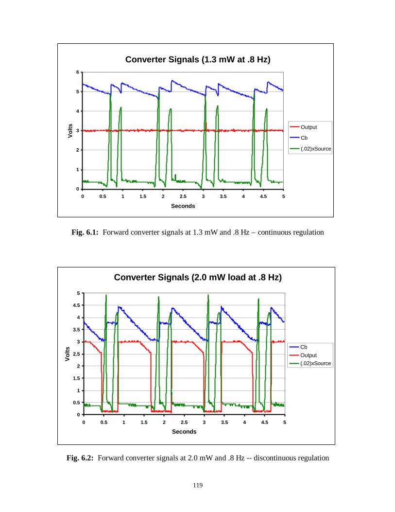
119
Converter Signals (1.3 mW at .8 Hz)
0
1
2
3
4
5
6
0 0.5 1 1.5 2 2.5 3 3.5 4 4.5 5
Seconds
Vol
ts Output
Cb
(.02)xSource
Fig. 6.1: Forward converter signals at 1.3 mW and .8 Hz – continuous regulation
Converter Signals (2.0 mW load at .8 Hz)
0
0.5
1
1.5
2
2.5
3
3.5
4
4.5
5
0 0.5 1 1.5 2 2.5 3 3.5 4 4.5 5
Seconds
Vol
ts CbOutput(.02)xSource
Fig. 6.2: Forward converter signals at 2.0 mW and .8 Hz -- discontinuous regulation

120
Bucket Voltage With 36 Steps using Bimorph
0
2
4
6
8
10
12
14
0 2 4 6 8 10 12 14 16 18 20
Seconds
Vol
tage
Fig. 6.3: Bucket voltage with 36 steps using the bimorph insert
To calculate the efficiency of the forward converter electronics, the power output
must be normalized to the walking frequency used throughout this report, .91 Hz.
mW 48.13.18.91.
Pf
fP data
data
walkingout =⋅
=⋅
= (6.1)
and
% 6.174.8
48.1PP
source
oute ===η (6.2)
Now, for completeness, the original Media Laboratory results are provided (See
Appendix A).

121
mW 356.P ML_out =
and
% 8.19ML_e =η
Finally, for a better comparison between conditioning systems, Fig. 6.3 is provided. With
36 steps taken over 18 seconds, the graph excitation frequency is
Hz 21836f graph == (6.3)
Assuming the same boundary voltages on the bucket capacitor as set in the Media
Laboratory design and the same average power consumed by the RFID device during the
ON period
( ) ( ) mJ 4.1866.121030021VVCb
21E 2262
min2
maxt =−⋅×⋅=−⋅= − (6.4)
and
secmW 53.3T21.5T
4.018.TE
P ONONON
tON =⇒=== (6.5)
From the graph, the time required to charge the bucket cap from 6 to 12.6 Volts is
approximately 10 seconds. Using this information, the average power supplied to the

122
RFID system were it powered by the bimorph source through the Media Laboratory
conditioning electronics is
mW 618.53.310
53.3291.
00521.T
Tf
fPP ON
graph
walkingONbucket =
+
⋅=
= (6.6)
This translated into an efficiency of
% 4.70084.Pbucket
e ==η (6.7)
The above efficiency is a better value by which to judge the performance of the switching
converter developed in this report. By comparison to the original Media Laboratory
design using the same bucket capacitor and source, the forward converter hybrid
demonstrated greater than twice the conversion efficiency of the direct-discharge method.
Therefore, it has been shown that high-frequency switching converter hybrids can be
used to condition power from a piezoelectric shoe insert. In theory, they are the most
appropriate means to match a high-impedance, capacitive source to a large bucket
capacitor. The switching function and energy storage devices form an active impedance
match and provide current gain to an otherwise limited charge source. It is these high-
frequency switches and magnetics, however, which are most likely responsible for the
power loss associated with converting the source energy via switching techniques into a

123
useful form. The system losses are high in comparison with the energy available from the
bimorph source, resulting in a lower efficiency than anticipated. But, the buck and
forward converter system presented here functions with a higher efficiency than previous
systems under similar constraints. Moreover, it have the potential to yield much higher
power outputs with further investigation.
In summary, while the raw electrical efficiency is slightly lower than that obtained in
the original Media Laboratory design, the energy harnessing system developed herein
yields more than four times as much power and has a normalized efficiency two times as
high as that design. Equally important is that this system provides that power
continuously. The hybrid forward converter system presented in this report is therefore a
notable advance in piezoelectric energy harvesting in shoes.
6.2 Conclusions
Although the theory developed in this report justifies the use of switching techniques
in efficiently converting that energy to a usable form, there are obviously some practical
limitations to the systems presented. Measurements of source current into the primary and
load current transferred from the secondary reveal that very little current gain truly occurs
between the input and output ports of the switch/transformer combination in the forward
converter hybrid. Further, similar results were encountered when one examines the energy
transferred through the series switch and inductor in the buck converter. It is likely that
much of that loss is due to switching dissipation, unanticipated losses in the transformer,

124
and directly loading of source current with the series switch and gate drive used in the
buck system.
Switching dissipation is a function of the momentary overlap of voltage and current
waveforms across a transistor during switch transitions. When a power semiconductor is
either ON or OFF, its power dissipation is relatively small and predictable. However,
during transitions from either state to the other, high voltage and high current waveforms
can occur simultaneously. The losses associated with this overlap are usually
inconsequential, but in low power systems like the ones presented here, they can be quite
significant[20]. It is often assumed that the transition waveforms are linear with a known
average overlap period tf. Where tf is.01 µs for the BS107A power transistor used in these
systems, the energy lost per transition in the forward converter switch is
nJ 15.2
1001.7.6
00319.3.62
2tIV
dtivW
6
fdcdcQ
t
0 Qdissf =
×⋅⋅===
−
∫ (6.8)
or, for the energy per switcher ON period,
J µ=⋅⋅×=⋅⋅= − 56.075.500001015.Tf2WW 9onsdissON_diss (6.9)

125
The switching loss in the forward converter is therefore probably inconsequential. For the
buck converter in which a series pnp transistor was acutally used, however, the tf is
typically .5 µs, and the energy loss per switcher ON period is
J µ=
⋅×= − 28
01.5.
1056.W 6ON_diss (6.10)
Though both systems experience some switching loss, neither of the previous
calculations account for all of the energy lost through the switch and filter systems. It is
therefore likely in the forward converter that much of the conversion loss is associated
with unanticipated energy dissipation in the transformer. A variety of mechanisms will
introduce loss in the transformer. In addition to winding resistance and core loss, the two
discussed in Chapter 5, hysteresis, eddy currents and leakage flux will also contribute.
Further, although the assumptions and first-order approximations used to characterize the
transformer designed herein work well for medium- and high-power applications, they
may break down for low-power designs.
Finally, the gate drive circuitry for the buck converter hybrid is inherently lossy. The
series pnp switching transistor must be referenced to the high-voltage signal, and charge is
taken directly from the bimorph source to supply the base with excess charge
concentration for the turn-on transition. This charge is lost during the subsequent turn-
off. Further, unlike the single n-channel MOSFET switch required in the forward
converter, the pnp transistor will dissipate current through the base drive circuit during the

126
entire ON period. In a design in which each current pulse provides only 44 µC of charge
on average, these losses can be significant.
In summary, there are variety of loss mechanisms which could contribute to the low
system efficiencies observed in both the buck and the forward converter systems.
Although it is difficult to characterize them completely or discern which mechanism is
primarily responsible, it is likely that the transformer in the forward converter and the base
drive circuit in the buck converter are the most significant contributors. Work continues
therefore to better characterize and address these loss mechanisms.
6.3 Recommendations
There remain a few areas which should be addressed in future work. As discussed at
the conclusion of Chapter 2, a better physical impedance match between the insole
material and bimorph could be developed to improve the transducer efficiency by up to
40%. This modification could be as simple as placing a rigid plastic heel cup in between
the insole fabric and the bimorph insert to focus the dispersed heel strike force onto the
center of transducer. Further, switching transistors more well-suited to piezoelectric
source signals should be designed, and loss mechanisms in the switch drive and
transformer more rigorously confronted. Specifically, exploration of low power gate drive
circuits, soft switching techniques, and optimized transistor geometries are pertinent to
reducing switching losses, and ways to further reduce losses in the step-down transformer
should be investigated. Finally, as layout is often just as important to the performance of a
switching converter as component selections, a printed circuit board with a more optimal

127
layout could be designed. A better component layout could reduce switching noise and
eliminate stray resonances which may be the underlying reasons behind degraded
performance.
Beyond improvements to these designs, the most appropriate next step is to integrate
the systems with some low-power, body-worn electronics. The MIT Media Laboratory
has previously demonstrated an RFID transmitter using the direct discharge circuit
discussed in Chapter 1; however, a variety of other applications could be explored. One
example is to embed the conditioning system into the heel of a military boot and use the
scavenged energy to operate a “quick look” GPS system for troop positioning, navigation
or emergency recovery. In such an application, the piezoelectric insole and conditioning
electronics could be separate components within the boot. As the insoles wear out, they
could be replaced or upgraded, modularly linked to the electronics embedded in the heel
via a weatherproof connector inside the boot. This is just one example of a useful and
feasible application of piezoelectrically-scavenged shoe power. There are myriad others,
and, with a few minor improvements and minimal adaptation to the systems presented in
this report, switching converters could be used to condition the power for many future
body-worn, shoe-powered devices.

128
Appendix A
Functional Description and Efficiency of MediaLaboratory Conditioning Electronics
The principle objective of this project was to design an integrated, rugged piezoelectric
shoe insert and efficient power conditioning electronics, improving upon earlier work in
this area. For comparison, the previous benchmark must be established. This appendix
provides functional description of the Media Laboratory design followed by an analysis of
its efficiency.
A.1 The Media Laboratory Design
For ease of reference, the schematic is included in the following figure.
Fig. A.1: Schematic of power conditioning electronics and encoder circuitry for the shoe-powered RFID tag[5]
This novel design utilizes the energy scavenged from either the THUNDER™ or the
PVDF stave to encode and transmit a periodic, ASK-modulated, RFID signal. The
transmission is received by a local base station that emits an audible chirp upon identifying

129
the transmitter. This type of system has immediate application in an active environment
where multiple users periodically transmit their identity to the local surroundings, enabling
dynamic, centralized decisions to be made affecting the environment or updating state
information about the work-place.
The signal from the piezoelectric source is full-wave rectified through the 500mA
diode bridge D1. As the source signal ramps up, charge is transferred to an electrolytic
“bucket capacitor” C1 whenever the source voltage overcomes the voltage already
supported by this capacitor plus two diode drops. As C1 charges beyond 12.6 Volts (or
the Z1 zener breakdown voltage plus the diode drop across the base-emitter junction of
Q1), Q1 is forced into conduction, in-turn activating Q2 (and latching Q1). With Q1 on,
the high-side of C1 now has a current return path to ground and discharges through the
Maxim MAX666 LDO linear regulator U1. The phrase “load-switching” was used
throughout this report to describe that latching action.
The regulator is biased to provide a stable +5 Volts to the serial ID encoder (U2)
and RF transmitter (U3), as long as C1 remains above +5 Volts (plus the regulator drop
out voltage). When the voltage across C1 reaches approximately 4.5 Volts, the low-
battery in pin (LBin on U1) is pulled below its threshold, driving the low-battery out pin
(LBout) to ground momentarily. This negative pulse though C3 turns Q1 off, thus
deactivating Q2 and renewing the C1 charging cycle. Note that R1, R2 and R3 serve to
bias Q1 and Q2 and to show C1 a very high load impedance when the Q1-Q2 latch is
deactivated. Further, R4 and C2 were included to better match the source impedance to
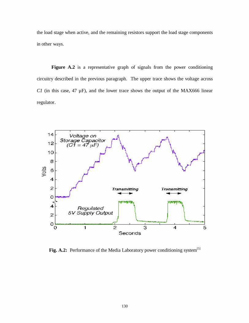
130
the load stage when active, and the remaining resistors support the load stage components
in other ways.
Figure A.2 is a representative graph of signals from the power conditioning
circuitry described in the previous paragraph. The upper trace shows the voltage across
C1 (in this case, 47 µF), and the lower trace shows the output of the MAX666 linear
regulator.
Fig. A.2: Performance of the Media Laboratory power conditioning system[5]

131
A.2 Efficiency Analysis
The power output and system efficiency are determined from the previous graph.
Through examination of the first full transmission and charging cycle ( ~ 2.1 to 3.7
seconds), the following information is collected:
Volts 5 voltage Source seconds.6 )(T period ON
Volts 6 VVolts 12.6 V
8 count Step seconds1.6 (T) period Cycle
ON
min
max
==
==
==
Now, determining the average power delivered to the regulator and RFID electronics by
C1 and normalizing the power to the average walking frequency used in this report,
( ) ( ) mJ 12.366.12104721VVCb
21E 2262
min2
maxt =−⋅×⋅=−⋅= − (A.1)
mW 21.56.
00312.TE
PON
tON === (A.2)
and
mW 356.6.16.
6.1891.
00521.T
Tf
fPP ON
graph
walkingONbucket =
⋅=
= (A.3)
where
capacitor bucketby suppliedpower average ,Normalized
period ON during Cby suppliedPowerperiod ON during pliedEnergy sup
b
==
=
bucket
ON
t
P
PE

132
The average raw power published in the Media Laboratory report was 1.8mW at
approximately .91 Hertz. Assuming that value is representative for the method used to
excite the transducer in Fig. A.2, the electrical efficiency of that system is
% 8.190018.Pbucket
e ==η (A.4)

133
Appendix B
Matlab™ Script for Direct-Discharge Model
% Nathan Shenck% A Demonstration of Useful Electric Energy from Piezoceramics in aShoe
clear all;close all;
% a = time required to fully depress transducer% Qt = total charge accumulated on transducer% T = average period between current pulses% vl = average load voltage% Rd = dielectric leakage equivalent resistance% Rl = load resistance% Re = Rd//Rl% Cb = bucket capacitance% Cp = total capacitance of transducer% Ce = Cb + Cp
% define system parametersT=.55;Rd=10^7;Cp=143*10^(-9);Vdd=.60;Vl=0;
% define equivalent current bursta=.1;Qt=5.9*10^(-5);Iq=Qt/a;
% find/define "way point" times td, b and ctd=-(Rd*Cp)*log(1-2*Vdd/Iq/Rd-Vl/Iq/Rd);b=a-td;c=T-a;
% determine Re with changing Rl'si=1:32;Rl=10.^((i+32)/8);Cl=10.^((i-48)/4);Re=((1/Rd)+1./Rl).^(-1);Ce=Cp+Cl;
% determine Ce with changing Cl'sTe=(Re'*Ce);Tl=(Rl'*Cl);
for i=1:32 for j=1:32
Va(i,j)=(Iq*Re(i)-2*Vdd*(Re(i)/Rd))*(1-exp(-b/Re(i)/Ce(j)))+Vl*exp(- b/Re(i)/Ce(j));
% determine total energy transfer to load after one step cycle (inparts)

134
E_total11(i,j)=((Iq*Re(i)-2*Vdd*Re(i)/Rd)^2)*(b-2*Te(i,j)*(1-exp(-b/Te(i,j)))+(.5)*Te(i,j)*(1-exp(-2*b/Te(i,j))))/Rl(i);
E_total12(i,j)=(2*Vl/Rl(i))*(Iq*Re(i)-2*Vdd*Re(i)/Rd)*(Te(i,j)*(1-exp(- b/Te(i,j)))-(.5)*Te(i,j)*(1-exp(-2*b/Te(i,j))));
E_total13(i,j)=(Vl^2/Rl(i))*(.5)*Te(i,j)*(1-exp(-2*b/Te(i,j)));
E_total2(i,j)=((Va(i,j)^2)/Rl(i))*Tl(i,j)/2*(1-exp(-2*c/Tl(i,j))); endend
E_total=E_total11+E_total12+E_total13+E_total2;
% maximum E through direct-dischargeMax_E=max(max(E_total)')
% possible E from CpE_poss=.5*Qt^2/Cp
% plotsfigure(1);mesh(log10(Cl),log10(Rl),E_total*1000)ylabel('Resistance - Log(Ohms)');xlabel('Capacitance - Log(F)')title('Total Energy into Various Loads ( mJ)')figure(2);mesh(log10(Cl),log10(Rl),E_total*1000)ylabel('Resistance - Log(Ohms)');xlabel('Capacitance - Log(F)')title('Total Energy into Load (mJ) -- <Vl>=0 Volts')view(130,30);figure(3);mesh(log10(Cl),log10(Rl),E_total*1000)ylabel('Resistance - Log(Ohms)');xlabel('Capacitance - Log(F)')title('Total Energy into Various Loads ( mJ)')view(-120,30);figure(4);mesh(log10(Cl),log10(Rl),E_total*1000)ylabel('Resistance - Log(Ohms)');xlabel('Capacitance - Log(F)')title('Total Energy into Various Loads ( mJ)')view(0,90);

135
References
[1] Pentland, A. S., “Wearable Intelligence,” Scientific American, Vol. 276, Nov. 1998. [2] “Land Warrior Program,” URL: http://www-sscom.army.mil/ prodprog/lw/index.htm,
U. S. Army Soldier Systems Center [Natick], Natick, MA, 1999. [3] Starner, T., “Human Powered Wearable Computing,” IBM Systems Journal, Vol. 35,
No. 3&4, 1996, pp. 618-629. [4] Fletcher, R., “Force Transduction Materials for Human-Technology Interfaces” IBM
Systems Journal, Vol. 35, No. 3&4, 1996, pp. 630-638. [5] Kymissis, J., Kendall, J., Paradiso, J. and Gershenfeld, N., “Parasitic Power Harvesting
in Shoes,” Second IEEE International Conference on Wearable Computing (ISWC),October 1998.
[6] “Walking Power Electronics,” Popular Mechanics, March 1999, pg 16. [7] Crawley, E., de Luis, J., “Use of Piezoelectric Actuators as Elements of Intelligent
Structures,” Department of Aeronautics and Astronautics, Massachusetts Institute ofTechnology, June 1987.
[8] Miller, S., Hubbard, J., “Theoretical and Experimental Analysis of Spatially Distributed
Sensors on a Bernoulli-Euler Beam,” C. S. Draper Laboratory C-5953, July 1987, pp.1-22.
[9] “Piezoceramic Tutorial,” URL: http://www.piezo.com/appdata.html, Piezo Systems,
Inc., Cambridge, Massachusetts, 1999. [10] Berlincourt, D., “Piezoelectric Crystals and Ceramics,” Ultrasonic Transducer
Materials, ed. O.E. Mattiat, Plenum Press, New York, New York, 1971. [11] Dausch, D. and Wise, S., “Compositional Effects on Electromechanical Degradation of
RAINBOW Actuators,” NASA, Hampton, Virginia, 1998.
[12] Mossi, K., “Thin Layer Composite Ferroelectric Driver and Sensor Characterizationwith Application to Separation Flow Control,” Old Dominion University, 1998.
[13] “THUNDER™ Product Data,” Face International Corporation, 1997.
[14] Chandrakasan, A. and Shenck, N. S., “Piezoelectric Energy Conversion in Walking”
Independent 6.961 report to the Department of Electrical Engineering and ComputerScience, Massachusetts Institute of Technology, 1997, pp 2-3.

136
[15] Gray, Dwight E., ed., et al., American Institute of Physics Handbook, 3rd Edition,McGraw Hill, 1972, pp 2.68-69.
[16] Feynman, R. P., Leighton, R. B. and Sands, M., “Elasticity,” The Feynman Lectures on
Physics, vol. II, Addison-Wesley Publishing Company, Reading, Massachusetts, 1965,pp. 38- 8-11.
[17] Cottrell, A. H., The Mechanical Properties of Matter, John Wiley & Sons, Inc., New
York, et. al., 1964, pp. 124-8.
[18] Piezo Film Sensors Technical Manual, Amp, Incorporated, 1993.
[19] Toda, M., “Theory of OPT Rotary Generator,” AMP Sensors, Inc., 1997, p. 1.
[20] Edgerton, H., Electronic Flash, Strobe, New York, New York, McGraw Hill, 1970.
[21] Kassakian, J., Schlecht, M. and Verghese, G., Principles of Power Electronics,Addison-Wesley Publishing Company, Inc., Reading, Massachusetts, 1991, p 103.
[22] Horowitz, P. and Hill, W., The Art of Electronics, Cambridge University Press,
Cambridge, England, 1980, p 360.
[23] Landesman, E., “A Unifying Derivation of Switching dc-dc Converter Toplogies,”PESC Record, Institute of Electrical and Electronic Engineers, 1979, pp 239-243.
[24] Carleson, A. B. and Gisser, D. G., Electrical Engineering Concepts and Applications,Addison-Wesley Publishing Company, Reading, Massachusetts, 1990, pp. 677-89.
[25] “Ultra Low-Power, Low-Cost Comparators with 2% Reference – MAX931-934 (Rev.
1)” [Product Data Sheet], URL: http://209.1.238.250/arpdf/1219.pdf, MaximIntegrated Products, Sunnyvale, California, February 1997, pp. 11-3.
[26] Turko, B. T., Smith, R. C., “A Precision Timing Discriminator for High DensityDetector Systems,” IEEE Transactions on Nuclear Science, vol. 39, no. 5, pt. 1, Oct.1992, pp. 1311-15.
[27] “General Purpose Timers – ICM7555/7556 (Rev. 2)” [Product Data Sheet], URL:http://209.1.238.250/arpdf/1503.pdf, Maxim Integrated Products, Sunnyvale,California, November 1992, pp. 6-7.
[28] “Dual Mode 5V/Programmable Micropower Voltage Regulators – MAX663/MAX664/MAX666 (Rev. 1)” [Product Data Sheet], URL:http://209.1.238.250/arpdf/1330.pdf, Maxim Integrated Products, Sunnyvale,California, July 1996, p. 5.

137
[29] “Linear Ferrite Magnetic Design Manual,” Ferroxcube, Division of Amperex ElectronicCorp., 1971, pp. 1-12.
[30] Conversation with Clower, P., C. S. Draper Laboratory, May 1st, 1999.
[31] Hurley, W. G., Wölfle, W. and Breslin, J. G., “Optimized Transformer Design:Inclusive of Frequency Effects,” paper presented to the V IEEE International PowerElectronics Congress, Cuernavaca, Mexico, October 1996.