Embed Size (px)
Citation preview

Jurnal Kejuruteraan 13 (2001) 99-114
A Comprehensive Computational Design for Microstrip Passive and Active Linear Circuits
EI-Sayed A. EI-Badawy Said H. Ibrahim
ABSTRACT
This paper presents a user-oriented comprehensive computational program for designing linearactive and passive micro'S/rip circuits such as amplifiers, oscillators, mixers. lowpass jilters, and cuoplers. The substrate parameters and the characteristic impedance of the microslrip lines are given /0 the program as a common statement. Examples for the design of a 3 GHz high gain amplifier, 2.6-GHz oscillators. ring coupler operated at 3 GHz. and maximally-JIat lowpass filter operated at 2 GHz with 0.75 GHz cwofi frequency are conducted. The introduced program ;s compared to other available ones.
Keywords: Computational Micros/rip Design. Microwave Circuits, Computer Aided Design for Microwave Circuit.
INTRODUCTION
Since the mid-1917s, a number of computer programs for microwave circuit design had become commercially available. Some well-known microwave computer-aided engineering software package are SUPER COMPACT (from Compact Software, Inc, 2000), TOUCHSTONE (from EEsof, Inc. 1997), and others. All of these programs have certain advantages and some disadvantages.
In this paper we introduce a new version, HHSS2, of our previous computational program, EI-Motaafy et al. (\995). In the comparison with the previous version HHSS2 has the following additional features:
I. It performs two-section branch line couplers. 2. It takes into consideration full discontinuities of microstrip lines. 3. It performs complete design of integrated circuits such as mocrostrip
receiver with amplifiers, oscillator, mixer, and lowpass filter. 4. It modofies the format of the output files to suit the particular application. 5. It cover with application. 6. It can be used in case of changing the transistor unconditional stability
to potensial unstability and vice versa, either by connecting a cascaded resistor to the transistor terminals.
GENERAL DESIGN METHODOLOGY OF THE SOFTWARE
I. Depending on the type of the circuit (active or passive) and the internal parameters of the speCified circuit, the software displays all the required parameters that can be specified by the user.

100
2. The substrate parameters of the microstrip H, r, and T are given as common parameters. If the user needs to change these parameters, the software can interact with himlher to enter the new substrate parameters.
3. The software can interact with the user for some selection and assumptions inside the specified circuit such as the number of sections in lowpass filter, or branch coupler, and the bandwidth of the Wilkinson hybrid.
4. After the entry of all parameters required by the user for the specified circuit design, the software performs a complete analytical design with appropriate lengths and width of the micros trip lines of the designed circuit.
S. The software introduced an optimum selestion of circuit elements to fulfill some requirements. These requirements include: a) unconditional stability, b) pOlential unstability, c) simultaneous conjugate match, d) changing the transistor stability, e) feedback circuit parameters tomaximize SII' 0 optimum termination for the output circuit to get the maximum output power, and g) optimum selection of [s] parameters (with the optimum feedback stubs at different frequencies or cascaded resistors) to achieve the transistor changes from unconditional stability to potential unstability and vise versa.
PROGRAM DESCRIPTION
The current developed program, HHSS2, is used for the design of linear active and passive circuits using microstrips techniques. Appendix I illustrates the main architecture of the software.
DESIGN OF MICROWAVE AMPLIFIERS
The program performs a complete analy tical design of microstrip amplifiers, (Ibrahim 2000; Gonzalez 1997). The [S] parameters of the used transistor and the operating frequency are given to the program while the substrate parameters (relative permittivity E" dielectric thickness (H), conductor thickness (T), and Zo are considered as a common statement. The program performs the stability of the used transistor (Bodaway 1967). For potential unstable transist<;lf, the user can call a subroutine, called RCAS, to cascade a resistor at the output of the transistor. According to the optimum selection of the value of the cascaded resistor, the transistor will be unconditional stable and the simultaneous conjugate match can be achieved (EI-Motaafy et al. 1995, 1990). The program can perform a complete analytical design of input and output matching circuits without using the Smith chart. Using the subroutines MATCHt and MATCH2, the matching circuits can be performed using stub line of given Zo with different lengths or Ag/8 (3Ag/8) stub lines with different values of Zo(Encelbrecht 1965; Ha 1981). The user can select the type of stub (open/short, single/balanced) used for the design of the matching circuits. The final lengths of the matching circuits are given in mm, radians, or as normalized lengths using the subroutine FLEN.
J

101
DESIGN OF MICROWAVE OSCILLATORS.
Transistor oscillators can be designed using either bipolar or GaAs FET devices (Stassiades et al. 1992; Holdzman & Roberston 1992). Using the [S1 parameters of the active element, the design of the microwavw oscillator is a follows; I) Check of the transistor stability. For unconditional stable transistor, the feedback circuit (open/shon-singlelbalanced stub at the emitter/ source terminal) is designed to get the potential unstability (Gentitle 1987). In addition, the feedback circuit can be used to maximize the value of SII at the given f o. Subroutines STABLE and FB are used for stability considerations and feedback circuit design, respectively 2) Analytical design of the input termination circuit (open/short stub at the base/gate) . to get maximum reflection coefficient at the transistor output; 3) Calculation of the transistor small-signal output impedance; 4) Analytical design of the output marching circuit so that the load impedance is related to the transistor small-signal output impedance. 4) Analytical design of the output matching circuit so that the load impedance is related to the transistor small-signal output impedance by the relations RI = Rw/3, and XI = - Xw, (Dobrowolski 1991). Subroutines xx and XXI are used for the design of the output matChing circuit.
DESIGN OF MICROWAVE MtXERS
The program is suitable for diode and FET mixers (Maas 1986). Subroutine SELM is used to select a diode mixer (Hewlett Packard Appl. Notes 995 and 963) or a FET mixer. For a diode mixer, subroutine MIXER I is used for diode mixer circuit design by calculating the forward and backward impedance and then the hyperbolic mean impedance, while subroutine MIXER2 is used for diode mixer circuit design by calcuting the input impedance of the diode for the given equivalent circuit. For Fet mixer citcuit design, subroutine SGM is used for single-gate FET mixer circuit design. The design of a FET mixer is performed either by the lumped FET model or by the [S1 parameters of the FET. Subroutine FETME is used for input impedance calculation from the FET lumped model, while subroutine FETMS is used for input impedance calculation from the given [S1 parameters. Subroutine xx is used for matching circuit design for both diode and FET mixers.
DESIGN OF MICROWAVE COUPLERS
The program is used for the design of several types of microwave hybrid couplers (Hewlett Packard Appl. Note 963) such as branch-line couplers with different number of sections (N), ring couplers, Wilkinson couplers, Lange couplers, and coupled line-couplers.
Design of coupled-lille couplers A subroutine CLINE is used for the design of the structure of coupled-line couplers for different values of the coupling factors C ~ 3 (Garg & Bahl 1979). The calculation of the optimum values of strip width (W), strip separation (S), and coupler length (L) is staned by initializing the program by the initial values of Wand S, then calculating the corresponding values of even and odd mode impedances (Z~, Zoo) from the capacitive mode equivalent circuit. E,. and the electrical length of even and odd modes

102
(8 ,8 )are calculated for a given value L. The average value of the electrical len'gth is checked to equal 90' with a specified tolerace. Getting the optimum value of the coupler electrical length, the value of Z, is compared with Zo with a specified tolerance by changing the values Wand S.
Design oj branch·line couplers A subroutine BRANCH is used for the design of one-section rectangularl circular branch-line cuoplers with C <: 3 dB and also for the design of twosection rectangular branch-line cuoplers (Fusco 1987; Collin 1992). The program calcuted the impedances of shunt and series arms and the corresponding E,,,, A" widths, and lengths for given fo and C.
Design oj ring cuoplers A subroutine RING is used for the design of the structure of the rate-race (ring) coupler. The program calculates the impedances of the lines forming the coupler and the corresponding widths, E,,,, A" and lengths for given fo and C (Fusco 1987; Collin 1992).
Design oj Wilkinson couplers A subroutine WtLK is used for the design of differrent structures of Wilkinson couplers. The program calculates the values if resistor and Zo of Ihe lines forming the structure with the corresponding E,IT' A" and lengths (Fusco 1987; Collin 1992).
Design oj Lange couplers The basic equation for the Lange coupler circuit design is (AI.Anwar 1999; Osmani 1981):
c= (N -I)(l-(Z~ /Z~)2 ) (N -1)(1 + (Z~ / ZM)')+ 2(Z~ /Z~)
where: C ; the coupling coefficient N ; even number (usually equal 2 or 4) Z~ : odd mode impedance of the coupler line Z : odd mode impedance of the coupler line ~ .
A subroutine LANGE is used for the design of the Lange couplers (Lange 1969) for diffferent values of the number of the strips M and C. The program calculates the even and odd mode W IH ratios, S, W, E,,,, Zoo' Z~, and L. The program uses the equations outlined in (Ou 1975).
DESIGN Of LOWPASS FILTERS
The program uses the lowpass prototype filter C (Fusco 1987; Collin 1992) for the design of a low pass filter. A subroutine LPF is used for the design of this lowpass filter. The program takes into considerations of the effect of the step discontinuities and the equivalent end·effect length. Either maximally flat or Chebyshev lowpass prototype filters are used in the design of the lowpass filter. The program calculates both lumped and distributed structures

103
of the lowpass filter for given N. cutoff frequency (f). f. and Z. of shunt capacitances and series inductances. The program calculates the attenuation at f,.
EQUIVALENT [SI PARAMETERS FOR A TRANSISTOR CONNECTED WITH A SERIES FEEDBACK STUB
A subroutine TRFB is used for the calculation of the equivalent [S) parameters of a transistor connected with a selected feedback stub at different frequincies. The proram deals with single or balanced open/short stubs. This subroutine is used for transistor stability change from unconditional stability to potential unstability.
EQUIVALENT [SI PARAMETERS FOR A TRANSISTOR CONNECTED WITH A CASCADED REStSTOR
A subroutine TRRCA is used for the calculation of the equivalent [S) parameters of a transistor connected with a selected cascaded resistor at different frequencies . This subroutine is used for the transistor stability change from potential unstability to unconditional stability.
DESIGN OF A HIGH GAIN 3-GHZ AMPLIFIER
Table I shows the input parameters and the output parameters (results) of the 3-0Hz amplifier circuit design .
TABLE 1. Input and Output parameters of a 3-GHz microstrip amplifier circuit design
Input Parameters
The substrate/e parameters with 50-.0 normalized impedance are: £,=2.33, H=0.7874 mm, T=0.OO5 mm HXTR 6101 bipolar transistor wilh [S] parameters al 3 GHz are S, = 0.57 L 173' S21 = 2.2 L 48° SOl = 0.043 L 25' S" = 0.77 L 58°
Output Parameters
Transistor stability considerations: 1l=0.393 L 140.50, K=1.25 (the transistor is unconditional stable) Input stability circle: R, (radius of input stability circle) = 0.5573. and Cs (center of input stability circle) = 1.65 L 173.52° (outside is stable) Output stability circle: RL (radius of output stability circle)= 0.21, and C
L (center of output stability
circle) = 1.26 L 62.64° (outside is stable). Complex. conjugate match at the input port: r
l (source reflection
coefficient) = 0.776 L 174.5°. and Z, = 0.126-jO.04712Q. Complex conjugate match at the output port: r
L (load reflection coefficient) =
0.878 L 62.64°, and Z, = 0.236-j 1.26 Q.

104
Table 2 shows the length and widths of the input and output matching circuits of the designed amplifier.
TABLE 2. Lengths and widths of input and output matching circuits of the 3~GHz microstrip amplifier
Length and widths of microstrip lines
Width of microstrip lines Length of series lines Length of open circuit ba1anced stub. or Length of short circuit single stub
Input matching Output matching circuit
2.408 mm 3.145 mm 10.337 mm
13.1883 mm
circuit
2.408mm 14.82 mm
12.486 mm 15.193 mm
Figure I gives the S" (dB). and S" (dB) versus frequency in GHz. Figure 2 shows the schematic diagram of the disigned 3-GHz high gain amplifier.
13 10
N 7 N 4 '" <id I
-2 N -5 '" -8 -
-II
'" -1 4 -17 -20
Frequency (GHz)
FIGURE I. IS"I. IS "I and IS"I in (dB) versus frequency for the 3-GHz amplifier.
B
Ope1\
FIGURE 2. Schematic diagram of 3-GHz high gain amplifier. (A) Input matching circuit using openlbalanced stub. (B) Output-matching circuit using openlbalanced stub.

105
DESIGN OF 2.6·GHZ OSCILLATOR
Table 3 shows the input parameters and output parameters (results) of the 2.6·0Hz oscillator circuit design.
TABLE 3. Input and Output parameters of the 2.6-GHz microstrip oscillator circuit design
Input parameters
The subtrate parameters with 50 Q normalized impedance are: Er = 2.33, H ~ 0.7874 mm, and T ~ 0.005 mm. HXTR 410 I bipolar transistor with [S] parameters at 2.6 GHz are:
S" ~ 00.9817 L 132.106° S" ~ 1.96511 L ·9.43° S" ~ 0.065 L 11.599°, and 5" ~ 1.10323 L ·62.131°.
Output parameters
Transistor stability considerations: /!. ~ 0.98 L 74.64°, and K ~ 0.82 (the transistor is potential uns~able) The terminating circuit designed: the terminating circuit is designed to get max.imum reflection coefficient at the transistor output. The selected elements of the terminating circuit are an open circuit stub at the emitter terminal and a short circuit shunt stun at the base terminal. Design of output matching circuit: The impedance and the corresponding reflection coefficient at the output of the terminating circuit are ZL = 1O.23 M lS.8 Q and r
L ~ 0.68725 L 143.63°.
Table 4 shows the length and width of the terminating and the matching circuits of a 2.6 OHz microstrip oscillator. Figure 3 shows the final schematic of the designed oscillator.
TABLE 4. Length and width of the terminating circuit and the matching circuit of a 2.6-GHz microstrip oscillator
Terminating circuit
Length of emitter open circuit shunt stub ~ 11.94 mm Length of base short circuit shunt stub ~ 3.645 mm
Matching circuit
Width of microstrip lines = 2.23 mm Length of series line = 9.496 mm Length of open circuit single (balanced) shunt stub ~ 14.2285 (9.94) mm
DESIGN OF A RING COUPLER
Table 5 shows the input parameters and output parameters (results) of the circuit design of a ring coupler operated at 3.33 OHz.
Figure 4 shows IS"I, IS'II, and IS"I versus frequency in OHz for a ring coupler operated at 3.33 ORz Figure 5 shows the configuration of the ring coupler.

106
(A)
(B)
sizlcle open stub
stub
FIGURE 3. Schematic diagram of the final microstrip oscillator
TABLE 5. Input and output parameters of the 3.33-GHz microstrip ring coupler circuit design
Input parameters
The substrate parameters with 50 n normalized impedance are: e, = 2.2, H = 0.7874 nun and T = 0.005 mm. The operating frequency fo = 3.33 OHz. and the coupling factor C ;;;; 3 dB
0.9 0.8
.. ' 0.7 !!l. >oj 0.6 ~ 0.5
~ 0.4 _ 0.3
~ 0.2 0.1 o
Output parameters
Total length of circular line 100 mm, \ for circular line = 66.96 mm. Width of circular line = 1.36 mm, Length of A., /4 for circular line = 16.74 mm Length of 3 "A/ 4 for circular line = 50.22 mm Impedance of circular line = 70.79 n Width of 50-n line = 1.37 mm
.., ..,'" ..,~ ..,"Y..,~ '" ",'" "'~
frequent)· (Gil"
FIGURE 4. IS" I. IS"I and IS"I versus frequency for a ring coupler operated at 3.33 GHz.

107
FIGURE 5. Configuration of the ring coupler
DESIGN OF A LANGE COUPLER
Table 6 shows the input parameters and output parameters (results) of the circuit design of a Lange coupler operated at 3.3 GHz.
TABLE 6. Input and Output parameters of the 3.3 GHz microstrip Lange coupler circuit design
Input parameters
The substrate parameters with 50 n nonnaUzed impedanced are: Er = 2.2, H = 0.7874 mm. and T = 0.005 mm. The operating frequency fn = 3.3 GHz. The coupling factor C = 3 dB, The number of strips M = 4.
Output parameters
Z~ = 176.408 n, Zoo = 52.5384 n, Even-mode W/H ratio = 1.1589 Odd-mode WIH ratio = 7.293 W (strip width) = 0.41353 mm S (strip separation) = 0.0047989 mm L = 17.36 mm
Figure 6 shows IS"I , IS" I and IS"I versus frequency in GHz for a Lange coupler operated at 3.3 GHz. Figure 7 shows the configuration of the Lange coupler.
0.9 n.M :: IS}I I
~ ,. n.7 ;L 0.6 "d 0.5 IS21 1 .., 0.4 ~ ~ OJ N 0.2 lS4t l ;&
n. t 0
'" ,~ ,,)- , ..,~ ~ .. ~ ~')-, , ..,'
FIGURE 6. IS21 1. IS31 1 and 18411 versus frequency for a Lange coupler operated at 3.3 OHz.
108 3_ 2 1
FIGURE 7. Configuration of the Lange coupler: (I) Input port, (2) Coupled port, (3) Directed port, and (4) Isolated port
DESIGN OF RECfANGULAR BRANCH LINE COUPLERRS,
Input: E, = 2.23, H = 0.7874 mm, T = 0.0005, Z, = 50 n. f, = 3 GH" C = 3 dB. Results: Tables 7 and 8 illustrate the results for one-section and two-section rectangular branch line couples.
Impedance Length Width E,.
Impedance Length Width
TABLE 7. One-seclion rectanguJar branch line coupler
Series lines Branch lines
35.3133 Q 50 n 17.5847 mm 17.857 mm 3.8089 mm 2.3282 mm
2.044 1.982
TABLE 8. Two-seclion rectanguJar branch line coupler
Series lines Branch (inside) Branch (outside) lines lines
35.3 W 35.3 W 120.7 W 17.585 mm 17.585 mm 18.723 mm 3.803 mm 3.803 mm 0.413 mm
2.022 2.044 1.813
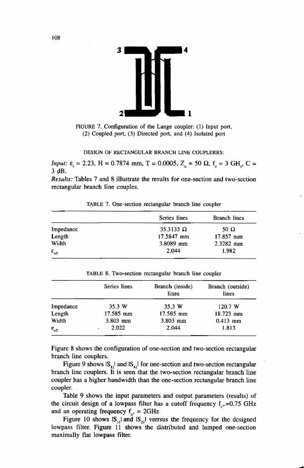
Figure 8 shows the configuration of one-section and two-section rectangular branch line couplers.
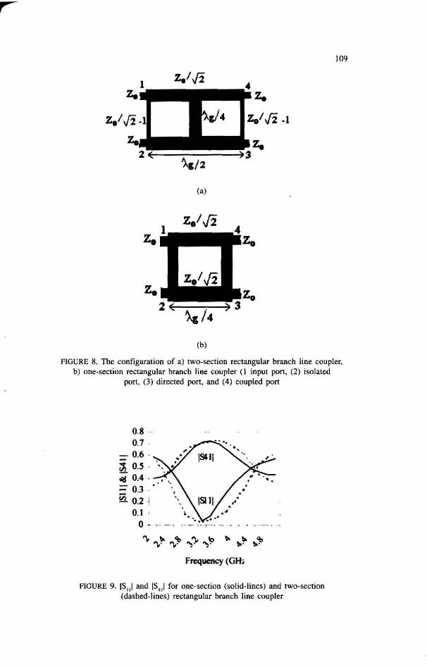
Figure 9 shows IS 11 1 and IS'11 for one-section and two-section rectangular branch line couplers. It is seen that the two-section rectangular branch line coupler has a higher bandwidth than the one-section rectangular branch line coupler.
Table 9 shows the input parameters and output parameters (results) of the circuit design of a lowpass filter has a cutoff frequency f, •. =O.75 GHz and an operating frequency f,. = 2GHz
Figure JO shows IS 111 and IS'11 verrsus the frequency for the designed lowpass filter. Figure 11 shows the distributed and lumped one-section maximally nat lowpass filter.
109
(a)
(b)
FJGURE 8. The configuration of a) two-section rectangular branch line coupler, b) one-section rectangular branch line coupler (1 input port, (2) isolated
port, (3) directed port, and (4) coupled port
0.8 · 0.7 . = 0.6 ·
~ O.S · <11$ 0.4 · = 0.3 . • iii 0.2 j
0.1 '
...... ~ ... " ..,"'..,'9 ~ ~~ ~" Frequency (GH,
FIGURE 9. IS .. I and IS411 for one-section (solid-Hnes) and two-section (dashed-lines) rectangular branch line coupler

110
TABLE 9. Input and output parameters of the 0.75 cutoff frequency lowpass filter
Input parameters
The substrate parameters with 50 Q
normalized impedance are: E, = 2.2 H = 0.7874 mm. and T = 0.005 mm. The operating frequency fo = 2 GHz, The cut-off frequency f, = 0.75 GHz. series conductance = 90 n. The characteristic impedance of the shunt capacitance = 20 n. One section maximally flat lowpass filter is considred.
Output parameters (results)
Length and width of the inductive microstrip line are 23.52 mm and 0.8321 mm, respectively. Length and width of the capacitive microstrip line are 29.94 nun and The lumped inductance and capacitance of the designed LPF are 0.4579x IO·"H. and 0.7132 x lO·J! F, respectively.
CURRENT PROGRAM VERSUS OTHER AVAILABLE PROGRAMS
To the best of our knowledge. the available microstrip design programs perform design of microstrip circuits with lengths and widths in a non
... , '" olj
'"
0.8
0.6
0.4
0.2
0
",":- "'~ ",":- , ,":> ,~ ,"?o
Frequency (GHz)
FIGURE to. ISul and IS211 versus the frequency for the designed lowpass filter
FIGURE 11. Schematic of the designed distributed lowpass filter and the corresponding lumped circuit.
...

r
III
suitable fonnat, such as applying the lengths in radians or electrical lengths but not in the actual lengths that are usually needed for manufacturing or analyzing the circuit. In addition, some of these programs are so expensive, others do not consider full microstrip discontinuities and do not cover a wide range of micros trip circuit design applications.
Compared to these programs, our HHSS2-program enjoys the following advantages: I. It covers a wide range of applications in the design of passive and active
linear micros trip circuits. 2. It considers the microstrip discontinuities. 3. It can be used to perform a complete design of microstrip devices such
as a complete mixer design with hybrid couplers, matching circuit, and IF filters.
4. It can be used to perfonn complete design of a micros trip system such as a receiver that cantains local oscillator, RF amplifier, and signal mixer and a transmitter that contains a power combiner besides RF oscillator and amplifiers.
5. The program perfonns design of)., IS-and 3)" IS- matching circuits with • • different microstrip widths. or 50-Q microstrip lines of different lengths as upon the user choice.
6. It presents the micros trip lengths in different fonnat such as radian, normalized lengths or actual lengths or actual lengths that can be used for many circuit analysis packages such as CiNL2 (Artech House 1994), MCAP, modified MCAP, etc.
7. The program is an easy DOS-based user-oriented program with a 150-Kbytes memory size, and thus can be used in XT, or AT PC computers.
S. The program can be attached with a grapher through the output text file to draw the circuit configiration.
9. The output data are formatted and stored in an output file for each application.
10. The program can be modified for used in the design of nonlinear microwave circuits. It can also be modified to draw the circuit configuration for each application. These two modifications will be the subject of a future publication.
CONCLUSIONS
This paper illustrates the general description of a user-oriented program called HHSS2 for microstrip circuit design. The program is used for passive microwave circuit design such as directional couplers (especially circularl rectangular branch-line couplers) and maximally flat or Chebyshev lowpass filters. The program is used also for the design of linear microwave acti ve circuits such as amplifiers, oscillators, and mixer. The program can also be used for stability change from unconditional stability to potential unstability and vise versa by connecting a series feedback stub with a certain length or connecting a cascaded resistor to the transistor terminals. The matching circuit obtained by the program is accurately calculated without using Smith chart either by using stub lines of given Zo with different lengths or 19/5 (3lg/S) stub lines with different characteristic impedance.

APPENDIX 1. The main architecture of the software
Substrate parameters, tr, H, T, Zo Transistor S~parameters
Operating conditions
... ... ... ... ... ... Amplifier Oscillator· Mixer LPF Couplers Other
Circuit Circuit Circuit Circui t Ci rc uit Features Design Design Design Design Design
.l. .l. .l. .l. .l. .l. 2) Stability Circles, I ) Stabi lity Circles, 2) Diode Mixer I) M"imally n at I) Coupled-lines 2) Transistor IS)
K a nd Ll K and Ll Circuit Design Low-Pass Filter Couplers parameters with a 3) Unilateral Figure 2) Feed Back Circuit using Hyperbolic 2) Chebeshev 2) Branch-line cascaded resistor
of Menl 3) Linear Design Mean Tech. Low-Pass Filtcr Couplers 3) Analytical 4) Simultaneous approach 3) Diode Mixer 3) Ring Couplers matching circuit
conjugate match 4) Quasi-linear Circuit Design 4) Wilkinson design for a g iven 5) Noise Figure Design approach using Diode Couplers z.
Circles 5) Analytical match Equivalent Circuit 5) Lange Couplers 4) Feedback circuit 6) Power and Circuits 4) Single and Dual design
Available gain gales mixer 5) Conversion Circles Circuit Design between rand Z
7) Input and Output 6) Edr \ and width Reneetion ca lculation for Coefficients given Zo and Co
8) Analytical matching Circuits
l

r
113
APPENDIX 2: A Sample of an Output Data File Data.DAT
The sample illustrates the output data file for the matching circuit design. It is seen that the length of the microstrip lines are given in actual lengths. normalized lengths, and in radians. In addition, the stub lengths are given in actual lengths, normalized lengths, radians, and as equivalent susceptances. It is also demonstrated that the software can perform analytical matching circuit design with 50·(microstrip lines with different lengths or with (g18, 3 (g18 lengths with different widths.
ANALYTICAL MATCHING CIRCUIT DESIGN
ALL LENGTHS ARE IN rum
MATCHING CIRCUIT CESIGN USING 50 OHM LINES WITH DIFFERENT LENGHTS ...... un
GAMMASMAG = .2915E+00 GAMMASMAG = .4227E+02 zs(normal.) = .1400E+OI .6000E+00 YS(normal) = .6034E+00 -.2586E+00 ZO = .5000E+02 LAMG = .7144E+02 WIDTH = .2302E+OI EFF = 1.982238 LENGTH OF SERIES LINE (for short stub) = 6.416701 LENGTH OF SERIES LINE (for open slub) = .2320E+02 EFF = 1.982238 LENGTH OF SHORT CIRCUIT BALANC STUB = 14.496100 LENGTH OF OPEN CIRCUIT BALANC STUB = 3.362906 LENGTH OF SHORT CIRCUIT SINGLE STUB = 11.636100 LENGTH OF OPEN CIRCUIT SINGLE STUB = 6.222911
NORMAL LENGTH OF SERIES LINE (for short stub) = 8.982442£-02 NORMAL LENGTH OF SERIES LINE (for open stub) = 2.927487E-OI NORMAL LENGTH OF SHORT CIRCUIT SALANC STUB = 2.029242E-Ol NORMAL LENGTH OF OPEN CIRCUIT BALANC STUB = 4.707576E-OI NORMAL LENGTH OF SHORT CIRCUIT SINGLE STUB = 1.628883E-Ol NORMAL LENGTH OF OPEN CIRCUIT SINGLE STUB = 8.711164E-02
RAD LENGTH OF SERIES LINE (for short stub) = 5.643835E-Ol RAD LENGTH SERIES LINE (open circuit) = 1.839394 RAD LENGTH OF SHORT CIRCUIT BALANC STUB = 1.275011 RAD LENGTH OF OPEN CIRCUIT BALANC STUB = 2.95785E-Ol RAD LENGTH OF SHORT CIRCUIT SINGLE STUB = 1.023458 RAD LENGTH OF OPEN CIRCUIT BALANC STUB = 5.473386E-Ol SUSCEP OF SHORT CIRCUIT BALANC STUB = 164.082500 SUSCEP OF OPEN CIRCUIT BALANC STUB = 6.094494E-03 SUSCEP OF SHORT CIRCUIT SINGLE STUB = 82.041270 SUSCEP OF OPEN CIRCUIT STUB = 1.218899E-02
MATCHING CIRCUIT DESIGN USING (I18)LAMG OR (3/8) LAMGA STUB
SERIES T.L ZO = 6437E+02 LAMG = 7232E+02 WID = .1546E+OI LENGTH = .1808+02 SHUNT STUB: LENGTH OF SHORT CIRCUIT SHUNT STUB = 9.462488 OR
Length OF OPEN CIRCUIT SHUNT STUB = 28.387460 FOR SINGLE STUB, ZO = 193.333300 WID = 7.804558E-02 FOR BALANCE STUB, ZO = 386.666600 WID = 1.379758E-03

114
REFERENCES
AI-Anwar, H. I., 1999. Computer-aided design of microwave planar six port reflection analyzer. M. Sc. Thesis, Faculty of Engineering, Ain-Shams University, Cairo, Egypt.
1994. C.NL2 2.0 Program for Windows. New York: Artech House Inc. Badaway. G. E. 1967. Two port power flow analysis using generalized scauering
parameters. Microwave Journal. Collin R. E., 1992. Foundation/or Microwave Engineering, 2fe. New York: McGraw
Hill Inc. Compact Software Inc. 2002. SUPER COMPACf, Paterson, N. 1.: Compact Software
Jnc. Dobrowolski J. A. 1991. Introduction to Computer Methods/or Microwave Circuit
Analysis and Design. New York: Artech House Inc. EEsof. Inc. 1997. TOUCHTONE. Westlake Village, WA. EI-Motaafy H.A., EI-Hannawy, EI-Badawy EI-S.A & Ibrahim S.H. 1995. A Complete
Computer Program for Micros/rip Circuit Design . Aug. 27-31. Istanbul. Turkey. EI-Motaafy H.A .. EI-Arabaty M.M. Ibrahim S.H. 1990. Design and Realization of
Microwave oscillator and Amplifiers Using Microstrip Technology. The XIII Conference on Solid-State Science. 20·26 January. Sohag-Qena. Egypt.
Encelbrechr. R. 1965. A wide-band low noise L-band balanced transistor amplifiers. IEEE Proc. 53: 237-247.
Fusco. V. F.. 1987. Microwave Circuits, Analysis and CompuTer·Aided Design. London: Prentise-Hall International Ltd.
Garg, R. & Bahl, I. J. 1979. Characteristic of coupled microstrip lines. IEEE Transaction, MIT- 27. No.7: 700-705.
Gentitle. C. 1987. Microwave Amplifier and Oscillators. New York: McGraw-Hill Book Company.
Gonzalez, G. 1997. Microwave Transistor Amplifiers Analysis and Design, 2/e. Englewood Cliffs Prentice-Hall. NJ, 1997.
Ha. T. T. J981 . Solid-Stafe Microwave Amplifiers DeSign. New York: John Wiley and Sons.
Hewlett Packard, Application Note 995. The Schottky Diode Mixers. Hewlett Packard, Application Note 963.1mpedallce Matching Techniques/or Mixers
and Detectors. Holzman, E. and Roberston R.. 1992. Solid-State Microwave Power Oscillator
Design. New York: Artech House Inc. Ibrahim, S. H., 2000. Computer aided design and analysis of 2-4 GHz brodband
balanced microstrip amplifier. Accepted for Publication in llUM~Engineering Journal, Kuala Lumpur. Malaysia, 1 (1) Jan 2000.
Lange. J ., 1969. Imerdigitated stripline quadrature hybrid. IEEE Trans. 17(11): 1150-1. .
Maas, S. A. 1986. Microwave Mixers. Norwood. Mass: Artech House Book. Osmani, R. M. 1981. Syntesis of Lange Couplers. IEEE Trans. 29(2): 186-70. Ou, W. P. 1975. Design equations for interdigitated direction couplers. IEEE Trans.
19 (2): 253-5. Stassiades, A. et al. 1992. Solid-STate Microwave Generators. Chapman & Hall.
EI-Sayed A. EI-Badawy Department of Electrical bngineering Faculty of Engineering, Alexandria University Alexandria 21544. Egypt
Saia H. Ibrahim Computer Science Department Faculty of Computer and Infannation Mansuora University Mansuora. Egypt
.. ___ ___ . __ . _____ J