Embed Size (px)
Citation preview
International Journal of Advances in Engineering & Technology, March 2012.
©IJAET ISSN: 2231-1963
161 Vol. 3, Issue 1, pp. 161-174
ANALYSIS AND COMPARISON OF COMBINATIONAL
CIRCUITS BY USING LOW POWER TECHNIQUES
Suparshya Babu Sukhavasi1, Susrutha Babu Sukhavasi
1, Vijaya Bhaskar M
2,
B Rajesh Kumar3
1Assistant Professor, Department of ECE, K L University, Guntur, AP, India.
2M.Tech -VLSI Student, Department of ECE, K L University, Guntur, AP, India.
3M.Tech-Embedded VLSI Student, Department of ECE, SITE, T P Gudam, AP, India.
ABSTRACT
Power dissipation is the major aspect which is effecting the digital circuits. By implementing the self resetting
logic to the digital circuit, the power dissipation is drastically reduced. In the VLSI Design this low power
technique is very advanced for DSP applications. The dynamic circuits are becoming increasingly popular
because of the speed advantage over static CMOS logic circuits; hence they are widely used today in high
performance and low power circuits. Self-resetting logic is a commonly used piece of circuitry that can be found
in use with memory arrays as word line drivers. Self resetting logic implemented in dynamic logic families have
been proposed as viable clock less alternatives. The combinational logic is a type of digital logic which is
implemented by Boolean circuits, where the output is a pure function of the present input only. This is in
contrast to sequential logic, in which the output depends not only on the present input but also on the history of
the input. In this paper mainly the self resetting logic is applied for the different combinational circuits and the
analysis is done very clearly. By implementing this low power technique for different logic circuits and adders,
by comparison with DYNAMIC and SRCMOS logic’s power dissipation is drastically reduced up to 35%
compared with CMOS logic circuits and observations are tabulated.
KEYWORDS: High speed, VLSI, Self-resetting logic (SRL), topologies, power dissipation
I. INTRODUCTION
Combinational logic is used in computer circuits to do Boolean algebra on input signals and on stored
data. Practical computer circuits normally contain a mixture of combinational and sequential logic.
The part of an arithmetic logic unit, or ALU, that does mathematical calculations is constructed using
combinational logic. Other circuits used in computers, such as half adders, full adders, half
subtractors, full subtractors, multiplexers, demultiplexers, encoders and decoders are also made by
using combinational logic.
In today‘s fast processing environment, the use of dynamic circuits is becoming increasingly popular
[5]. Dynamic CMOS circuits are defined as those circuits which have an additional clock signal inputs
along with the default combinational circuit inputs of the static systems. Dynamic systems are faster
and efficient than the static systems. A fundamental difficulty with dynamic circuits is the
monotonicity requirement. In the design of dynamic logic circuits numerous difficulties may arise like
charge sharing, feed through, charge leakage, single-event upsets, etc. In this paper novel energy-
efficient self-resetting primitive gates followed by the design of adder logic circuits are proposed.
Addition is a fundamental arithmetic operation that is generally used in many VLSI systems, such as
application-specific digital signal processing (DSP) architectures and microprocessors [2]. This
module is the core of many arithmetic operations such as addition/subtraction, multiplication, division
and address generation. Such high performance devices need low power and area efficient adder
International Journal of Advances in Engineering & Technology, March 2012.
©IJAET ISSN: 2231-1963
162 Vol. 3, Issue 1, pp. 161-174
circuits. So this paper presents a design construction for primitive gates and adder circuits which
reduce delay and clock skew when compared to the dynamic logic adder implementation [9].
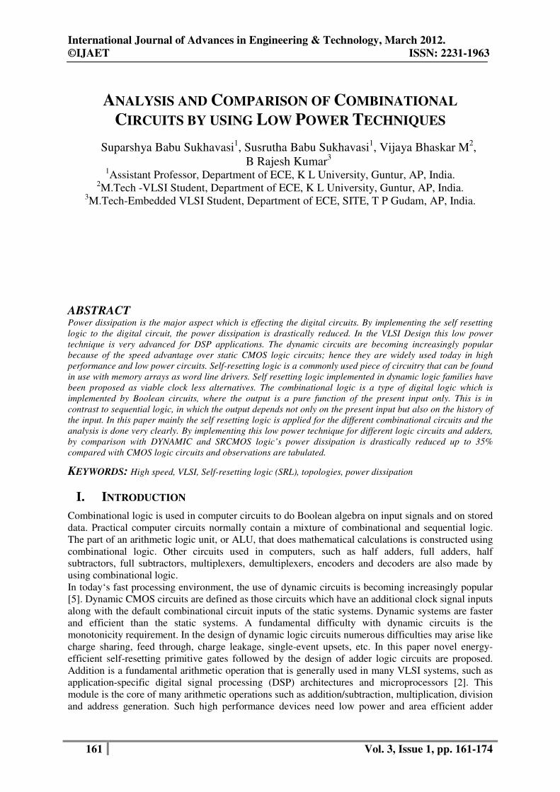
Fig.1. Basic Structure of A Self Resetting Logic Circuit
Another category of dynamic circuits, called self-resetting CMOS (SRCMOS), represents signals as
short-duration pulses rather than as voltage levels. When a set of pulses are sent to the inputs to a
logic gate, they must arrive at essentially the same time and they must overlap with one another for a
minimum duration. After a logic gate has processed a set of input pulses, a reset signal is activated
that restores the logic gate to a state in which it can receive another set of input pulses. The reset
operation is timed to occur after the input pulses have returned to zero [11]. Thus, there is no need for
an evaluate or “foot” transistor since the pull-down network will be off during the reset operation, and
this is one of the factors that leads to high-speed operation. Moreover, since the reset occurs
immediately after each gate has evaluated, there is no need for a separate precharge phase. Since
short-duration pulses are hard to debug and test, special additional test-mode features are sometimes
added for these purposes. Two types of reset structures have been proposed for use in SRCMOS. In
globally self-resetting CMOS [4], the reset signal for each stage is generated by a separate timing
chain which provides a parallel worst-case delay path. Individual reset signals are obtained at various
tap points along this timing chain in such a way that the reset pulse arrives at each stage only after the
stage has completed its evaluation.
Very careful device sizing based on extensive simulations over process-voltage-temperature corners
are required in order to ensure correct operation. Moreover, any extra delay margin that is designed
into the timing chain simply reduces the throughput by a corresponding amount. On the other hand, in
locally self-resetting CMOS [5], the reset signal for each stage is generated by a mechanism local to
that stage. Previous implementations of this technique have been based on single-rail domino stages in
which the reset signal is obtained by sending the stage’s own output signal through a short delay
chain. Again, this technique requires very careful simulations and device sizing in order to ensure that
the reset signals do not arrive too early. As with the other technique, any timing margin that is built in
will directly limit the achievable performance.
II. SELF RESETTING CMOS DYNAMIC LOGIC
Self-resetting logic is a commonly used piece of circuitry that automatically precharge they (i.e., reset
themselves) after a prescribed delay. They find applications where a small percentage of gates switch
in a cycle, such as memory decoder circuits. It is a form of logic in which the signal being propagated
is buffered and used as the precharge or reset signal. By using a buffered form of the input, the input
loading is kept almost as low as in normal dynamic logic while local generation of the reset assures
that it is properly timed and only occurs when needed [6].
A generic view of a self-reset logic is shown in Fig.1. In the domino case, the clock is used to operate
the circuit. In the self-resetting case, the output is fed back to the precharge control input and, after a
specified time delay, the pull-up is reactivated. There is an NMOS sub block where the logic function
performed by the gate is implemented which is represented as NMOS_LF through which the input
Nfet
logic Inputs
Cx
Vx Cout Vout
VDD VSGR Delay chain
International Journal of Advances in Engineering & Technology, March 2012.
©IJAET ISSN: 2231-1963
163 Vol. 3, Issue 1, pp. 161-174
data‘s are loaded. The output of the gate F provides a pulse if the logic function becomes true. This
output is buffered and it is connected to PMOS structure to precharge [7]. The delay line is
implemented as a series of inverters. The signals that propagate through these circuits are pulses.
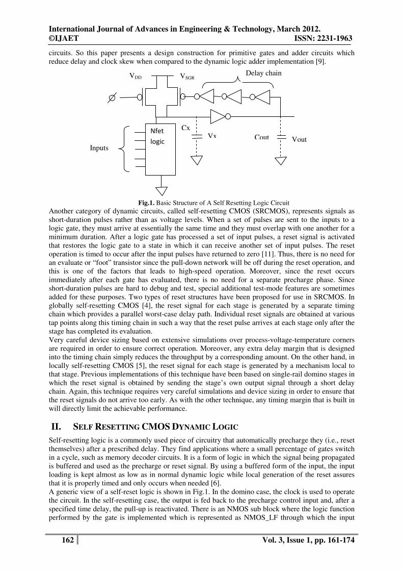
Fig.2. Precharge
Dynamic logic circuits are widely used in modern low power VLSI circuits. These dynamic circuits
are becoming increasingly popular because of the speed advantage over static CMOS logic circuits;
hence they are widely used today in high performance and low power circuits. Normally in the design
of flip-flops and registers, the clock distribution grid and routing to dynamic gates presents a problem
to CAD tools and introduces issues of delay and skew into the circuit design process [1]. There are
situations that permit the use of circuits that can be automatically precharge themselves (i.e., reset
themselves) after a prescribed delays [7]. These circuits are called post charge or self-resetting logic
which are widely used in memory decoders.
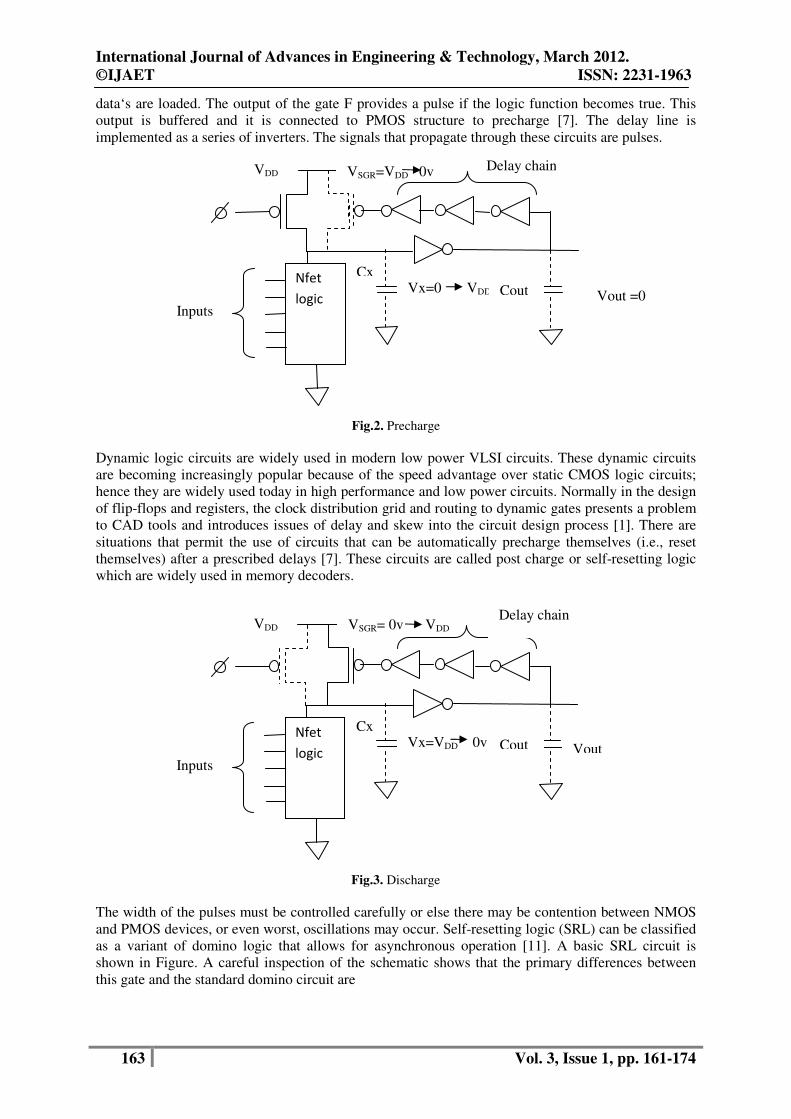
Fig.3. Discharge
The width of the pulses must be controlled carefully or else there may be contention between NMOS
and PMOS devices, or even worst, oscillations may occur. Self-resetting logic (SRL) can be classified
as a variant of domino logic that allows for asynchronous operation [11]. A basic SRL circuit is
shown in Figure. A careful inspection of the schematic shows that the primary differences between
this gate and the standard domino circuit are
Nfet
logic Inputs
Cx
Vx=VDD 0v Cout Vout
VDD VSGR= 0v VDD Delay chain
Nfet
logic Inputs
Cx
Vx=0 VDD Cout
VDD VSGR=VDD 0v Delay chain
Vout =0
International Journal of Advances in Engineering & Technology, March 2012.
©IJAET ISSN: 2231-1963
164 Vol. 3, Issue 1, pp. 161-174
(a) The addition of the inverter chain that provides feedback from the output voltage Vout (t) to
the gate of the reset pFET MR, and
(b) The elimination of the evaluation nFET.
Note that an odd number of inverters are used in the feedback. As discussed below, the feedback loop
has a significant effect on both the internal operation of the circuit and the characteristics of the output
voltage. Precharging of Cx occurs when the clock is at a value Ф=0 and the circuit conditions are
shown in Figure 2. During this time, and which is identical to the event in a standard domino circuit.
As we will see, the timing of the input signals precludes the possibility of a DC discharge path to
ground by insuring that the inputs to all logic nFET are 0 during precharge. The voltage on the gate of
MR is at a value of so that insures that MR is in cutoff during this time. The distinct features of SRL
arise when a discharge occurs. The circuit conditions are shown in Fig.3
III. ANALYSIS OF LOGIC GATES AND ADDERS
This section presents the basic construction and simulation of primitive gates and adders in all the
specified logics above they are DYNAMIC LOGIC, SRCMOS LOGIC, and SELF RESETTING
LOGIC. The cells shown in Fig. is a self-resetting implementation of 2-input primitive gates. The
logical functions are implemented by the NMOS stack with two input signals A and B. The delay path
in this circuit is implemented with single inverter. The mechanism of self-resetting in this circuit is
achieved through the PMOS transistors. The implementation of AND/OR can be obtained by placing
the NMOS stack in series and parallel connection, whereas the gates NAND/NOR can be
implemented with De Morgan‘s law, an OR gate with inverted input signals behaves as a NAND gate.
Similarly an AND gate with inverted input signals behaves as a NOR gate [8].
3.1 Dynamic logic implementation in logic gates and adders Dynamic logic is one of the low power technique which is applicable for digital circuits, in which the
area will be reduced where as the power reduction is less compared to Self resetting logic. Analysis of
basic logic gates and their applications is done.
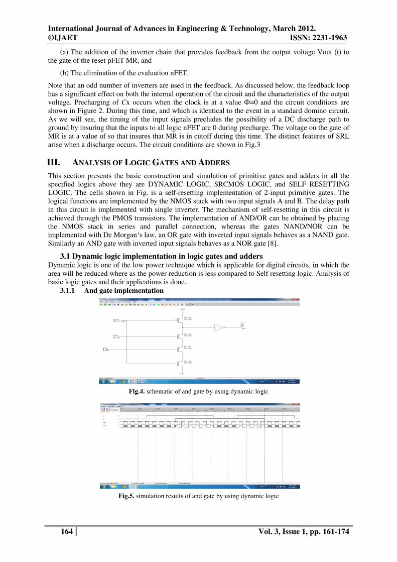
3.1.1 And gate implementation
Fig.4. schematic of and gate by using dynamic logic
Fig.5. simulation results of and gate by using dynamic logic
International Journal of Advances in Engineering & Technology, March 2012.
©IJAET ISSN: 2231-1963
165 Vol. 3, Issue 1, pp. 161-174
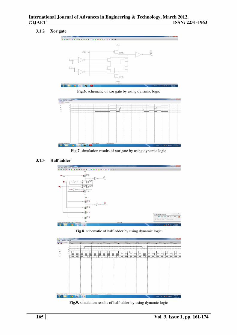
3.1.2 Xor gate
Fig.6. schematic of xor gate by using dynamic logic
Fig.7. simulation results of xor gate by using dynamic logic
3.1.3 Half adder
Fig.8. schematic of half adder by using dynamic logic
Fig.9. simulation results of half adder by using dynamic logic
International Journal of Advances in Engineering & Technology, March 2012.
©IJAET ISSN: 2231-1963
166 Vol. 3, Issue 1, pp. 161-174
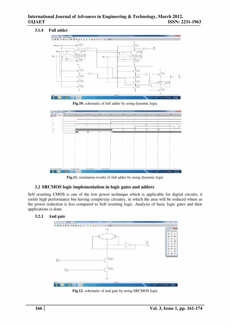
3.1.4 Full adder
Fig.10. schematic of full adder by using dynamic logic
Fig.11. simulation results of full adder by using dynamic logic
3.2 SRCMOS logic implementation in logic gates and adders
Self resetting CMOS is one of the low power technique which is applicable for digital circuits, it
yields high performance but having complexity circuitry, in which the area will be reduced where as
the power reduction is less compared to Self resetting logic. Analysis of basic logic gates and their
applications is done.
3.2.1 And gate
Fig.12. schematic of and gate by using SRCMOS logic
International Journal of Advances in Engineering & Technology, March 2012.
©IJAET ISSN: 2231-1963
167 Vol. 3, Issue 1, pp. 161-174
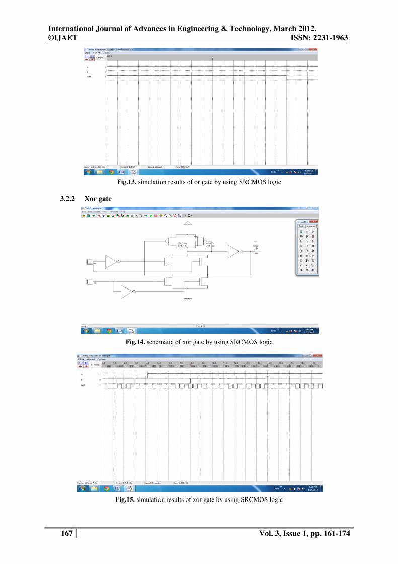
Fig.13. simulation results of or gate by using SRCMOS logic
3.2.2 Xor gate
Fig.14. schematic of xor gate by using SRCMOS logic
Fig.15. simulation results of xor gate by using SRCMOS logic
International Journal of Advances in Engineering & Technology, March 2012.
©IJAET ISSN: 2231-1963
168 Vol. 3, Issue 1, pp. 161-174
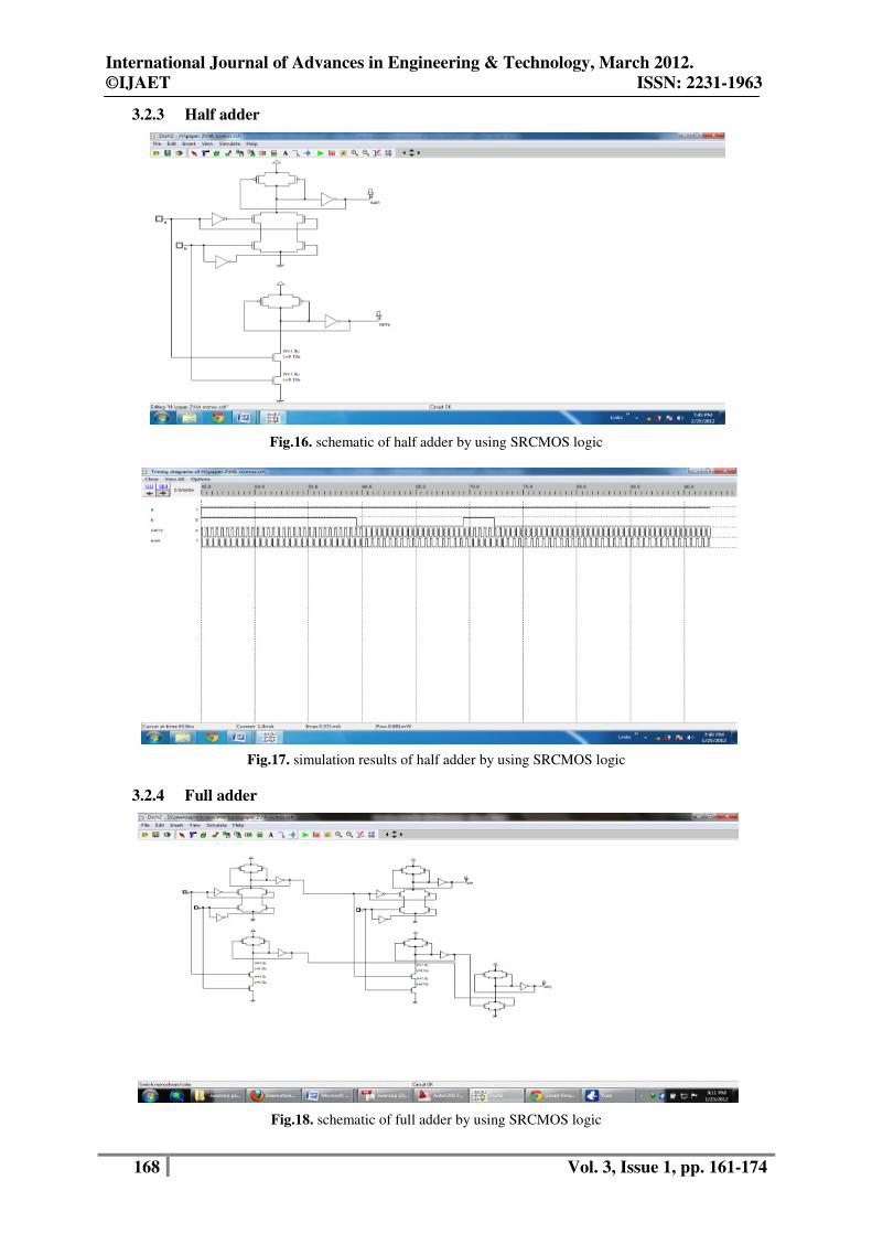
3.2.3 Half adder
Fig.16. schematic of half adder by using SRCMOS logic
Fig.17. simulation results of half adder by using SRCMOS logic
3.2.4 Full adder
Fig.18. schematic of full adder by using SRCMOS logic
International Journal of Advances in Engineering & Technology, March 2012.
©IJAET ISSN: 2231-1963
169 Vol. 3, Issue 1, pp. 161-174
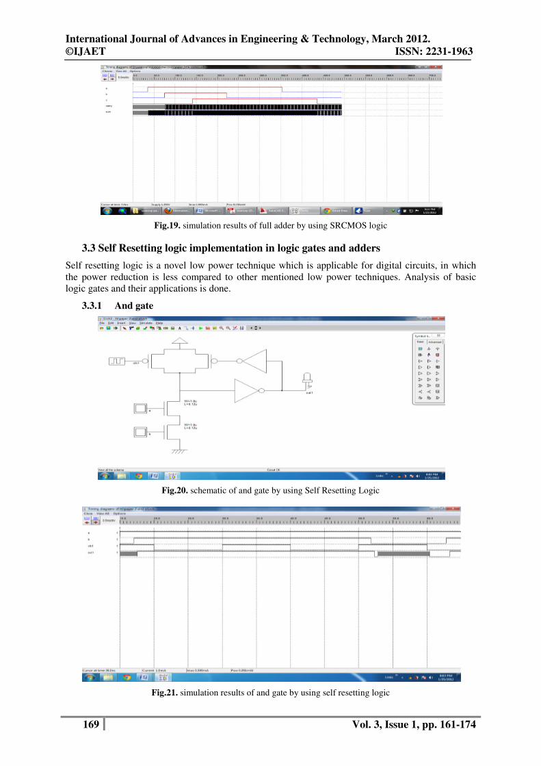
Fig.19. simulation results of full adder by using SRCMOS logic
3.3 Self Resetting logic implementation in logic gates and adders
Self resetting logic is a novel low power technique which is applicable for digital circuits, in which
the power reduction is less compared to other mentioned low power techniques. Analysis of basic
logic gates and their applications is done.
3.3.1 And gate
Fig.20. schematic of and gate by using Self Resetting Logic
Fig.21. simulation results of and gate by using self resetting logic
International Journal of Advances in Engineering & Technology, March 2012.
©IJAET ISSN: 2231-1963
170 Vol. 3, Issue 1, pp. 161-174
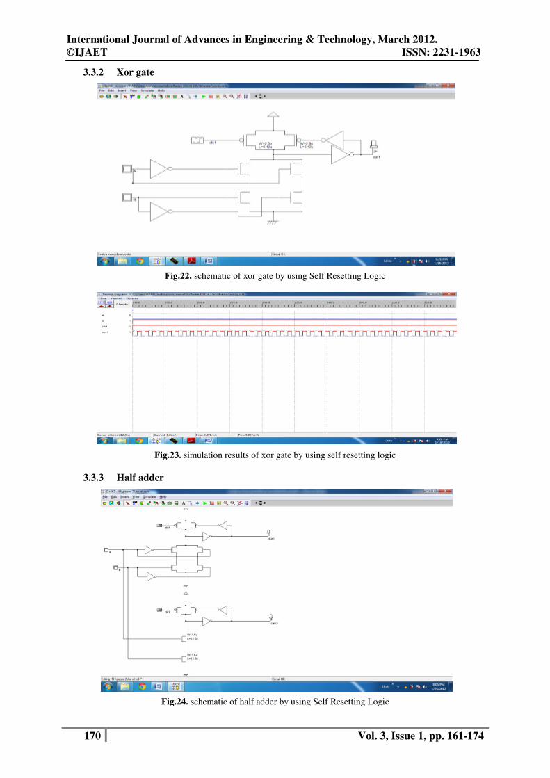
3.3.2 Xor gate
Fig.22. schematic of xor gate by using Self Resetting Logic
Fig.23. simulation results of xor gate by using self resetting logic
3.3.3 Half adder
Fig.24. schematic of half adder by using Self Resetting Logic
International Journal of Advances in Engineering & Technology, March 2012.
©IJAET ISSN: 2231-1963
171 Vol. 3, Issue 1, pp. 161-174
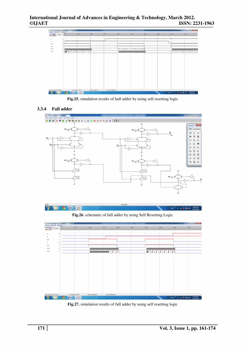
Fig.25. simulation results of half adder by using self resetting logic
3.3.4 Full adder
Fig.26. schematic of full adder by using Self Resetting Logic
Fig.27. simulation results of full adder by using self resetting logic
International Journal of Advances in Engineering & Technology, March 2012.
©IJAET ISSN: 2231-1963
172 Vol. 3, Issue 1, pp. 161-174
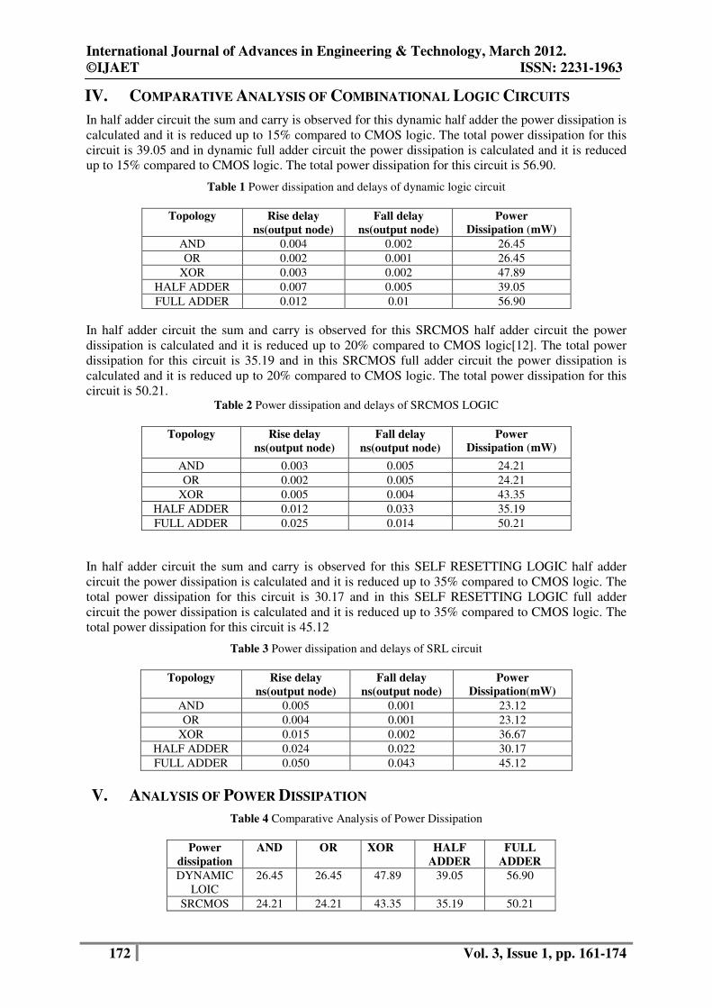
IV. COMPARATIVE ANALYSIS OF COMBINATIONAL LOGIC CIRCUITS
In half adder circuit the sum and carry is observed for this dynamic half adder the power dissipation is
calculated and it is reduced up to 15% compared to CMOS logic. The total power dissipation for this
circuit is 39.05 and in dynamic full adder circuit the power dissipation is calculated and it is reduced
up to 15% compared to CMOS logic. The total power dissipation for this circuit is 56.90.
Table 1 Power dissipation and delays of dynamic logic circuit
Topology Rise delay
ns(output node)
Fall delay
ns(output node)
Power
Dissipation (mW)
AND 0.004 0.002 26.45
OR 0.002 0.001 26.45
XOR 0.003 0.002 47.89
HALF ADDER 0.007 0.005 39.05
FULL ADDER 0.012 0.01 56.90
In half adder circuit the sum and carry is observed for this SRCMOS half adder circuit the power
dissipation is calculated and it is reduced up to 20% compared to CMOS logic[12]. The total power
dissipation for this circuit is 35.19 and in this SRCMOS full adder circuit the power dissipation is
calculated and it is reduced up to 20% compared to CMOS logic. The total power dissipation for this
circuit is 50.21. Table 2 Power dissipation and delays of SRCMOS LOGIC
Topology Rise delay
ns(output node)
Fall delay
ns(output node)
Power Dissipation (mW)
AND 0.003 0.005 24.21
OR 0.002 0.005 24.21
XOR 0.005 0.004 43.35
HALF ADDER 0.012 0.033 35.19
FULL ADDER 0.025 0.014 50.21
In half adder circuit the sum and carry is observed for this SELF RESETTING LOGIC half adder
circuit the power dissipation is calculated and it is reduced up to 35% compared to CMOS logic. The
total power dissipation for this circuit is 30.17 and in this SELF RESETTING LOGIC full adder
circuit the power dissipation is calculated and it is reduced up to 35% compared to CMOS logic. The
total power dissipation for this circuit is 45.12
Table 3 Power dissipation and delays of SRL circuit
Topology Rise delay
ns(output node)
Fall delay
ns(output node)
Power Dissipation(mW)
AND 0.005 0.001 23.12
OR 0.004 0.001 23.12
XOR 0.015 0.002 36.67
HALF ADDER 0.024 0.022 30.17
FULL ADDER 0.050 0.043 45.12
V. ANALYSIS OF POWER DISSIPATION
Table 4 Comparative Analysis of Power Dissipation
Power
dissipation
AND OR XOR HALF
ADDER
FULL
ADDER
DYNAMIC
LOIC
26.45 26.45 47.89 39.05 56.90
SRCMOS 24.21 24.21 43.35 35.19 50.21

International Journal of Advances in Engineering & Technology, March 2012.
©IJAET ISSN: 2231-1963
173 Vol. 3, Issue 1, pp. 161-174
LOGIC
SRL 23.12 23.12 36.67 30.17 45.12
Chart 1 analysis of power dissipation
IV. CONCLUSION
In this paper, an exhaustive analysis for commonly used high-speed primitive gates and adder circuits
using self-resetting logic is implemented in 45-nm CMOS technologies. The goal was to obtain a
family of gates that could simplify the implementation of fast processing circuit which overcomes the
restriction due the pulses being elongated and shortened as signal traverse the logic stages. In this
paper exhaustive comparison between conventional DYNAMIC LOGIC, SRCMOS and SRL were
carried in terms of its parasitic value, delays and power dissipation. It is observed that the proposed
circuits have offered an improved performance in power dissipation, charge leakage and clock skew
when compared to DYNAMIC LOGIC and SRCMOS logic with additional burden of silicon area.
Hence, it is concluded that the proposed designs will provide a platform for designing high
performance and low power digital circuits and high noise immune digital circuits such as, digital
signal processors and multiplexers.
REFERENCES
[1] Woo Jin Kim, Yong-Bin Kim, ―A Localized Self-Resetting Gate Design Methodology for Low Powerǁ
IEEE 2001.
[2] M. E. Litvin and S. Mourad, ―Self-reset logic for fast arithmetic applications,ǁ IEEE Transactions on Very
Large Scale Integration Systems, vol. 13, no. 4, pp. 462–475, 2005.
[3] L. Wentai, C. T. Gray, D. Fan, W. J. Farlow, T. A. Hughes, and R. K. Cavin, ―250-MHz wave pipelined
adder in 2-µm CMOS,ǁ IEEE Journal of Solid-State Circuits, vol. 29, no. 9, pp. 1117–1128, 1994.
[4] D. Patel, P. G. Parate, P. S. Patil, and S. Subbaraman, ―ASIC implementation of 1-bit full adder,ǁ in Proc.
1st Int. Conf. Emerging TrendsEng. Technol., Jul. 2008, pp. 463–467.
[5] M. Lehman and N. Burla, ―Skip techniques for high-speed carry Propagation in binary arithmetic units,ǁ
IRE Trans. Electron.comput., vol. EC-10, pp. 691–698, Dec. 1962.
[6] R. A. Haring, M.S. Milshtein, T.I. Chappell, S. H. Dong and B.A. Chapell, "Self resseting logic and
incrementer" in Proc. IEEE Int. Symp. VLSI Circuits, 1996 pp. 18-19.
[7] G. Yee and C. Sechen, " Clock-delayed domino for adder and combinational logic design" in
proc.IEEE/ACM Int. Conf. Computer Design, Oct., 1996, pp. 332-337.
[8] P. Ng, P. T. Balsara, and D. Steiss, ―Performance of CMOS Differential Circuits,ǁ IEEE J. of Solid-State
Circuits, vol. 31, no. 6, pp. 841-846, June 1996.
[9] P. Srivastava, A. Pua, and L. Welch, .Issues in the Design of Domino Logic Circuits, Proceedings of the
IEEE Great Lakes Symposium on VLSI, pp. 108-112, February 1998.
[10] W. Zhao and Y. Cao. ―New generation of predictive technology model for sub-45nm design exploration,ǁ
In IEEE Intl. Symp. On Quality Electronics Design, 2006
[11] CMOS Logic Circuit Design 2002 John P Uyemura
[12] Prabhakara C. Balla and Andreas Antoniou― Low Power Dissipation MOS Ternary Logic FamilyǁIEE
journal of solid state circuits, vol sc-19 no.5 October 1984
0
10
20
30
40
50
60
AND OR XOR HALF
ADDER
FULL
ADDER
DYNAMIC LOIC
SRCMOS LOGIC
SRL
International Journal of Advances in Engineering & Technology, March 2012.
©IJAET ISSN: 2231-1963
174 Vol. 3, Issue 1, pp. 161-174
Authors
Suparshya Babu Sukhavasi was born in A.P, India. He received the B.Tech degree
from JNTU, A.P, and M.Tech degree from SRM University, Chennai, Tamil Nadu,
India in 2008 and 2010 respectively. He worked as Assistant Professor in Electronics
Engineering in Bapatla Engineering College for academic year 2010-2011 and from
2011 to till date working in K L University . His research interests include antennas,
FPGA Implementation, Low Power Design and wireless communications.
Vijaya Bhaskar Madivada was born in A.P, India. He received the B.Tech degree
in Electronics & Communications Engineering from Jawaharlal Nehru
Technological University in 2010. Presently he is pursuing M.Tech VLSI Design in
KL University; His research interests include FPGA Implementation, Low Power
Design.
B Rajesh Kumar was born in Gudivada, Krishna (Dist.,), AP, India. He received
B.Tech. in Electronics & Communications Engineering from Jawaharlal Nehru
Technological University in 2010 , A.P, India. Presently he is pursuing M.Tech. in
VLSI from SITE. His research interest includes Low Power and design of VLSI
circuits.
Susrutha Babu Sukhavasi was born in A.P, India. He received the B.Tech degree
from JNTU, A.P, and M.Tech degree from SRM University, Chennai, Tamil Nadu,
India in 2008 and 2010 respectively. He worked as Assistant Professor in Electronics
Engineering in Bapatla Engineering College for academic year 2010-2011 and from
2011 to till date working in K L University . His research interests include antennas,
FPGA Implementation, Low Power Design and wireless communications.