Embed Size (px)
Citation preview

Ripple Carry Adder 1
Section 1
INTRODUCTION
Ripple Carry Adder 2
The purpose of this project is to get familiarize us with design aspects of CMOS which is being used in the industry for the last decade. The main specification of the project is to design a binary 4 bit adder. We design the required adder starting from logic gate level, go up to form the circuit level & then draw the layout. The required integrity & specifications of the circuit can be checked by simulation data to the circuit & to the required output. Design of digital systems remains a very interesting & challenging field especially during the last decade. With the development of various kind of design & simulation tools the field is becoming more & more challenging & explore new ways of innovations.
Ripple Carry Adder 3
1.1 Given Task The given task is to: Design 4 bit Binary Full Adder Input two 4 bit numbers A & B. Output is 4 bit Sum and a Carry. We are allowed to use any adder form, CRA, CLA and any logic form static, dynamic or variation of these or within these families. Optimize Performance Measure Area (A), Time (T), Power (P) or AT2 are optimizing performance factors. We are given flexibility to choose anyone of these to optimize our design. Noise Margins: The noise margins should be at least 10% of the voltage swing. Rise and Fall times: All input signals and clocks have rise and fall times of less than 500 psec. The rise and fall times of the output signals (10% to 90%) should not exceed 500 psec. Load capacitance: Each output bit of the adder should have a 20 fF load. Simulation Simulation at every stage is required to check functionality and integrity of design. We are also required to re-simulate our extracted circuit after making layout. Layout Layout of only two gates of our design is required. And then we are allowed to use CADENCE library cell for more gates. We are to perform DRC on your final design, extract it and simulate it again to obtain our performance measures. Then we are to place and rout the complete chip including all I/O drivers and PADs. Give a complete specification for the circuit

Ripple Carry Adder 4
1.2 DESIGN SUMMARY
From given task we make our design philosophy based on parameters below: -
Adder Type We selected Ripple Carry Adder. Logic Form The static CMOS inverter has many excellent properties like fast speed, low power consumption and low sensitivity to noise and process variations. Our design is based on Static CMOS logic form. Goal of Optimization Adder is a speed-limiting element. The speed of the adder dominates the overall system performance. Thus, we chose Time (T) as optimizing performance factors. We will focus to optimize Carry Generation Delay. Optimization Techniques Different optimization techniques we use to achieve above goals are listed below: -
• Logic-level optimization • Transistor sizing • Progressive Transistor Sizing • Transistor ordering • Layout Consideration
Design Kit and process technology We use CMOSIS5 design kit from Canadian Microelectronics Corporation(CMC). The CMOSIS5 design kits is based on the Hewlett-Packard CMOS14TB process. This is a high-speed high density 0.5 micron CMOS process which feature a 0.6 micron drawn gate length optimized for 3.3V operation.
Ripple Carry Adder 5
Section 2
LOGIC DESIGN
Ripple Carry Adder 6
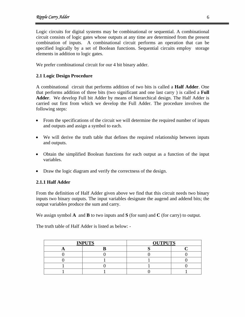
Logic circuits for digital systems may be combinational or sequential. A combinational circuit consists of logic gates whose outputs at any time are determined from the present combination of inputs. A combinational circuit performs an operation that can be specified logically by a set of Boolean functions. Sequential circuits employ storage elements in addition to logic gates. We prefer combinational circuit for our 4 bit binary adder. 2.1 Logic Design Procedure A combinational circuit that performs addition of two bits is called a Half Adder. One that performs addition of three bits (two significant and one last carry ) is called a Full Adder. We develop Full bit Adder by means of hierarchical design. The Half Adder is carried out first from which we develop the Full Adder. The procedure involves the following steps: • From the specifications of the circuit we will determine the required number of inputs
and outputs and assign a symbol to each. • We will derive the truth table that defines the required relationship between inputs
and outputs. • Obtain the simplified Boolean functions for each output as a function of the input
variables. • Draw the logic diagram and verify the correctness of the design. 2.1.1 Half Adder From the definition of Half Adder given above we find that this circuit needs two binary inputs two binary outputs. The input variables designate the augend and addend bits; the output variables produce the sum and carry. We assign symbol A and B to two inputs and S (for sum) and C (for carry) to output. The truth table of Half Adder is listed as below: -
INPUTS OUTPUTSA B S C 0 0 0 0 0 1 1 0 1 0 1 0 1 1 0 1
Ripple Carry Adder 7
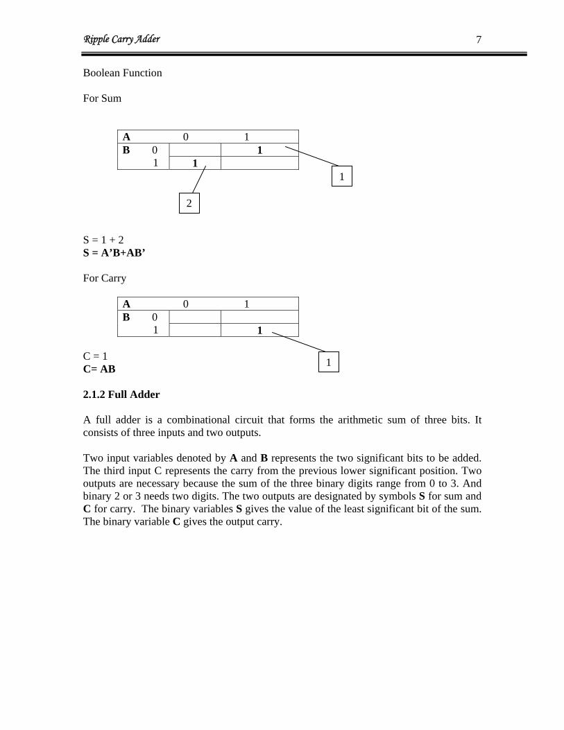
Boolean Function For Sum
A 0 1 1 B 0
1 1
2
1 S = 1 + 2 S = A’B+AB’ For Carry
A 0 1 B 0
1 1 C = 1 1C= AB 2.1.2 Full Adder A full adder is a combinational circuit that forms the arithmetic sum of three bits. It consists of three inputs and two outputs. Two input variables denoted by A and B represents the two significant bits to be added. The third input C represents the carry from the previous lower significant position. Two outputs are necessary because the sum of the three binary digits range from 0 to 3. And binary 2 or 3 needs two digits. The two outputs are designated by symbols S for sum and C for carry. The binary variables S gives the value of the least significant bit of the sum. The binary variable C gives the output carry.
Ripple Carry Adder 8
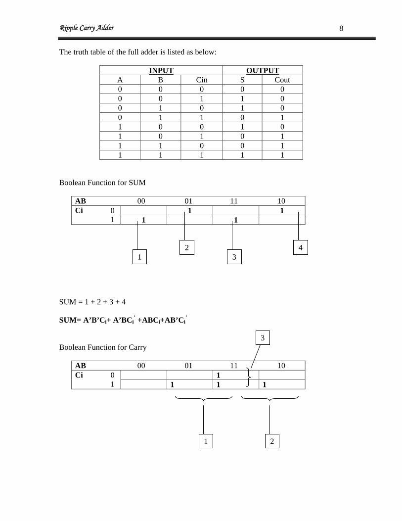
The truth table of the full adder is listed as below:
INPUT OUTPUTA B Cin S Cout 0 0 0 0 0 0 0 1 1 0 0 1 0 1 0 0 1 1 0 1 1 0 0 1 0 1 0 1 0 1 1 1 0 0 1 1 1 1 1 1
Boolean Function for SUM
AB 00 01 11 10 1 1 Ci 0
1 1 1 SUM = 1 + 2 + 3 + 4 SUM= A’B’Ci+ A’BCi
’ +ABCi+AB’Ci’
Boolean Function for Carry
AB 00 01 11 10 1 Ci 0
1 1 1 1
1 2
34
3
1 2
Ripple Carry Adder 9
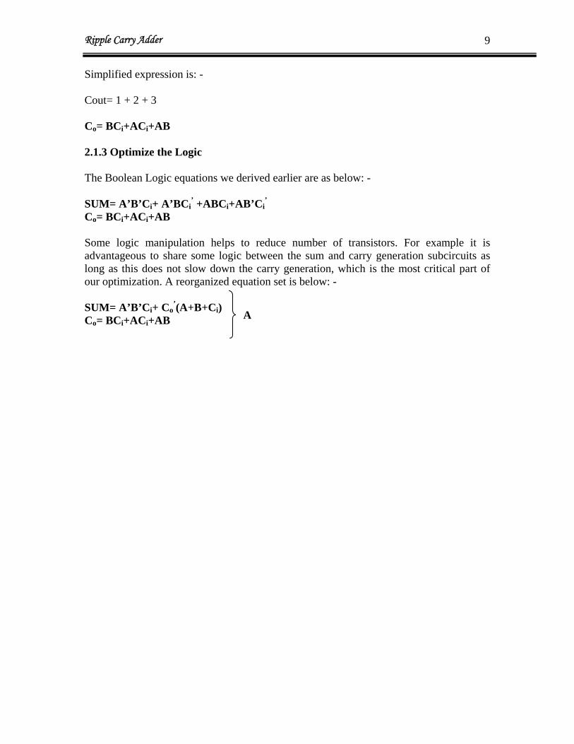
Simplified expression is: - Cout= 1 + 2 + 3
= BC +AC +AB Co i i 2.1.3 Optimize the Logic The Boolean Logic equations we derived earlier are as below: -
’ ’SUM= A’B’C + A’BC +ABC +AB’Ci i i iC = BC +AC +AB o i i Some logic manipulation helps to reduce number of transistors. For example it is advantageous to share some logic between the sum and carry generation subcircuits as long as this does not slow down the carry generation, which is the most critical part of our optimization. A reorganized equation set is below: -
A’SUM= A’B’C + C (A+B+C ) i o i
C = BC +AC +AB o i i
Ripple Carry Adder 10
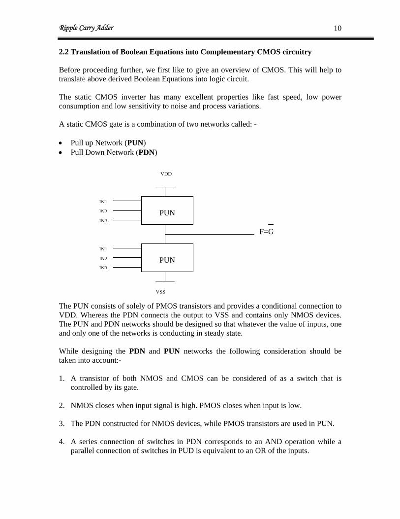
2.2 Translation of Boolean Equations into Complementary CMOS circuitry Before proceeding further, we first like to give an overview of CMOS. This will help to translate above derived Boolean Equations into logic circuit. The static CMOS inverter has many excellent properties like fast speed, low power consumption and low sensitivity to noise and process variations. A static CMOS gate is a combination of two networks called: - • Pull up Network (PUN) • Pull Down Network (PDN)
PUN
IN1
IN2
IN3
PUN
IN1
IN2
IN3
F=G
VDD
VSS
The PUN consists of solely of PMOS transistors and provides a conditional connection to VDD. Whereas the PDN connects the output to VSS and contains only NMOS devices. The PUN and PDN networks should be designed so that whatever the value of inputs, one and only one of the networks is conducting in steady state. While designing the PDN and PUN networks the following consideration should be taken into account:- 1. A transistor of both NMOS and CMOS can be considered of as a switch that is
controlled by its gate. 2. NMOS closes when input signal is high. PMOS closes when input is low. 3. The PDN constructed for NMOS devices, while PMOS transistors are used in PUN. 4. A series connection of switches in PDN corresponds to an AND operation while a
parallel connection of switches in PUD is equivalent to an OR of the inputs.
Ripple Carry Adder 11
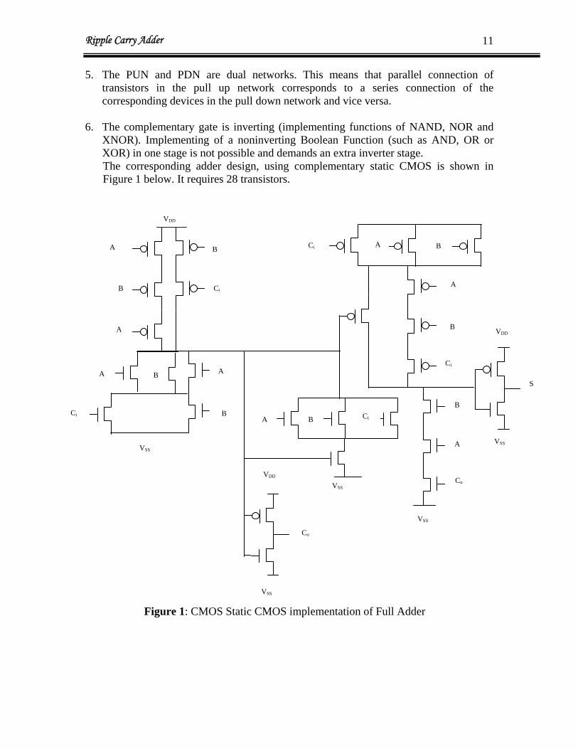
5. The PUN and PDN are dual networks. This means that parallel connection of transistors in the pull up network corresponds to a series connection of the corresponding devices in the pull down network and vice versa.
6. The complementary gate is inverting (implementing functions of NAND, NOR and
XNOR). Implementing of a noninverting Boolean Function (such as AND, OR or XOR) in one stage is not possible and demands an extra inverter stage. The corresponding adder design, using complementary static CMOS is shown in Figure 1 below. It requires 28 transistors.
S
VDD
VSS
VSSVSS
VDD
VSS
VDD
A
A
A
A
A B
B
B
A B
A B Ci
B
Ci
Co
B
Ci
Ci
A B
Ci
S
Co
VSS
Figure 1: CMOS Static CMOS implementation of Full Adder
Ripple Carry Adder 12
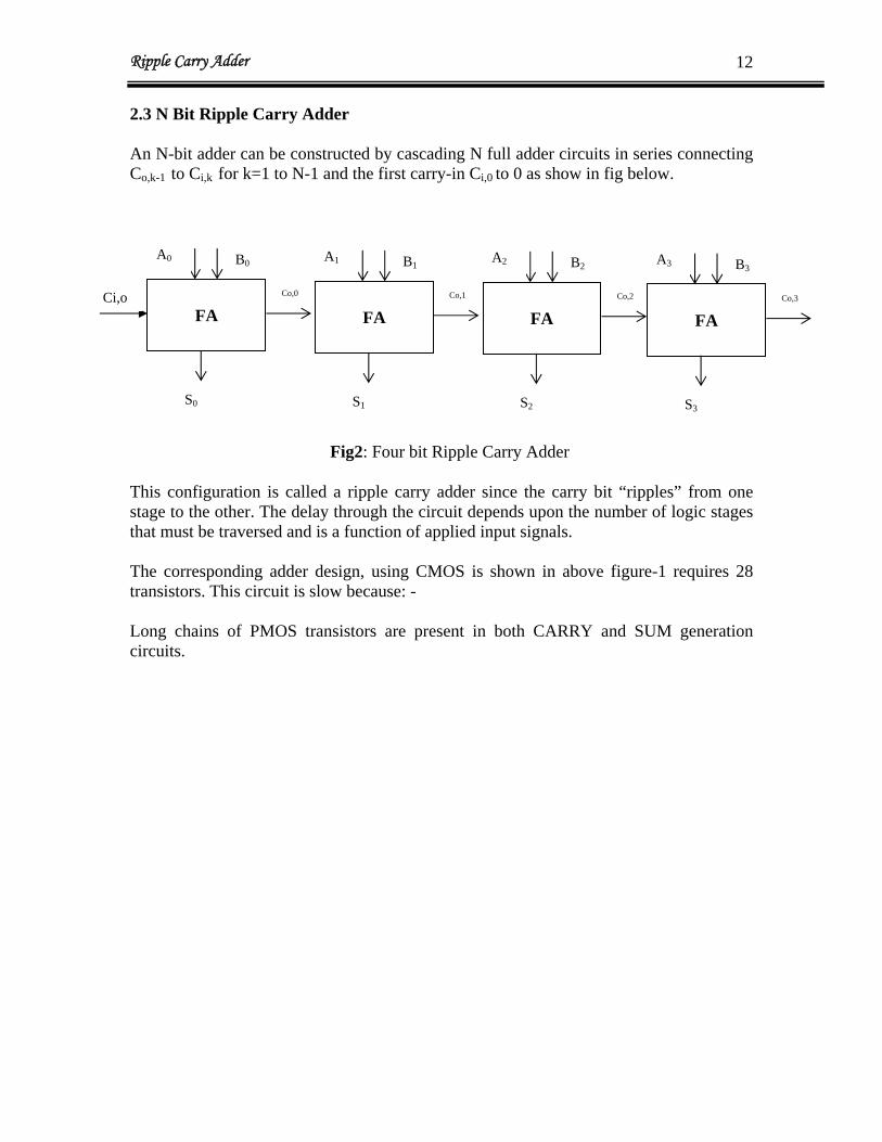
2.3 N Bit Ripple Carry Adder An N-bit adder can be constructed by cascading N full adder circuits in series connecting Co,k-1 to C for k=1 to N-1 and the first carry-in Ci,k i,0 to 0 as show in fig below.
FA
B0
S0
A0
Ci,o Co,0 FA
B1
S1
A1
Co,1 FA
B2
S2
A2
Co,2 FA
B3
S3
A3
Co,3
This configuration is called a ripple carry adder since the carry bit “ripples” from one stage to the other. The delay through the circuit depends upon the number of logic stages that must be traversed and is a function of applied input signals.
Fig2: Four bit Ripple Carry Adder
The corresponding adder design, using CMOS is shown in above figure-1 requires 28 transistors. This circuit is slow because: - Long chains of PMOS transistors are present in both CARRY and SUM generation circuits.
Ripple Carry Adder 13
Section 3
CIRCUIT OPTIMIZATION AND SIMULATION AT SCHEMATIC LEVEL
Ripple Carry Adder 14
3.1 Performance Evaluation of CMOS Ripple Carry Adder As our objective is to optimize the delay, we would remain committed to evaluate the performance of ripple carry adder with that respect. We determined in Ripple Carry Adder: - 1) The delay through the circuit depends upon the number of logic states that must be
traversed and is a function of the applied input signals. 2) The worse case delay happens when a carry generated at the last significant bit
position propagates all the way to the most significant bit. The delay is then proportional to the number of bits in the input word N and is approximated by: -
t 3) We can draw two important conclusions from above equation: -
• The propagation delay of the ripple carry adder is linearly proportional to N. • In case of ripple carry adder it is more important to optimize tcarry than tsum, as
later has minor influence on the total value of tadder. 4) One full adder cell requires 28 transistors as show in figure 1. 5) The NMOS and PMOS chains are completely symmetrical. This guarantees identical
rising and falling transitions if NMOS and PMOS devices are properly sized. 6) When laying out the cell, the most critical issue is the minimization of the capacitance
at node Co figure-1. The reduction of diffusion capacitances is particularly important. 7) The capacitance at node Co is composed of two diffusion capacitances, six gate
capacitances plus wiring capacitance.
adder=(N-1)t +tcarry sum
Ripple Carry Adder 15
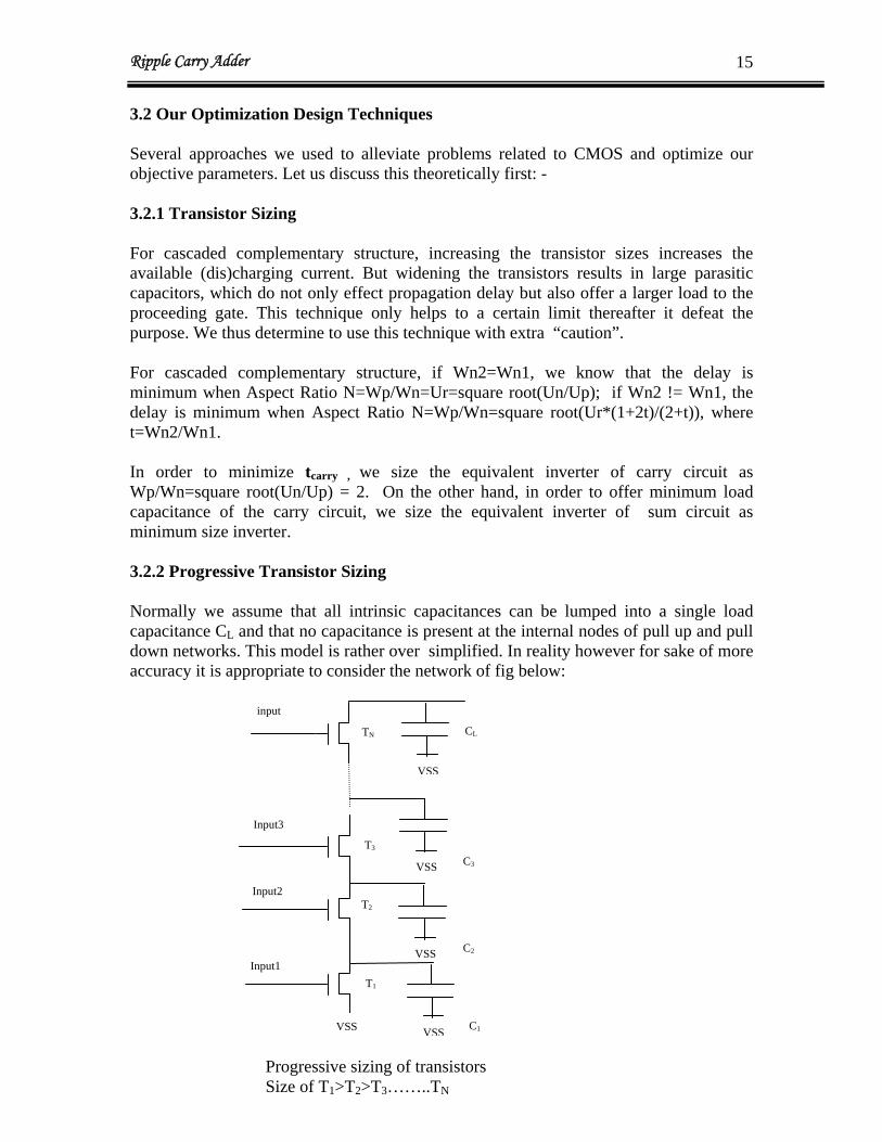
3.2 Our Optimization Design Techniques Several approaches we used to alleviate problems related to CMOS and optimize our objective parameters. Let us discuss this theoretically first: - 3.2.1 Transistor Sizing For cascaded complementary structure, increasing the transistor sizes increases the available (dis)charging current. But widening the transistors results in large parasitic capacitors, which do not only effect propagation delay but also offer a larger load to the proceeding gate. This technique only helps to a certain limit thereafter it defeat the purpose. We thus determine to use this technique with extra “caution”. For cascaded complementary structure, if Wn2=Wn1, we know that the delay is minimum when Aspect Ratio N=Wp/Wn=Ur=square root(Un/Up); if Wn2 != Wn1, the delay is minimum when Aspect Ratio N=Wp/Wn=square root(Ur*(1+2t)/(2+t)), where t=Wn2/Wn1. In order to minimize tcarry , we size the equivalent inverter of carry circuit as Wp/Wn=square root(Un/Up) = 2. On the other hand, in order to offer minimum load capacitance of the carry circuit, we size the equivalent inverter of sum circuit as minimum size inverter. 3.2.2 Progressive Transistor Sizing Normally we assume that all intrinsic capacitances can be lumped into a single load capacitance CL and that no capacitance is present at the internal nodes of pull up and pull down networks. This model is rather over simplified. In reality however for sake of more accuracy it is appropriate to consider the network of fig below:
VSS
input
TN
VSS
VSS
VSSVSS
Input3
Input1
Input2
T3
T1
T2
CL
C2
C3
C1
Progressive sizing of transistors Size of T1>T2>T3……..TN
Ripple Carry Adder 16
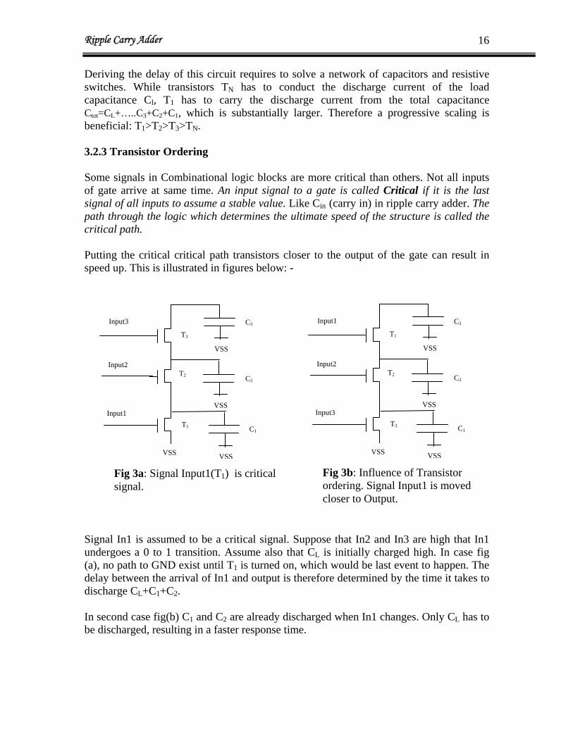
Deriving the delay of this circuit requires to solve a network of capacitors and resistive switches. While transistors TN has to conduct the discharge current of the load capacitance C , Tl 1 has to carry the discharge current from the total capacitance Ctot=C +…..C +C +CL 3 2 1, which is substantially larger. Therefore a progressive scaling is beneficial: T >T1 2>T >T3 N. 3.2.3 Transistor Ordering Some signals in Combinational logic blocks are more critical than others. Not all inputs of gate arrive at same time. An input signal to a gate is called Critical if it is the last signal of all inputs to assume a stable value. Like Cin (carry in) in ripple carry adder. The path through the logic which determines the ultimate speed of the structure is called the critical path. Putting the critical critical path transistors closer to the output of the gate can result in speed up. This is illustrated in figures below: -
VSS
VSS
VSS VSS
Input1
Input3
Input2
T1
T3
T2 C2
C3
C1
Fig 3b: Influence of Transistor ordering. Signal Input1 is moved closer to Output.
VSS
VSS
VSSVSS
Input3
Input1
Input2
T3
T1
T2 C2
C3
C1
Fig 3a: Signal Input1(T1) is critical signal.
Signal In1 is assumed to be a critical signal. Suppose that In2 and In3 are high that In1 undergoes a 0 to 1 transition. Assume also that CL is initially charged high. In case fig (a), no path to GND exist until T1 is turned on, which would be last event to happen. The delay between the arrival of In1 and output is therefore determined by the time it takes to discharge CL+C +C . 1 2 In second case fig(b) C1 and C are already discharged when In1 changes. Only C2 L has to be discharged, resulting in a faster response time.
Ripple Carry Adder 17
3.3 Optimization of delay (tadder) and Simulation We have so far: - • Discussed our optimization theory to meet our desired objective to minimize delay of
ripple carry adder. • Studied above different parameters that influence the propagation of carry. Before we will apply our optimization techniques to size our circuit and simulate the performance, we prefer to discuss minimum size of transistor and test vector. In this section and the following section we would like to provide our simulation results. We have considered Short Channel Model, throughout whole analysis and used SPICE level-13, for our simulations. 3.3.1 Minimum Size of transistor The goal of optimization is delay, meanwhile, we like to use minimum size transistor to reduce area and power as long as this does not slow down the carry generation. In order to have minimum Wn and Wp, we made a model of an equivalent inverter for different Wn and Wp. We translate size of this equivalent inverter to our static CMOS adder and see is tr and tf under 500psec?
• Wn=Wp=0.5μ We have started our analysis considering minimum sizing. When we take Wn=Wp=Ln=Lp=0.5μ. SPICE simulation shows tr and tf are much higher than 500psec violating the rise and fall time constraint given to us. Thus, we have no choice except to discard this size.
• Wn=Wp=0.75μ
In a second attempt we increased width a little bit as Wn=Wp=0.75μ. Yet simulation shows tr = 1nsec not meeting the criteria of 0.5n sec.
• Wn=Wp=1μ
Simulation shows for the size of Wn=Wp=1μ. and Ln=Lp=0.5 μ, tr and tf are smaller than 0.5 nsec. Thus, we concluded Wn=Wp=1μ is the minimum size we take into consideration.
Ripple Carry Adder 18
3.3.2 Test Vector The worse case delay happens when a carry generated at the last significant bit position propagates all the way to the most significant bit. Input signals for tr and tf are 500ps. Output is connected to a 20fF capacitance. For test worse case tplh ,we chose
A : 0111 B : 0001 S : 1000 C : 0111 S4 : 0→1
For test worse case tphl ,we chose
A : 1110 → 1111 B : 0001 → 0001 S : 1111 → 0000 C : 1111
S4 : 1→0 The leftmost bit represents the msb in these test vector. 3.3.3 Transistor Sizing Once we decided minimum size transistor and test vector, next thing is to determine the size that will give optimum delay. First, We implemented CMOS static ripple carry adder as Figure 5. We size the equivalent inverter of sum circuit as minimum size inverter. It means that Wp=Wn=1u, Lp=Ln=0.5u. And then, we size the equivalent inverter of carry circuit as follow:
• Minimum size(Wp=Wn=1μ) For equivalent inverter of Wp=Wn=1μ, SPICE simulation shows tphl=2.03 ns & tplh=1.82ns
• Equal rise and fall time(Wp=4Wn)
For Wp=4μ and Wn=1μ, SPICE simulation shows tphl=2.37ns & tplh=2.22ns
• Wp=√μr Wn For Wp=2Wn as μr=4 and Wn=1, SPICE simulation shows tphl=1.79ns & tplh=1.77ns
Ripple Carry Adder 19
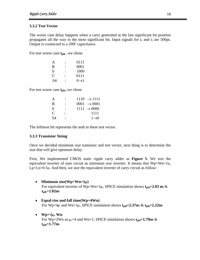
3.3.4 Transistor ordering We implemented CMOS static ripple carry adder as fig 4, and size as Wp=√μr Wn. Spice simulation shows t =2.55ns & tphl plh=2.31ns for Fig4. It is worse than simulated result by using circuit firgue5. The reason is as follow: In group A, group B, group C, group D and group E the transistors connected to Ci should be placed as close as possible to the output of the gate. This is direct application of transistor ordering optimization technique we discussed in section 1 that is transistors on the critical path should be placed as close as possible to the output of the gate. For example, in stage “k” of the adder signal Ak, B are available and stable long before Ck i,k (=Co,k-1) arrives after rippling through previous stages. In this way capacitances of the internal nodes in the transistor chain are precharged or discharged in advance. On arrival of C only the capacitance of node X has to be (dis)charged. Putting Ci,k i,k transistors closer to VDD and GND would require not only (dis)charging of the capacitances of node X but also of internal capacitances.
Fig 6: Transistors whose positions effect the propagation of carry have been gathered into group A, group B, group C, group D and group E.
VSS
S
VDD
VSS
VSS
VSS
VDD
A
A
A
A
A
B B
B
A B
A B Ci
B
Ci
Co
B
CiCi A B
Ci
Co
VSS
A
B
C
x VDD
E
D
Ripple Carry Adder 20
modified circuit diagram is as below: -
VDD
VSSVSS
VSSVSS
VDD
VDD
A
A
A
A
A
A
A B
B
B B
B Ci
B
B
Ci
Co
Ci
Ci
Ci
A B
Co
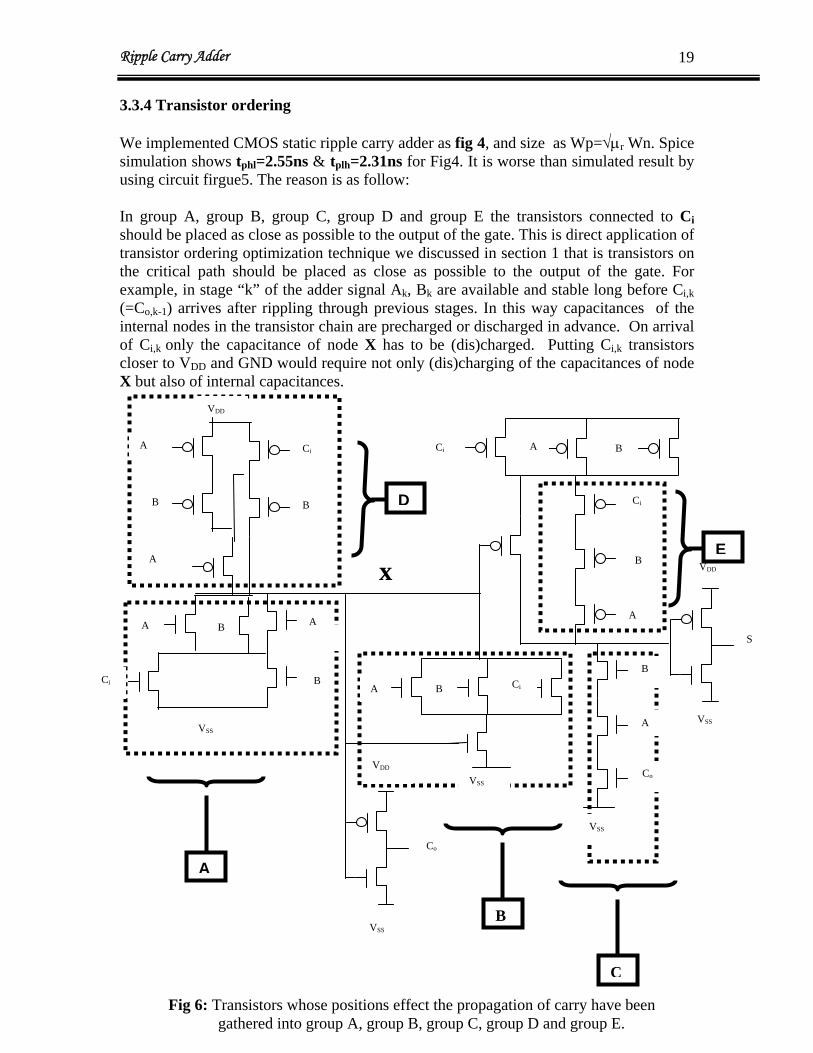
Fig:5 Critical transistors has been placed closer to output
=1.79ns & t =1.77ns for the Fig5.Spice simulation shows tphl plh
Ripple Carry Adder 21
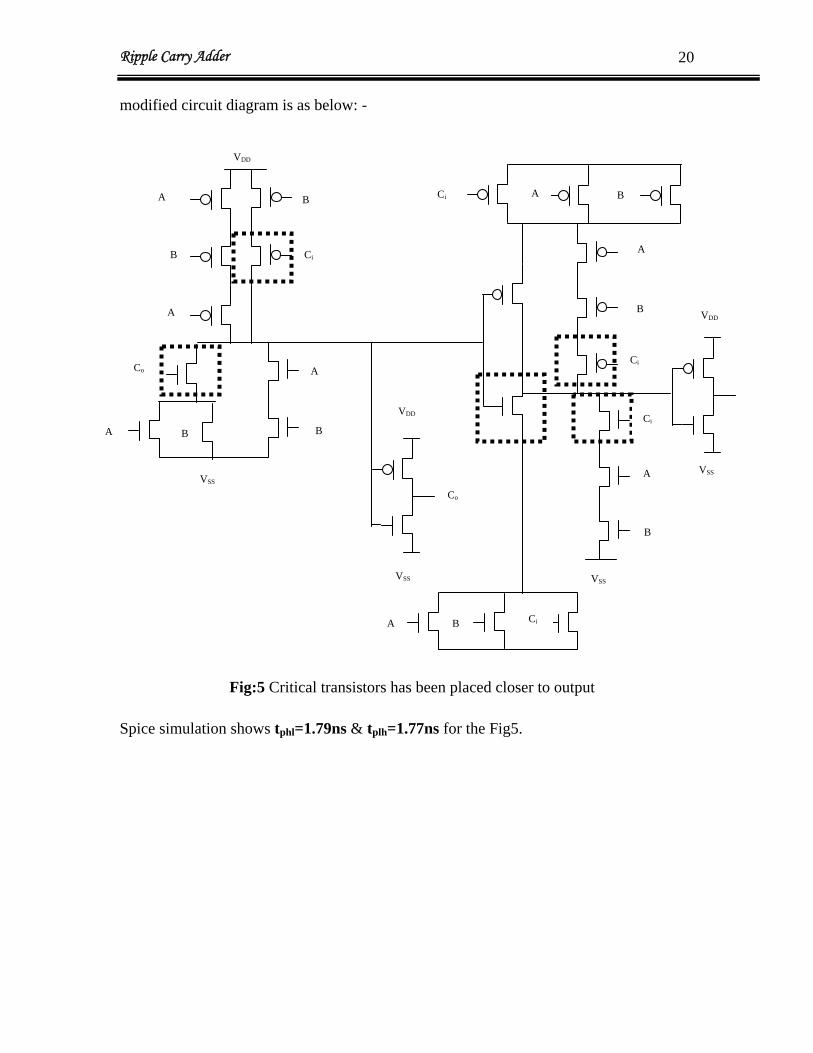
3.3.5 Progressive Transistor Sizing and Extend Size in Critical Path Few transistor sizes of CMOS ripple carry adder in light of above discussion that give optimum delay of tphl=1.79ns and t =1.77ns are shown below: - plh Eventhough, sizes are calculated for optimum delay, but few transistors shown in block A, block B, block C and block D, if size progressively will further optimize the delay. Therefore, we increase the sizes of all transistors in block A from 2μ to 3μ, block B from 2μ to 3μ , block C from 3μ each to 3μ , 4μ and 5μ. Block D 3μ to 4μ. Spice simulation, results depicted in attached diagram, shows t =1.68ns & tphl plh=1.74ns. Attached figure 7 with sizes represents our final schematic.
2μ
Fig:6 Sizes of few critical transistors are shown for optimum delay
3μ
2μ 3μ
VDD
VSSVSS
VSSVSS
VDD
VDD
A
A
A
A
A B
B
B B
A B Ci
B
B
Ci
Co
Ci
Ci
Ci
A B
Co
A
C
B
D
Ripple Carry Adder 22
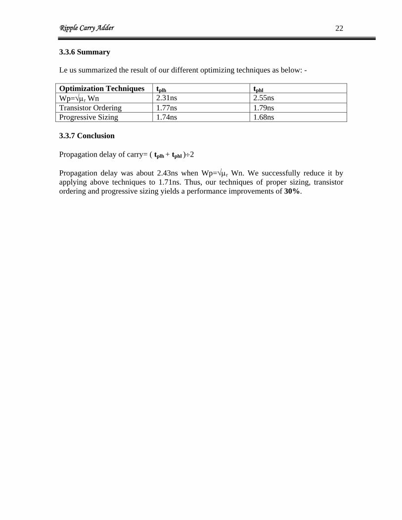
3.3.6 Summary Le us summarized the result of our different optimizing techniques as below: - Optimization Techniques tplh tphl
Wp=√μr Wn 2.31ns 2.55ns Transistor Ordering 1.77ns 1.79ns Progressive Sizing 1.74ns 1.68ns 3.3.7 Conclusion Propagation delay of carry= ( tplh + tphl )÷2 Propagation delay was about 2.43ns when Wp=√μr Wn. We successfully reduce it by applying above techniques to 1.71ns. Thus, our techniques of proper sizing, transistor ordering and progressive sizing yields a performance improvements of 30%.
Ripple Carry Adder 23
Section 4
LAYOUT AND SIMULATION
Ripple Carry Adder 24
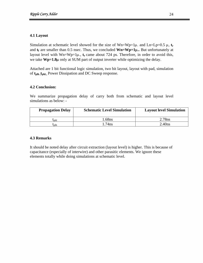
4.1 Layout Simulation at schematic level showed for the size of Wn=Wp=1μ. and Ln=Lp=0.5 μ, tr and tf are smaller than 0.5 nsec. Thus, we concluded Wn=Wp=1μ.. But unfortunately at layout level with Wn=Wp=1μ., tr came about 724 ps. Therefore, in order to avoid this, we take Wp=1.8μ only at SUM part of output inverter while optimizing the delay. Attached are 1 bit functional logic simulation, two bit layout, layout with pad, simulation of tplh ,tphl., Power Dissipation and DC Sweep response. 4.2 Conclusion: We summarize propagation delay of carry both from schematic and layout level simulations as below: -
Propagation Delay Schematic Level Simulation
Layout level Simulation
tphl 1.68ns 2.78ns tplh 1.74ns 2.40ns
4.3 Remarks It should be noted delay after circuit extraction (layout level) is higher. This is because of capacitance (especially of interwire) and other parasitic elements. We ignore these elements totally while doing simulations at schematic level.

Ripple Carry Adder 25
Section 5
OUR ACHIEVEMENTS
Ripple Carry Adder 26
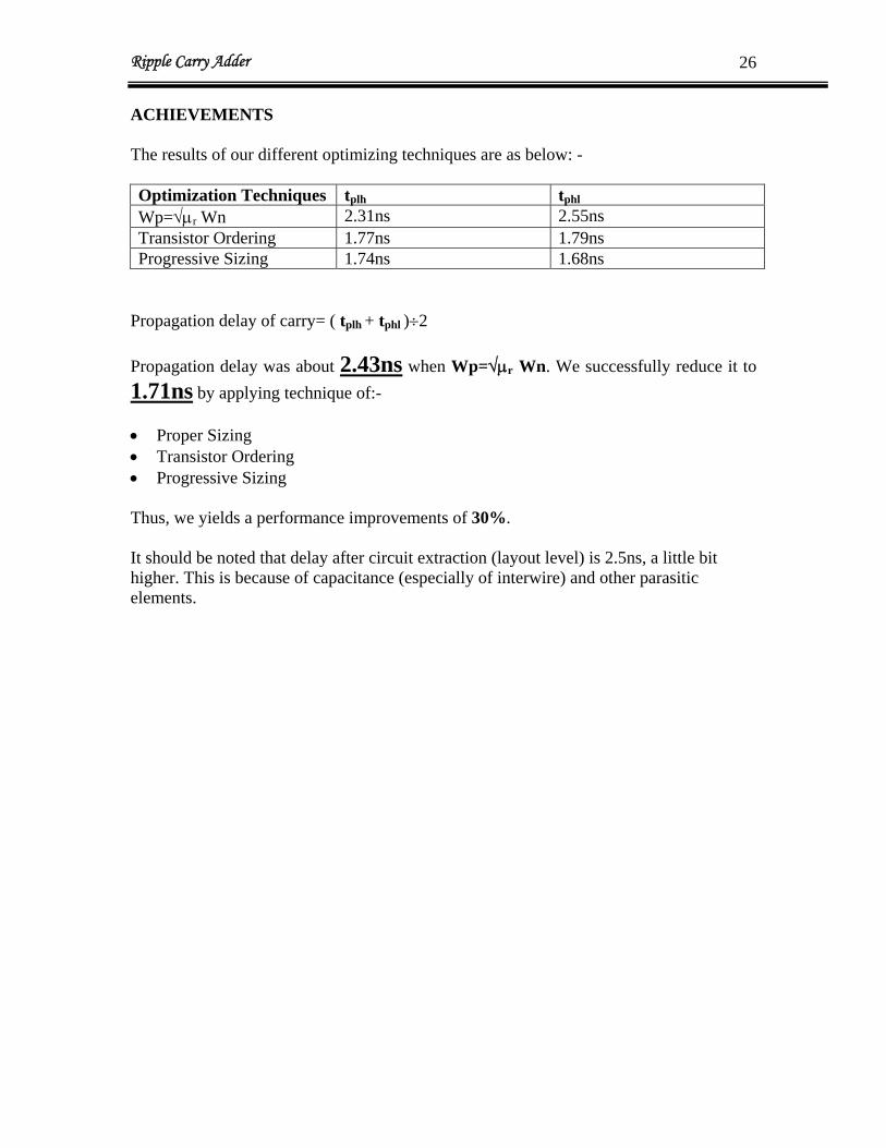
ACHIEVEMENTS The results of our different optimizing techniques are as below: - Optimization Techniques tplh tphl
Wp=√μr Wn 2.31ns 2.55ns Transistor Ordering 1.77ns 1.79ns Progressive Sizing 1.74ns 1.68ns
Propagation delay of carry= ( tplh + tphl )÷2 Propagation delay was about 2.43ns when Wp=√μr Wn. We successfully reduce it to 1.71ns by applying technique of:- • Proper Sizing • Transistor Ordering • Progressive Sizing Thus, we yields a performance improvements of 30%. It should be noted that delay after circuit extraction (layout level) is 2.5ns, a little bit higher. This is because of capacitance (especially of interwire) and other parasitic elements.
Ripple Carry Adder 27
Section 6
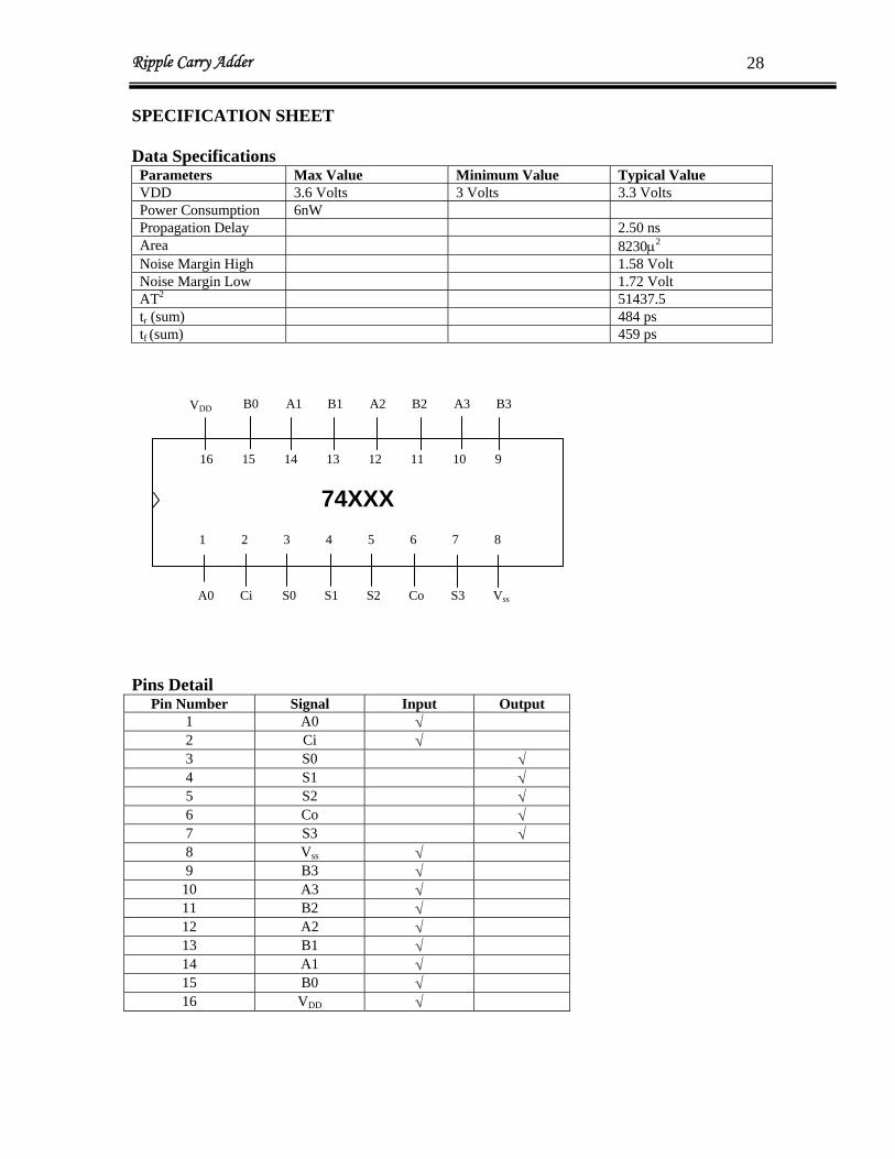
SPECIFICATION SHEET
Ripple Carry Adder 28
SPECIFICATION SHEET Data Specifications
Parameters Max Value Minimum Value Typical Value VDD 3.6 Volts 3 Volts 3.3 Volts Power Consumption 6nW Propagation Delay 2.50 ns Area 8230μ2
Noise Margin High 1.58 Volt Noise Margin Low 1.72 Volt AT2 51437.5 t (sum) 484 ps rtf (sum) 459 ps
74XXX
2 3 4 5 6 1 8 7
15 14 13 12 11 16 9 10
Ci S0 S1 S2 Co A0 VssS3
B0 A1 B1 A2 B2 VDD B3 A3
Pins Detail
Pin Number Signal Input Output 1 A0 √ 2 Ci √ 3 S0 √ 4 S1 √ 5 S2 √ 6 Co √ 7 S3 √ 8 V √ ss
9 B3 √ 10 A3 √ 11 B2 √ 12 A2 √ 13 B1 √ 14 A1 √ 15 B0 √ 16 V √ DD
Ripple Carry Adder 29
Section 7
DESIGN IMPROVEMENT SUGGESTIONS

Ripple Carry Adder 30
Improved Adder Design The speed of our circuit can be improved further by using some of the adder properties. First of all, the number of inverting stages in carry path can be reduced by exploiting the inverting property that is: “Inverting of all inputs to a full adder results in inverted values for all outputs”. This rule will allow us to eliminate an inverting gate in carry chain. This full adder will require only 24 transistors. The disadvantage is that this design would have needed different cells for the even and odd slices of adder chain. This would have complicated the layout design. - Since our focus this time was to keep the things simple and make them work first, we avoided this design in our first attempt. But we commit to implement above mentioned improvements in our next attempt in some other courses.
Ripple Carry Adder 31
Section 8
REFERENCES
Ripple Carry Adder 32
REFERENCES During this entire project, we used the references below: - Digital Design By Morris Mano Digital Integrated Circuit-A Design Perspective By Jan. M.Rabaey Principles of CMOS VLSI design-A System Perspective By Neil H. Weste And of course Dr. Khalili, our advisor, is very helpful throughout this project. We enjoyed Dr. Khalili’s experience advice and guidance to complete this project.