Embed Size (px)
Citation preview
Progress In Electromagnetics Research B, Vol. 59, 151–166, 2014
A Comparative Study of Material Leucaena Leucocephala StemWood Plastic Composite (WPC) Substrate with FR4 Substrate
throughout Single Patch Antenna Design
Ahmad A. Azlan1, *, Muhammad K. A. Badrun1, Mohd T. Ali2,Zaiki Awang2, Zakiah M. Saad1, and Aziati H. Awang2
Abstract—The fabrication of single square patch antenna for proposed Leucaena Leucocephala (“PetaiBelalang”) Wood Plastic Composite (WPC) substrate board (PB Substrate board) and FR4 substrateboard is presented in this paper. The experiment objective is to measure the performance of anantenna fabricated on the FR4 and PB substrate (proposed substrate) by comparing the performancein terms of material’s dielectric constant and electron mobility and antennas’ loss tangent, returnloss (S11), radiation pattern and practical antenna transmitting performance. The new substratecompositions of Leucaena Leucocephala stem and polypropylene (PP) are 30% and 70% consecutively.The result for 150µm (sample B) indicates stability on most dielectric constant (εr = 3.02), losstangent (tan δ = 0.029) and electron mobility (5.31 × 103 cm2/Vs), with the consistency of antennaresult, between simulation and measurement. All results obtained will be analyzed and displayed in theform of data and graphs.
1. INTRODUCTION
“Green Technology Product” evolves from various kinds of techniques, methodologies and enhancementof various materials conserve the natural environment and resources, which minimizes and reduces thenegative impact of human activities. The implementation of green technology especially on developingnew material product will be an option to the industry and also the government in driving new economicgrowth by contributing to fiscal consolidation, enhancing productivity through greater efficiency in theuse of natural and reusable resources [1–4]. Green technology product development, sustainability,cradle to cradle design and its viability are the major issues of this technology, whereby the productdevelopment can last indefinitely into the future without damaging or depleting natural resources,hence it can be fully reclaimed or reused [5–8]. The research of green technology product not only isrelated to energy saving, renewable energy and building material fabrication, but also can be expandedto the fabrication of Printed Circuit Board (PCB) which is now widely used as the substrate ofplanar antenna [9–12]. Existing substrate product, for example substrate from the Rogers CorporationCompany and Taconic Company, is widely used as a substrate to fabricate high-end planar antennasystem [13–16]. Existing substrate products, such as substrates from the Rogers Corporation Companyand Taconic Company, are widely used to fabricate high end planar antenna system [13–16]. Thefabricated antennas on both of these commercially available substrates seem to be very stable andhighly efficient. However, the drawback is that it is very expensive if the antenna design is in massproduction.
Received 2 February 2014, Accepted 4 April 2014, Scheduled 9 April 2014* Corresponding author: Ahmad Aziz Azlan ([email protected]).1 Center of Medical Electronic Technology (CMET), Sultan Salahuddin Abdul Aziz Shah Polytechnic, Persiaran Usahawan Seksyenu1, Shah Alam Selangor, Malaysia. 2Antenna Research Group (ARG), Microwave Technology Center (MTC), Faculty of ElectricalEngineering (FKE), UiTM, Shah Alam, Selangor 40450, Malaysia.
152 Azlan et al.
In order to get cheaper substrates while not compromising the antenna performance, fiber glassmaterial substrate (FR4) is the alternative solution, and relatively excellent results are obtained in spiteof using cheaper FR4 material substrate [17, 18]. The goal for this research is to find other potentialmaterials that can be used as antenna substrate with additional value, following the green technologyproduct criteria and with better antenna performance than FR4 substrate material. The proposedsubstrate board used undergoes the process of Wood Plastic Composite (WPC) technique with hotand cold press machine fabrication method. The elaboration of the method will be discussed in thesubstrate fabrication method setup section. WPC can be obtained from a mixture of thermoplasticpolymer and saw dust wood. The thermoplastic polymer can be Acrylic (methyl methacrylate),Polyethylene (PE), Polystyrene (PS), Polyvinyl chloride (PVC), polytetrafluoroethylene (PTFE) orTeflon and Polypropylene (PP). In this research paper, the fabrications are focused on PP since themelting point and resistance to temperature is high compared to other thermoplastic polymers. Themelting point of PP is about 180C.
The saw dust wood filler for this research paper will be from leucaena leucocephala stem. InMalaysia, leucaena leucocephala tree is known as “Petai Belalang”, and the popular tropical treeespecially on the leaf is traditionally known to cure high blood pressure. These wild trees were originallyfound in Central America and Mexico; they spread all around the world including Asia and Malaysia.The tree can be harvested after 1 to 2 years of growth, and the application of the tree is still neglectedand under-utilized [19]. WPC has currently become an important research that has gained popularityover the last decade especially with its properties and advantages. Among them are the high durability,low maintenance, acceptable relative strength and stiffness, low price relatives to other competingmaterials, and the fact that it is a natural resource or eco green technology. The high water contentaffects the whole board performance not only on mechanical properties, but also on its electromagneticproperties [20], compared to the used whole wood contents. Other advantages of the usage of WPC aretheir resistance towards biological deterioration especially for outdoor applications.
In order to verify the usage of the proposed substrate in the surrounding of electromagnetic andantenna substrate, the measurements of dielectric constant (εr) and loss tangent (tan δ) seem verysignificant. Dielectric properties of a material define the physical-chemical properties related to thestorage and loss of energy contained in a material or substance. The knowledge of a material’s dielectricproperty is necessary in determining its suitability for a specific application. FR4 material is widely usedas a substrate on most of the antenna designs, and the dielectric constant of the material is between 4.3to 4.9 [21, 22]. The dielectric constant and tangent loss value will be used to design single patch antennain order to obtain the performance of each design. The overall antenna design parameters are given inTable 1, whereby the proposed leucaena leucocephala stem substrate board is noted as PB substrateboard. As indicate in Table 1, the thickness of the copper sheet used was 0.35 mm (350µm). The coppersheet was then cut by using laser cutter machine to square shape and attached to the material by usingthe epoxy (VT-146 rapid 3 Ton 4 minute non-conductive).
Table 1. Basic antenna design parameter.
Substrate PB Board FR4 BoardSubstrate Thickness (mm) 1.6 1.6
Design Center Frequency (GHz) 2.45 2.45Copper thickness (mm) 0.35 0.35
Note: PB Board (Petai Belalang Board).
2. SAMPLE PB SUBSTRATE FABRICATION SETUP
Five PB material samples composed of 70% PP and 30% wood filler were prepared and fabricatedearlier before the measurement began. For the purpose of testing, four different samples were alreadyfabricated with 30% of wood filler mix with 70% of PP. The moisture content of the filler was controlledand maintained at < 16% according to American Society for Testing and Materials (ASTM) D5456standard. The thickness and dimension of the sample were fixed to 1.6 mm and 150mm× 150mm. The
Progress In Electromagnetics Research B, Vol. 59, 2014 153
Table 2. Sample parameter of material mixing.
Sample % Filler % Polypropylene (PP) Particle size Substrate thicknessA1 0 100 0 1.6mmA 30 70 100µm 1.6mmB 30 70 150µm 1.6mmC 30 70 250µm 1.6mmD 30 70 500µm 1.6mm
Note:Sample A1: Pure PP substrate board with 0% of Sawdust Wood;
Sample A: PB substrate board 100 µm sawdust wood particle;Sample B: PB substrate board 150 µm sawdust wood particle;Sample C: PB substrate board 200 µm sawdust wood particle;Sample D: PB substrate board 500 µm sawdust wood particle.
parameter that varies between these four samples was only the particle size of the sample. Table 2below shows the five sampled parameters.
The proposed PB board was fabricated with the ratio of 70 percent of PP and 30 percent of LeucaenaLeucocephala sawdust filler. The main filler is taken from the tree trunk with 2 years of growth age.The filler is cut into different particle sizes to vary the wood behavior. The different particle sizeswere also shown in Table 2. Figure 1 below shows the raw material of wood plastic composite (WPC)fabrication.
(a) (b)
Figure 1. Wood plastic composite raw material: (a) PP crystalline, (b) Leucaena Leucocephala stemsSawdust filler.
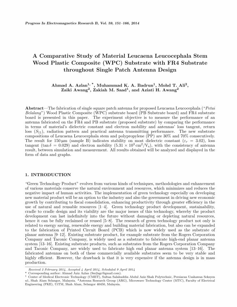
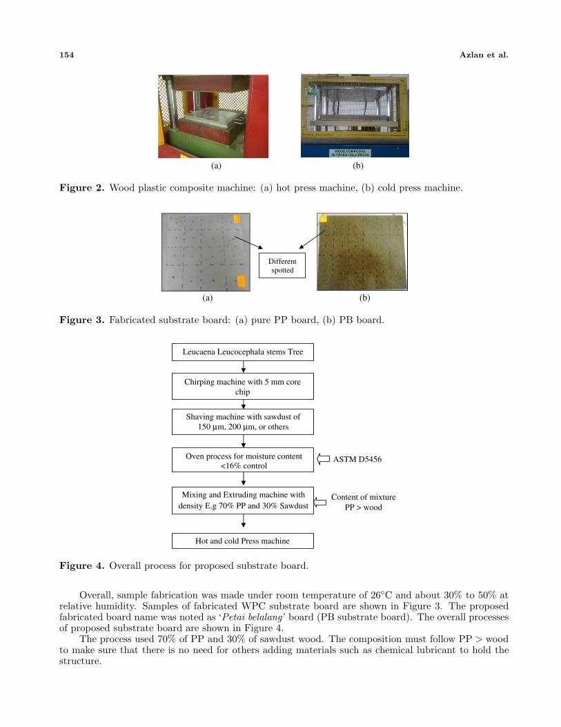
Preparation of the sample of WPC is in accordance to the ASTM D1238 standard, and the meltingpoint for the fabrication is set to 180C with melting index of 12 g/10 min [23]. The melting processoccupied two main machines that were hot press machine and cold press machine. The hot and cold pressmachines are shown in Figure 2. Most of the fabrication method of WPC can be obtained in [25, 26].
Transferring the WPC sample from hot pressing machine to cold pressing machine has to be doneimmediately in order to preserve the molecule of PP structure and hence the rigidity of the sample.The temperature of the cold press machine is set to 20C with duration of 120 second [26]. The overallsetting of hot and cold press machines can be viewed in Table 3.
Table 3. Hot and cold press machine setting.
Hot Press Setting Cold Press SettingTemperature: 180C Temperature: 20CPressure: 1000 psi Pressure: 500 psi
Duration: 330 Seconds Duration: 120 Seconds
154 Azlan et al.
(a) (b)
Figure 2. Wood plastic composite machine: (a) hot press machine, (b) cold press machine.
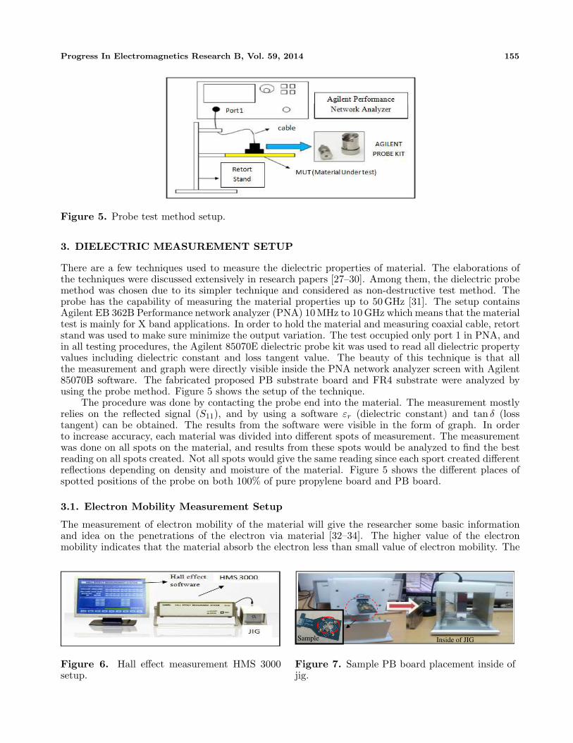
Different
spotted
(a) (b)
Figure 3. Fabricated substrate board: (a) pure PP board, (b) PB board.
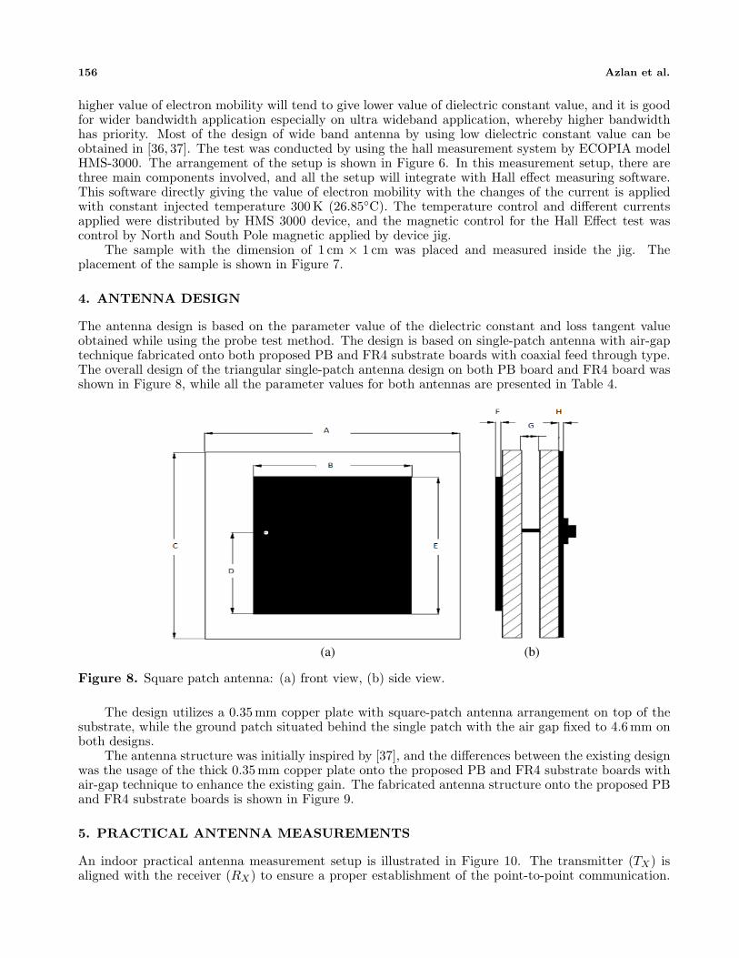
Leucaena Leucocephala stems Tree
Chirping machine with 5 mm core
chip
Shaving machine with sawdust of
150 µm, 200 µm, or others
Oven process for moisture content<16% control
ASTM D5456
Mixing and Extruding machine with
density E.g 70% PP and 30% SawdustContent of mixture
PP > wood
Hot and cold Press machine
Figure 4. Overall process for proposed substrate board.
Overall, sample fabrication was made under room temperature of 26C and about 30% to 50% atrelative humidity. Samples of fabricated WPC substrate board are shown in Figure 3. The proposedfabricated board name was noted as ‘Petai belalang ’ board (PB substrate board). The overall processesof proposed substrate board are shown in Figure 4.
The process used 70% of PP and 30% of sawdust wood. The composition must follow PP > woodto make sure that there is no need for others adding materials such as chemical lubricant to hold thestructure.
Progress In Electromagnetics Research B, Vol. 59, 2014 155
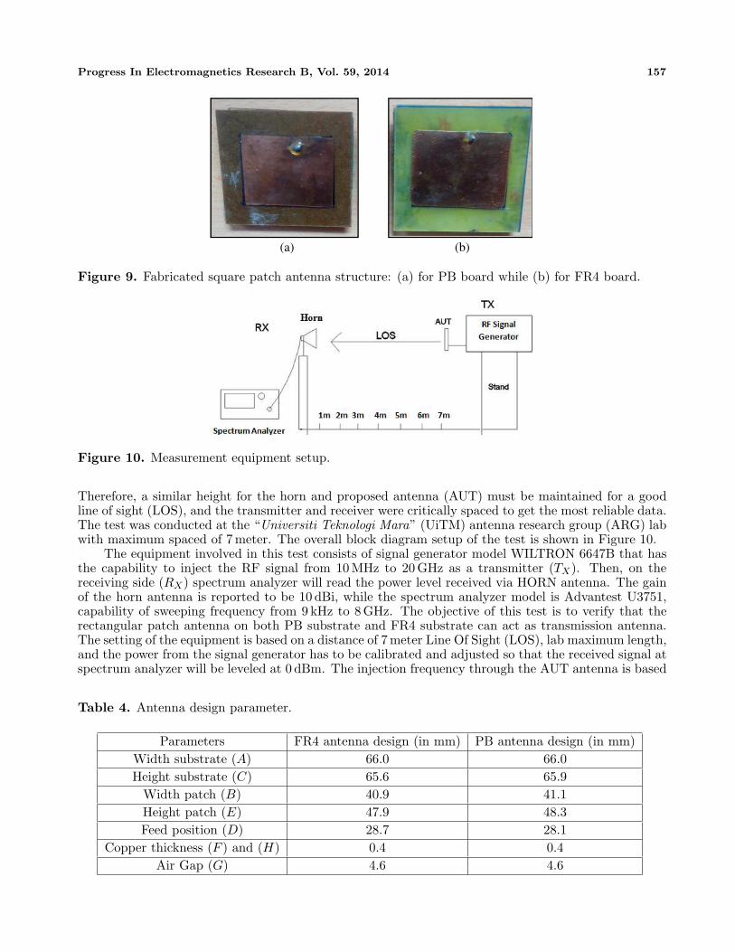
Figure 5. Probe test method setup.
3. DIELECTRIC MEASUREMENT SETUP
There are a few techniques used to measure the dielectric properties of material. The elaborations ofthe techniques were discussed extensively in research papers [27–30]. Among them, the dielectric probemethod was chosen due to its simpler technique and considered as non-destructive test method. Theprobe has the capability of measuring the material properties up to 50 GHz [31]. The setup containsAgilent EB 362B Performance network analyzer (PNA) 10 MHz to 10 GHz which means that the materialtest is mainly for X band applications. In order to hold the material and measuring coaxial cable, retortstand was used to make sure minimize the output variation. The test occupied only port 1 in PNA, andin all testing procedures, the Agilent 85070E dielectric probe kit was used to read all dielectric propertyvalues including dielectric constant and loss tangent value. The beauty of this technique is that allthe measurement and graph were directly visible inside the PNA network analyzer screen with Agilent85070B software. The fabricated proposed PB substrate board and FR4 substrate were analyzed byusing the probe method. Figure 5 shows the setup of the technique.
The procedure was done by contacting the probe end into the material. The measurement mostlyrelies on the reflected signal (S11), and by using a software εr (dielectric constant) and tan δ (losstangent) can be obtained. The results from the software were visible in the form of graph. In orderto increase accuracy, each material was divided into different spots of measurement. The measurementwas done on all spots on the material, and results from these spots would be analyzed to find the bestreading on all spots created. Not all spots would give the same reading since each sport created differentreflections depending on density and moisture of the material. Figure 5 shows the different places ofspotted positions of the probe on both 100% of pure propylene board and PB board.
3.1. Electron Mobility Measurement Setup
The measurement of electron mobility of the material will give the researcher some basic informationand idea on the penetrations of the electron via material [32–34]. The higher value of the electronmobility indicates that the material absorb the electron less than small value of electron mobility. The
Figure 6. Hall effect measurement HMS 3000setup.
Sample Inside of JIG
Figure 7. Sample PB board placement inside ofjig.
156 Azlan et al.
higher value of electron mobility will tend to give lower value of dielectric constant value, and it is goodfor wider bandwidth application especially on ultra wideband application, whereby higher bandwidthhas priority. Most of the design of wide band antenna by using low dielectric constant value can beobtained in [36, 37]. The test was conducted by using the hall measurement system by ECOPIA modelHMS-3000. The arrangement of the setup is shown in Figure 6. In this measurement setup, there arethree main components involved, and all the setup will integrate with Hall effect measuring software.This software directly giving the value of electron mobility with the changes of the current is appliedwith constant injected temperature 300K (26.85C). The temperature control and different currentsapplied were distributed by HMS 3000 device, and the magnetic control for the Hall Effect test wascontrol by North and South Pole magnetic applied by device jig.
The sample with the dimension of 1 cm × 1 cm was placed and measured inside the jig. Theplacement of the sample is shown in Figure 7.
4. ANTENNA DESIGN
The antenna design is based on the parameter value of the dielectric constant and loss tangent valueobtained while using the probe test method. The design is based on single-patch antenna with air-gaptechnique fabricated onto both proposed PB and FR4 substrate boards with coaxial feed through type.The overall design of the triangular single-patch antenna design on both PB board and FR4 board wasshown in Figure 8, while all the parameter values for both antennas are presented in Table 4.
(a) (b)
Figure 8. Square patch antenna: (a) front view, (b) side view.
The design utilizes a 0.35 mm copper plate with square-patch antenna arrangement on top of thesubstrate, while the ground patch situated behind the single patch with the air gap fixed to 4.6 mm onboth designs.
The antenna structure was initially inspired by [37], and the differences between the existing designwas the usage of the thick 0.35 mm copper plate onto the proposed PB and FR4 substrate boards withair-gap technique to enhance the existing gain. The fabricated antenna structure onto the proposed PBand FR4 substrate boards is shown in Figure 9.
5. PRACTICAL ANTENNA MEASUREMENTS
An indoor practical antenna measurement setup is illustrated in Figure 10. The transmitter (TX) isaligned with the receiver (RX) to ensure a proper establishment of the point-to-point communication.
Progress In Electromagnetics Research B, Vol. 59, 2014 157
(a) (b)
Figure 9. Fabricated square patch antenna structure: (a) for PB board while (b) for FR4 board.
Figure 10. Measurement equipment setup.
Therefore, a similar height for the horn and proposed antenna (AUT) must be maintained for a goodline of sight (LOS), and the transmitter and receiver were critically spaced to get the most reliable data.The test was conducted at the “Universiti Teknologi Mara” (UiTM) antenna research group (ARG) labwith maximum spaced of 7meter. The overall block diagram setup of the test is shown in Figure 10.
The equipment involved in this test consists of signal generator model WILTRON 6647B that hasthe capability to inject the RF signal from 10 MHz to 20 GHz as a transmitter (TX). Then, on thereceiving side (RX) spectrum analyzer will read the power level received via HORN antenna. The gainof the horn antenna is reported to be 10 dBi, while the spectrum analyzer model is Advantest U3751,capability of sweeping frequency from 9 kHz to 8GHz. The objective of this test is to verify that therectangular patch antenna on both PB substrate and FR4 substrate can act as transmission antenna.The setting of the equipment is based on a distance of 7meter Line Of Sight (LOS), lab maximum length,and the power from the signal generator has to be calibrated and adjusted so that the received signal atspectrum analyzer will be leveled at 0 dBm. The injection frequency through the AUT antenna is based
Table 4. Antenna design parameter.
Parameters FR4 antenna design (in mm) PB antenna design (in mm)Width substrate (A) 66.0 66.0Height substrate (C) 65.6 65.9
Width patch (B) 40.9 41.1Height patch (E) 47.9 48.3Feed position (D) 28.7 28.1
Copper thickness (F ) and (H) 0.4 0.4Air Gap (G) 4.6 4.6
158 Azlan et al.
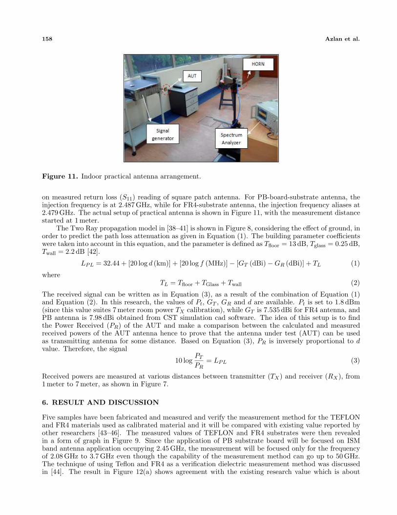
Figure 11. Indoor practical antenna arrangement.
on measured return loss (S11) reading of square patch antenna. For PB-board-substrate antenna, theinjection frequency is at 2.487GHz, while for FR4-substrate antenna, the injection frequency aliases at2.479GHz. The actual setup of practical antenna is shown in Figure 11, with the measurement distancestarted at 1meter.
The Two Ray propagation model in [38–41] is shown in Figure 8, considering the effect of ground, inorder to predict the path loss attenuation as given in Equation (1). The building parameter coefficientswere taken into account in this equation, and the parameter is defined as Tfloor = 13 dB, Tglass = 0.25 dB,Twall = 2.2 dB [42].
LPL = 32.44 + [20 log d (km)] + [20 log f (MHz)]− [GT (dBi)−GR (dBi)] + TL (1)
whereTL = Tfloor + TGlass + Twall (2)
The received signal can be written as in Equation (3), as a result of the combination of Equation (1)and Equation (2). In this research, the values of Pt, GT , GR and d are available. Pt is set to 1.8 dBm(since this value suites 7meter room power TX calibration), while GT is 7.535 dBi for FR4 antenna, andPB antenna is 7.98 dBi obtained from CST simulation cad software. The idea of this setup is to findthe Power Received (PR) of the AUT and make a comparison between the calculated and measuredreceived powers of the AUT antenna hence to prove that the antenna under test (AUT) can be usedas transmitting antenna for some distance. Based on Equation (3), PR is inversely proportional to dvalue. Therefore, the signal
10 logPT
PR= LPL (3)
Received powers are measured at various distances between transmitter (TX) and receiver (RX), from1meter to 7 meter, as shown in Figure 7.
6. RESULT AND DISCUSSION
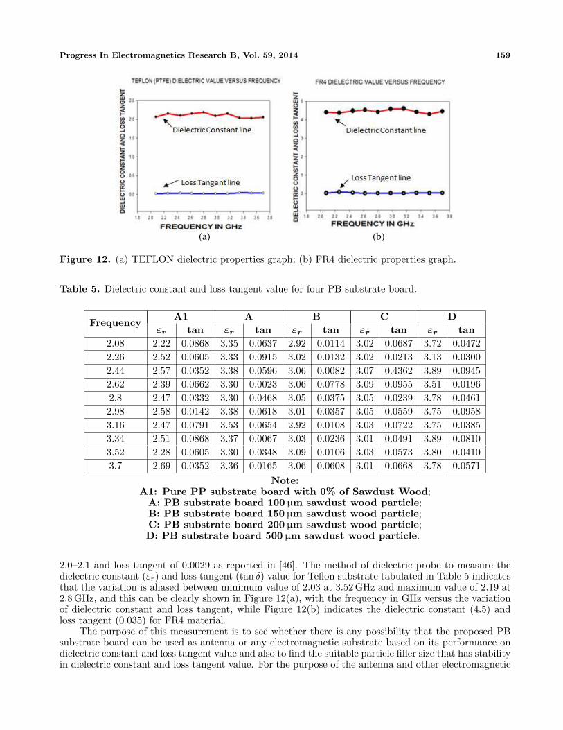
Five samples have been fabricated and measured and verify the measurement method for the TEFLONand FR4 materials used as calibrated material and it will be compared with existing value reported byother researchers [43–46]. The measured values of TEFLON and FR4 substrates were then revealedin a form of graph in Figure 9. Since the application of PB substrate board will be focused on ISMband antenna application occupying 2.45 GHz, the measurement will be focused only for the frequencyof 2.08 GHz to 3.7 GHz even though the capability of the measurement method can go up to 50 GHz.The technique of using Teflon and FR4 as a verification dielectric measurement method was discussedin [44]. The result in Figure 12(a) shows agreement with the existing research value which is about
Progress In Electromagnetics Research B, Vol. 59, 2014 159
(a) (b)
Figure 12. (a) TEFLON dielectric properties graph; (b) FR4 dielectric properties graph.
Table 5. Dielectric constant and loss tangent value for four PB substrate board.
FrequencyA1 A B C D
εr tan εr tan εr tan εr tan εr tan2.08 2.22 0.0868 3.35 0.0637 2.92 0.0114 3.02 0.0687 3.72 0.04722.26 2.52 0.0605 3.33 0.0915 3.02 0.0132 3.02 0.0213 3.13 0.03002.44 2.57 0.0352 3.38 0.0596 3.06 0.0082 3.07 0.4362 3.89 0.09452.62 2.39 0.0662 3.30 0.0023 3.06 0.0778 3.09 0.0955 3.51 0.01962.8 2.47 0.0332 3.30 0.0468 3.05 0.0375 3.05 0.0239 3.78 0.04612.98 2.58 0.0142 3.38 0.0618 3.01 0.0357 3.05 0.0559 3.75 0.09583.16 2.47 0.0791 3.53 0.0654 2.92 0.0108 3.03 0.0722 3.75 0.03853.34 2.51 0.0868 3.37 0.0067 3.03 0.0236 3.01 0.0491 3.89 0.08103.52 2.28 0.0605 3.30 0.0348 3.09 0.0106 3.03 0.0573 3.80 0.04103.7 2.69 0.0352 3.36 0.0165 3.06 0.0608 3.01 0.0668 3.78 0.0571
Note:A1: Pure PP substrate board with 0% of Sawdust Wood;
A: PB substrate board 100 µm sawdust wood particle;B: PB substrate board 150 µm sawdust wood particle;C: PB substrate board 200 µm sawdust wood particle;D: PB substrate board 500 µm sawdust wood particle.
2.0–2.1 and loss tangent of 0.0029 as reported in [46]. The method of dielectric probe to measure thedielectric constant (εr) and loss tangent (tan δ) value for Teflon substrate tabulated in Table 5 indicatesthat the variation is aliased between minimum value of 2.03 at 3.52 GHz and maximum value of 2.19 at2.8GHz, and this can be clearly shown in Figure 12(a), with the frequency in GHz versus the variationof dielectric constant and loss tangent, while Figure 12(b) indicates the dielectric constant (4.5) andloss tangent (0.035) for FR4 material.
The purpose of this measurement is to see whether there is any possibility that the proposed PBsubstrate board can be used as antenna or any electromagnetic substrate based on its performance ondielectric constant and loss tangent value and also to find the suitable particle filler size that has stabilityin dielectric constant and loss tangent value. For the purpose of the antenna and other electromagnetic
160 Azlan et al.
usages, the verification mostly relies on dielectric constant and loss tangent of proposed materials. Theoverall value of dielectric constant and loss tangent value for a variation of filler mixture particle sizeare given in Table 5. Before any claim can be made based on result of which particle mixture is betterin term of stability the variation, a pure PP board has to be tested, and in this research the substrateboard noted as A1 was fabricated. In this fabrication, the substrate boards were based on 100% mixtureof pure PP as shown in Figure 3(a). The results of pure PP board are also given in Table 5.
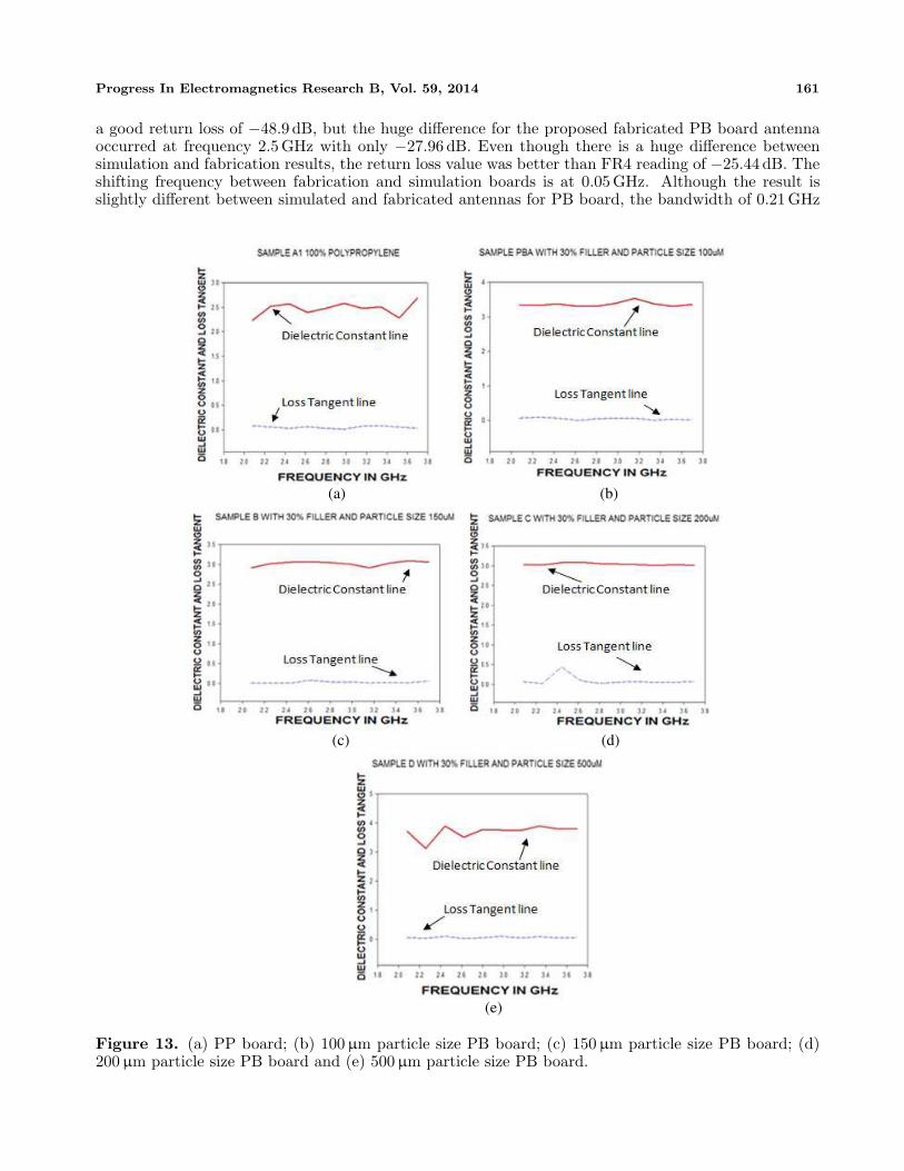
As indicated in Table 5, there is no significant difference between sample A1 and previous PPsubstrate data reported by [45]. The dielectric constant for fabricated PP substrate varies from 2.22 to2.69. The average dielectric constant for sample A (100µm) was 3.4, while those for sample B (150µm)and sample C (200µm) were reported at 3.0 and for sample D (500µm) at 3.7. From Table 5 it is clearlyindicated that there is no significant difference among samples A to D in term of dielectric constantvalue. This result indicates that the dielectric constant value does not depend much on the particlesize. From Table 5 it is clearly indicated that the pure PP substrate (sample A1) rises from average2.2 to 3.0 of dielectric constant value. This situation occurs when the carbon content from the fillerrises [47]. Table 5 shows the average of 0.04 loss tangent reported by sample A, while 0.02 for sampleB, and 0.09 and 0.05 reported for sample C and Sample D. So it can be concluded that the most stabledielectric constant value and loss tangent value on most of the samples is shown by sample B. That iswhy sample B was chosen for antenna fabrication as shown in Figure 9(a). Figures 13(a)–13(e) indicatethe graphs for all the substrates indicated in Table 5.
As indicated in Figures 13(a) to 13(e), the most stable values of dielectric constant and loss tangentvalue are reported by Figure 13(c), with 150µm sawdust particle. Even though Figure 13(d) gives aconstant value for dielectric constant, there is a huge variation on loss tangent reported on frequency2.4GHz. In Figure 13(b), there is a constant value on both dielectric constant and loss tangent, butlow dielectric constant value substrate with 150µm sawdust wood shows better result and fulfills ourobjective to get constant reading on both dielectric constant and loss tangent value while maintaininglow value of dielectric constant value.
Besides measuring the dielectric properties of any proposed material, the overall parameter of anysubstrate can also be gauged by its electron mobility. The result later will show the differences inelectron mobility between FR4 substrate board and PB substrate board with 150µm particle size sincethis proposed PB board shows stability in the dielectric parameter compared to other particle sizes.
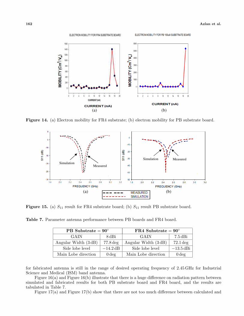
Figure 14(a) and Figure 14(b) indicate the electron mobility for FR4 substrate and proposed PBsubstrate. It is clear to conclude that by referring to Table 6 above, the proposed PB substrate boardshow higher electron mobility with 5.31 × 103 cm2V−1
s , compared to FR4 1.40 × 103 cm2V−1s . The
difference between these two substrates is about 3.91 × 103 cm2V−1s , but dielectric constant does not
show significant difference on the two results. It is also confirmed that higher value of electron mobilitywill lead to low value of dielectric constant, and electron can easily pass through compared to the lowerreading of electron mobility recorded by FR4 compared to PB board.
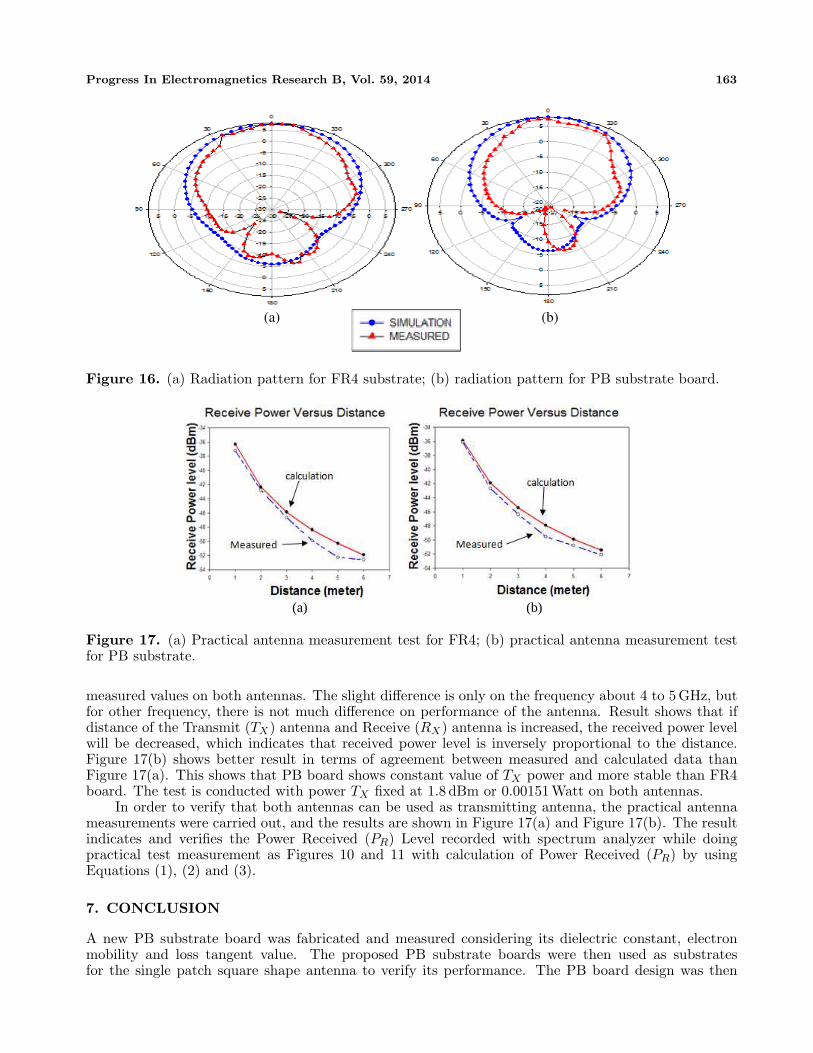
As shown in Figure 15(a), the return loss for simulation FR4 board occurred at 2.45GHz with−25.8 dB, while for the measured value the peak was reported at 2.47GHz with −25.44 dB. This S11
result indicates that the differences between measurement and simulation for FR4 board are frequencyof 0.02 GHz and return loss of −0.36 dB. The result shows that the board design is more stable on S11
reading since there is not much shifting in frequency between simulation and measurement. The targetfrequency of 2.45 GHz is still covered for measured FR4 antenna. The bandwidths reported for practicaland simulated antennas were identical to bandwidth of 0.1809 GHz, which shows good reading on S11
result for FR4 board since the results on fabricated and simulated antennas seem identical. The onlydifference is only the frequency shifting a little bit but still in the range of desired operating frequency.As shown in Figure 15(b), the operating frequency for simulation PB board was set to 2.45GHz with
Table 6. Electron mobility and resistivity of substrate.
Sample Electron Mobility (cm2/Vs) Resistivity (Ω cm)FR4 Board 1.40× 10³ 47.5
PB 150µm board 5.31× 10³ 10.8
Progress In Electromagnetics Research B, Vol. 59, 2014 161
a good return loss of −48.9 dB, but the huge difference for the proposed fabricated PB board antennaoccurred at frequency 2.5 GHz with only −27.96 dB. Even though there is a huge difference betweensimulation and fabrication results, the return loss value was better than FR4 reading of −25.44 dB. Theshifting frequency between fabrication and simulation boards is at 0.05 GHz. Although the result isslightly different between simulated and fabricated antennas for PB board, the bandwidth of 0.21 GHz
(a) (b)
(c) (d)
(e)
Figure 13. (a) PP board; (b) 100µm particle size PB board; (c) 150µm particle size PB board; (d)200µm particle size PB board and (e) 500µm particle size PB board.
162 Azlan et al.
(a) (b)
Figure 14. (a) Electron mobility for FR4 substrate; (b) electron mobility for PB substrate board.
SimulationMeasured
MeasuredSimulation
(a) (b)
Figure 15. (a) S11 result for FR4 substrate board; (b) S11 result PB substrate board.
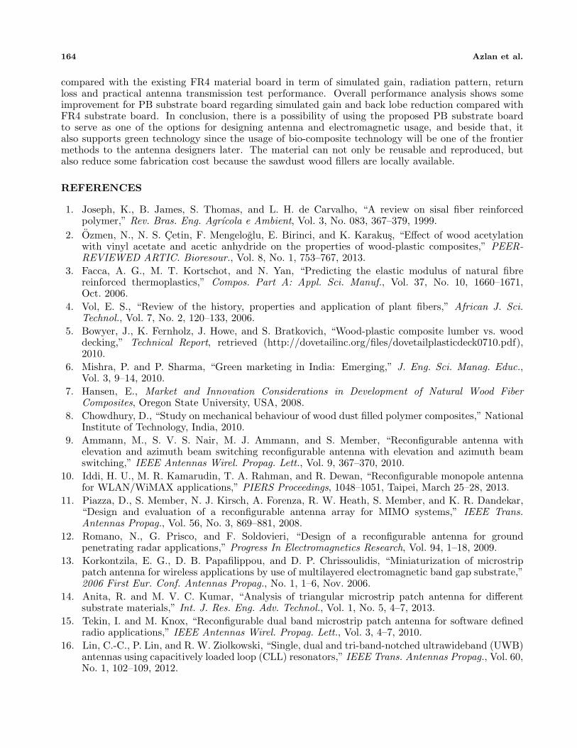
Table 7. Parameter antenna performance between PB boards and FR4 board.
PB Substrate = 90 FR4 Substrate = 90
GAIN 8dBi GAIN 7.5 dBiAngular Width (3 dB) 77.8 deg Angular Width (3 dB) 72.1 deg
Side lobe level −14.2 dB Side lobe level −13.5 dBiMain Lobe direction 0 deg Main Lobe direction 0 deg
for fabricated antenna is still in the range of desired operating frequency of 2.45 GHz for IndustrialScience and Medical (ISM) band antenna.
Figure 16(a) and Figure 16(b) illustrate that there is a huge difference on radiation pattern betweensimulated and fabricated results for both PB substrate board and FR4 board, and the results aretabulated in Table 7.
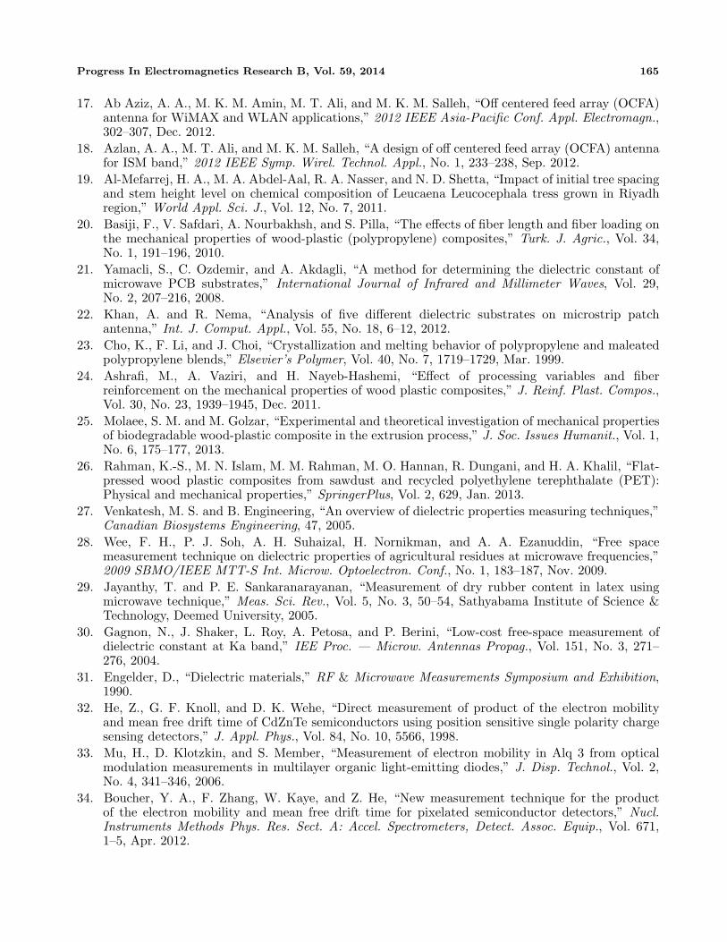
Figure 17(a) and Figure 17(b) show that there are not too much difference between calculated and
Progress In Electromagnetics Research B, Vol. 59, 2014 163
(a) (b)
Figure 16. (a) Radiation pattern for FR4 substrate; (b) radiation pattern for PB substrate board.
(a) (b)
Figure 17. (a) Practical antenna measurement test for FR4; (b) practical antenna measurement testfor PB substrate.
measured values on both antennas. The slight difference is only on the frequency about 4 to 5 GHz, butfor other frequency, there is not much difference on performance of the antenna. Result shows that ifdistance of the Transmit (TX) antenna and Receive (RX) antenna is increased, the received power levelwill be decreased, which indicates that received power level is inversely proportional to the distance.Figure 17(b) shows better result in terms of agreement between measured and calculated data thanFigure 17(a). This shows that PB board shows constant value of TX power and more stable than FR4board. The test is conducted with power TX fixed at 1.8 dBm or 0.00151Watt on both antennas.
In order to verify that both antennas can be used as transmitting antenna, the practical antennameasurements were carried out, and the results are shown in Figure 17(a) and Figure 17(b). The resultindicates and verifies the Power Received (PR) Level recorded with spectrum analyzer while doingpractical test measurement as Figures 10 and 11 with calculation of Power Received (PR) by usingEquations (1), (2) and (3).
7. CONCLUSION
A new PB substrate board was fabricated and measured considering its dielectric constant, electronmobility and loss tangent value. The proposed PB substrate boards were then used as substratesfor the single patch square shape antenna to verify its performance. The PB board design was then
164 Azlan et al.
compared with the existing FR4 material board in term of simulated gain, radiation pattern, returnloss and practical antenna transmission test performance. Overall performance analysis shows someimprovement for PB substrate board regarding simulated gain and back lobe reduction compared withFR4 substrate board. In conclusion, there is a possibility of using the proposed PB substrate boardto serve as one of the options for designing antenna and electromagnetic usage, and beside that, italso supports green technology since the usage of bio-composite technology will be one of the frontiermethods to the antenna designers later. The material can not only be reusable and reproduced, butalso reduce some fabrication cost because the sawdust wood fillers are locally available.
REFERENCES
1. Joseph, K., B. James, S. Thomas, and L. H. de Carvalho, “A review on sisal fiber reinforcedpolymer,” Rev. Bras. Eng. Agrıcola e Ambient, Vol. 3, No. 083, 367–379, 1999.
2. Ozmen, N., N. S. Cetin, F. Mengeloglu, E. Birinci, and K. Karakus, “Effect of wood acetylationwith vinyl acetate and acetic anhydride on the properties of wood-plastic composites,” PEER-REVIEWED ARTIC. Bioresour., Vol. 8, No. 1, 753–767, 2013.
3. Facca, A. G., M. T. Kortschot, and N. Yan, “Predicting the elastic modulus of natural fibrereinforced thermoplastics,” Compos. Part A: Appl. Sci. Manuf., Vol. 37, No. 10, 1660–1671,Oct. 2006.
4. Vol, E. S., “Review of the history, properties and application of plant fibers,” African J. Sci.Technol., Vol. 7, No. 2, 120–133, 2006.
5. Bowyer, J., K. Fernholz, J. Howe, and S. Bratkovich, “Wood-plastic composite lumber vs. wooddecking,” Technical Report, retrieved (http://dovetailinc.org/files/dovetailplasticdeck0710.pdf),2010.
6. Mishra, P. and P. Sharma, “Green marketing in India: Emerging,” J. Eng. Sci. Manag. Educ.,Vol. 3, 9–14, 2010.
7. Hansen, E., Market and Innovation Considerations in Development of Natural Wood FiberComposites, Oregon State University, USA, 2008.
8. Chowdhury, D., “Study on mechanical behaviour of wood dust filled polymer composites,” NationalInstitute of Technology, India, 2010.
9. Ammann, M., S. V. S. Nair, M. J. Ammann, and S. Member, “Reconfigurable antenna withelevation and azimuth beam switching reconfigurable antenna with elevation and azimuth beamswitching,” IEEE Antennas Wirel. Propag. Lett., Vol. 9, 367–370, 2010.
10. Iddi, H. U., M. R. Kamarudin, T. A. Rahman, and R. Dewan, “Reconfigurable monopole antennafor WLAN/WiMAX applications,” PIERS Proceedings, 1048–1051, Taipei, March 25–28, 2013.
11. Piazza, D., S. Member, N. J. Kirsch, A. Forenza, R. W. Heath, S. Member, and K. R. Dandekar,“Design and evaluation of a reconfigurable antenna array for MIMO systems,” IEEE Trans.Antennas Propag., Vol. 56, No. 3, 869–881, 2008.
12. Romano, N., G. Prisco, and F. Soldovieri, “Design of a reconfigurable antenna for groundpenetrating radar applications,” Progress In Electromagnetics Research, Vol. 94, 1–18, 2009.
13. Korkontzila, E. G., D. B. Papafilippou, and D. P. Chrissoulidis, “Miniaturization of microstrippatch antenna for wireless applications by use of multilayered electromagnetic band gap substrate,”2006 First Eur. Conf. Antennas Propag., No. 1, 1–6, Nov. 2006.
14. Anita, R. and M. V. C. Kumar, “Analysis of triangular microstrip patch antenna for differentsubstrate materials,” Int. J. Res. Eng. Adv. Technol., Vol. 1, No. 5, 4–7, 2013.
15. Tekin, I. and M. Knox, “Reconfigurable dual band microstrip patch antenna for software definedradio applications,” IEEE Antennas Wirel. Propag. Lett., Vol. 3, 4–7, 2010.
16. Lin, C.-C., P. Lin, and R. W. Ziolkowski, “Single, dual and tri-band-notched ultrawideband (UWB)antennas using capacitively loaded loop (CLL) resonators,” IEEE Trans. Antennas Propag., Vol. 60,No. 1, 102–109, 2012.
Progress In Electromagnetics Research B, Vol. 59, 2014 165
17. Ab Aziz, A. A., M. K. M. Amin, M. T. Ali, and M. K. M. Salleh, “Off centered feed array (OCFA)antenna for WiMAX and WLAN applications,” 2012 IEEE Asia-Pacific Conf. Appl. Electromagn.,302–307, Dec. 2012.
18. Azlan, A. A., M. T. Ali, and M. K. M. Salleh, “A design of off centered feed array (OCFA) antennafor ISM band,” 2012 IEEE Symp. Wirel. Technol. Appl., No. 1, 233–238, Sep. 2012.
19. Al-Mefarrej, H. A., M. A. Abdel-Aal, R. A. Nasser, and N. D. Shetta, “Impact of initial tree spacingand stem height level on chemical composition of Leucaena Leucocephala tress grown in Riyadhregion,” World Appl. Sci. J., Vol. 12, No. 7, 2011.
20. Basiji, F., V. Safdari, A. Nourbakhsh, and S. Pilla, “The effects of fiber length and fiber loading onthe mechanical properties of wood-plastic (polypropylene) composites,” Turk. J. Agric., Vol. 34,No. 1, 191–196, 2010.
21. Yamacli, S., C. Ozdemir, and A. Akdagli, “A method for determining the dielectric constant ofmicrowave PCB substrates,” International Journal of Infrared and Millimeter Waves, Vol. 29,No. 2, 207–216, 2008.
22. Khan, A. and R. Nema, “Analysis of five different dielectric substrates on microstrip patchantenna,” Int. J. Comput. Appl., Vol. 55, No. 18, 6–12, 2012.
23. Cho, K., F. Li, and J. Choi, “Crystallization and melting behavior of polypropylene and maleatedpolypropylene blends,” Elsevier’s Polymer, Vol. 40, No. 7, 1719–1729, Mar. 1999.
24. Ashrafi, M., A. Vaziri, and H. Nayeb-Hashemi, “Effect of processing variables and fiberreinforcement on the mechanical properties of wood plastic composites,” J. Reinf. Plast. Compos.,Vol. 30, No. 23, 1939–1945, Dec. 2011.
25. Molaee, S. M. and M. Golzar, “Experimental and theoretical investigation of mechanical propertiesof biodegradable wood-plastic composite in the extrusion process,” J. Soc. Issues Humanit., Vol. 1,No. 6, 175–177, 2013.
26. Rahman, K.-S., M. N. Islam, M. M. Rahman, M. O. Hannan, R. Dungani, and H. A. Khalil, “Flat-pressed wood plastic composites from sawdust and recycled polyethylene terephthalate (PET):Physical and mechanical properties,” SpringerPlus, Vol. 2, 629, Jan. 2013.
27. Venkatesh, M. S. and B. Engineering, “An overview of dielectric properties measuring techniques,”Canadian Biosystems Engineering, 47, 2005.
28. Wee, F. H., P. J. Soh, A. H. Suhaizal, H. Nornikman, and A. A. Ezanuddin, “Free spacemeasurement technique on dielectric properties of agricultural residues at microwave frequencies,”2009 SBMO/IEEE MTT-S Int. Microw. Optoelectron. Conf., No. 1, 183–187, Nov. 2009.
29. Jayanthy, T. and P. E. Sankaranarayanan, “Measurement of dry rubber content in latex usingmicrowave technique,” Meas. Sci. Rev., Vol. 5, No. 3, 50–54, Sathyabama Institute of Science &Technology, Deemed University, 2005.
30. Gagnon, N., J. Shaker, L. Roy, A. Petosa, and P. Berini, “Low-cost free-space measurement ofdielectric constant at Ka band,” IEE Proc. — Microw. Antennas Propag., Vol. 151, No. 3, 271–276, 2004.
31. Engelder, D., “Dielectric materials,” RF & Microwave Measurements Symposium and Exhibition,1990.
32. He, Z., G. F. Knoll, and D. K. Wehe, “Direct measurement of product of the electron mobilityand mean free drift time of CdZnTe semiconductors using position sensitive single polarity chargesensing detectors,” J. Appl. Phys., Vol. 84, No. 10, 5566, 1998.
33. Mu, H., D. Klotzkin, and S. Member, “Measurement of electron mobility in Alq 3 from opticalmodulation measurements in multilayer organic light-emitting diodes,” J. Disp. Technol., Vol. 2,No. 4, 341–346, 2006.
34. Boucher, Y. A., F. Zhang, W. Kaye, and Z. He, “New measurement technique for the productof the electron mobility and mean free drift time for pixelated semiconductor detectors,” Nucl.Instruments Methods Phys. Res. Sect. A: Accel. Spectrometers, Detect. Assoc. Equip., Vol. 671,1–5, Apr. 2012.
166 Azlan et al.
35. Ahmed, O. M. H., A. R. Sebak, and T. A. Denidni, “Size reduction and bandwidth enhancementof a UWB hybrid dielectric resonator antenna for short-range wireless communications,” ProgressIn Electromagnetics Research Letters, Vol. 19, 19–30, 2010.
36. Fang, Q., L. Song, M. Jin, Y. Han, and X. Qiao, “Wideband dual-linear polarized stacked patchantenna with asymmery feeding,” TELKOMNIKA Indones. J. Electr. Eng., Vol. 12, No. 1, 106–112,2014.
37. Cakir, G. and L. Sevgi, “Design, simulation and tests of a low-cost microstrip patch antenna arraysfor the wireless,” Turk J. Elec. Engin., Vol. 13, No. 1, 93–103, 2005.
38. Przesmycki, R., M. Wnuk, L. Nowosielski, K. Piwowarczyk, and M. Bugaj, “Antenna gainmeasurement by comparative method using an anechoic chamber,” PIERS Proceedings, 1424–1428,Moscow, Russia, August 19–23, 2012.
39. Murase, M., Y. Tanaka, and H. Arai, “Propagation and antenna measurements using antennaswitching and random field measurements,” IEEE Trans. Veh. Technol., Vol. 43, No. 3, 537–541,1994.
40. Ismail, N., “Measurements of radiowave signal strength and path loss propagation using egli model,”1–16, Technical Report 1–16, retreved (http://www.pjk.edu.my/research/Radiowave%20Signal%20Strenght%20and%20Path%20Loss%20Propagation.pdf).
41. Jais, M. I., M. F. B. Jamlos, M. Jusoh, T. Sabapathy, M. R. Kamarudin, R. B. Ahmad, A. A. A.-H. Azremi, E. I. Bin Azmi, P. J. Soh, G. A. E. Vandenbosch, and N. L. K. Ishak, “A novel2.45GHz switchable beam textile antenna (SBTA) for outdoor wireless body area network (WBAN)applications,” Progress In Electromagnetics Research, Vol. 138, 613–627, 2013.
42. Yarkoni, N. and N. Blaunstein, “Prediction of propagation characteristics in indoor radiocommunication environments,” Progress In Electromagnetics Research, Vol. 59, 151–174, 2006.
43. Bridges, W. B., M. B. Klein, and E. Schweig, “Measurement of the dielectric constant and losstangent of thallium mixed halide crystals KRS-5 and KRS-6 at 95 GHz,” IEEE Trans. Microw.Theory Tech., Vol. 30, No. 3, 286–292, 1982.
44. Ehrlich, P., “Dielectric properties of teflon from room temperature to 314-degrees-C and fromfrequencies of 10 2 to 10 5 c/s,” J. Res. Natl. Bur. Stand., Vol. 51, No. 4, 185, Oct. 1953.
45. Eccosorb, “Dielectric materials chart — Eccostock,” Technical Reports AFML-TR-72-39 and 74-250, [Online], available: http://www.eccosorb.com/Collateral/Documents/English-US/dielectric-chart.pdf.
46. Sharma, S., A. Kumar, and D. Kaur, “Cavity perturbation measurement of complex permittivityof dielctric material at microwave frequencies,” International Journal of Emerging Technologies inComputational and Applied Sciences (IJETCAS), 116–120, ISSN: 2279-0055, 2013.
47. Abdullah, O. G., G. M. Jamal, and D. A. Tahir, “Dielectric properties of polyester reinforced withcarbon black particles,” International Conference on Applied Physics and Mathematics, ICAPM,1–5, 2011.