Embed Size (px)
Citation preview

IEEE TRANSACTIONS ON ELECTRON DEVICES. VOL. 3X. NO. 5. MAY 1991 1059
A 2/3-in 1 187(H) x 58 1 (V) S-VHS-Compatible Frame-Transfer CCD for ESP and Movie Mode
Jan. T. Bosiers, Member, IEEE, Agnes C . Kleimann, Bart G. Dillen, Herman L. Peek, Mrit7bc.r. IEEE, Andre L. Kokshoom, Noortje J . Daemen, Arjen G. van der Sijde, and Lieve T. van Gaal
Abstract-This paper presents a high-resolution frame-trans- fer CCD suitable for S-VHS camcorders with an additional full- resolution true electronic still picture (ESP) mode of opera- tion. The CCD sensor is composed of an image section, an intermediate readout register, a storage section, and a second readout register. A resolution of 450 TV lines (H) is obtained in color images by applying cyan-green-yellow complementary stripe color filters on the I187(H) X 581(V) pixels. The opera- tion of the sensor in both conventional video and ESP modes is described. Special attention is paid to the 3-D potential calcu- lations required to obtain a design guaranteeing a high-quality picture. Experimental results are presented.
I. INTRODUCTION HE CCD image sensor presented in this paper is in- T tended as the pick-up element in an S-VHS PAL stan-
dard camcorder with an additional true ESP feature at full resolution.
In the PAL TV standard, two interlaced fields of 295 TV lines each are displayed at a field rate of 50 Hz. A vertical blanking time of 1.6 ms separates consecutive fields. A complete image, built up by two interlaced fields, is called a frame. The S-VHS standard [ 11 requires a hor- izontal resolution better than 400 lines and a dynamic range in excess of 47 dB.
In frame-transfer CCD imagers, interlacing is achieved by electronically shifting the pixel boundaries over half the pixel height [4]. We will refer to this mode of opera- tion as movie mode.
For electronic still picture, a full-frame image (i.e, both fields) has to be recorded at one time, i.e., noninterlaced: hard-copy capability is essential, and interlaced recording would result in split images when making a full-resolution hard copy of a moving scene since the second half-image (field) was integrated 20 ms after the first. However, for viewing on conventinal display devices, a standard inter- laced readout of the image should be possible. We will call this mode of operation ESP mode.
The structure of our CCD sensor (Fig. 1 ) [2] makes it easy to combine both the S-VHS, interlaced imaging
Manuscript received May 12, 1990; revised January 2 3 , 1991. J . T. Bosiers, A. C. Kleimann. H . L. Peek, A. L. Kokshoom, N . J .
Daemen. A. G. van der Sijde, and L. T. Van Gaal are with Philips Re- search Laboratories. WAG-I, P.O. Box 80 000, 5600 JA Eindhoven, The Netherlands.
B. G. Dillen is with Philips Medical Systems Nederland. P.O. Box 10.000. 5680 DA, Best, The Netherlands.
IEEE Log Number 9143386.
black reference. 22 COlUmnS 7 tolerance + start: 17 columns I
0 OM 1 OB 1
0 OM OB 2
e3 = AI lightshield
581 active lines
- black
295 lines
Fig. I . Schematic representation of FT CCD suitable for both ESP and movie mode operation.
(movie mode) together with a full-resolution ESP capa- bility with interlaced readout (ESP mode) in a single sen- sor.
Several other structures are possible, and some can be found in [3].
11. MOVIE AND ESP MODE WITH A FRAME-TRANSFER CCD
In movie mode, the operation of a conventional frame- transfer CCD imager starts with an integration time to build up the image: every pixel collects a charge packet proportional to the intensity of the incident light. Then, during the vertical blanking time, the charge is transferred from the image section to the storage section. During every horizontal line blanking period, one line of charge is transported into the readout register and read out during the line time (64 p s ) . Odd and even fields are read out alternately from the imager; interlacing is achieved by electronically shifting the pixel boundaries over half the pixel height by applying appropriate voltages on the im- age electrodes during integration. The maximum integra- tion time is the field time (20 ms in a PAL system) minus the frame shift time.
In ESP mode, a full-frame picture (odd and even fields) has to be taken at one time, but it has to be displayed or
0018-9383/91/0500-1059$01.00 0 199 I IEEE

I060 IEEE TRANSACTIONS ON ELECTRON DEVICES, VOL. 38. NO. 5 . MAY 1991
0 0 0 0 0 0 0 0 5 8 1 290 lines are frame shifted to the storage section (Fig. 3(c)) and read out through OR2, just like in a conven- tional FT CCD (Fig. 3(d)). Interlacing is obtained by add- ing different pairs of lines after integration. The detailed operation of the sensor is described in Section IV.
9 9 9 9 9 9 9 9 580 ........ 2
( C ) (d)
Fig. 2. ESP mode operation of the FT CCD. (a) Integration. (b) Start of combined readout and frame-shift. (c) End of combined readout through OR1 and frame shift. (d) Begin of readout through OR2 and start of new integration cycle.
580
(c) (d )
Fig. 3 . Movie mode operation of the sensor. (a) Integration. (b) Adding of charge packets. (c) Start of frame shift. (d) End of frame shift and stan
of new integration.
stored in the conventional interlaced mode for use with standard TV receivers, video recorders, etc.
For our sensor, the ESP mode of operation is illustrated in Fig. 2 . A full-frame picture (581 lines for PAL) is taken at one time (“single shot”) (Fig. 2(a)). During the next field time, the even lines (field 1) are read out through the intermediate readout register (OR1) while the odd lines are shifted down into the storage section (Fig. 2(b), (c)). In the second field time, the odd lines are read out through the lower (second) readout register (OR2)-(Fig. 2(d)). By introducing a readout register between the image and the storage section, the need for a second field memory is eliminated. More details will be given in Section IV.
The operation of our sensor in movie mode is illustrated in Fig. 3. After integration (Fig. 3(a)), the 581 image lines are added two by two (Fig. 3(b)), and then the resulting
111. SENSOR LAYOUT A . Number of Pixels
Within the 2/3-in optical format, the number of pixels in the horizontal direction must of course satisfy the res- olution demands of S-VHS, i.e., a resolution of at least 400 lines (H). With cyan-green-yellow (Cy-Gr-Ye) ver- tical stripe color filters [4], taking into account electronic restrictions, this requirement leads to 1209 pixels per line, of which 1170 fall within the optical format; the remain- ders are used for dark reference and timing tolerance. With the optical low-pass filter used to avoid aliasing effects, this yields a horizontal resolution of 450 lines (H) for color images.
Within the optical format, the sensor has 577 image lines. The sensor is also provided with four contour cor- rection lines. In order to achieve correct compensation for dark current, the sensor has five dark lines (first lines to be read out) and 22 dark pixels per line.
The storage section contains 295 lines.
B. The Image Cell The basic pixel element is a three-phase three-poly cell
(Fig. 4) measuring 7.5 pm (H) X 11.5 pm (V). The hor- izontally running electrodes are made in the first and sec- ond polysilicon layers (XA and XB); the vertically run- ning electrodes are made in the third polysilicon layer (XC). This configuration maximizes the area not covered by polysilicon (“windows”), and thus the spectral sen- sitivity of the image cell is increased since absorptions and reflections in the overlaying layers are minimized.
In ESP mode, one such cell corresponds to one pixel; the sensor contains 590 lines with this basic cell. In movie mode, charge from vertically neighboring pixels has to be added two by two. Therefore, the XA and XB electrodes are connected alternatingly to phases lA, lA’(XA) and 2A, 2A’(XB). With the resulting five-phase structure 1A- 2A-3A-1Af-2A‘-3A, two-by-two additions of charge from neighboring pixels are possible, whereas in ESP mode and during frame shift in movie mode, the electrodes are clocked in a conventional three-phase mode (1A = lA’, 2A = 2A’).
A channel stop (SP) implant is used for lateral isola- tion. A vertical antiblooming (VAB) structure is incor- porated by means of a profiled p-well DP obtained by im- plantation through narrow stripes as shown in Fig. 4 [4]. DN is the channel implant. A maskless shallow p-type implant SPM is performed, self-aligned on the three poly- silicon layers (not shown in Fig. 4).
The charge storage capacity is 60 000 electrons per pixel (i.e., per gate electrode in a three-phase system and is thus independent of the mode of operation).

BOSIERS (’1 U / . : FRAME-TRANSFER CCD FOR ESP A N D MOVIE MODE 1061
Cy G Ye Image section lli lli
I& (A
Fig. 4. Perspective view of image cell showing the three levels of poly- silicon and the SP (p’). DN (n’), and DP (p) implants.
Tm Tm
18 Storage section
Fig. 6. Schematic representation of the readout register OR1
Fig. 5 . Perspective view of storage cell.
C. The Storage Cell The storage cell (Fig. 5) is a three-phase (1B-2B-3B),
three-poly structure (7.5 pm X 9.3 pm). No channel stop implant is used; lateral isolation is accomplished simply by having no DN regions in the continuous p-well (DP). This maximizes the area available for charge storage, i.e., minimizes the dimensions of a storage cell.
D. Serial Readout Registers The major design effort went into the layout of the in-
termediate readout register. As with previous Philips FT sensors, a triple readout register structure was preferred [4], [5]. In combination with the vertical Cy-Gr-Ye color filters, it allows the readout of one color per channel, sim- plifying the off-chip camera electronics. Compared to a single readout register, it also increases the width of one cell of the serial register (3 x 7.5 pm), allowing sufficient charge-handling capacity with a narrower serial CCD channel. This is important, e.g., when in movie mode, a high-speed frame shift across this channel has to take place.
A complete description of the registers is beyond the scope of this paper. Fig. 6 gives a schematic representa- tion of the intermediate readout register OR1; only the electrode parts closest to the silicon are shown. OR2 is practically identical. Both readout registers OR1 and OR2 consist of three parallel CCD registers OT, OM, OB. Each CCD register is six-phase ( 1C-1Cr-2C-2C’-3C-3C’), using two gates per pixel width (7.5 pm). Four transfer gates (TG1, TG2, TG3, and TG4) are used.
E. Output AmpliJers Each CCD serial register is terminated with a double
source follower amplifier that was designed for high gain and good linearity. Special care was taken to ensure com- plete similarity of the six output stages.
IV. DETAILED OPERATION OF THE SENSOR A . Standard Video Rate ESP Operation (Figs. 2 and 4)
In ESP mode, when limiting the integration time to 20 ms, continuous operation at normal video rates can be achieved. Charge is collected under integrating gates (2A, 3A) and (2A’, 3A) while 1A and 1A’ are blocking. At the end of the integration time, a mechanical shutter closes, and the charge packets are clocked down in a three-phase transport sequence. Charge from the first line is clocked down across the intermediate readout register, into the three-phase storage register. Charge from the second line is then read out through the intermediate readout register: charge from columns 1, 4, 7, . . . through OT1, charge from columns 2, 5, 8, . . . through OM 1, and charge from columns 3, 6 , 9, . . ., through OB1. The next even lines are also read out through OR 1, and during each of the line blanking periods, charge from the third, fifth, etc. lines is clocked down across the intermediate readout register, into the three-phase storage section. After completion of the readout of the last even line through OR1, the second field (odd lines) is read out through the lower readout reg- ister OR2 in the same way as through OR1.
Note that a shutter to shield the image from light during the combined readout-frameshift is essential, because the long readout time (almost 20 ms) would otherwise create a large smear signal.

I062 IEEE TRANSACTIONS ON ELECTRON DEVICES. VOL. 3X. NO 5. MAY I Y Y I
2A 3A 1A 2A 3A 1 A 2 A 3A 1A
Fig. 7 . Image electrode waveforms during different stages of movie mode operation. (a) During integration. (b) End of integration. (c) Adding charge packets under four gates. (d) Charge storage under two gates. (e) Begin of frame shift.
B. Movie Mode Operation (Figs. 3 and 4)
In movie mode, charge is integrated under gates 2A, 3A and 2A’, 3A with 1A and 1A’ acting as blocking gates. At the end of the integration time the charge packets of vertically neighboring pixels are added two by two and are then stored under one gate, 3A, as is shown in Fig. 7. Then frame shift is started: charge is transported in a three-phase mode into the storage section, passing verti- cally through OR1. When the frame shift is completed a line-per-line readout through OR2 is started in the same way as in ESP mode, while a new integration period be- gins. Interlacing is achieved by adding different pairs of lines together: field 1: 1 + 2, 3 + 4, etc.; field 2: 2 + 3, 4 + 5, etc.
For high-quality applications such as S-VHS camcord- ers, a mechanical shutter can be used in combination with this sensor operating in movie mode such that a com- pletely smear-free image can be obtained under all con- ditions.
C. Single-Shot ESP Operation
In single-shot ESP operation, the integration time is not limited by the TV frame rate, but by the dark current of the sensor. Here the ESP sequence starts with a “reset” action to drain all previously collected charge from the image pixels. This action is discussed in detail in Section V-B. Then, after a user-defined integration time, a me- chanical shutter closes and read out starts, as described in Secton IV-A.
Several other modes of operation, e.g., progressive scan, can be realized. They will not be considered in this paper.
V. 3-D POTENTIAL CALCULATIONS
A . Need for 3-0 Potential Calculations
With the decreasing dimensions used in CCD imagers and the short development times required for new sensors,
accurate 3-D potential calculations are essential to obtain the optimal design in the shortest possible time. As will be shown in Section V-D, 2-D potential calculations be- come too inaccurate. Therefore, all building blocks of the sensor (the image cell, storage cell, and readout registers) were optimized by performing extensive 3-D potential calculations using the Philips package, PADDY [6]. With the aid of this program, electrostatic potentials, electric fields, free charge, etc., under zero-current conditions for 3-D seimconductor structures (gates, oxide, silicon with impurity profiles) with up to 300 000 mesh points, can be calculated by specifying external gate voltages and inter- nal Fermi levels. It allows the evaluation of maximum charge-handling capacity, vertical antiblooming (VAB) properties, maximum transport frequency, etc.
B. Image Cell
The image cell was described in Section III-B. For this
a vertical antiblooming capability allowing 1000
a charge storage capacity of 60 000 electrons, electronically variable integration time, high sensitivity and high quantum efficiency, and a three-level image electrode clock ( -6 , 0, 10 V) with 10-V clockswing on the image electrodes for integration and frame shift, and with a -6-V pulse to obtain electronically variable integration time.
A full discussion on the VAB principle used in Philips sensors can be found in [4]. The following symbols are defined in Fig. 8:
A VAB is the voltage difference between the maximum channel potential and the minimum in the p-well. If any collected electrons are present, it is then also the voltage difference from these electrons to the minimum in the p-well.
A VBB is the barrier formed by the blocking gate be- tween two neighboring potential maxima under the inte- grating gates
A Vss is the voltage difference between the maximum channel potential (or electron charge, if present), and the Si-Si02 interface.
A Vop is the voltage difference between the minimum channel potential under the blocking gate and the mini- mum potential in the p-well.
These variables are used with the 3-D program PADDY in two ways. First, during integration, a charge packet of at least 60 000 electrons must be stored under the two integrating gates (2A, 3A) or (2A’, 3A) under the follow- ing conditions:
to allow 1000 times overexposure (A VAB = 0.4 V); to prevent overflow from a full pixel to an empty neighbor (a lateral barrier: A VBB L 0.6 V is re-
cell (Fig. 4) the following requirements apply:
times overexposure,
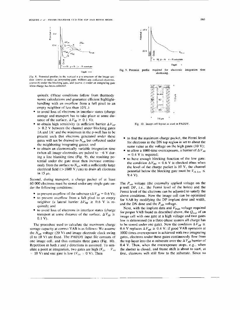
BOSIERS PI ( I / . : FRAME-TRANSFER CCD FOR ESP A N D MOVIE MODE 1063
- I
"N Sub
* Depth - n - SII p - SI 1 n -SI substrate
Depth - Fig. 9. Potential profile required for electronic integration time shortening.
Fig 8 . Potential profiles in the vertical n-p-n structure of the image sec- tion (curve a) under an integrating gate. without any collected electrons, (curve b) under the blocking gate, and (curve c ) under an integrating gate when charge has been collected --
quired); (These conditions follow from thermody- namic calculations and guarantee efficient highlight- handling with an overflow from a full pixel to an empty neighbor of less than 10% .) to avoid loss of electrons in interface states (charge storage and transport has to take place at some dis- tance of the surface, A Vse L 0.1 V); to obtain high sensitivity (a sufficient barrier A V,,, > 0.2 V between the channel under blocking gates IA and IA' and the minimum in the p-well has to be present such that electrons generated under these gates will not be drained to Naub but collected under the neighboring integrating gates); and to obtain an electronically variable integration time (when all image electrodes are pulsed to -6 V dur- ing a line blanking time (Fig. 9), the resulting po- tential under the gate must then increase continu- ously from the surface to N \ u h with a sufficiently large electrical field (> 1000 V /cm) to drain all electrons in 15 ps.
Second, during transport, a charge packet of at least 60 000 electrons must be stored under any single gate un- der the following conditions:
to prevent overflow of the substrate (A VAB = 0.6 V); to prevent overflow from a full pixel to an empty neighbor (a lateral barrier AV,, 2 0.6 V is re- quired); and to avoid loss of electrons in interface states (charge transport at some distance of the surface, A Vse 2
The procedure used to calculate the maximum charge storage capacity at correct VAB is as follows: We assume the Nsuh voltage (20 V) and image electrode clock swing (0 to 10 V) are fixed. The PADDY input file consists of one image cell, and thus contains three gates (Fig. IO). Repetition in both x and y directions is assumed. To sim- ulate a point at integration, two gates are high (V,, = V3, = 10 V) and one gate is low (VI, = 0 V). Then
0.1 V).
7.5 pm
Fig. IO. Image cell layout as used in PADDY.
to find the maximum charge packet, the Fermi level for electrons in the DN top region is set to about the same value as the voltage on the high gates (10 V); to allow a 1000-time overexposure, a barrier of A V , , = 0.4 V is required; to have enough blocking function of the low gate: the condition A V B B = 0.6 V is checked (thus when the level of the charge packet is 10 V, the channel potential below the blocking gate must be Vch.low I 9.4 V).
The Psuh voltage (the externally applied voltage on the p-well DP, i.e., the Fermi level of the holes) and the Fermi level of the electrons can be adjusted to satisfy the above conditions. Now the image cell can be optimized for VAB by modifying the DP implant dose and width, and the DN dose and the Psuh voltage.
Next, with the implant data and Vpsub voltage required for proper VAB found as described above, the Q,,, of an image cell with one gate at a high voltage and two gates low is determined (in a three-phase system all charge has to be stored under one gate). Now the condition A V,, 2 0.6 V replaces A V,, L 0.4 V: if good VAB operation at 1000 times overexposure is achieved with two integrating gates, electrons under these gates continuously flow from the top layer into the n-substrate over the A V , , barrier of 0.4 V. Then, when the overexposure stops, e.g., when the shutter is closed, and frame shift is about to start, at first, electrons will still flow to the substrate. Since no

I(M? IEEE TRANSACTIONS ON ELECTRON DEVICES, VOL. 38. NO. 5. MAY 1991
electrons are generated by light anymore, the potential of the neutral region in the n-type top player will rise; hence, AVAB increases and the flow of electrons will diminish and eventurally stop at A V,, = 0.6 V. The procedure is car- ried out for every gate, and the lowest capacity of the three gives the maximum charge capacity of an image cell.
The results give the required profiles for DP and DN, and the voltage for Psub.
From the 3-D potential simulations, one can also check the electronic shutter action by calculating the potential profile in the substrate when all image electrodes are at -6 V. The required profile is shown in Fig. 9. The min- imum electric field Emin from the channel to the substrate is 1000 V/cm.
C. Optimization of the Image Cell
t OR 1
Fig. 1 I . Connections of the SP channel stops to external P,,,, voltage.
TABLE 1 DESIGN VERSIONS WITH RESPECT TO THE SP I M P L A N T
SP SP QV Q W X
Dose Width R,, (SP) Paddy Version ( X I O ’ ? c m - ’ (pm) (MQ) (mV) (Electrons)
50 2 . 5 2 25 65 000 Since the image cell must not only perform an electrical a2 5 2 . 5 900 12 000 32 000
function, but also must yield an excellent quantum effi- b l 10 I .5 30 410 63 000 ciency of collected electrons versus incident photons, fur- b2 20 I .5 10 I40 ther optimization beyond Q,,, and VAB is required. b3 50 I .5 3 45 70000
1.1 5 70 7 6 0 0 0
a l
The highly doped SP channel stops hardly contribute to c 50 the spectral sensitivity of the sensor: most generated elec- trons recombine with the holes in the neutral layer or, at the bottom of the SP junction, are drained to the substrate by the electric field. Therefore, to obtain the highest pos- sible sensitivity, either the SP dose has to be reduced or the width has to be minimized.
However, to maintain a high-quality image under all circumstances, the resistance RSP of the channel stops has to be kept low: during (over)exposure, the generated holes are drained off by these stripes to the P s u b contact at the top of the image section (Fig. 11). Too large a voltage drop at overexposure will degrade the image quality, since the maximum charge-handling capacity will be reduced by the higher local SP stripe voltage. Given a certain ov- erexposure condition, this voltage drop and the resulting change in Q,,, can be easily estimated, since the program PADDY also gives the concentration of holes in the three different parts ( l A , 2A, and window) of the SP region. These concentrations can be used to calculate RSP, and hence to determine the voltage drop on these stripes oc- cumng during overexposure. Then a new calculation of Q,,, with the new local PIU,, voltage can be carried out. If this value differs too much from the original value, the lower signal will be seen in the image as a lower satura- tion output voltage below and above a highlight in the scene (“black smear”).
Reducing the implant dose of SP will result in depleted areas under the positive gates, which will significantly in- crease RSp Therefore, it is preferable to minimize the width rather than to reduce the implant dose. In a.first step, the effective outdiffusion is limited by the continu- ous DN well in which SP is implanted. Then the SP width was decreased from 2.5 to 1.5 pm and eventually 1.1 pm (implant widths).
A summary of the experimental designs to verify the influence of the SP dose and width is shown in Table I. Except for version a2, the DP implant widths for the im- age pixel were matched to maintain a good VAB and Q,,, condition.
The resistance R,, of one stripe was calculated as
L P Rsp = - . A
Using the expressions
P = Q / W 4 this yields
where
RSP Qi
is the resistance of SP stripe; is the number of holes in part of the SP region
(1 cell), as obtained from PADDY for one of the three regions (under the 1A gate (off), under the 2A gate (on), and in the window region (cf. Fig. 4));
is the length of part of SP stripe (in microm- eters);
is the number of cells (590); is the charge on one electron (in coulombs);
Li
nl- 4 plJ is the mobility of holes (400 cm2/V s);

BOSIERS er al . : FRAME-TRANSFER CCD FOR ESP AND MOVIE MODE I065
A
e,,, is the area of a cross section through an SP
stripe (in square micrometers); is the maximum charge packet in the image
pixel (neglecting the resistance of the SP stripes, i.e., with the external Phub voltage used in the calculations); and
A V(SP) is the voltage drop over the SP stripes with a total hole current per stripe corresponding to a 1000 times overexposure over one tenth of the image height (13.3 nA for this sensor) at the bottom of the image part (i.e., furthest away from the SP connec- tions, i.e., worst case).
D. Storage Cell
The minimum storage cell dimensions were originally calculated to achieve a charge-handling capacity about 15% higher than in the image section of version a1 (cf. Table I).
To illustrate the need for 3-D potential calculations rather than 2-D calculations, simulation results from PADDY and a 2-D version SEMMY for the calculation of the maximum charge-storage capacity are compared. The PADDY program gives the free-electron charge in a specified volume; the 2-D SEMMY program gives a charge density per unit length in the third dimension.
Fig. 12 shows the dimension of the cell after process- ing. The DN channel width is the implant width. Note that lateral isolation is performed by the p-well implant DP only, no SP is used: this maximizes the area available for charge storage.
The following calculations were performed and will be compared:
A 2-0 calculation over the height of the cell: This means a cross-section A-A' is considered. For the best estimate of Qmax, the result of the simulation along cross-section B-B' (see 2) below) was in- spected to find the width over which charge is stored. A 2-0 calculation over the width of the cell: Here, cross section B-B' was considered. To determine Q,,,, the similar approach as under 1) was fol- lowed. A 3-0 calculation over the whole cell: Here, a true 3-D simulation with PADDY was performed.
The results are summarized in Table 11. The measured values were found by adjusting the image electrodes such that no vertical antiblooming condition is reached. With the resulting larger charge packets from the image, the limiting storage capacity can be measured. Fig. 13 shows the extent of the charge packet as found with PADDY. Clearly, the effects around the corners become more im- portant with shrinking cell sizes and cannot be simulated
025 30 c1 A'
Fig. 12. Dimensions of the storage cell as used for PADDY and SEMMY.
I DN I
Fig. 13. Result of PADDY simulation of a full storage cell. Shown are the equipotential lines. Charge i s stored in an equi-potential volume within the inner contour line.
TABLE I1 COMPARISON OF 2-D A N D 3-D CALCULATION RESULTS
Maximum Charge Type of Calculation
SEMMY, height (A-A ') 96 000 SEMMY, width ( B - B ' ) 90 000 PADDY 13 000 Measured 17 000
efficiently by 2-D programs such as SEMMY. For more complicated structures such as the image cell (Fig. 4), a 2-D simulation would give completely unreliable results.
E. Serial Readout Registers For the intermediate readout registers, the requirements
were sufficient charge-handling capacity, high transport frequency, and very efficient charge transport both verti- cally and horizontally. Perfect transport across and along the three serial registers is essential to obtain a high-qual- ity image [7]. With the aid of the PADDY package, a structure was developed that allows excellent charge transport both horizontally and vertically at high frequen- cies under all circumstances (e.g., mask misalignments, processing tolerances, etc.).

1066 IEEE TRANSACTIONS ON ELECTRON DEVICES. VOL. 3X. NO. 5 . MAY 1991
In the first NTSC version of our sensor [2], we used projection-alignment equipment. Because of the larger possible misalignments between different mask layers, additional local self-aligned channel-stop and channel- well implants were essential in guaranteeing efficient transport through the readout registers. As an example, one stage of the vertical transport was illustrated in [2]. However, this new PAL sensor is produced using stepper lithography with a maximum alignment error between any two mask steps of less than 0.4 pm. Therefore, new 3-D PADDY calculations were performed taking into account the more accurate alignment. With minor changes in the layout, a design not requiring the additional channel-stop and channel-well implants-and thus saving two masks- could be realized.
VI. TECHNOLOGY
The devices were fabricated in a three-level polysilicon CCD process. No LOCOS is used. The 1-pm-deep n-channel CCD is fabricated in a 3-pm-deep p-well on an n on n+ epi substrate. Minimum dimensions used in pro- duction are 1.5 pm. Eleven masks are used, excluding color filters, which need two extra mask steps.
Cyan and yellow triplet color stripe filters are deposited on the wafers by a proprietary process. The overlap of both filters results in a green filter.
VII. MEASUREMENT RESULTS
Measurements show that the device completely satisfies the modeling results in both ESP- and movie-mode op- eration. In movie mode, frame transport through the in- termediate readout register to the storage section has no noticeable transfer inefficiency. The clock voltages for the transfer gates and the serial readout clocks required to achieve efficient charge transport correspond with the val- ues found from the 3-D potential calculations.
In ESP mode, given a correct dark current adjustment using the dark lines and the dark pixels per line, the image quality obtained in ESP mode by multiplexing the output signals from OR1 and OR2 is in no way inferior to the image obtained from OR2 only in movie mode.
Fig. 14 shows an image obtained from a resolution chart with a sensor operating in movie mode but not provided with color filters. By multiplexing the three outputs OT, OM, and OB up to 800 lines (H) can be clearly distin- guished.
All design versions were evaluated with respect to the “black smear” caused by the voltage drop over the SP’s. As could be expected from the RSP values from Table I, version a2 clearly suffered from this effect. This is illus- trated in Fig. 15. As can be clearly seen, the maximum charge packets are higher below and above the vertical grey scale than in evenly white areas: the higher the il- lumination on the SP stripes, the lower the resulting Q,,,.
Fig. 14. Image obtained from a sensor without color filters
Fig. 15. Image showing effect of too high resistance of channel stops
In the other versions, the effect on Q,,,, and hence satu- ration voltage was within the device specifications.
Fig. 16 shows the resolution obtained on a sensor pro- vided with color filters.
Fig. 17(a) shows a full-time image obtained in movie mode with an integration time of 1/50 s. Two consecu- tive fields were stored in a frame store. Since the scene contained a rotating disc, both the effect of long exposure times and the time delay between the integration of the two fields can be observed: the moving part of the scene is not sharp, and the “split image” caused by a delay of 20 ms between integration of the two fields can be ob- served. Fig. 17(b) shows the image obtained from the same scene under the same conditions, but with the sensor operating in ESP mode with an integration time of I / 1000 s: the short exposure time and the simultaneous integra-

BOSIERS er U / . : FRAME-TRANSFER CCD FOR ESP A N D MOVIE MODE 106i
Fig. 16. Image obtained from a sensor with color filters.
(b) Fig. 17. (a) Image obtained from a moving scene by combining two con- secutive fields with the sensor operating in movie mode. (b) Image obtained from a moving scene with the sensor operating in ESP mode.
400 500 600 700 E
Wavelength (nm) - Fig. 18. Quantum efficiency of the sensor for different widths of SP: A = 2.5 pm, B = 1.5 pn. C = 1.1 pm (implant widths): versions a l . b3. c.
TABLE 111 DEVICE SPECIFICATIONS
Dimensions Format Number of Pixels Pixel Size Number of Storage Cells Storage Cell Size Chip Size
Tcchnolog? CCD Structure
Gate Electrodes Minimum Dimensions Color Filters
ESP Mode Charge Reset Time Minimum Exp. Time Maximum Exp. Time Frame Flicker
Maximum Charge Clockswing
(image. storage. and readout clocks)
Readout Frequency
Sensitivity at Output Node Saturation at Output Voltage Output Amplifier Noise
(after CDS) (bandwidth: 200 kHz to 5 MHz)
Quantum Efficiency Dark Current Dynamic Range Overexposure Control
2 / 3 in 1170(H) x 5810‘) 7.5 pm(H) X 11.50 pm(V) Il70(H) x 2950‘) 7.5 p(H) x 9.25 pm(V) 10.09 mm x 10.51 mm
n-Channel in p-Well on n-Substrate Three-Level Polysilicon 1.5 pm Cyan-Green-Yellow Vertical Stripes
< 15 ps < 1 ms >200 ms < 0 . 5 %
60 000 electrons per cell I O v
22.5 MHz ( = 3 X 7.5 MHZ)
12 pV/electron 700 mV 17 electrons rms
> 15% at 400 nm: cf. Fig. 18 < I .O nA/cm’ at 60°C 1000: I > 1000 x saturation
tion of the two fields deliver a high-resolution picture free of artefacts.
Fig. 18 shows the photoresponsivity of the sensor (without color filters) for three widths of the channel stop in the image pixel (cf. Table I). As can clearly be seen, the quantum efficiency increases with decreasing SP width.
A summary of device specifications is given in Table 111, and a chip photograph is shown in Fig. 19.

Io68 IEEE TRANSACTIONS ON ELECTRON DEVICES. VOL. 38. NO. 5 . MAY 1991
obtained by performing 3-D potential simulations on all ciritical structures in the design. Thus the introduction of an intermediate readout register in no way compromised the overall performance of the device.
ACKNOWLEDGMENT The authors would like to thank their colleagues in the
CCD group and those responsible for camera electronics, color filters, testing, and assembly for their valuable con- tributions.
REFERENCES
[ 11 P. Kaiser, “Super-VHS specification for Europe.“ Fuiik.scliau, no. 6. Mar. 1988.
[2] J . Bosiers et al. “A 2/3” I 188(H) * 484(V) frame-transfer CCD for ESP and movie mode,” in IEDM Tech. Dig. (San Francisco). 1988, pp. 70-73.
131 J . Hynecek. “A new high-resolution I I-mm diagonal irnage sensor for still picture photography,” lEEE Trtrris. Elecrrori Dc,iic.c,.s. v o l . 36, no.
141 M . van der Steeg et al., “A frame-transfer CCD color imager with vertical antiblooniing,” lEEE T r m s . Electrorr D e i ~ i c ~ , . ~ . vol. ED-32. pp. 1430-1438, 1985.
(51 A. J . P. Theuwissen et U / . , “A 400K pixel 1 /2” accordion CCD- imager,” in lSSCC Dig. Tech. fnpers . Feb. 1988. pp. 48-49.
161 S. J . Polak et al.. “Semiconductor device modelling from the numer- ical point of view.” In/. J . Nurwrical Methock Engineering, vol. 24.
1 I , pp. 2466-2474, 1989.
Fig. 19. Chip photograph of the CCD image sensor.
VIII. CONCLUSIONS A high-resolution frame-transfer CCD that can operate
any deterioration in image quality was presented. This was
PP. 763-838, 1987.
ulation Semiconductor Devices Processes (Bologna. Italy). Sept. 1988.
171 J . Bisschop, “Computer simulations of parallel-to-series conversion in solid state frame transfer image sensors,” in Proc. 3rd / / I / . Cmf. S i n - according to both ESP and movie mode standards without
I