Embed Size (px)
Citation preview
HAL Id: hal-01735605https://hal.archives-ouvertes.fr/hal-01735605
Submitted on 16 Mar 2018
HAL is a multi-disciplinary open accessarchive for the deposit and dissemination of sci-entific research documents, whether they are pub-lished or not. The documents may come fromteaching and research institutions in France orabroad, or from public or private research centers.
L’archive ouverte pluridisciplinaire HAL, estdestinée au dépôt et à la diffusion de documentsscientifiques de niveau recherche, publiés ou non,émanant des établissements d’enseignement et derecherche français ou étrangers, des laboratoirespublics ou privés.
A 15 mV Inductorless Start-up Converter Using aPiezoelectric Transformer for Energy Harvesting
ApplicationsThomas Martinez, Gaël Pillonnet, François Costa
To cite this version:Thomas Martinez, Gaël Pillonnet, François Costa. A 15 mV Inductorless Start-up ConverterUsing a Piezoelectric Transformer for Energy Harvesting Applications. IEEE Transactions onPower Electronics, Institute of Electrical and Electronics Engineers, 2018, 33 (3), pp.2241-2253.10.1109/TPEL.2017.2690804. hal-01735605
Abstract—This paper presents an inductor-less start-up converter
for a sub-100 mV energy harvester based on an Armstrong
oscillator topology using a piezoelectric transformer and a
normally-on MOSFET. Two models of the converter have been
detailed and validated experimentally for the start-up phase and
steady-state operation to respectively determine the minimum
start-up input voltage and the voltage gain. The models have
been validated experimentally in a set-up associating the
converter and a thermo-electric generator. Based on a Rosen-
type piezoelectric transformer and off-the-shelf components, the
proposed start-up topology begins to oscillate at 15 mV and
achieves a 1 V output voltage at only 43 mV. Compared to the
literature, the topology needs no inductive component and
achieves self-starting operation with a smaller input voltage.
Index Terms—start-up converter, Armstrong oscillator,
piezoelectric transformer, energy harvesting, cold-start
I. INTRODUCTION
THE progress in the scaling of micro-electronic devices and
the reduction of their energy consumption have contributed to
the development of low-power portable systems. For wireless
sensor nodes or implantable device applications, batteries are
unsuitable as they have a limited lifetime and may need
maintenance and to be replaced [1]. For these low power
applications, it is more interesting to be supplied by a
completely autonomous system by harvesting the ambient
energy. This makes it possible to develop “deploy and forget”
sensor nodes that will not need any maintenance or
replacement after they are installed and can work for several
years. Several energy sources can be harvested such as light,
heat, mechanical vibrations, electromagnetic radiations and
chemical energy from bacteria reactions [2]. Among those
possibilities, thermo-electric generators (TEG) and rectennas
[3] provide DC voltages from thermal and electromagnetic
energy harvesting, respectively. In most applications, the TEG
provides ultra-low voltage (<100 mV) but has a low internal
resistance (< 10 Ω) while the rectenna has an internal
resistance in the range of 100 Ω to a couple of kΩ [3].
However, they both constitute interesting solutions for
T. Martinez is with the laboratory SATIE (Systems & Applications of
Information & Energy Technologies), ENS Cachan, 91120 Cachan, France.
G. Pillonnet is with the University of Grenoble Alpes, Grenoble 38000,
France, and also with the CEA, Leti-MINATEC Campus, Grenoble 38054,France (e-mail: [email protected]).
F. Costa is with the University Paris-Est-Créteil (UPEC), Créteil 94000,
France and also with the laboratory SATIE (Systems & Applications of Information & Energy Technologies), ENS Cachan, 91120 Cachan, France
applications which consume less than a few hundred
microwatts.
The voltages provided by energy harvesters strongly depend
on the ambient conditions and they must be adapted in order to
supply the load. An interface circuit is needed to step-up the
voltage, track the maximal power, store the energy and supply
the node sensor at maximum efficiency. Classical switched-
mode DC-DC converters already achieve these functions [4]
[5].
An additional specific constraint inherent to energy
harvesting is the “cold start”, i.e. to start the circuit when the
storage element is fully discharged. When the voltage supplied
by the harvester is lower than the threshold voltage of the
transistors used in the switched-mode converter, the system
cannot start and step-up the harvester output voltage. Many
papers avoid this issue by assuming an initial energy is
provided to the circuit by the storage element [6] but this is
not suitable for applications after long standby periods.
The architecture of the proposed solution is presented in
Fig. 1. A start-up converter is added to the circuit which acts
as an intermittent supply. In fact, it must start at the voltage
provided by the harvester when the battery is discharged, step-
up the harvester output voltage and initially charge a storage
capacitor. The main constraint of the start-up converter is to
start at the voltage provided by the harvester which may be
lower than 100 mV and to step-up the output voltage high
enough in order to supply the drive of the main DC-DC
converter. Its power efficiency is therefore not the most
important parameter. When Cstart has reached a sufficient
voltage, the energy stored will then supply the optimized main
converter whose main focus is efficiency.
Fig. 1: Overall architecture of the conversion circuit
Several low start-up voltage converters have been proposed.
Some systems use classical switched mode architectures while
focusing on lowering the threshold-voltage of the transistors
whereas other fabrication process with low threshold voltage
Thomas Martinez, Gaël Pillonnet, Member IEEE, François Costa, Member IEEE
A 15 mV Inductorless Start-up Converter Using
a Piezoelectric Transformer for Energy
Harvesting Applications
transistors [7] can be used or forward body-biasing [8]. The
use of a charge pump with depletion-mode transistors has also
been proposed [9]. Here, these converters are still limited by
the threshold voltage of the transistors but has difficulty
starting at voltages lower than 100 mV. Reference [10]
proposes a boost converter activated by a mechanical switch
that starts at 35 mV but this needs an external vibration that is
not always available. Other low voltage start-up converters
consist of resonant step-up oscillators such as the Armstrong
Oscillator architecture based on a magnetic transformer and an
amplifying element [11]. In [12], the converter uses this
architecture to start from a TEG source at voltages as low as
40 mV. In [13],the Armstrong oscillator is also used to start
from an RF source from a 100 mV input voltage. Several
transformers can be cascaded to achieve a start-up voltage as
low as 6 mV [14]. All those propositions have the
inconvenience of being implemented with magnetic
transformers. In [15] and [16], ultra-low voltage resonant
oscillators are combined with a charge pump converter to start
at voltages as low as 10 mV and 100 mV, respectively, but
they also use a bulky inductance to realize the conversion.
Furthermore, most of these solutions are only compatible with
harvesters with a low internal resistance such as a TEG (< 10
Ω).
The use of resonant oscillators enables a low start-up
voltage to be obtained but the magnetic transformers and
inductors are bulky elements that increase the size of the
converter and are difficult to shrink and integrate with micro-
electronic techniques. However, piezoelectric transformers
(PT’s) constitute an interesting alternative to magnetic ones.
They are notably used as power converters for cold cathode
fluorescent lamps used in liquid crystal displays (LCD’s) [17].
They may exhibit higher voltage gain and power density than
magnetic transformers and a quality factor as high as 1000
[18]. Furthermore, their use in power converters allows the
electromagnetic radiation of the system to be limited [19]. The
relative high Curie temperature (> 200°C) of certain ceramic
elements may also allow PT’s to work at higher temperatures
than a magnetic element [20]. Their integration on silicon has
already been realized and their compatibility with classical
microelectronic fabrication processes demonstrated [21].
Reference [22] presents a start-up converter based on a
resonant oscillator using a PT with start-up voltages of 69 mV
for an inductor-less circuit but it is only suitable for low
internal resistance harvesters, or coupled to an inductor [23].
In this paper, a self-start-up converter based on an
Armstrong oscillator using a PT and a “biasing element”, i.e. a
resistor, replacing the magnetic transformer is presented. The
objective is that the circuit self-starts using the voltage
provided by the harvester whether it is a TEG, rectenna or
biofuel cell, and to step it up at to a voltage sufficiently high to
start the main converter. The proposed circuit is completely
inductorless, does not generate any electromagnetic
interference and could work at high temperatures and have the
potential to be integrated more easily in a microelectronic
process flow. The circuit has been modeled in both start-up
phase and steady state which has allowed the start-up voltage
and output voltage of the converter to be determined,
respectively. These models were then validated through a
time-domain simulation. The converter has been fabricated on
a printed circuit board (PCB) in order to validate the
simulation results. This paper describes the electrical
characteristics of the PT and the behavior of the converter in
section II. The models of the circuit are then described in
section III. Then, the experimental realization and
measurements are presented in section IV. Finally, we
compare the results obtained with the analytical models, the
simulation and experimental measurements before discussing
the performances and the design trade-off of this novel start-
up converter.
II. START-UP CONVERTER TOPOLOGY BASED ON
PIEZOELECTRIC TRANSFORMER
A. Piezoelectric Transformer
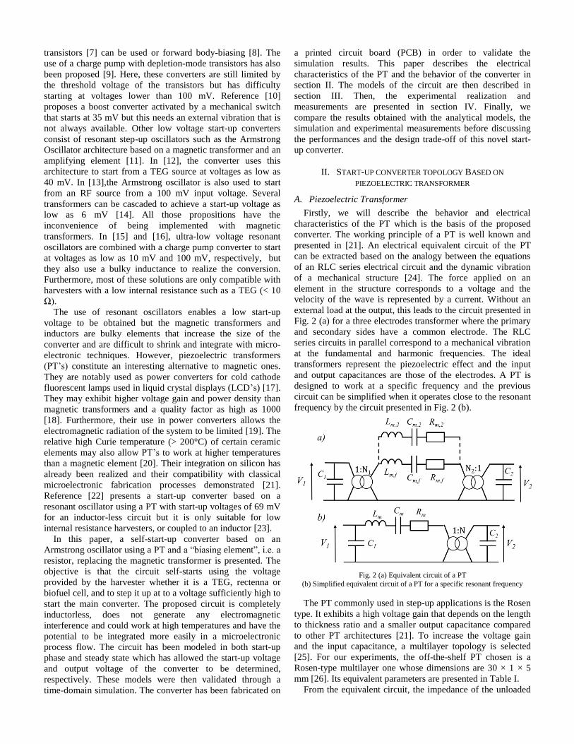
Firstly, we will describe the behavior and electrical
characteristics of the PT which is the basis of the proposed
converter. The working principle of a PT is well known and
presented in [21]. An electrical equivalent circuit of the PT
can be extracted based on the analogy between the equations
of an RLC series electrical circuit and the dynamic vibration
of a mechanical structure [24]. The force applied on an
element in the structure corresponds to a voltage and the
velocity of the wave is represented by a current. Without an
external load at the output, this leads to the circuit presented in
Fig. 2 (a) for a three electrodes transformer where the primary
and secondary sides have a common electrode. The RLC
series circuits in parallel correspond to a mechanical vibration
at the fundamental and harmonic frequencies. The ideal
transformers represent the piezoelectric effect and the input
and output capacitances are those of the electrodes. A PT is
designed to work at a specific frequency and the previous
circuit can be simplified when it operates close to the resonant
frequency by the circuit presented in Fig. 2 (b).
Fig. 2 (a) Equivalent circuit of a PT
(b) Simplified equivalent circuit of a PT for a specific resonant frequency
The PT commonly used in step-up applications is the Rosen
type. It exhibits a high voltage gain that depends on the length
to thickness ratio and a smaller output capacitance compared
to other PT architectures [21]. To increase the voltage gain
and the input capacitance, a multilayer topology is selected
[25]. For our experiments, the off-the-shelf PT chosen is a
Rosen-type multilayer one whose dimensions are 30 × 1 × 5
mm [26]. Its equivalent parameters are presented in Table I.
From the equivalent circuit, the impedance of the unloaded
PT seen from the input is equal to:
𝑍𝑃𝑇,1 =
𝑅𝑚 + 𝑗 (𝐿𝑚𝜔 −1
𝐶𝑒𝑞𝜔)
1 + 𝑗𝐶1𝜔(𝑅𝑚 + 𝑗 (𝐿𝑚𝜔 −1
𝐶𝑒𝑞𝜔))
(1)
where 𝐶𝑒𝑞 =𝐶𝑚.𝑁
2.𝐶2
𝐶𝑚+𝑁2.𝐶2
is the equivalent capacitance when
the output capacitance C2 is reported back in the RLC series
circuit.
The main parameters of our PT are given in Table. I. The
impedance curve measured at the input of the unloaded PT
shows two resonances. The first and second ones corresponds
to the series and parallel resonant frequency respectively and
can be expressed as:
where 𝐶𝑒𝑞,𝑖𝑛 =𝐶𝑒𝑞.𝐶1
𝐶𝑒𝑞+𝐶1.
In our start-up converter, a capacitive load Cload is
structurally added at the output of the PT in parallel with C2
(see later in Fig. 4). This capacitance Cload is due to the
internal capacitance of the elements at the output of the PT in
our topology (diode, transistors). The output capacitance is
then Cout=C2+Cload and the Ceq value changes with Cout
replacing C2. The resonant frequencies are then switched to
lower ones. The capacitive load Cload also has an impact on the
voltage gain of the PT. The voltage gain V2/V1 is given by:
𝐺𝑃𝑇 =𝑉2𝑉1=
1
𝑁𝑗𝐶𝑜𝑢𝑡𝜔(𝑅𝑚 + 𝑗 (𝐿𝑚𝜔 −1
𝐶𝑒𝑞𝜔))
(3)
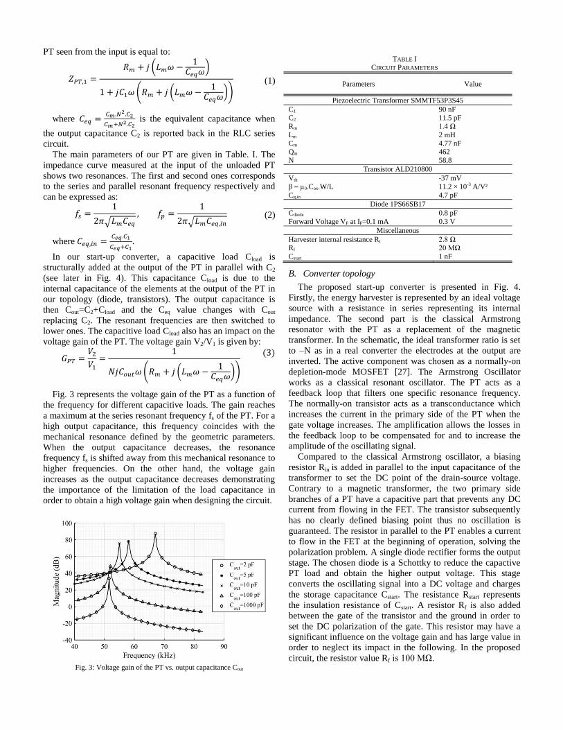
Fig. 3 represents the voltage gain of the PT as a function of
the frequency for different capacitive loads. The gain reaches
a maximum at the series resonant frequency fs of the PT. For a
high output capacitance, this frequency coincides with the
mechanical resonance defined by the geometric parameters.
When the output capacitance decreases, the resonance
frequency fs is shifted away from this mechanical resonance to
higher frequencies. On the other hand, the voltage gain
increases as the output capacitance decreases demonstrating
the importance of the limitation of the load capacitance in
order to obtain a high voltage gain when designing the circuit.
Fig. 3: Voltage gain of the PT vs. output capacitance Cout
TABLE I CIRCUIT PARAMETERS
Parameters Value
Piezoelectric Transformer SMMTF53P3S45
C1 90 nF
C2 11.5 pF
Rm 1.4 Ω
Lm Cm
2 mH 4.77 nF
Qm 462
N 58,8
Transistor ALD210800
Vth -37 mV
β = µ0.Cox.W/L 11.2 × 10⁻³ A/V²
Cg,in 4.7 pF
Diode 1PS66SB17
Cdiode 0.8 pF
Forward Voltage VF at IF=0.1 mA 0.3 V
Miscellaneous
Harvester internal resistance Rt 2.8 Ω Rf 20 MΩ
Cstart 1 nF
B. Converter topology
The proposed start-up converter is presented in Fig. 4.
Firstly, the energy harvester is represented by an ideal voltage
source with a resistance in series representing its internal
impedance. The second part is the classical Armstrong
resonator with the PT as a replacement of the magnetic
transformer. In the schematic, the ideal transformer ratio is set
to –N as in a real converter the electrodes at the output are
inverted. The active component was chosen as a normally-on
depletion-mode MOSFET [27]. The Armstrong Oscillator
works as a classical resonant oscillator. The PT acts as a
feedback loop that filters one specific resonance frequency.
The normally-on transistor acts as a transconductance which
increases the current in the primary side of the PT when the
gate voltage increases. The amplification allows the losses in
the feedback loop to be compensated for and to increase the
amplitude of the oscillating signal.
Compared to the classical Armstrong oscillator, a biasing
resistor Rin is added in parallel to the input capacitance of the
transformer to set the DC point of the drain-source voltage.
Contrary to a magnetic transformer, the two primary side
branches of a PT have a capacitive part that prevents any DC
current from flowing in the FET. The transistor subsequently
has no clearly defined biasing point thus no oscillation is
guaranteed. The resistor in parallel to the PT enables a current
to flow in the FET at the beginning of operation, solving the
polarization problem. A single diode rectifier forms the output
stage. The chosen diode is a Schottky to reduce the capactive
PT load and obtain the higher output voltage. This stage
converts the oscillating signal into a DC voltage and charges
the storage capacitance Cstart. The resistance Rstart represents
the insulation resistance of Cstart. A resistor Rf is also added
between the gate of the transistor and the ground in order to
set the DC polarization of the gate. This resistor may have a
significant influence on the voltage gain and has large value in
order to neglect its impact in the following. In the proposed
circuit, the resistor value Rf is 100 MΩ.
𝑓𝑠 =1
2𝜋√𝐿𝑚𝐶𝑒𝑞, 𝑓𝑝 =
1
2𝜋√𝐿𝑚𝐶𝑒𝑞,𝑖𝑛 (2)
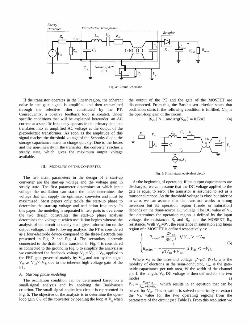
Fig. 4: Circuit Schematic
If the transistor operates in the linear region, the inherent
noise in the gate signal is amplified and then transmitted
through the selective filter constituted by the PT.
Consequently, a positive feedback loop is created. Under
specific conditions that will be explained hereunder, an AC
current at a specific frequency appears in the primary side that
translates into an amplified AC voltage at the output of the
piezoelectric transformer. As soon as the amplitude of this
signal reaches the threshold voltage of the Schottky diode, the
storage capacitance starts to charge quickly. Due to the losses
and the non-linearity in the transistor, the converter reaches a
steady state, which gives the maximum output voltage
available.
III. MODELING OF THE CONVERTER
The two main parameters in the design of a start-up
converter are the start-up voltage and the voltage gain in
steady state. The first parameter determines at which input
voltage the oscillation can start; the latter determines the
voltage that will supply the optimized converter and must be
maximized. Most papers only tackle the start-up phase to
determine the start-up voltage and oscillation frequency. In
this paper, the modeling is separated in two parts to overcome
the two design constraints: the start-up phase analysis
determines the voltage at which oscillation begins whereas the
analysis of the circuit in steady state gives information on the
output voltage. In the following analysis, the PT is considered
as a four-electrode device compared to the three-electrode one
presented in Fig. 2 and Fig. 4. The secondary electrode
connected to the drain of the transistor in Fig. 4 is considered
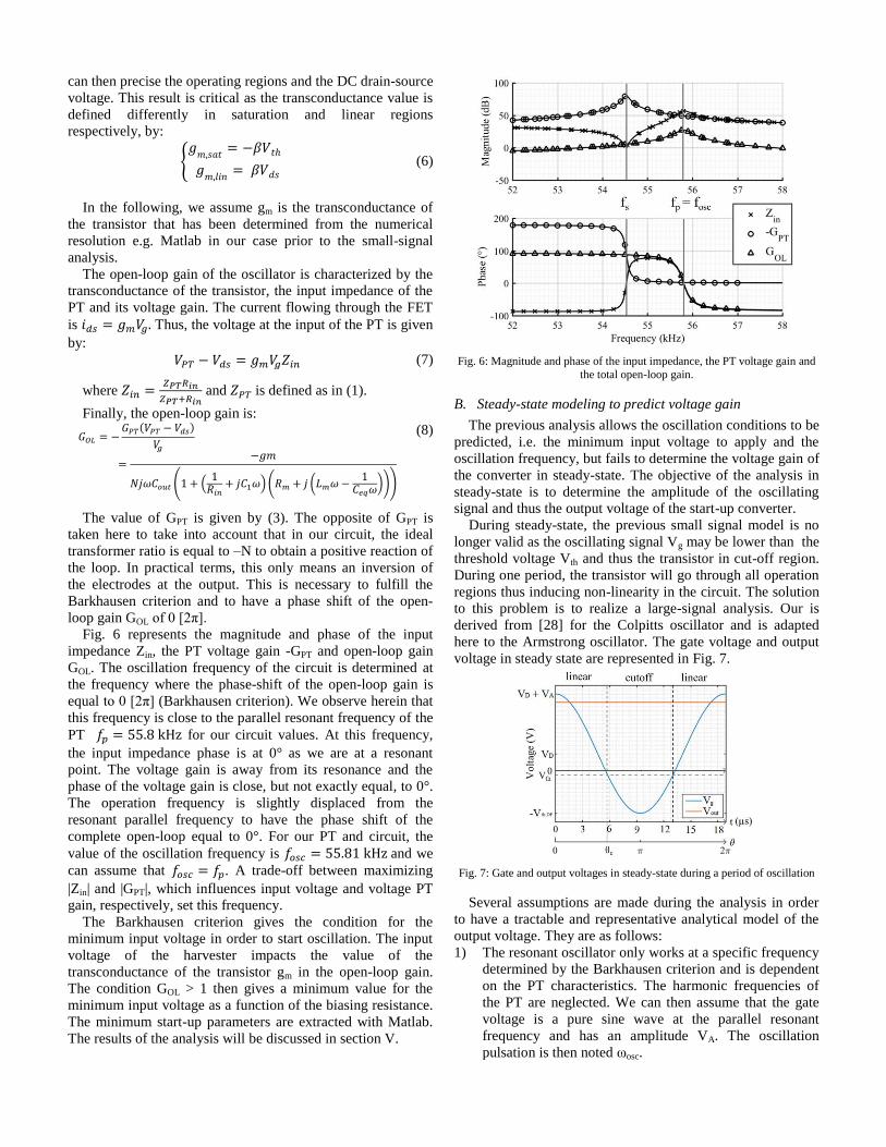
as connected to the ground in Fig. 5 to simplify the analysis as
we considered the feedback voltage Vg = Vds + VC2 applied to
the FET gate governed mainly by VC2 and not by the signal
Vds as VC2>>Vds due to the inherent high voltage gain of the
PT.
A. Start-up phase modeling
The oscillation condition can be determined based on a
small-signal analysis and by applying the Barkhausen
criterion. The small-signal equivalent circuit is represented in
Fig. 5. The objective of the analysis is to determine the open-
loop gain GOL of the converter by opening the loop at Vg when
the output of the PT and the gate of the MOSFET are
disconnected. From this, the Barkhausen criterion states that
oscillation starts if the following condition is fulfilled, GOL is
the open-loop gain of the circuit:
|𝐺𝑂𝐿| > 1 and arg(𝐺𝑂𝐿) = 0 [2𝜋] (4)
Fig. 5: Small-signal equivalent circuit
At the beginning of operation, if the output capacitances are
discharged, we can assume that the DC voltage applied to the
gate is equal to zero. The transistor is assumed to act as a
transconductance. As the threshold voltage is close but inferior
to zero, we can assume that the transistor works in strong
inversion but its operation region (triode or saturation)
depends on the drain-source DC voltage. The DC value of Vds
that determines the operation region is defined by the input
voltage, the resistances Rt and Rin and the MOSFET Ron
resistance. With Vgs=0V, the resistance in saturation and linear
region of a MOSFET is defined respectively as:
𝑅𝑜𝑛,𝑠𝑎𝑡 =2𝑉𝑑𝑠
𝛽𝑉𝑡ℎ 2 𝑖𝑓 𝑉𝑑𝑠 > −𝑉𝑡ℎ
𝑅𝑜𝑛,𝑙𝑖𝑛 = −2
𝛽(𝑉𝑡ℎ + 𝑉𝑑𝑠) 𝑖𝑓 𝑉𝑑𝑠 < −𝑉𝑡ℎ
(5)
Where Vth is the threshold voltage, 𝛽=𝜇𝐶𝑜𝑥𝑊/𝐿; μ is the
mobility of electrons in the semi-conductor, Cox is the gate-
oxide capacitance per unit area, W the width of the channel
and L the length. Vds DC voltage is then defined for the two
modes as
𝑉𝑑𝑠 =𝑅𝑜𝑛.𝑉𝑖𝑛
𝑅𝑜𝑛+𝑅𝑡+𝑅𝑖𝑛 , which results in an equation that can be
solved for Vds. This equation is solved numerically to extract
the Vds value for the two operating regions from the
parameters of the circuit (see Table I). From this resolution we
can then precise the operating regions and the DC drain-source
voltage. This result is critical as the transconductance value is
defined differently in saturation and linear regions
respectively, by:
In the following, we assume gm is the transconductance of
the transistor that has been determined from the numerical
resolution e.g. Matlab in our case prior to the small-signal
analysis.
The open-loop gain of the oscillator is characterized by the
transconductance of the transistor, the input impedance of the
PT and its voltage gain. The current flowing through the FET
is 𝑖𝑑𝑠 = 𝑔𝑚𝑉𝑔. Thus, the voltage at the input of the PT is given
by:
where 𝑍𝑖𝑛 =𝑍𝑃𝑇𝑅𝑖𝑛
𝑍𝑃𝑇+𝑅𝑖𝑛 and 𝑍𝑃𝑇 is defined as in (1).
Finally, the open-loop gain is:
𝐺𝑂𝐿 = −𝐺𝑃𝑇(𝑉𝑃𝑇 − 𝑉𝑑𝑠)
𝑉𝑔
=−𝑔𝑚
𝑁𝑗𝜔𝐶𝑜𝑢𝑡 (1 + (1𝑅𝑖𝑛
+ 𝑗𝐶1𝜔)(𝑅𝑚 + 𝑗 (𝐿𝑚𝜔−1
𝐶𝑒𝑞𝜔)))
(8)
The value of GPT is given by (3). The opposite of GPT is
taken here to take into account that in our circuit, the ideal
transformer ratio is equal to –N to obtain a positive reaction of
the loop. In practical terms, this only means an inversion of
the electrodes at the output. This is necessary to fulfill the
Barkhausen criterion and to have a phase shift of the open-
loop gain GOL of 0 [2π].
Fig. 6 represents the magnitude and phase of the input
impedance Zin, the PT voltage gain -GPT and open-loop gain
GOL. The oscillation frequency of the circuit is determined at
the frequency where the phase-shift of the open-loop gain is
equal to 0 [2π] (Barkhausen criterion). We observe herein that
this frequency is close to the parallel resonant frequency of the
PT 𝑓𝑝 = 55.8 kHz for our circuit values. At this frequency,
the input impedance phase is at 0° as we are at a resonant
point. The voltage gain is away from its resonance and the
phase of the voltage gain is close, but not exactly equal, to 0°.
The operation frequency is slightly displaced from the
resonant parallel frequency to have the phase shift of the
complete open-loop equal to 0°. For our PT and circuit, the
value of the oscillation frequency is 𝑓𝑜𝑠𝑐 = 55.81 kHz and we
can assume that 𝑓𝑜𝑠𝑐 = 𝑓𝑝. A trade-off between maximizing
|Zin| and |GPT|, which influences input voltage and voltage PT
gain, respectively, set this frequency.
The Barkhausen criterion gives the condition for the
minimum input voltage in order to start oscillation. The input
voltage of the harvester impacts the value of the
transconductance of the transistor gm in the open-loop gain.
The condition GOL > 1 then gives a minimum value for the
minimum input voltage as a function of the biasing resistance.
The minimum start-up parameters are extracted with Matlab.
The results of the analysis will be discussed in section V.
Fig. 6: Magnitude and phase of the input impedance, the PT voltage gain and
the total open-loop gain.
B. Steady-state modeling to predict voltage gain
The previous analysis allows the oscillation conditions to be
predicted, i.e. the minimum input voltage to apply and the
oscillation frequency, but fails to determine the voltage gain of
the converter in steady-state. The objective of the analysis in
steady-state is to determine the amplitude of the oscillating
signal and thus the output voltage of the start-up converter.
During steady-state, the previous small signal model is no
longer valid as the oscillating signal Vg may be lower than the
threshold voltage Vth and thus the transistor in cut-off region.
During one period, the transistor will go through all operation
regions thus inducing non-linearity in the circuit. The solution
to this problem is to realize a large-signal analysis. Our is
derived from [28] for the Colpitts oscillator and is adapted
here to the Armstrong oscillator. The gate voltage and output
voltage in steady state are represented in Fig. 7.
Fig. 7: Gate and output voltages in steady-state during a period of oscillation
Several assumptions are made during the analysis in order
to have a tractable and representative analytical model of the
output voltage. They are as follows:
1) The resonant oscillator only works at a specific frequency
determined by the Barkhausen criterion and is dependent
on the PT characteristics. The harmonic frequencies of
the PT are neglected. We can then assume that the gate
voltage is a pure sine wave at the parallel resonant
frequency and has an amplitude VA. The oscillation
pulsation is then noted ωosc.
𝑔𝑚,𝑠𝑎𝑡
= −𝛽𝑉𝑡ℎ
𝑔𝑚,𝑙𝑖𝑛
= 𝛽𝑉𝑑𝑠 (6)
𝑉𝑃𝑇 − 𝑉𝑑𝑠 = 𝑔𝑚𝑉𝑔𝑍𝑖𝑛 (7)
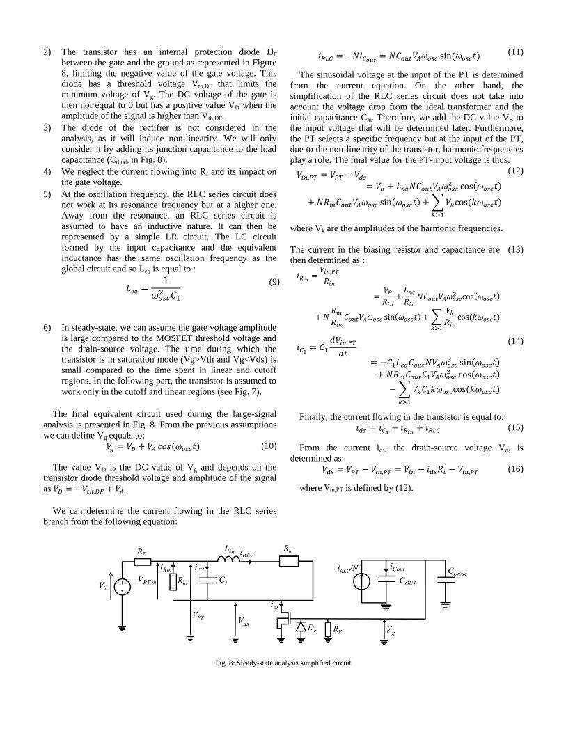
2) The transistor has an internal protection diode DF
between the gate and the ground as represented in Figure
8, limiting the negative value of the gate voltage. This
diode has a threshold voltage Vth,DF that limits the
minimum voltage of Vg. The DC voltage of the gate is
then not equal to 0 but has a positive value VD when the
amplitude of the signal is higher than Vth,DF.
3) The diode of the rectifier is not considered in the
analysis, as it will induce non-linearity. We will only
consider it by adding its junction capacitance to the load
capacitance (Cdiode in Fig. 8).
4) We neglect the current flowing into Rf and its impact on
the gate voltage.
5) At the oscillation frequency, the RLC series circuit does
not work at its resonance frequency but at a higher one.
Away from the resonance, an RLC series circuit is
assumed to have an inductive nature. It can then be
represented by a simple LR circuit. The LC circuit
formed by the input capacitance and the equivalent
inductance has the same oscillation frequency as the
global circuit and so Leq is equal to :
𝐿𝑒𝑞 =1
𝜔𝑜𝑠𝑐2 𝐶1
(9)
6) In steady-state, we can assume the gate voltage amplitude
is large compared to the MOSFET threshold voltage and
the drain-source voltage. The time during which the
transistor is in saturation mode (Vg>Vth and Vg<Vds) is
small compared to the time spent in linear and cutoff
regions. In the following part, the transistor is assumed to
work only in the cutoff and linear regions (see Fig. 7).
The final equivalent circuit used during the large-signal
analysis is presented in Fig. 8. From the previous assumptions
we can define Vg equals to:
𝑉𝑔 = 𝑉𝐷 + 𝑉𝐴 𝑐𝑜𝑠(𝜔𝑜𝑠𝑐𝑡) (10)
The value VD is the DC value of Vg and depends on the
transistor diode threshold voltage and amplitude of the signal
as 𝑉𝐷 = −𝑉𝑡ℎ,𝐷𝐹 + 𝑉𝐴.
We can determine the current flowing in the RLC series
branch from the following equation:
𝑖𝑅𝐿𝐶 = −𝑁𝑖𝐶𝑜𝑢𝑡 = 𝑁𝐶𝑜𝑢𝑡𝑉𝐴𝜔𝑜𝑠𝑐 sin(𝜔𝑜𝑠𝑐𝑡) (11)
The sinusoidal voltage at the input of the PT is determined
from the current equation. On the other hand, the
simplification of the RLC series circuit does not take into
account the voltage drop from the ideal transformer and the
initial capacitance Cm. Therefore, we add the DC-value VB to
the input voltage that will be determined later. Furthermore,
the PT selects a specific frequency but at the input of the PT,
due to the non-linearity of the transistor, harmonic frequencies
play a role. The final value for the PT-input voltage is thus:
𝑉𝑖𝑛,𝑃𝑇 = 𝑉𝑃𝑇 − 𝑉𝑑𝑠= 𝑉𝐵 + 𝐿𝑒𝑞𝑁𝐶𝑜𝑢𝑡𝑉𝐴𝜔𝑜𝑠𝑐
2 cos(𝜔𝑜𝑠𝑐𝑡)
+ 𝑁𝑅𝑚𝐶𝑜𝑢𝑡𝑉𝐴𝜔𝑜𝑠𝑐 sin(𝜔𝑜𝑠𝑐𝑡) +∑𝑉𝑘cos (𝑘𝜔𝑜𝑠𝑐𝑡)
𝑘>1
(12)
where Vk are the amplitudes of the harmonic frequencies.
The current in the biasing resistor and capacitance are
then determined as :
𝑖𝑅𝑖𝑛 =𝑉𝑖𝑛,𝑃𝑇𝑅𝑖𝑛
=𝑉𝐵𝑅𝑖𝑛
+𝐿𝑒𝑞
𝑅𝑖𝑛𝑁𝐶𝑜𝑢𝑡𝑉𝐴𝜔𝑜𝑠𝑐
2 cos(𝜔𝑜𝑠𝑐𝑡)
+ 𝑁𝑅𝑚𝑅𝑖𝑛
𝐶𝑜𝑢𝑡𝑉𝐴𝜔𝑜𝑠𝑐 sin(𝜔𝑜𝑠𝑐𝑡) +∑𝑉𝑘𝑅𝑖𝑛
cos (𝑘𝜔𝑜𝑠𝑐𝑡)
𝑘>1
(13)
𝑖𝐶1 = 𝐶1𝑑𝑉𝑖𝑛,𝑃𝑇𝑑𝑡
= −𝐶1𝐿𝑒𝑞𝐶𝑜𝑢𝑡𝑁𝑉𝐴𝜔𝑜𝑠𝑐3 sin(𝜔𝑜𝑠𝑐𝑡)
+ 𝑁𝑅𝑚𝐶𝑜𝑢𝑡𝐶1𝑉𝐴𝜔𝑜𝑠𝑐2 cos(𝜔𝑜𝑠𝑐𝑡)
−∑𝑉𝑘𝐶1𝑘𝜔𝑜𝑠𝑐cos (𝑘𝜔𝑜𝑠𝑐𝑡)
𝑘>1
(14)
Finally, the current flowing in the transistor is equal to:
𝑖𝑑𝑠 = 𝑖𝐶1 + 𝑖𝑅𝑖𝑛 + 𝑖𝑅𝐿𝐶 (15)
From the current ids, the drain-source voltage Vds is
determined as:
𝑉𝑑𝑠 = 𝑉𝑃𝑇 − 𝑉𝑖𝑛,𝑃𝑇 = 𝑉𝑖𝑛 − 𝑖𝑑𝑠𝑅𝑡 − 𝑉𝑖𝑛,𝑃𝑇 (16)
where Vin,PT is defined by (12).
Fig. 8: Steady-state analysis simplified circuit
For the classical transistor model and considering
assumption 6, we have:
𝑖𝑑𝑠,𝑐𝑢𝑡𝑜𝑓𝑓 = 0 if 𝑉𝑔 < 𝑉𝑡
𝑖𝑑𝑠,𝑙𝑖𝑛𝑒𝑎𝑟 = 𝛽(2(𝑉𝑔 − 𝑉𝑡ℎ) − 𝑉𝑑𝑠)𝑉𝑑𝑠 if 𝑉𝑔 > 𝑉𝑡
(17)
During a period of steady-state oscillation, the transistor
will switch operating region when Vg>Vth. We define 𝜃 =𝜔𝑜𝑠𝑐𝑡 and 𝜃𝑐 = 𝜔𝑜𝑠𝑐𝑡𝑐 as the angle at which the change of
region takes place (fig.8). At the boundary between the two
operating regions, we have 𝑉𝑔,𝑐 = 𝑉𝑡ℎ which leads to
cos (𝜃𝑐) =𝑉𝑡ℎ − 𝑉𝐷𝑉𝐴
(18)
The current flowing through the transistor is periodic with a
fundamental pulsation ωosc. It can thus be represented by a
Fourier series such as:
𝑖𝑑𝑠 = 𝑖𝑑𝑠,𝐷𝐶 +∑𝑖𝑑𝑠,𝑖cos(𝑘𝜔𝑜𝑠𝑐𝑡)
𝑘≥1
(19)
The values of ids,k and ids,DC are then defined using the
formula for Fourier coefficients and the current equation:
𝑖𝑑𝑠,𝐷𝐶 =1
2𝜋∫ 𝑖𝑑𝑠𝑑𝜃2𝜋
0
=𝛽
𝜋∫ 𝑉𝑑𝑠(2(𝑉𝑔 − 𝑉𝑡ℎ) − 𝑉𝑑𝑠)𝑑𝜃 𝜃𝑐
0
(20)
𝑖𝑑𝑠,𝑘 =1
𝜋∫ 𝑖𝑑𝑠 cos(𝑘𝜃) 𝑑𝜃2𝜋
0
=2𝛽
𝜋∫ 𝑉𝑑𝑠 cos(𝑘𝜃) (2(𝑉𝑔 − 𝑉𝑡ℎ) − 𝑉𝑑𝑠)𝑑𝜃 𝜃𝑐
0
(21)
In (21) and (22), the Fourier coefficients of ids are
determined by the equations of the transistor. Those
coefficients are also defined by equation (16) and the values of
𝑖𝑅𝑖𝑛 , 𝑖𝐶1 and 𝑖𝑅𝐿𝐶 determined in (12), (14) and (15). If, in the
analysis, we consider n-1 harmonics, the equalization of those
coefficients results in a system of n+1 equations with n+1
unknowns. The equations correspond to the DC value, the
fundamental coefficient and the n-1 harmonics. The unknowns
are the value of the cutoff angle 𝜃𝑐, the DC value VB of Vin
and the values of Vk. VA can be extracted from 𝜃𝑐. As it is
only interesting to determine VB and 𝜃𝑐, we just consider the
system composed of the two equations for the DC and
fundamental values of ids.
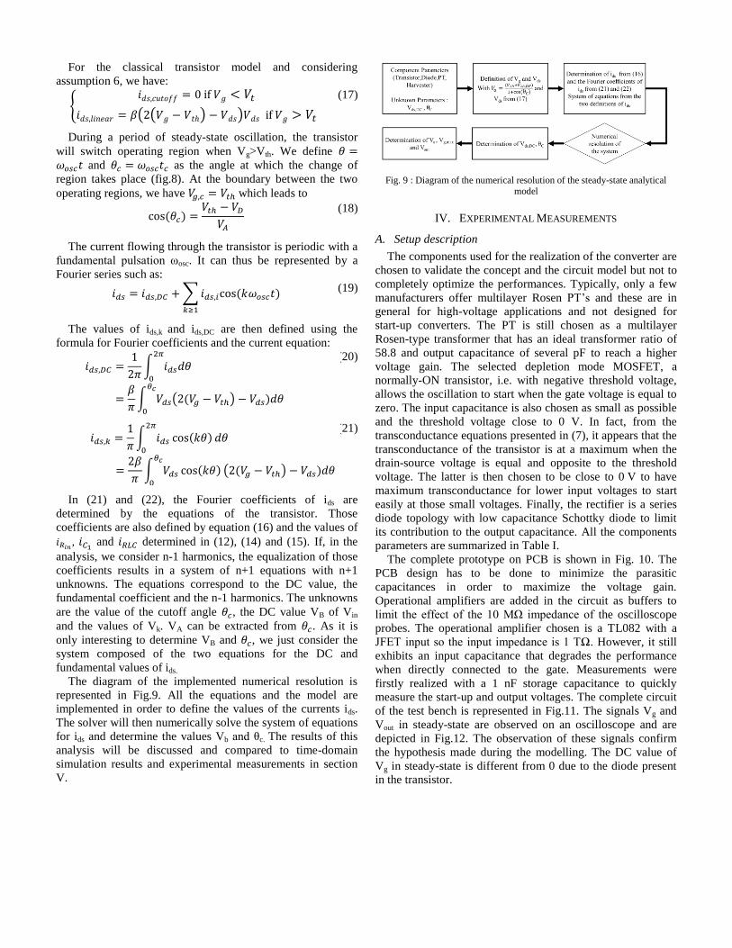
The diagram of the implemented numerical resolution is
represented in Fig.9. All the equations and the model are
implemented in order to define the values of the currents ids.
The solver will then numerically solve the system of equations
for ids and determine the values Vb and θc. The results of this
analysis will be discussed and compared to time-domain
simulation results and experimental measurements in section
V.
Fig. 9 : Diagram of the numerical resolution of the steady-state analytical
model
IV. EXPERIMENTAL MEASUREMENTS
A. Setup description
The components used for the realization of the converter are
chosen to validate the concept and the circuit model but not to
completely optimize the performances. Typically, only a few
manufacturers offer multilayer Rosen PT’s and these are in
general for high-voltage applications and not designed for
start-up converters. The PT is still chosen as a multilayer
Rosen-type transformer that has an ideal transformer ratio of
58.8 and output capacitance of several pF to reach a higher
voltage gain. The selected depletion mode MOSFET, a
normally-ON transistor, i.e. with negative threshold voltage,
allows the oscillation to start when the gate voltage is equal to
zero. The input capacitance is also chosen as small as possible
and the threshold voltage close to 0 V. In fact, from the
transconductance equations presented in (7), it appears that the
transconductance of the transistor is at a maximum when the
drain-source voltage is equal and opposite to the threshold
voltage. The latter is then chosen to be close to 0 V to have
maximum transconductance for lower input voltages to start
easily at those small voltages. Finally, the rectifier is a series
diode topology with low capacitance Schottky diode to limit
its contribution to the output capacitance. All the components
parameters are summarized in Table I.
The complete prototype on PCB is shown in Fig. 10. The
PCB design has to be done to minimize the parasitic
capacitances in order to maximize the voltage gain.
Operational amplifiers are added in the circuit as buffers to
limit the effect of the 10 MΩ impedance of the oscilloscope
probes. The operational amplifier chosen is a TL082 with a
JFET input so the input impedance is 1 TΩ. However, it still
exhibits an input capacitance that degrades the performance
when directly connected to the gate. Measurements were
firstly realized with a 1 nF storage capacitance to quickly
measure the start-up and output voltages. The complete circuit
of the test bench is represented in Fig.11. The signals Vg and
Vout in steady-state are observed on an oscilloscope and are
depicted in Fig.12. The observation of these signals confirm
the hypothesis made during the modelling. The DC value of
Vg in steady-state is different from 0 due to the diode present
in the transistor.
Fig. 10: PCB of the proposed start-up converter.
Fig. 11: Circuit of the experimental test bench
Finally, the measurements are realized with a thermo-
electric generator whose harvester internal resistance is of 2.8
Ω. The Seebeck coefficient of the TEG is of 6 mV/K. A
temperature gradient is applied to the TEG and thus a voltage
appears at the output of the harvester. The change in the
gradient of temperature will change proportionally the value
of this voltage Vin. The harvester output is then connected to
the input of the start-up converter. If the temperature gradient
applied is smaller than 17 K then the voltage at the input of the
converter will be lower than 100 mV confirming the necessity
for a start-up converter.
Fig. 12 : Signal waveforms of Vout and Vg in steady-state
B. Measurements
In a first step, the step-up performances and the sensitivity
to Rin values have been characterized with a TEG. The TEG is
placed between two metal plates: one is in contact with a heat-
sink and the other one with a transistor that increases the
temperature. The voltage generated by the TEG Vin is
monitored at the input of the converter. Fig. 13 shows the
output voltage for different biasing resistances Rin as a
function of the input voltage Vin. For a biasing resistance of
390 Ω, the output voltage reaches 1 V for input voltages as
low as 43 mV. In this configuration, the oscillation starts for
an input voltage of 25 mV and the output reaches 400 mV. On
the other hand, in the case of a 2200 Ω biasing resistance,
oscillation will start when Vin is equal to 15 mV but will only
reach 1 V at an input voltage of 82 mV. For input voltages
higher than 50 mV, the value of the biasing resistance is
directly related to the output voltage value: when the biasing
resistance gets smaller, the circuit presents a higher voltage
gain. At smaller input voltages the influence of the biasing
resistance Rin on the output voltage is not as clear. Indeed, in a
configuration with smaller biasing resistance, the oscillation
may not start at ultra-low voltages. For example, at 30 mV, the
circuit with a biasing resistance of 680 Ω presents a higher
voltage gain than the ones with Rin = 390 Ω and Rin = 2200 Ω.
Fig. 13: Measured voltage gain as a function of Vin for different values of Rin
In this part we have been interested in characterizing the
minimum values of Vin leading to start the oscillation. Fig. 14
shows the minimum input voltage at which we begin to see a
charging of a capacitance as a function of Rin. The gain of the
converter Vout
Vin at the start-up voltage is also presented. The
start-up voltage can be as low as 15 mV for a biasing
resistance of 2 kΩ. At a lower resistance, the circuit starts at
higher input voltages. Here, we also observe an optimum
value for the biasing resistance that minimizes the start-up
voltage. On the other hand, even though oscillations start at
this voltage, the gain is only equal to 2 leading to a very low
output voltage which fails to start the main converter shown in
Fig. 1. The output voltage at start-up will generally be lower
as the biasing resistance increases. As the open-loop gain GOL
will grow with Rin by equation (9), when the biasing resistance
is small, GOL will be smaller and the oscillation won’t start at
low voltages due to the Barkhausen criterion. On the other
hand, if the resistance becomes too large, the drain-source
voltage of the transistor decreases and so the transconductance
decreases as seen in (7) leading to a decrease in the open-loop
gain GOL. Finally, those two behaviors lead to an optimum
value for Rin that minimizes the start-up voltage.
Fig. 14: Measured minimum start-up voltage and gain Vout/Vin of the converter
at the start-up voltage for different biasing resistances
Finally, the start-up performances can be summarized in
Table II. Herein are represented the start-up voltages and the
minimum values of the input voltage to reach an output
voltage of 1 V. Indeed, the function of the circuit is to charge a
storage capacitor at a certain voltage in order to start the main
DC-DC converter. Thus, an important parameter in the design
is to obtain the minimum input voltage at which the output
will reach this threshold voltage that will start the main
converter. In this case, we choose arbitrary a value of 1 V for
the threshold voltage. The minimum values for each parameter
are in bold. The optimum biasing resistance values for the
start-up and voltage gain are different. Moreover, the
minimum value of Vin to reach Vout = 1 V is dependent on the
start-up voltage. For a biasing resistance of 220 Ω, the circuit
only starts at 68 mV and at this voltage, Vout= 1.75 V whereas
with Rin = 270 Ω, the circuit starts at lower voltages and can
reach an output voltage of 1 V at Vin = 43 mV. In the end, the
choice of the biasing resistance value will depend on the
voltage across Cstart needed to start the optimized converter.
V. DISCUSSION
A. Model validation
The experimental realization presented in the previous
section validates the behavior of the start-up converter. In
order to validate the models, we will compare the results
obtained with the analytical modeling, the electrical
simulations based on components models given by the
manufacturers and the experimental measurements. The time-
domain simulations were realized with LTSpice where the
circuit presented in Fig. 4 was used. All the values used for the
simulation are the ones presented in Table I. The models of
the transistor and the diode were given directly by the
manufacturer. The analytical modeling was implemented in
Matlab as presented in III.
The results of the start-up phase analysis were not
considered in terms of start-up voltage as the Barkhausen
criterion classically used in the analysis is only necessary but
insufficient in determining the start of the oscillation. In fact,
the minimum start-up voltages determined numerically were
much lower than the ones measured. The start-up phase
analysis is still useful in order to have a better understanding
of the behavior of the converter and the trade-off of the
different parameters in the start-up.
In steady state, the maximum output voltage was extracted
directly from the LTSpice simulation and compared to the
Matlab analytical results and experiments. Fig. 15 presents the
comparison of the three different approaches (analytical/Spice
simulations/measurements) for biasing resistances of 270 Ω
and 1000 Ω.
Fig. 15: Comparison of the output voltage given by the analytical model,
simulation and measurements
As can be seen from Fig. 15, the results of the numerical
analysis, simulation and measurements are similar and follow
the same behavior. However, there are differences in absolute
value between the three results. For the two Rin values, the
simulation tends to give lower output voltage than the
measurements. For the analytical model, it depends on the
biasing resistance value Rin but in the range from 40 to 70 mV
it fits quite well the experimental results. The errors between
the analytical model results and measurements are 5.8 % and
8.3 % for respectively the cases Rin = 270 Ω and Rin = 1000 Ω.
Between the simulation and measurements the errors are
respectively 8.3 % and 10 %. The differences in the values
have several origins. The minimum value of Vg defined by the
transistor diode threshold voltage changes as a function of the
input voltage in the simulation and experimentation but
assumed as constant in the analytical model.
TABLE II
MEASUREMENT RESULTS
Rin (Ω) 220 270 330 390 470 560 680 820 1000 1200 1500 1800 2200 2700 3300
Start-up voltage
(mV) 68 42,4 34,4 29,4 25 22,8 20 18,6 17,5 16,5 15,8 15 15 15,2 15,7
Vin (mV) to obtain
Vout = 1V 68 43 44 45 46 47,5 49 53 57 61 68 73 82 95 107
This leads to a different DC value for the gate voltage. The
drain-source capacitance is not considered. In addition, the
analysis was realized considering a four-point electrode PT
whereas a three-point one is used in the simulation and
experimental realization. The parameters used in the analytical
model and the LTSpice simulations were determined
experimentally. More specifically, the parameters of the PT
come from impedance measurements and may not reflect the
real parameters of the PT and the load capacitance was
estimated from the capacitance of the copper tracks and the
different parasitic capacitance that influence the value of Cout.
Finally, errors also come from the measurements themselves.
B. Influence of the harvester internal resistance
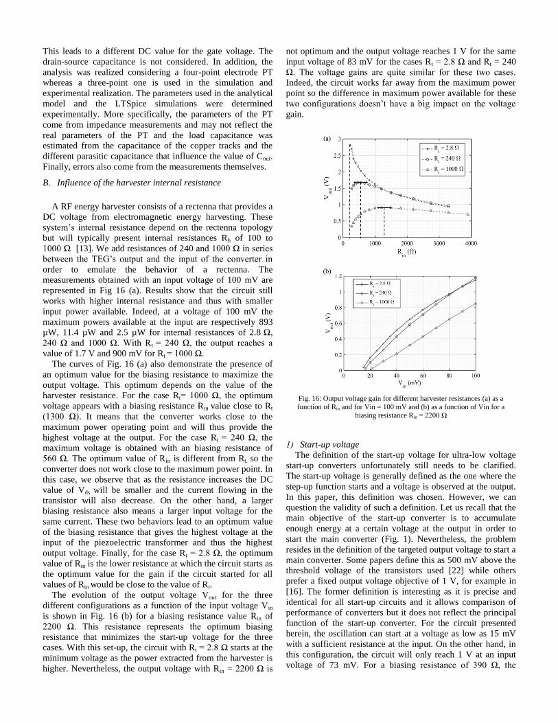
A RF energy harvester consists of a rectenna that provides a
DC voltage from electromagnetic energy harvesting. These
system’s internal resistance depend on the rectenna topology
but will typically present internal resistances Rh of 100 to
1000 Ω [13]. We add resistances of 240 and 1000 Ω in series
between the TEG’s output and the input of the converter in
order to emulate the behavior of a rectenna. The
measurements obtained with an input voltage of 100 mV are
represented in Fig 16 (a). Results show that the circuit still
works with higher internal resistance and thus with smaller
input power available. Indeed, at a voltage of 100 mV the
maximum powers available at the input are respectively 893
µW, 11.4 µW and 2.5 µW for internal resistances of 2.8 Ω,
240 Ω and 1000 Ω. With Rt = 240 Ω, the output reaches a
value of 1.7 V and 900 mV for Rt = 1000 Ω.
The curves of Fig. 16 (a) also demonstrate the presence of
an optimum value for the biasing resistance to maximize the
output voltage. This optimum depends on the value of the
harvester resistance. For the case Rt= 1000 Ω, the optimum
voltage appears with a biasing resistance Rin value close to Rt
(1300 Ω). It means that the converter works close to the
maximum power operating point and will thus provide the
highest voltage at the output. For the case Rt = 240 Ω, the
maximum voltage is obtained with an biasing resistance of
560 Ω. The optimum value of Rin is different from Rt. so the
converter does not work close to the maximum power point. In
this case, we observe that as the resistance increases the DC
value of Vds will be smaller and the current flowing in the
transistor will also decrease. On the other hand, a larger
biasing resistance also means a larger input voltage for the
same current. These two behaviors lead to an optimum value
of the biasing resistance that gives the highest voltage at the
input of the piezoelectric transformer and thus the highest
output voltage. Finally, for the case Rt = 2.8 Ω, the optimum
value of Rin is the lower resistance at which the circuit starts as
the optimum value for the gain if the circuit started for all
values of Rin would be close to the value of Rt.
The evolution of the output voltage Vout for the three
different configurations as a function of the input voltage Vin
is shown in Fig. 16 (b) for a biasing resistance value Rin of
2200 Ω. This resistance represents the optimum biasing
resistance that minimizes the start-up voltage for the three
cases. With this set-up, the circuit with Rt = 2.8 Ω starts at the
minimum voltage as the power extracted from the harvester is
higher. Nevertheless, the output voltage with Rin = 2200 Ω is
not optimum and the output voltage reaches 1 V for the same
input voltage of 83 mV for the cases Rt = 2.8 Ω and Rt = 240
Ω. The voltage gains are quite similar for these two cases.
Indeed, the circuit works far away from the maximum power
point so the difference in maximum power available for these
two configurations doesn’t have a big impact on the voltage
gain.
Fig. 16: Output voltage gain for different harvester resistances (a) as a
function of Rin and for Vin = 100 mV and (b) as a function of Vin for a
biasing resistance Rin = 2200 Ω
1) Start-up voltage
The definition of the start-up voltage for ultra-low voltage
start-up converters unfortunately still needs to be clarified.
The start-up voltage is generally defined as the one where the
step-up function starts and a voltage is observed at the output.
In this paper, this definition was chosen. However, we can
question the validity of such a definition. Let us recall that the
main objective of the start-up converter is to accumulate
enough energy at a certain voltage at the output in order to
start the main converter (Fig. 1). Nevertheless, the problem
resides in the definition of the targeted output voltage to start a
main converter. Some papers define this as 500 mV above the
threshold voltage of the transistors used [22] while others
prefer a fixed output voltage objective of 1 V, for example in
[16]. The former definition is interesting as it is precise and
identical for all start-up circuits and it allows comparison of
performance of converters but it does not reflect the principal
function of the start-up converter. For the circuit presented
herein, the oscillation can start at a voltage as low as 15 mV
with a sufficient resistance at the input. On the other hand, in
this configuration, the circuit will only reach 1 V at an input
voltage of 73 mV. For a biasing resistance of 390 Ω, the
circuit will start at only 29.4 mV but reaches 1 V with an input
voltage of only 45 mV.
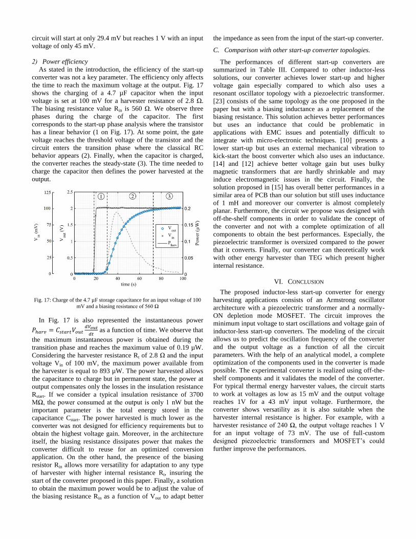
2) Power efficiency
As stated in the introduction, the efficiency of the start-up
converter was not a key parameter. The efficiency only affects
the time to reach the maximum voltage at the output. Fig. 17
shows the charging of a 4.7 µF capacitor when the input
voltage is set at 100 mV for a harvester resistance of 2.8 Ω.
The biasing resistance value Rin is 560 Ω. We observe three
phases during the charge of the capacitor. The first
corresponds to the start-up phase analysis where the transistor
has a linear behavior (1 on Fig. 17). At some point, the gate
voltage reaches the threshold voltage of the transistor and the
circuit enters the transition phase where the classical RC
behavior appears (2). Finally, when the capacitor is charged,
the converter reaches the steady-state (3). The time needed to
charge the capacitor then defines the power harvested at the
output.
Fig. 17: Charge of the 4.7 µF storage capacitance for an input voltage of 100
mV and a biasing resistance of 560 Ω
In Fig. 17 is also represented the instantaneous power
𝑃ℎ𝑎𝑟𝑣 = 𝐶𝑠𝑡𝑎𝑟𝑡𝑉𝑜𝑢𝑡𝑑𝑉𝑜𝑢𝑡
𝑑𝑡 as a function of time. We observe that
the maximum instantaneous power is obtained during the
transition phase and reaches the maximum value of 0.19 µW.
Considering the harvester resistance Rt of 2.8 Ω and the input
voltage Vin of 100 mV, the maximum power available from
the harvester is equal to 893 µW. The power harvested allows
the capacitance to charge but in permanent state, the power at
output compensates only the losses in the insulation resistance
Rstart. If we consider a typical insulation resistance of 3700
MΩ, the power consumed at the output is only 1 nW but the
important parameter is the total energy stored in the
capacitance Cstart. The power harvested is much lower as the
converter was not designed for efficiency requirements but to
obtain the highest voltage gain. Moreover, in the architecture
itself, the biasing resistance dissipates power that makes the
converter difficult to reuse for an optimized conversion
application. On the other hand, the presence of the biasing
resistor Rin allows more versatility for adaptation to any type
of harvester with higher internal resistance Rt, insuring the
start of the converter proposed in this paper. Finally, a solution
to obtain the maximum power would be to adjust the value of
the biasing resistance Rin as a function of Vout to adapt better
the impedance as seen from the input of the start-up converter.
C. Comparison with other start-up converter topologies.
The performances of different start-up converters are
summarized in Table III. Compared to other inductor-less
solutions, our converter achieves lower start-up and higher
voltage gain especially compared to which also uses a
resonant oscillator topology with a piezoelectric transformer.
[23] consists of the same topology as the one proposed in the
paper but with a biasing inductance as a replacement of the
biasing resistance. This solution achieves better performances
but uses an inductance that could be problematic in
applications with EMC issues and potentially difficult to
integrate with micro-electronic techniques. [10] presents a
lower start-up but uses an external mechanical vibration to
kick-start the boost converter which also uses an inductance.
[14] and [12] achieve better voltage gain but uses bulky
magnetic transformers that are hardly shrinkable and may
induce electromagnetic issues in the circuit. Finally, the
solution proposed in [15] has overall better performances in a
similar area of PCB than our solution but still uses inductance
of 1 mH and moreover our converter is almost completely
planar. Furthermore, the circuit we propose was designed with
off-the-shelf components in order to validate the concept of
the converter and not with a complete optimization of all
components to obtain the best performances. Especially, the
piezoelectric transformer is oversized compared to the power
that it converts. Finally, our converter can theoretically work
with other energy harvester than TEG which present higher
internal resistance.
VI. CONCLUSION
The proposed inductor-less start-up converter for energy
harvesting applications consists of an Armstrong oscillator
architecture with a piezoelectric transformer and a normally-
ON depletion mode MOSFET. The circuit improves the
minimum input voltage to start oscillations and voltage gain of
inductor-less start-up converters. The modeling of the circuit
allows us to predict the oscillation frequency of the converter
and the output voltage as a function of all the circuit
parameters. With the help of an analytical model, a complete
optimization of the components used in the converter is made
possible. The experimental converter is realized using off-the-
shelf components and it validates the model of the converter.
For typical thermal energy harvester values, the circuit starts
to work at voltages as low as 15 mV and the output voltage
reaches 1V for a 43 mV input voltage. Furthermore, the
converter shows versatility as it is also suitable when the
harvester internal resistance is higher. For example, with a
harvester resistance of 240 Ω, the output voltage reaches 1 V
for an input voltage of 73 mV. The use of full-custom
designed piezoelectric transformers and MOSFET’s could
further improve the performances.
TABLE III
COMPARISON BETWEEN START-UP CONVERTER TOPOLOGIES
Ref. Converter architecture Particular elements Analytical
Models Minimum start-up
voltage (mV) Minimum Vin to obtain
Vout = 1 V (mV)
[9] Inductor-less Charge pump No No 200 250
[10] Boost Mechanical switch + external
vibration No 35 35
[15] Ultra low voltage oscillator
and charge pump 1 mH inductance
Start-up and
steady-state 10 10
[14] Resonant oscillator 7 magnetic transformers in
series No 6 6
[12] Resonant oscillator Magnetic transformer Start-up 40 40
[22] Resonant oscillator Piezoelectric transformer +
biasing inductance Start-up 32 46
[22] Inductor-less resonant
oscillator Piezoelectric transformer Start-up 69 69
[23] Resonant oscillator Piezoelectric transformer +
inductor Start-up 12 18
This
Work
Inductor-less resonant
oscillator
Piezoelectric transformer +
biasing resistance
Start-up and
steady-state 15 43
REFERENCES
[1] C. Knight, J. Davidson, and S. Behrens, “Energy Options
for Wireless Sensor Nodes,” Sensors, vol. 8, no. 12, pp.
8037–8066, Dec. 2008.
[2] R. J. M. Vullers, R. van Schaijk, I. Doms, C. Van Hoof,
and R. Mertens, “Micropower energy harvesting,” Solid-
State Electron., vol. 53, no. 7, pp. 684–693, Jul. 2009.
[3] S.-E. Adami, “Optimisation de la récupération d’énergie
dans les applications de rectenna.”, Ph. D.
Dissertation Ecole centrale de Lyon, Ecully, France,
2013.
[4] S. Bandyopadhyay and A. P. Chandrakasan, “Platform
Architecture for Solar, Thermal, and Vibration Energy
Combining With MPPT and Single Inductor,” IEEE J.
Solid-State Circuits, vol. 47, no. 9, pp. 2199–2215, Sep.
2012.
[5] A. Richelli, L. Colalongo, S. Tonoli, and Z. M. KovÁcs-
Vajna, “A 0.2 V DC/DC Boost Converter for Power
Harvesting Applications,” IEEE Trans. Power Electron.,
vol. 24, no. 6, pp. 1541–1546, Jun. 2009.
[6] J. Kim and C. Kim, “A DC-DC Boost Converter With
Variation-Tolerant MPPT Technique and Efficient ZCS
Circuit for Thermoelectric Energy Harvesting
Applications,” IEEE Trans. Power Electron., vol. 28, no.
8, pp. 3827–3833, Aug. 2013.
[7] M. Dini, A. Romani, M. Filippi, and M. Tartagni, “A
Nanocurrent Power Management IC for Low-Voltage
Energy Harvesting Sources,” IEEE Trans. Power
Electron., vol. 31, no. 6, pp. 4292–4304, Jun. 2016.
[8] P.-H. Chen et al., “0.18-V input charge pump with
forward body biasing in startup circuit using 65nm
CMOS,” in 2010 IEEE Custom Integrated Circuits
Conference (CICC), 2010, pp. 1–4.
[9] G. Pillonnet and T. Martinez, “Sub-threshold startup
charge pump using depletion MOSFET for a low-voltage
harvesting application,” in 2015 IEEE Energy Conversion
Congress and Exposition (ECCE), 2015, pp. 3143–3147.
[10] Y. K. Ramadass and A. P. Chandrakasan, “A Battery-
Less Thermoelectric Energy Harvesting Interface Circuit
With 35 mV Startup Voltage,” IEEE J. Solid-State
Circuits, vol. 46, no. 1, pp. 333–341, Jan. 2011.
[11] E. H. Armstrong, “Wireless receiving system.,” US
1113149 A, 06-Oct-1914.
[12] J. P. Im et al., “A 40mV transformer-reuse self-startup
boost converter with MPPT control for thermoelectric
energy harvesting,” in 2012 IEEE International Solid-
State Circuits Conference, 2012, pp. 104–106.
[13] S.-E. Adami et al., “Ultra-Low Power, Low Voltage,
Self-Powered Resonant DC-DC Converter for Energy
Harvesting,” J. Low Power Electron., vol. 9, no. 1, pp.
103–117, Apr. 2013.
[14] D. Grgić, T. Ungan, M. Kostić, and L. M. Reindl, “Ultra-
low input voltage DC-DC converter for micro energy
harvesting,” in PowerMeMs, 2009, pp. 265–268.
[15] M. B. Machado, M. Sawan, M. C. Schneider, and C.
Galup-Montoro, “10 mV - 1V step-up converter for
energy harvesting applications,” in 27th Symposium on
Integrated Circuits and Systems Design (SBCCI), 2014,
pp. 1–5.
[16] G. Bassi, L. Colalongo, A. Richelli, and Z. M. Kovacs-
Vajna, “100 mV-1.2 V fully-integrated DC -DC
converters for thermal energy harvesting,” IET Power
Electron., vol. 6, no. 6, pp. 1151–1156, Jul. 2013.
[17] E. Wells, “Comparing magnetic and piezoelectric
transformer approaches in CCFL applications,” Analog
Appl J, no. Q1, pp. 12–17, 2002.
[18] S. S. Bedair, J. S. Pulskamp, R. G. Polcawich, B.
Morgan, J. L. Martin, and B. Power, “Thin-Film
Piezoelectric-on-Silicon Resonant Transformers,” J.
Microelectromechanical Syst., vol. 22, no. 6, pp. 1383–
1394, Dec. 2013.
[19] D. Vasic, F. Costa, and E. Sarraute, “Comparing
piezoelectric and coreless electromagnetic transformer
approaches in IGBT driver,” Eur. Phys. J. - Appl. Phys.,
vol. 34, no. 3, pp. 237–242, 2006.
[20] M. W. Hooker, “Properties of PZT-based piezoelectric
ceramics between-150 and 250 °C,” Technical report
NASA/CR-208708, 1998.
[21] D. Vasic, “Apports des matériaux piézoélectriques pour
l’intégration hybride et monolithique des
transformateurs.” Ph.D. Dissertation, Ecole normale
supérieure, Cachan, France, 2003.
[22] A. Camarda, A. Romani, E. Macrelli, and M. Tartagni,
“A 32 mV/69 mV input voltage booster based on a
piezoelectric transformer for energy harvesting
applications,” Sens. Actuators Phys., vol. 232, pp. 341–
352, Aug. 2015.
[23] T. Martinez, G. Pillonnet, and F. Costa, “A 12 mV start-
up converter using piezoelectric transformer for energy
harvesting applications,” J. Phys. Conf. Ser., vol. 773, no.
1, p. 12028, 2016.
[24] E. M. Syed, F. P. Dawson, and E. S. Rogers, “Analysis
and modeling of a Rosen type piezoelectric transformer,”
in Power Electronics Specialists Conference, 2001.
PESC. 2001 IEEE 32nd Annual, 2001, vol. 4, pp. 1761–
1766.
[25] W. Zhiming, Y. Xinghong, and J. Y. X. Guangzhong,
“The analysis of multilayer piezoelectric transformer,” in
2005 12th International Symposium on Electrets, 2005,
pp. 165–167.
[26] “Multi Layer Piezo Transformer Step Up Ratio 45 -
SMMTF53P3S45- STEMINC.” [Online]. Available:
https://www.steminc.com/PZT/en/piezo-transformer-55-
khz-3w. [Accessed: 23-May-2016].
[27] “ALD210800 - ALD210800.pdf.” [Online]. Available:
http://www.aldinc.com/pdf/ALD210800.pdf..
[28] K. Mayaram, “Output voltage analysis for the MOS
Colpitts oscillator,” IEEE Trans. Circuits Syst. Fundam.
Theory Appl., vol. 47, no. 2, pp. 260–263, Feb. 2000.
T. Martinez was born in Montluçon, France in 1992. He
received an Engineering degree in Electrical Engineering from
Ecole Polytechnique in 2015 and a M. Sc degree in Micro and
Nano Electronics from the Ecole Polytechnique Federale de
Lausanne in 2016. He joined the SATIE laboratory for his
Master Thesis in 2015 where he is currently working on his
Ph. D. thesis. His current research interest include low power
electronics for energy harvesting and piezoelectric devices for
energy conversion.
G. Pillonnet was born in Lyon, France,
in 1981. He received his Master degree in
Electrical Engineering from CPE Lyon,
France in 2004, a PhD and habilitation
degrees from INSA Lyon, France in 2007
and 2016 respectively. Following an early
experience as analog designer in
STMicroelectronics in 2008, he joined
University of Lyon in the Electrical
Engineering department. During the 2011-12 academic year,
he held a visiting researcher position at the University of
California at Berkeley. Since 2013, he has worked as full-time
researcher at the CEA-LETI, a major French research
institution. His research focuses on low power electronics
using heterogeneous devices including modeling, circuit
design and control techniques. He has published more than 70
papers in his areas of interest.
F. Costa received the Ph.D. in electrical
engineering, entitled "EMI in HF power
electronics" from the University of
Paris-Sud, Orsay, France, in 1992 and
the "Habilitation à diriger des
recherches (HDR)" in 1998 from the
university Paris-Sud Orsay. After
being assistant professor from 1994 to
2003 in Ecole Normale Supérieure de
Cachan (ENSC), he is a Full Professor
in University Paris Est Créteil (UPEC),
France since 2003, where he is responsible for the master
degree in education in sciences & technology in the "Ecole
Supérieure de l'Education et du Professorat (ESPE)". Since
2013, he is responsible for the "components & systems for
electrical energy" department (CSEE) of lab SATIE CNRS.
This department covers all the fields of research in electrical
power conversion: design & integration in power electronics,
reliability of power components, EMI issues, materials for
electrical energy, electrical actuators design and control. His
research fields include high-frequency medium-power
converters, EMI issues and modelling, HF instrumentation,
integration in power electronics, piezoelectric converters and
low-level energy harvesting systems. He is the author or co-
author of more than 60 journal papers, 3 books and more than
150 conference papers.