Embed Size (px)
Citation preview

*Other brands and names are the property of their respective owners.Information in this document is provided in connection with Intel products. Intel assumes no liability whatsoever, including infringement of any patent orcopyright, for sale and use of Intel products except as provided in Intel’s Terms and Conditions of Sale for such products. Intel retains the right to makechanges to these specifications at any time, without notice. Microcomputer Products may have minor variations to this specification known as errata.
November 1994COPYRIGHT © INTEL CORPORATION, 1995 Order Number: 272337-002
8XC51GBCHMOS SINGLE-CHIP 8-BIT MICROCONTROLLER
Commercial/Express
87C51GBÐ8 Kbytes OTP/8 Kbytes Internal Program Memory
83C51GBÐ8 Kbytes Factory Programmable ROM
80C51GBÐCPU with RAM and I/O
8XC51GBÐ3.5 MHz to 12 MHz g20% VCC
8XC51GB-1Ð3.5 MHz to 16 MHz g20% VCC
Y 8 Kbytes On-Chip ROM/OTP ROM
Y 256 Bytes of On-Chip Data RAM
Y Two Programmable Counter Arrayswith:Ð 2 x 5 High Speed Input/Output
Channels Compare/CaptureÐ Pulse Width ModulatorsÐ Watchdog Timer Capabilities
Y Three 16-Bit Timer/Counters withÐ Four Programmable Modes:Ð Capture, Baud Rate Generation
(Timer 2)
Y Dedicated Watchdog Timer
Y 8-Bit, 8-Channel A/D with:Ð Eight 8-Bit Result RegistersÐ Four Programmable Modes
Y Programmable Serial Channel with:Ð Framing Error DetectionÐ Automatic Address Recognition
Y Serial Expansion Port
Y Programmable Clock Out
Y Extended Temperature Range:(b40§C to a85§C)
Y 48 Programmable I/O Lines with40 Schmitt Trigger Inputs
Y 15 Interrupt Sources with:Ð 7 External, 8 Internal SourcesÐ 4 Programmable Priority Levels
Y Pre-Determined Port States on Reset
Y High Performance CHMOS Process
Y TTL and CHMOS Compatible LogicLevels
Y Power Saving Modes
Y 64K External Data Memory Space
Y 64K External Program Memory Space
Y Three Level Program Lock System
Y ONCE (ON-Circuit Emulation) Mode
Y Quick Pulse Programming Algorithm
Y MCSÉ 51 Microcontroller FullyCompatible Instruction Set
Y Boolean Processor
Y Oscillator Fail Detect
Y Available in 68-Pin PLCC
MEMORY ORGANIZATION
PROGRAM MEMORY: Up to 8 Kbytes of the program memory can reside in the on-chip ROM. Also, the devicecan address up to 64K of program memory external to the chip.
DATA MEMORY: This microcontroller has a 256 x 8 on-chip RAM. In addition it can address up to 64 Kbytes ofexternal data memory.
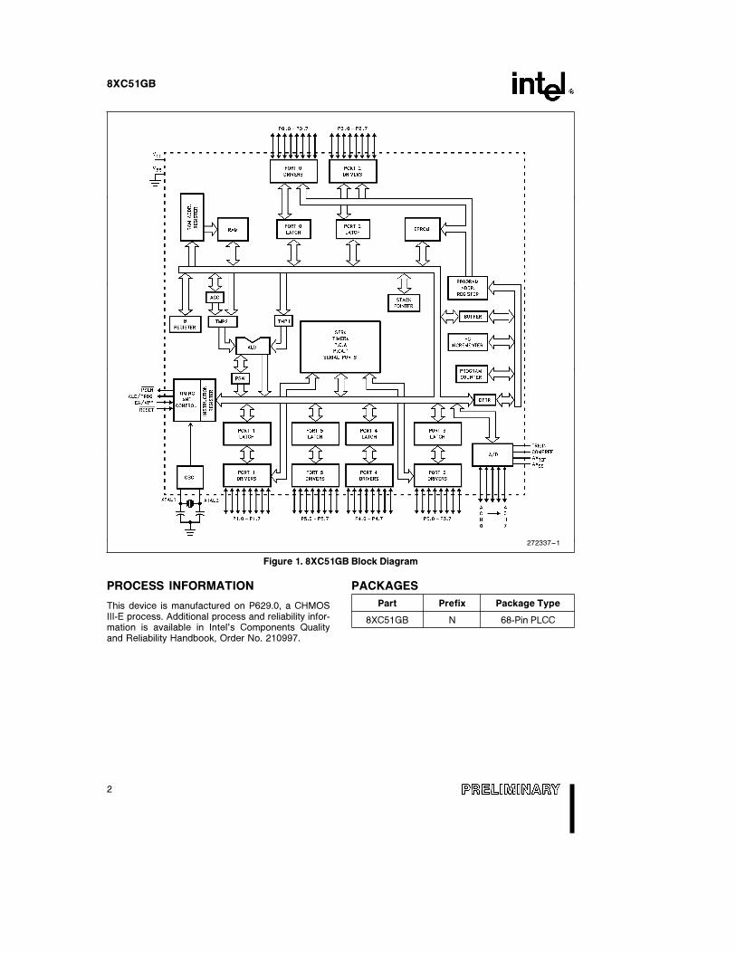
The Intel 8XC51GB is a single-chip control oriented microcontroller which is fabricated on Intel’s CHMOS III-Etechnology. The 8XC51GB is an enhanced version of the 8XC51FA and uses the same powerful instructionset and architecture as existing MCS 51 microcontroller products. Added features make it an even morepowerful microcontroller for applications that require On-Chip A/D, Pulse Width Modulation, High Speed I/O,up/down counting capabilities and memory protection features. It also has a more versatile serial channel thatfacilitates multi-processor communications.
8XC51GB
272337–1
Figure 1. 8XC51GB Block Diagram
PROCESS INFORMATION
This device is manufactured on P629.0, a CHMOSIII-E process. Additional process and reliability infor-mation is available in Intel’s Components Qualityand Reliability Handbook, Order No. 210997.
PACKAGES
Part Prefix Package Type
8XC51GB N 68-Pin PLCC
2

8XC51GB
PARALLEL I/O PORTS
The 8XC51GB contains six 8-bit parallel I/O ports.All six ports are bidirectional and consist of a latch,an output driver, and an input buffer. Many of theport pins have multiplexed I/O and control functions.
Port Pins as Outputs
Port 0 has open drain outputs when it is not servingas the external data bus. The internal pullup is activeonly when the pin is outputting a logic 1 during exter-nal memory access. An external pullup resistor isrequired on Port 0 when it is serving as an outputport.
Ports 1, 2, 3, 4, and 5 have quasi-bidirectional out-puts. A strong pullup provides a fast rise time whenthe pin is set to a logic 1. This pullup turns on for twooscillator periods to drive the pin high and then turnsoff. The pin is held high by a weak pullup.
Writing the P0, P1, P2, P3, P4 or P5 Special FunctionRegister sets the corresponding port pins. All sixport registers are bit addressable.
Port Pins as Inputs
The pins of all six ports are configured as inputs bywriting a logic 1 to them. Since Port 0 is an opendrain port, it provides a very high input impedance.Since pins of Port 1, 2, 3, 4 and 5 have weak pullups(which are always on), they source a small currentwhen driven low externally. All ports except Port 0have Schmitt trigger inputs.
Port States During Reset
Ports 0 and 3 reset asynchronously to a one andPorts 1, 2, 4, and 5 reset to a zero asynchronously.
PIN DESCRIPTIONS
The 8XC51GB will be packaged in the 68-lead PLCCpackage. Its pin assignment is shown in Figure 2.
VCC: Supply Voltage.
VSS: Circuit Ground.
Diagram is for Pin Reference Only. Package Size is Not to Scale.
272337–2*OTP only
Figure 2. Pin Connections
3

8XC51GB
ALTERNATE PORT FUNCTIONSPorts 0, 1, 2, 3, 4 and 5 have alternate functions as well as their I/O function as described below.
Port Pin Alternate Function
P0.0/ADO–P0.7/AD7 Multiplexed Address/Data for External Memory
P1.0/T2 Timer 2 External Clock Input/Clock-Out
P1.1/T2EX Timer 2 Reload/Capture/Direction Control
P1.2/ECI PCA External Clock Input
P1.3/CEXO–P1.7/CEX4 PCA Capture Input, Compare/PWM Output
P2.0/A8–P2.7/A15 High Byte of Address for External Memory
P3.0/RXD Serial Port Input
P3.1/TXD Serial Port Output
P3.2/INT0 External Interrupt 0
P3.3/INT1 External Interrupt 1
P3.4/T0 Timer 0 External Clock Input
P3.5/T1 Timer 1 External Clock Input
P3.6/WR Write Strobe for External Memory
P3.7/RD Read Strobe for External Memory
P4.0/SEPCLK Clock Source for Serial Expansion Port
P4.1/SEPDAT Data I/O for the Serial Expansion Port
P4.2/ECI1 PCA1 External Clock Input
P4.3/C1EX0–P4.7/C1EX4 PCA1 Capture Input, Compare/PWM Output
P5.2/INT2–P5.6/INT6 External Interrupt INT2–INT6
RST: Reset input. A low on this pin for two machinecycles while the oscillator is running resets the de-vice. The port pins will be driven to their reset condi-tion when a voltage below VIL max voltage is ap-plied, whether the oscillator is running or not. Aninternal pullup resistor permits a power-on reset withonly a capacitor connected to VSS.
ALE/PROG: Address Latch Enable output pulse forlatching the low byte of the address during accessesto external memory. This pin (ALE/PROG) is alsothe program pulse input during programming of the87C51GB.
In normal operation ALE is emitted at a constantrate of (/6 the oscillator frequency, and may be usedfor external timing or clocking purposes. Note, how-ever, that one ALE pulse is skipped during each ac-cess to external Data Memory.
If desired, ALE operation can be disabled by settingbit 0 of SFR location 8EH. With this bit set, the pin isweakly pulled high. However, the ALE disable fea-ture will be suspended during a MOVX or MOVC in-struction, idle mode, power down mode and ICEmode. The ALE disable feature will be terminated byreset. When the ALE disable feature is suspended or
terminated, the ALE pin will no longer be pulled upweakly. Setting the ALE-disable bit has no affect ifthe microcontroller is in external execution mode.
Throughout the remainder of this data sheet, ALEwill refer to the signal coming out of the ALE/PROGpin, and the pin will be referred to as the ALE/PROGpin.
PSEN: Program Store Enable is the read strobe toexternal Program Memory.
When the 8XC51GB is executing code from externalProgram Memory, PSEN is activated twice each ma-chine cycle, except that two PSEN activations areskipped during each access to external Data Memo-ry.
EA/VPP: External Access enable. EA must bestrapped to VSS in order to enable the device tofetch code from external Program Memory locations0000H to 1FFFH. Note, however, that if either of theProgram Lock bits are programmed, EA will be inter-nally latched on reset.
EA should be strapped to VCC for internal programexecutions.
4

8XC51GB
This pin also receives the 12.75V programming sup-ply voltage (VPP) during programming (OTP only).
XTAL1: Input to the inverting oscillator amplifier.
XTAL2: Output from the inverting oscillator amplifi-er.
A/D CONVERTER
The 8XC51GB A/D converter has a resolution of 8bits and an accuracy of g1 LSB (g2 LSB for chan-nels 0 and 1). The conversion time for a single chan-nel is 20 ms at a clock frequency of 16 MHz with thesample and hold function included. Independentsupply voltages are provided for the A/D. Also, theA/D operates both in Normal Mode or in Idle Mode.
The A/D has 8 analog input pins; ACH0 (A/D CHan-nel 0) . . . ACH7, 1 reference input pin; COMPREF(COMParison REFerence), 1 control input pin; TRI-GIN (TRIGger IN), and 2 power pins; AVREF (Volt-age REFerence) and analog ground (ANalogGrouND). In addition, the A/D has 8 conversion re-sult registers; ADRES0 (A/D result for channel 0) . . .ADRES7, 1 comparison result register; ACMP (Ana-log Comparison), and 1 control register; ACON (A/DControl).
The control bit ACE (A/D Conversion Enable) inACON controls whether the A/D is in operation ornot. ACE e 0 idles the A/D. ACE e 1 enables A/Dconversion. The control bit AIM (A/D Input mode) inACON controls the mode of channel selection. AIMe 0 is the Scan Mode, and AIM e 1 is the SelectMode. The result registers ADRES4 . . . ADRES7 al-ways contain the result of a conversion from the cor-responding channels ACH4 . . . CH7. However, theresult registers ADRES0 . . . ADRES3 depend on themode selected. In the scan mode, ADRES0 . . . AD-RES3 contain the values from ACH0 . . . ACH3. Inthe Select Mode, one of the four channels ACH0 . . .ACH3 is converted four times, and the four valuesare stored sequentially in locations ADRES0 . . . AD-RES3. Its channel is selected by bits ACS1 andACS0 (A/D Channel Select 1 and 0) in ACON.
PROGRAMMABLE COUNTER ARRAYS
The Programmable Counter Arrays (PCA–PCA1) areeach made up of a Counter Module and five Regis-ter/Comparator Modules as shown below. The16-bit output of the counter module is available to allfive Register/Comparator Modules, providing one
common timing reference. Each Register/Compara-tor Module is associated with a pin of Port 1 or Port 4and is capable of performing input capture, outputcompare and pulse width modulation functions. ThePCAs are exactly the same in function except for theaddition of clock input sources on PCA1.
The PCA Counter and five Register/ComparatorModules each have a status bit in the CCON/C1CON Special Function Registers. These sixstatus bits are set according to the selected modesof operation described below. The CCON/C1CONRegister provides a convenient means to determinewhich of the six PCA/PCA1 interrupts has occurred.The EC Bit in the IE (Interrupt Enable) Special Func-tion Register is a global interrupt enable for the PCA.
272337–3
Figure 3. Programmable Counter Arrays
OSCILLATOR CHARACTERISTICS
XTAL1 and XTAL2 are the input and output, respec-tively, of an inverting amplifier which can be config-ured for use as an on-chip oscillator, as shown inFigure 4. Either a quartz crystal or ceramic resonatormay be used. More detailed information concerningthe use of the on-chip oscillator is available in Appli-cation Note AP-155, ‘‘Oscillators for Microcontrol-lers,’’ Order No. 230659.
To drive the device from an external clock source,XTAL should be driven, while XTAL2 floats, asshown in Figure 5. There are no requirements on theduty cycle of the external clock signal, since the in-put to the internal clocking circuitry is through a di-vide-by-two flip-flop, but minimum and maximumhigh and low times specified on the data sheet mustbe observed.
5

8XC51GB
272337–4
C1, C2 e 30 pF g10 pF for CrystalsFor Ceramic Resonators contact resonatormanufacturer.
Figure 4. Oscillator Connections
272337–5
Figure 5. External Clock Drive Configuration
IDLE MODE
The user’s software can invoke the Idle Mode. Whenthe microcontroller is in this mode, power consump-tion is reduced. The Special Function Registers andthe onboard RAM retain their values during idle, pe-ripherals continue to operate, but the processorstops executing instructions. Idle Mode will be exitedif the chip is reset or if an enabled interrupt occurs.The PCA timer/counter can optionally be left run-ning or paused during Idle Mode. The WatchdogTimer continues to count in Idle Mode and must beserviced to prevent a device RESET while in Idle.
POWER DOWN MODE
To save even more power, a Power Down mode canbe invoked by software. In this mode, the oscillatoris stopped and the instruction that invoked PowerDown is the last instruction executed. The on-chipRAM and Special Function Registers retain their val-ues until the Power Down mode is terminated.
On the 8XC51GB either a hardware reset or an ex-ternal interrupt can cause an exit from Power Down.Reset redefines all the SFRs but does not changethe on-chip RAM. An external interrupt does not re-define the SFR’s or change the on-chip RAM. Anexternal interrupt will modify the interrupt associatedSFR’s in the same way an interrupt will in all othermodes. The interrupt must be enabled and config-ured as level sensitive. To properly terminate PowerDown the reset or external interrupt should not beexecuted before VCC is restored to its normal oper-ating level. The reset or external interrupt must beheld active long enough for the oscillator to restartand stabilize. The Oscillator Fail Detect must be dis-abled prior to entering Power Down.
DESIGN CONSIDERATIONS
# When the idle mode is terminated by a hardwarereset, the device normally resumes program exe-cution, from where it left off, up to two machinecycles before the internal reset algorithm takescontrol. On-chip hardware inhibits access to inter-nal RAM in this event, but access to the port pinsis not inhibited. To eliminate the possibility of anunexpected write when Idle is terminated by re-set, the instruction following the one that invokesIdle should not be one that writes to a port pin orto external memory.
# As RESET rises, the 8XC51GB will remain in re-set for up to 5 machine cycles (60 oscillator peri-ods) after RESET reaches VIH1.
Table 1. Status of the External Pins during Idle and Power Down
ModeProgram
ALE PSEN PORT0 PORT1 PORT2 PORT3Memory
Idle Internal 1 1 Data Data Data Data
Idle External 1 1 Float Data Address Data
Power Down Internal 0 0 Data Data Data Data
Power Down External 0 0 Float Data Data Data
NOTE:For more detailed information on the reduced power modes refer to current Embedded Microcontrollersand Processors Handbook Volume I (Order No. 270645), and Application Note AP-252 (EmbeddedApplications Handbook, Order No. 270648), ‘‘Designing with the 80C51BH.’’
6

8XC51GB
ONCE MODE
The ONCE (‘‘On-Circuit Emulation’’) Mode facilitatestesting and debugging of systems using the8XC51GB without removing it from the circuit. TheONCE Mode is invoked by:
1) Pulling ALE low while the device is in reset andPSEN is high;
2) Holding ALE low as RESET is deactivated.
While the device is in ONCE Mode, the Port 0 pinsfloat, and the other port pins and ALE and PSEN areweakly pulled high. The oscillator circuit remains ac-tive. While the 8XC51GB is in this mode, an emula-tor or test CPU can be used to drive the circuit. Nor-mal operation is restored when a normal reset is ap-plied.
Watchdog Timer (WDT)
The 8XC51GB contains a dedicated Watchdog Tim-er (WDT) to allow recovery from a software or hard-ware upset. The WDT consists of a 14-bit counterwhich is cleared on Reset, and subsequently incre-mented every machine cycle. While the oscillator isrunning, the WDT will be incrementing and cannotbe disabled. The counter may be reset by writing1EH and E1H in sequence to the WDTRST SpecialFunction Register. If the counter is not reset beforeit reaches 3FFFH (16383D), the chip will be forcedinto a reset sequence by the WDT. This works out to12.28 ms @ 16 MHz. WDTRST is a write only regis-ter. The WDT does not force the external reset pinlow.
While in Idle mode the WDT continues to count. Ifthe user does not wish to exit Idle with a reset, thenthe processor must be periodically ‘‘woken up’’ toservice the WDT. In Power Down mode, the WDTstops counting and holds its current value.
Serial Expansion Port (SEP)
The Serial Expansion Port is a half-duplex synchro-nous serial interface with the following features:
Four Clock FrequenciesÐ XTAL/12, 24, 48, 96.
Four Interface ModesÐ High/Low/Falling/RisingEdges.
Interrupt Driven.
Oscillator Fail Detect (OFD)
The Oscillator Fail Detect circuitry triggers a reset ifthe oscillator frequency is lower than the OFD trig-ger frequency. It can be disabled by software by writ-ing E1H followed by 1EH to the OFDCON register.Before going into Power Down Mode, the OFD mustbe disabled or it will force the GB out of PowerDown. The OFD has the following features.
OFD Trigger Frequency: Below 20 KHz, the8XC51GB will be held in reset. Above 400 KHz,the 8XC51GB will not be held is reset.
Functions in Normal and Idle Modes.
Reactivated by Reset (or External Interrupt Ze-ro/One Pins) after Software Disable.
8XC51GB EXPRESS
The Intel EXPRESS products are designed to meetthe needs of those applications whose operating re-quirements exceed commercial standards.
With the commercial standard temperature range,operational characteristics are guaranteed over thetemperature range of 0§C to a70§C. With the ex-tended temperature range option, operational char-acteristics are guaranteed over the range of b40§Cto a85§C. The 87C51GB EXPRESS is packaged inthe 68-lead PLCC package. In order to designate apart as an EXPRESS part, a ‘‘T’’ is added as a prefixto the part number. TN87C51GB denotes an EX-PRESS part in a PLCC package.
All AC and DC parameters in this data sheet apply tothe EXPRESS devices.
7

8XC51GB
ABSOLUTE MAXIMUM RATINGS*
Ambient Temperature under Bias ÀÀÀÀ0§C to a70§CStorage Temperature ÀÀÀÀÀÀÀÀÀÀb65§C to a150§CVoltage on EA/VPP
Pin to VSS ÀÀÀÀÀÀÀÀÀÀÀÀÀÀÀÀÀÀÀÀÀ0V to a13.0V*IOL per I/O Pin ÀÀÀÀÀÀÀÀÀÀÀÀÀÀÀÀÀÀÀÀÀÀÀÀÀÀÀ15 mA
Voltage on Any OtherPin to VSSÀÀÀÀÀÀÀÀÀÀÀÀÀÀÀÀÀÀÀÀb0.5V to a6.5V
Power DissipationÀÀÀÀÀÀÀÀÀÀÀÀÀÀÀÀÀÀÀÀÀÀÀÀÀÀ1.5W(Based on Package heat transfer limitations, not de-vice power consumption)
*OTP only.
NOTICE: This data sheet contains preliminary infor-mation on new products in production. The specifica-tions are subject to change without notice. Verify withyour local Intel Sales office that you have the latestdata sheet before finalizing a design.
*WARNING: Stressing the device beyond the ‘‘AbsoluteMaximum Ratings’’ may cause permanent damage.These are stress ratings only. Operation beyond the‘‘Operating Conditions’’ is not recommended and ex-tended exposure beyond the ‘‘Operating Conditions’’may affect device reliability.
OPERATING CONDITIONS
Symbol Description Min Max Units
TA Ambient Temperature Under Bias
Commercial 0 a70 §CExpress b40 a85 §C
VCC Supply Voltage 4.0 6.0 V
fOSC Oscillator Frequency
8XC51GB 3.5 12 MHz
8XC51GB-1 3.5 16 MHz
DC CHARACTERISTICS (Over Operating Conditions)
Symbol Parameter Min Typ(1) Max Unit Test Conditions
VIL Input Low Voltage b0.5 0.2 VCC b 0.1 V
(except Port 2 and EA)
VIL1 Input Low Voltage b0.5 0.2 VCC b 0.3 V
(Port 2)
VIL2 Input Low Voltage 0 0.2 VCC b 0.3 V
(EA)
VIH Input High Voltage 0.2 VCC a 0.9 VCC a 0.5 V
(except XTAL1 and RST)
VIH1 Input High Voltage 0.7 VCC VCC a 0.5 V
(XTAL1, RST)
VOL Output Low Voltage 0.3 V IOL e 100 mA (2,3)
(Ports 1, 2, 3, 4 and 5)0.45 V IOL e 1.6 mA (2,3)
1.0 V IOL e 3.5 mA (2,3)
VOL1 Output Low Voltage 0.3 V IOL e 200 mA (2,3)
(Port 0, PSEN, ALE)0.45 V IOL e 3.2 mA (2,3)
1.0 V IOL e 7.0 mA (2,3)
8

8XC51GB
DC CHARACTERISTICS (Over Operating Conditions) (Continued)
Symbol Parameter Min Typ(1) Max Unit Test Conditions
VOH Output High Voltage VCC b 0.3 V IOH e b10 mA (4)
(Ports 1, 2, 3, 4 and 5,VCC b 0.7 V IOH e b30 mA (4)
ALE, PSEN)VCC b 1.5 V IOH e b60 mA (4)
VOH1 Output High Voltage VCC b 0.3 V IOH e b200 mA
(Port 0 in ExternalVCC b 0.7 V IOH e b3.2 mA
Bus Mode)VCC b 1.5 V IOH e b7.0 mA
IIL Logical 0 Input Current b50 mA VIN e 0.45V
(Ports 1, 2, 3, 4, 5)
ITL Logical 1-to-0 Transition b650 mA VIN e 2.0V
Current (Ports 1, 2, 3, 4, 5)
ILI Input Leakage Current g10 mA 0.45 k VIN k VCC
(Port 0)
RRST RST Pullup Resistor 50 300 kX
CIO Pin Capacitance 10 pF Freq e 1 MHz
TA e 25§CIPD Power Down Current 50 mA (5)
IDL Idle Mode Current 18 mA (5)
ICC Operating Current @16 MHz 50 mA (5)
IREF A/D Converter Reference 5 mA
Current
NOTES:1. Typical values are obtained using VCC e 5.0V, TA e 25§C, and are not guaranteed.2. Under steady state (non-transient) conditions, IOL must be externally limited as follows:
Maximum IOL per Port Pin: 10 mAMaximum IOL per 8-Bit PortÐ
Port 0: 26 mAPorts 1–5: 15 mA
Maximum Total IOL for All Outputs Pins: 101 mAIf IOL exceeds the test conditions, VOL may exceed the related specification. Pins are not guaranteed to sink currentgreater than the listed test conditions.
3. Capacitive loading on Ports 0 and 2 may cause spurious noise pulses above 0.4V on the low level outputs of ALE andPorts 1, 2 and 3. The noise is due to external bus capacitance discharging into the Port 0 and Port 2 pins when these pinschange from 1 to 0. In applications where capacitive loading exceeds 100 pF, the noise pulses on these signals may exceed0.8V. It may be desirable to qualify ALE or other signals with a Schmitt Trigger, or CMOS-level input logic.4. Capacitive loading on Ports 0 and 2 cause the VOH on ALE and PSEN to drop below the 0.9 VCC specification when theaddress lines are stabilizing.5. See Figures 6–10 for test conditions. Minimum VCC for Power Down is 2V.
9

8XC51GB
272337–6
ICC Max at other frequencies is given by:Active Mode
ICC Max e (Osc Freq c 3) a 4Idle Mode
ICC Max e (Osc Freq c 0.5) a 4Where Osc Freq is in MHz, ICC is in mA. TCLCH e TCHCL e 5 ns
Figure 6. ICC vs Frequency
272337–7
All other pins disconnected.TCLCH e TCHCL e 5 ns
Figure 7. ICC Test Condition,
Active Mode
272337–8
All other pins disconnected.TCLCH e TCHCL e 5 ns
Figure 8. ICC Test Condition Idle Mode
272337–9
All other pins disconnected.
Figure 9. ICC Test Condition, Power Down Mode
VCC e 2.0V to 5.5V
272337–10
Figure 10. Clock Signal Waveform for ICC Tests in Active and Idle Modes. TCLCH e TCHCL e 5 ns.
10

8XC51GB
EXPLANATION OF THE AC SYMBOLS
Each timing symbol has 5 characters. The first char-acter is always a ‘‘T’’ (stands for time). The othercharacters, depending on their positions, stand forthe name of a signal or the logical status of thatsignal. The following is a list of all the characters andwhat they stand for:
A: Address
C: Clock
D: Input Data
H: Logic Level HIGH
I: Instruction (Program Memory Contents)
L: Logic Level LOW, or ALE
P: PSEN
Q: Output Data
R: RD Signal
T: Time
V: Valid
W: WR Signal
X: No Longer a Valid Logic Level
Z: Float
For Example:
TAVLL e Time from Address Valid to ALE Low
TLLPL e Time from ALE Low to PSEN LowAC SPECIFICATIONSOver Operating Conditions, Load Capacitance on Port 0, ALE, and PSEN e 100 pF, Load Capacitance on allother outputs e 80 pF
EXTERNAL PROGRAM AND DATA MEMORY CHARACTERISTICS
Symbol Parameter12 MHz Osc. Variable Osc.
UnitsMin Max Min Max
1/TCLCL Osc. Freq. 3.5 16 MHz
TLHLL ALE Pulse Width 127 2TCLCL b 40 ns
TAVLL ADDR Valid to ALE Low 43 TCLCL b 40 ns
TLLAX ADDR Hold after ALE Low 53 TCLCL b 30 ns
TLLIV ALE Low to Valid Inst. IN 234 4TCLCL b 100 ns
TLLPL ALE LOW to PSEN LOW 53 TCLCL b 30 ns
TPLPH PSEN Pulse Width 205 3TCLCL b 45 ns
TPLIV PSEN Low to Valid Instr In 145 3TCLCL b 105 ns
TPXIX Input Instr. Hold after PSEN 0 0 ns
TPXIZ Input Instr. Float after PSEN 59 TCLCL b 25 ns
TAVIV ADDR to Valid Instr. In 312 5TCLCL b 105 ns
TPLAZ PSEN Low to ADDR Float 10 10 ns
TRLRH RD Pulse Width 400 6TCLCL b 100 ns
TWLWH WR Pulse Width 400 6TCLCL b 100 ns
TRLDV RD Low to Valid Data In 252 5TCLCL b 165 ns
TRHDX Data Hold after RD 0 0 ns
TRHDZ Data Float after RD 107 2TCLCL b 60 ns
TLLDV ALE Low to Valid Data In 517 8TCLCL b 150 ns
TAVDV ADDR to Valid Data In 585 9TCLCL b 165 ns
TLLWL ALE Low to RD or WR Low 200 300 3TCLCL b 50 3TCLCL a 50 ns
TAVWL ADDR Valid to RD or WR Low 203 4TCLCL b 130 ns
TQVWX Data Valid to WR Transition 33 TCLCL b 50 ns
TWHQX Data Hold after WR 33 TCLCL b 50 ns
TQVWH Data Valid to WR High 433 7 TCLCL b 150 ns
TRLAZ RD Low to Addr Float 0 0 ns
TWHLH RD or WR High to ALE High 43 123 TCLCL b 40 TCLCL a 40 ns
11

8XC51GB
EXTERNAL PROGRAM MEMORY READ CYCLE
272337–11
EXTERNAL DATA MEMORY READ CYCLE
272337–12
EXTERNAL DATA MEMORY WRITE CYCLE
272337–13
12

8XC51GB
SERIAL PORT TIMINGÐSHIFT REGISTER MODETest Conditions: Over Operating Conditions, Load Capacitance e 80 pF
Symbol Parameter
12 MHz Variable
UnitsOscillator Oscillator
Min Max Min Max
TXLXL Serial Port Clock 1 12TCLCL msCycle Time
TQVXH Output Data Setup to 700 10TCLCL b 133 nsClock Rising Edge
TXHQX Output Data Hold after 50 2TCLCL b 117 nsClock Rising Edge
TXHDX Input Data Hold after 0 0 nsClock Rising Edge
TXHDV Clock Rising Edge to 700 10TCLCL b 133 nsInput Data Valid
SHIFT REGISTER MODE TIMING WAVEFORMS
272337–14
EXTERNAL CLOCK DRIVE
Symbol Parameter Min Max Units
1/TCLCL Oscillator Frequency 3.5 16 MHz
TCHCX High Time 20 ns
TCLCX Low Time 20 ns
TCLCH Rise Time 20 ns
TCHCL Fall Time 20 ns
EXTERNAL CLOCK DRIVE WAVEFORM
272337–15
13
8XC51GB
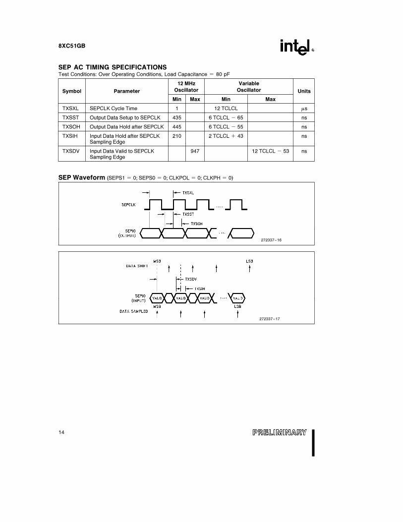
SEP AC TIMING SPECIFICATIONSTest Conditions: Over Operating Conditions, Load Capacitance e 80 pF
Symbol Parameter
12 MHz Variable
UnitsOscillator Oscillator
Min Max Min Max
TXSXL SEPCLK Cycle Time 1 12 TCLCL ms
TXSST Output Data Setup to SEPCLK 435 6 TCLCL b 65 ns
TXSOH Output Data Hold after SEPCLK 445 6 TCLCL b 55 ns
TXSIH Input Data Hold after SEPCLK 210 2 TCLCL a 43 nsSampling Edge
TXSDV Input Data Valid to SEPCLK 947 12 TCLCL b 53 nsSampling Edge
SEP Waveform (SEPS1 e 0; SEPS0 e 0; CLKPOL e 0; CLKPH e 0)
272337–16
272337–17
14

8XC51GB
AC TESTING INPUT, OUTPUT WAVEFORMS
272337–18
AC inputs during testing are driven at VCCb0.5V for a Logic‘‘1’’ and 0.5V for a Logic ‘‘0’’. Timing measurements aremade at VIH for a Logic ‘‘1’’ and VOL max for a Logic ‘‘0’’.
FLOAT WAVEFORMS
272337–19
For timing purposes a port pin is no longer floatingwhen a 100 mV change from load voltage occurs,and begins to float when a 100 mV change fromthe loaded VOH/VOL level occurs. IOL/IOH t g20mA.
A TO D CHARACTERISTICS
The absolute conversion accuracy is dependent onthe accuracy of AVREF. The specifications given be-low assume adherence to the Operating Conditionssection of this data sheet. Testing is done atAVREF e 5.12V, and VCC e 5.0V.
OPERATING CONDITIONS
VCC ÀÀÀÀÀÀÀÀÀÀÀÀÀÀÀÀÀÀÀÀÀÀÀÀÀÀÀÀÀÀÀ4.0V to 6.0V
AVREF ÀÀÀÀÀÀÀÀÀÀÀÀÀÀÀÀÀÀÀÀÀÀÀÀÀÀÀÀÀ4.5V to 5.5V
VSS, AVSS ÀÀÀÀÀÀÀÀÀÀÀÀÀÀÀÀÀÀÀÀÀÀÀÀÀÀÀÀÀÀÀÀÀÀ0V
ACH0–7 ÀÀÀÀÀÀÀÀÀÀÀÀÀÀÀÀÀÀÀÀÀÀÀÀÀÀAVSS to VREF
TA ÀÀÀÀÀÀÀÀÀÀÀÀÀÀÀÀÀÀÀÀÀÀÀ0§C to a70§C Ambient
FOSC (STD Version)ÀÀÀÀÀÀÀÀÀÀÀ3.5 MHz to 12 MHz
FOSC (-1 Version) ÀÀÀÀÀÀÀÀÀÀÀÀÀ3.5 MHz to 16 MHz
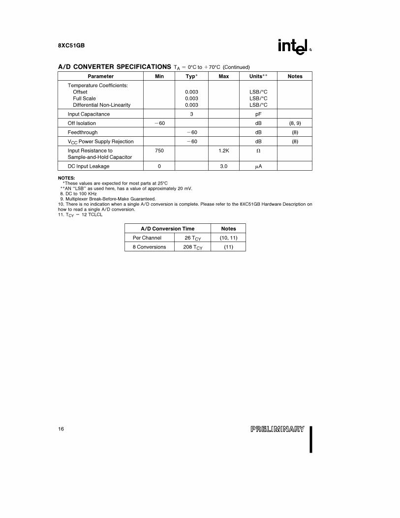
A/D CONVERTER SPECIFICATIONS TA e 0§C to a70§CParameter Min Typ* Max Units** Notes
Resolution 256 256 Levels
8 8 Bits
Absolute Error (Ch 2–7) 0 g1 LSB
Absolute Error (Ch 0 and 1) 0 g2 LSB
Full Scale Error g1 LSB
Zero Offset Error g1 LSB
Non-Linearity 0 g1 LSB
Differential Non-Linearity 0 g1 LSB
Channel-to-Channel Matching 0 g1 LSB
Repeatability g0.25 LSB
15
8XC51GB
A/D CONVERTER SPECIFICATIONS TA e 0§C to a70§C (Continued)
Parameter Min Typ* Max Units** Notes
Temperature Coefficients:
Offset 0.003 LSB/§CFull Scale 0.003 LSB/§CDifferential Non-Linearity 0.003 LSB/§C
Input Capacitance 3 pF
Off Isolation b60 dB (8, 9)
Feedthrough b60 dB (8)
VCC Power Supply Rejection b60 dB (8)
Input Resistance to 750 1.2K XSample-and-Hold Capacitor
DC Input Leakage 0 3.0 mA
NOTES:*These values are expected for most parts at 25§C
**AN ‘‘LSB’’ as used here, has a value of approximately 20 mV.8. DC to 100 KHz9. Multiplexer Break-Before-Make Guaranteed.
10. There is no indication when a single A/D conversion is complete. Please refer to the 8XC51GB Hardware Description onhow to read a single A/D conversion.11. TCY e 12 TCLCL
A/D Conversion Time Notes
Per Channel 26 TCY (10, 11)
8 Conversions 208 TCY (11)
16

8XC51GB
PROGRAMMING THE OTP
The part must be running with a 4 MHz to 6 MHzoscillator. The address of a location to be pro-grammed is applied to address lines while the codebyte to be programmed in that location is applied todata lines. Control and program signals must be heldat the levels indicated in Table 2. Normally EA/VPPis held at logic high until just before ALE/PROG is tobe pulsed. The EA/VPP is raised to VPP, ALE/PROGis pulsed low and then EA/VPP is returned to a high(also refer to timing diagrams).
NOTE:Exceeding the VPP maximum for any amount oftime could damage the device permanently. TheVPP source must be well regulated and free ofglitches.
DEFINITION OF TERMS
ADDRESS LINES: P1.0–P1.7, P2.0–P2.4, respec-tively for A0–A12.
DATA LINES: P0.0–P0.7 for D0–D7.
CONTROL SIGNALS: RST, PSEN, P2.6, P2.7, P3.3,P3.6, P3.7
PROGRAM SIGNALS: ALE/PROG, EA/VPP
272337–20*See Table 2 for proper input on these pins.
Figure 11. Programming the OTP
Table 2. OTP Programming Modes
Mode RST PSENALE/ EA/
P2.6 P2.7 P3.3 P3.6 P3.7PROG VPP
Program Code Data L L ß 12.75V L H H H H
Verify Code Data L L H H L L L H H
Program Encryption L L ß 12.75V L H H L H
Array Address 0–3FH
Program Lock Bit 1 L L ß 12.75V H H H H H
BitsBit 2 L L ß 12.75V H H H L L
Bit 3 L L ß 12.75V H L H H L
Read Signature Byte L H H H L L L L L
17

8XC51GB
PROGRAMMING ALGORITHM
Refer to Table 2 and Figures 11 and 12 for address,data, and control signals set up. To program the87C51GB the following sequence must be exer-cised.
1. Input the valid address on the address lines.
2. Input the appropriate data byte on the data lines.
3. Activate the correct combination of control sig-nals.
4. Raise EA/VPP from VCC to 12.75V g0.25V.
5. Pulse ALE/PROG 5 times for the OTP array, and25 times for the encryption table and the lockbits.
Repeat 1 through 5 changing the address and datafor the entire array or until the end of the object file isreached.
PROGRAM VERIFY
Program verify may be done after each byte that isprogrammed, or after a block of bytes that is pro-grammed. In either case a complete verify of thearray will ensure that it has been programmed cor-rectly.
The lock bits cannot be directly verified. Verificationof the lock bits is done by observing that their fea-tures are enabled. Refer to the Program Lock sec-tion in this data sheet.
272337–21
Figure 12. Programming Signal’s Waveforms
18

8XC51GB
ROM and EPROM Lock System
The 87C51GB and the 83C51GB program lock sys-tems, when programmed, protect the on-board pro-gram against software piracy.
The 83C51GB has a one-level program lock systemand a 64-byte encryption table. See line 2 of Table3. If program protection is desired, the user submitsthe encryption table with their code, and both thelock bit and encryption array are programmed by thefactory. The encryption array is not available withoutthe lock bit. For the lock bit to be programmed, theuser must submit an encryption table.
The 87C51GB has a 3-level program lock systemand a 64-byte encryption array. Since this is anEPROM device, all locations are user programma-ble. See Table 3.
Encryption Array
Within the programmable array are 64 bytes of En-cryption Array that are initially unprogrammed (all1’s). Every time that a byte is addressed during averify, 5 address lines are used to select a byte ofthe Encryption Array. This byte is then exclusive-NOR’ed (XNOR) with the code byte, creating an En-cryption Verify byte. The algorithm, with the array inthe unprogrammed state (all 1’s), will return thecode in its original, unmodified form. For program-ming the Encryption Array, refer to Table 2.
When using the encryption array feature, one impor-tant factor needs to be considered. If a code bytehas the value 0FFH, verification of the byte will pro-duce the encryption byte value. If a large block (l64bytes) of code is left unprogrammed, a verificationroutine will display the contents of the encryptionarray. For this reason it is strongly recommendedthat all unused code bytes be programmed withsome value other than 0FFH, and not all of them thesame value. This practice will ensure the maximumpossible program protection.
Program Lock Bits
The 87C51GB has 3 programmable lock bits thatwhen programmed according to Table 3 will providedifferent levels of protection for the on-chip codeand data. The 83C51GB has 1 program lock bit.See line 2 of Table 3.
Reading the Signature Bytes
The 8XC51GB has 3 signature bytes in locations30H, 31H, and 60H. To read these bytes follow theprocedure for verify, but activate the control linesprovided in Table 2 for Read Signature Byte.
LocationContents
87C51GB 83C51GB
30H 89H 89H
31H 58H 58H
60H EBH EBH/6BH
Table 3. Program Lock Bits and the Features
*Program Lock BitsProtection Type
LB1 LB2 LB3
1 U U U No Program Lock features enabled. (Code verify willstill be encrypted by the Encryption Array ifprogrammed).
2 P U U MOVC instructions executed from external programmemory are disabled from fetching code bytes frominternal memory, EA is sampled and latched onReset, and further programming of the EPROM isdisabled.
3 P P U Same as 2, also verify is disabled.
4 P P P Same as 3, also external execution is disabled.
*Any other combination of lock bits is not defined.
19

8XC51GB
OTP PROGRAMMING AND VERIFICATION CHARACTERISTICS(TA e 21§C to 27§C; VCC e 5V g 20%; VSS e 0V)
Symbol Parameter Min Max Units
VPP Programming Supply Voltage 12.5 13.0 V
IPP Programming Supply Current 75 mA
1/TCLCL Oscillator Frequency 4 6 MHz
TAVGL Address Setup to PROG Low 48TCLCL
TGHAX Address Hold after PROG 48TCLCL
TDVGL Data Setup to PROG Low 48TCLCL
TGHDX Data Hold after PROG 48TCLCL
TEHSH (Enable) High to VPP 48TCLCL
TSHGL VPP Setup to PROG Low 10 ms
TGHSL VPP Hold after PROG 10 ms
TGLGH PROG Width 90 110 ms
TAVQV Address to Data Valid 48TCLCL
TELQV ENABLE Low to Data Valid 48TCLCL
TEHQZ Data Float after ENABLE 0 48TCLCL
TGHGL PROG High to PROG Low 10 ms
PROGRAMMING AND VERIFICATION WAVEFORMS
272337–22
*25 Pulses for Encryption Table and Lock Bits.
20
8XC51GB
A/D Glossary of Terms
Absolute ErrorÐThe maximum difference betweencorresponding actual and ideal code transitions. Ab-solute Error accounts for all deviations of an actualconverter from an ideal converter.
Actual CharacteristicÐThe characteristic of an ac-tual converter. The characteristic of a given convert-er may vary over temperature, supply voltage, andfrequency conditions. An actual characteristic rarelyhas ideal first and last transition locations or idealcode widths. It may even vary over multiple conver-sions under the same conditions.
Break-Before-MakeÐThe property of a multiplexerwhich guarantees that a previously selected channelwill be deselected before a new channel is selected(e.g., the converter will not short inputs together).
Channel-to-Channel MatchingÐThe difference be-tween corresponding code transitions of actual char-acteristics taken from different channels under thesame temperature, voltage and frequency condi-tions.
CharacteristicÐA graph of input voltage versus theresultant output code for an A/D converter. It de-scribes the transfer function of the A/D converter.
CodeÐThe digital value output by the converter.
Code CenterÐThe voltage corresponding to themidpoint between two adjacent code transitions.
Code TransitionÐThe point at which the converterchanges from an output code of Q, to a code of Q a
1. The input voltage corresponding to a code tran-sition is defined to be that voltage which is equallylikely to produce either of two adjacent codes.
Code WidthÐThe voltage corresponding to the dif-ference between two adjacent code transitions.
CrosstalkÐSee ‘‘Off-Isolation’’.
DC Input LeakageÐLeakage current to groundfrom an analog input pin.
Differential Non-LinearityÐThe difference be-tween the ideal and actual code widths of the termi-nal based characteristic.
FeedthroughÐAttenuation of a voltage applied onthe selected channel of the A/D Converter after thesample window closes.
Full Scale ErrorÐThe difference between the ex-pected and actual input voltage corresponding tothe full scale code transition.
Ideal CharacteristicÐA characteristic with its firstcode transition at VIN e 0.5 LSB, its last code tran-sition at VIN e (VREF b 1.5 LSB) and all codewidths equal to one LSB.
Input ResistanceÐThe effective series resistancefrom the analog input pin to the sample capacitor.
LSBÐLeast Significant BitÐThe voltage corre-sponding to the full scale voltage divided by 2n,where n is the number of bits of resolution of theconverter. For an 8-bit converter with a referencevoltage of 5.12V, one LSB is 20 mV. Note that this isdifferent than digital LSBs since an uncertainty oftwo LSBs, when referring to an A/D converter,equals 40 mV. (This has been confused with an un-certainty of two digital bits, which would mean fourcounts, or 80 mV).
MonotonicÐThe property of successive approxi-mation converters which guarantees that increasinginput voltages produce adjacent codes of increasingvalue, and that decreasing input voltages produceadjacent codes of decreasing value.
No Missed CodesÐFor each and every outputcode, there exists a unique input voltage rangewhich produces that code only.
Non-LinearityÐThe maximum deviation of codetransitions of the terminal based characteristic fromthe corresponding code transitions of the ideal char-acteristic.
Off-IsolationÐAttenuation of a voltage applied on adeselected channel of the A/D converter. (Also re-ferred to as Crosstalk.)
RepeatabilityÐThe difference between corre-sponding code transitions from different actual char-acteristics taken from the same converter on thesame channel at the same temperature, voltage andfrequency conditions.
ResolutionÐThe number of input voltage levelsthat the converter can unambiguously distinguishbetween. Also defines the number of useful bits ofinformation which the converter can return.
Sample DelayÐThe delay from receiving the startconversion signal to when the sample windowopens.
Sample Delay UncertaintyÐThe variation in thesample delay.
Sample TimeÐThe time that the sample window isopen.
Sample Time UncertaintyÐThe variation in thesample time.
21

8XC51GB
Sample WindowÐBegins when the sample capaci-tor is attached to a selected channel and ends whenthe sample capacitor is disconnected from the se-lected channel.
Successive ApproximationÐAn A/D conversionmethod which uses a binary search to arrive at thebest digital representation of an analog input.
Temperature CoefficientsÐChange in the statedvariable per degree centrigrade temperaturechange. Temperature coefficients are added to thetypical values of a specification to see the effect oftemperature drift.
Terminal Based CharacteristicÐAn actual charac-teristic which has been rotated and translated to re-move zero offset and full scale error.
VCC RejectionÐAttenuation of noise on the VCCline to the A/D converter.
Zero OffsetÐThe difference between the expectedand actual input voltage corresponding to the firstcode transition.
DATA SHEET REVISION SUMMARY
The following differences exist between this data-sheet and the previous version (270869-003):
1. Merged 87C51GB Express (270889-001).
2. New order number 272337-001.
The following differences exist between the 270869-003 data sheet and the previous version (270869-002):
1. Changed data sheet status from ‘‘Advance Infor-mation’’ to ‘‘Preliminary’’ and updated associatednotices.
2. Added 83C51GB throughout.
3. Added Package and Process Information.
4. Clarified g2 LSB accuracy for channels 0 and 1in A/D Converter Section.
5. Added ‘‘ROM and EPROM Lock System’’ sectionand added 83C51GB to ‘‘Program Lock Bits’’section.
6. Modified Signature Bytes Table.
The following differences exist between the270869-002 data sheet and the previous version(270869-001):
1. Changed data sheet status from ‘‘Product Pre-view’’ to ‘‘Advance Information’’ and updated as-sociated notices.
2. Asynchronous port reset was added to RESETpin description.
3. ALE disable paragraph was added to ALE pin de-scription.
4. C1, C2 guidelines clarified in Figure 4.
5. Operating Conditions heading was added.
6. Maximum IOL per I/O pin was added to AbsoluteMaximum Ratings.
7. VTa, VTb, VHYS, VOL2, and VTL removed.
8. VOL value for ALE included with VOL1.
9. VIL1 and VIL2 added.
10. RRST minimum changed from 40K to 50K.RRST maximum changed from 225K to 300K.
11. IPD maximum changed from 200 mA to 50 mA.
12. IDL maximum changed from 15 mA to 18 mA.
13. Typical values for IPD, IDL, ICC, and IREF re-moved.
14. Note 3 (page 9) was reworded.
15. SEP AC Timings added.
16. A/D Absolute Error for Channels 0 and 1changed to g2 LSB.
17. TCY clarified.
18. Encryption array paragraph was added.
19. Corrected pin numbers on Figure 11 to reflectPLCC package.
22