Embed Size (px)
Citation preview

F2-08DA-1, 8-ChAnnel AnAlog Current output 71010
ChapterChapterChapter
In This Chapter...Module Specifications 10–2
Connecting and Disconnecting the Field Wiring 10–5
Module Operation 10–7
Writing the Control Program 10–11

DL205 Analog Manual, 7th Edition Rev. D10-2
Chapter 10: F2-08DA-1, 8-Channel Analog Current Output
1
2
3
4
5
6
7
8
9
10
11
12
13
14
A
B
C
D
Module SpecificationsThe F2-08DA-1 Analog Output module provides several hardware features:
• Supported by DL230, DL240, DL250-1 and DL260 CPUs (see firmware requirements).
• Analog outputs are optically isolated from the PLC logic.
• The module has a removable terminal block so the module can be easily removed or changed without disconnecting the wiring.
• All channels can be updated in one scan (DL240, DL250-1 and DL260 only).
• Outputs are both current sinking and sourcing.
Firmware Requirements:• To use this module, DL230 CPUs must have firmware version 2.7 or later.
• To use the pointer method for writing values, DL240 CPUs require firmware version 3.0 or later.
• DL250 CPUs require firmware version 1.33 or later.
Analog Output Configuration RequirementsThe F2-08DA-1 Analog output 16-point output points. The module can be installed in any slot of a DL205 PLC system, but the available power budget and discrete I/O points can be the limiting factors. Check the user manual for the particular model of CPU and I/O base being used for information regarding power budget and number of local, local expansion or remote I/O points.
1
2
3
4
5
6
7
8
9
10
11
12
13
14
A
B
C
D
OUT
F2-08DA-1
ANALOG8 CHANNEL
18-26.4VDC80mA4-20mASNK-SRC
1-O
2-O
3-O
4-O
5-O
6-O
7-O
8-O
0V
1-I
2-I
3-I
4-I
5-I
6-I
7-I
8-I
N/C
24V
F2-08DA-1

DL205 Analog Manual, 7th Edition Rev. D 10-3
Chapter 10: F2-08DA-1, 8-Channel Analog Current Output
1
2
3
4
5
6
7
8
9
10
11
12
13
14
A
B
C
D
The following tables provide the specifications for the F2–08DA–1 Analog Output Module. Review these specifications to make sure the module meets your application requirements.
NOTE: One count in the specifications table is equal to one least significant bit of the analog data value (1 in 4096)
Output Specifications Number of Channels 8, single-ended Output Range 4–20 mA Resolution 12 bit (1 in 4096) Output Type Current sinking and current sourcing Maximum Loop Supply 30VDC Source Load 0 – 400q (for loop power 18 – 30V) Sink Load 0 – 600q / 18V, 900q / 24V, 1200q / 30V Total Load (sink plus source) 600q / 18V, 900q / 24V, 1200q / 30V Linearity Error (end to end) ±2 counts (±0.050% of full scale) maximum Conversion Settling Time 400µs maximum (full scale change)
Full-scale Calibration Error ±12 counts maximum, sinking (any load) ±12 counts maximum, sourcing (125q load) ±18 counts maximum, sourcing (250q load) ±26 counts maximum, sourcing (400q load)
Offset Calibration Error ±9 counts maximum, sinking (any load) ±9 counts maximum, sourcing (125q load) ±11 counts maximum, sourcing (250q load) ±13 counts maximum, sourcing (400q load)
Maximum Full Scale Inaccuracy @ 0–60°C 0.5% sinking (any load) & sourcing (125q load ) 0.64% sourcing (250q load ) 0.83% sourcing (400q load)
Maximum Full Scale Inaccuracy @ 0–25°C (includes all errors & temperature drift)
0.3% sinking (any load) & sourcing (125q load ) 0.44% sourcing (250q load ) 0.63% sourcing (400q load)
1
2
3
4
5
6
7
8
9
10
11
12
13
14
A
B
C
D
General Specifications PLC Update Rate 8 channel per scan maximum Digital Outputs / Output Points Required
12 binary data bits, 3 channel ID bits, 1 output enable bit / 16 (Y) output points required
Power Budget Requirement 30mA @ 5VDC (supplied by the base) External Power Supply 18–30 VDC, 50mA plus 20mA / output loop, class 2 Operating Temperature 0–60°C (32–140°F) Storage Temperature -20–70°C (-4–158°F) Relative Humidity 5–95% (non-condensing) Environmental air No corrosive gases permitted Vibration MIL STD 810C 514.2 Shock MIL STD 810C 516.2 Noise Immunity NEMA ICS3-304

DL205 Analog Manual, 7th Edition Rev. D10-4
Chapter 10: F2-08DA-1, 8-Channel Analog Current Output
1
2
3
4
5
6
7
8
9
10
11
12
13
14
A
B
C
D
Special Placement Requirements (DL230 and Remote I/O Bases)It is important to examine the configuration if a DL230 CPU is being used. As can be seen in the section on Writing the Control Program, V-memory locations are used to capture the analog data. If the module is placed in a slot so that the output points do not start on a V-memory boundary, the program instructions aren’t able to access the data. This also applies when placing this module in a remote base using a D2-RSSS in the CPU slot.
To use the V-memory references required for the multiplexing method, the first output address assigned to the module must be one of the following Y locations. The table also shows the V-memory addresses that correspond to these Y locations.
1
2
3
4
5
6
7
8
9
10
11
12
13
14
A
B
C
D X Y0 Y20 Y40 Y60 Y100 Y120 Y140 Y160 V V40500 V40501 V40502 V40503 V40504 V40505 V40506 V40507
Y37
F2-08DA-1
V40501BSLBSM
Y20
V40500 V40502
Correct!
16ptInput
8ptInput
16ptOutput Output
8pt16ptOutput
X0--X17
X20--X27
Y0--Y17
Y20--Y37
Y40--Y47
Slot 0 Slot 1 Slot 2 Slot 3 Slot 4
Y27
Y30
Data is correctly entered so output points start on a V-memory boundary address from the table below.
16ptInput
8ptInput
8ptOutput Output
16pt16ptOutput
X0--X17
X20--X27
Y0--Y17
Y20--Y27
Y30--Y47
F2-08DA-1
V40502 BSLBSM
Y40
Y57
Y47
Y50
V40501 BSLBSM
Y20
Y37
Y27
Y30
Incorrect
Slot 0 Slot 1 Slot 2 Slot 3 Slot 4
Data is split over two locations, so instructions cannot access data from a DL230 (or when the module is placed in a remote base).

DL205 Analog Manual, 7th Edition Rev. D 10-5
Chapter 10: F2-08DA-1, 8-Channel Analog Current Output
1
2
3
4
5
6
7
8
9
10
11
12
13
14
A
B
C
D
Connecting and Disconnecting the Field WiringWiring Guidelines
Your company may have guidelines for wiring and cable installation. If so, check the guidelines before beginning the installation. Here are some general things to consider:
• Use the shortest wiring route whenever possible.
• Use shielded wiring and ground the shield at the transmitter source. Do not ground the shield at both the module and the source.
• Do not run the signal wiring next to large motors, high current switches, or transformers. This may cause noise problems.
• Route the wiring through an approved cable housing to minimize the risk of accidental damage. Check local and national codes to choose the correct method for your application.
User Power Supply RequirementsThe F2-08DA-1 requires an external power supply. The same or separate power sources may be used for the module supply and loop supply. The module requires 18–30 VDC, at 50mA. The two current loops also require 18–30 VDC, but at 20mA each.
The DL205 bases have internal 24VDC power supplies that provide up to 300mA of current. This power source can be used instead of a separate power supply if only a few analog modules are being used. The current required will be 50mA (module) plus 160mA (eight loops) for a total of 210mA.
It is desirable in some situations to power the transmitters separately in a location remote from the PLC. This will work as long as the transmitter supply meets the voltage and current requirements and the transmitter’s minus (-) side and the module supply’s minus (-) side are connected together.
WARNING: If the internal 24VDC power budget is exceeded, it may cause unpredictable system operation that can lead to a risk of personal injury or equipment damage.
1
2
3
4
5
6
7
8
9
10
11
12
13
14
A
B
C
D

DL205 Analog Manual, 7th Edition Rev. D10-6
Chapter 10: F2-08DA-1, 8-Channel Analog Current Output
1
2
3
4
5
6
7
8
9
10
11
12
13
14
A
B
C
D
Wiring DiagramThe F2-08DA-1 module has a removable connector which helps to simplify wiring. Just squeeze the top and bottom retaining clips and gently pull the connector from the module. Use the following diagram to connect the field wiring. Channels 1 and 2 are shown wired for sourcing, and channels 7 and 8 are shown wired for sinking. The diagram also shows how to wire an optional loop power supply.
NOTE 1: Shields should be connected to the 0V terminal of the module.
Load RangeThe maximum load resistance depends on the particular loop power supply being used.
1
2
3
4
5
6
7
8
9
10
11
12
13
14
A
B
C
D
OUT
F2-08DA-1
ANALOG8 CHANNEL
18-26.4VDC80mA4-20mASNK-SRC
1-O
2-O
3-O
4-O
5-O
6-O
7-O
8-O
0V
1-I
2-I
3-I
4-I
5-I
6-I
7-I
8-I
N/C
24V
SeeNOTE 1
Typical User Wiring
SOURCEConfigurations
SINKConfigurations
Ch 1 load250 ohms typical
Ch 2 load250 ohms typical
Ch 7 load250 ohms typical
Ch 8 load250 ohms typical
18-30 VDC
+ –
InternalModule Wiring
Sink/Source Circuitry1–O
2–O
3–O
4–O
5–O
6–O
7–O
8–O
0V
1–I
2–I
3–I
4–I
5–I
6–I
7–I
8–I
N/C
24V
Loop Power Supply Voltage Source Load Range Sink Load Range30VDC
0 – 400q0 – 1200q
24VDC 0 – 900q18VDC 0 – 600q

DL205 Analog Manual, 7th Edition Rev. D 10-7
Chapter 10: F2-08DA-1, 8-Channel Analog Current Output
1
2
3
4
5
6
7
8
9
10
11
12
13
14
A
B
C
D
Module OperationBefore beginning to write the control program, it is important to take a few minutes to under-stand how the module processes the analog signals.
Channel Scanning Sequence for a DL230 CPU (Multiplexing)The DL230 can send one channel of data to the output per CPU scan if the multiplexing method is used. The module refreshes all field devices on each scan, but new data can only be obtained from the CPU at the rate of one channel per scan. Since there are eight channels, it can take eight scans to update all channels. However, if only one channel is being used, then that channel will be updated on every scan. The multiplexing method can also be used for the DL240, DL250-1, and DL260 CPUs.
1
2
3
4
5
6
7
8
9
10
11
12
13
14
A
B
C
D
Channel 1
Channel 2
Channel 3
Channel 4
Channel 8
Scan N
Calculate the data
Write data
Read inputs
Execute Application ProgramScan N+1
Scan N+2
Scan N+3
Scan N+8
Scan
Write to outputs
System UsingMultiplexMethod(DL230)
.
.
.
.
.
.

DL205 Analog Manual, 7th Edition Rev. D10-8
Chapter 10: F2-08DA-1, 8-Channel Analog Current Output
1
2
3
4
5
6
7
8
9
10
11
12
13
14
A
B
C
D
Channel Scanning Sequence for DL240, DL250-1, and DL260 CPUs (Pointer Method)
If either a DL240, DL250-1 or a DL260 CPU is used, all channels can be updated on every scan. This is because the all three CPUs support special V-memory locations that are used to manage the data transfer. This is discussed in more detail in the next section on Writing the Control Program.
Understanding the Output AssignmentsRemember that the F2-08DA-1 module appears to the CPU as a 16-point discrete output module. These points provide the data value and an indication of which channel to update. Note, if either a DL240, DL250 or a DL260 CPU is being used, these bits may never have to be used, but it may be an aid to help understand the data format.
Since all output points are automatically mapped into V-memory, the location of the data word that will be assigned to the module can be simply determined.
1
2
3
4
5
6
7
8
9
10
11
12
13
14
A
B
C
D
Channel 1, 2...8
Channel 1, 2...8
Channel 1, 2...8
Channel 1, 2...8Scan N
Calculate the data
Write data
Read inputs
Execute Application ProgramScan N+1
Scan N+2
Scan N+3
Scan N+4
Scan
Write to outputs
System WithDL240/250--1/260CPU Using Point-
er Method
Channel 1, 2...8

DL205 Analog Manual, 7th Edition Rev. D 10-9
Chapter 10: F2-08DA-1, 8-Channel Analog Current Output
1
2
3
4
5
6
7
8
9
10
11
12
13
14
A
B
C
D
The individual bits in this data word location, represents specific information about the analog signal.
Channel Select OutputsThree of the outputs select the active channel. Remember, the V-memory bits are mapped directly to discrete outputs. The binary weight of the three bits will determine the selected bit. By controlling these outputs, the channel to be updated can be selected.
1
2
3
4
5
6
7
8
9
10
11
12
13
14
A
B
C
D
Y20Data Bits
Y35
Y34
F2-08DA--1
V40501BSLBSM
V40500 V40502
16ptInput
8ptInput
16ptOutput Output
8pt16ptOutput
X0--X17
X20--X27
Y0--Y17
Y20--Y37
Y40--Y47
Slot 0 Slot 1 Slot 2 Slot 3 Slot 4
Y37
Y36
= channel select outputs
Y35
V40501BSLBSM
Y20
Y34
Y36
Select Channel Outputs
Y36 Y35 Y34 Channel Number Selected
– – – 1– – X 2– X – 3– X X 4X – – 5X – X 6X X – 7X X X 8
DL205 Analog Manual, 7th Edition Rev. D10-10
Chapter 10: F2-08DA-1, 8-Channel Analog Current Output
1
2
3
4
5
6
7
8
9
10
11
12
13
14
A
B
C
D
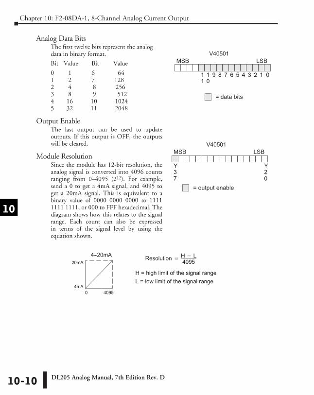
Analog Data BitsThe first twelve bits represent the analog data in binary format.
Bit Value Bit Value
0 1 6 64 1 2 7 128 2 4 8 256 3 8 9 512 4 16 10 1024 5 32 11 2048
Output EnableThe last output can be used to update outputs. If this output is OFF, the outputs will be cleared.
Module ResolutionSince the module has 12-bit resolution, the analog signal is converted into 4096 counts ranging from 0–4095 (212). For example, send a 0 to get a 4mA signal, and 4095 to get a 20mA signal. This is equivalent to a binary value of 0000 0000 0000 to 1111 1111 1111, or 000 to FFF hexadecimal. The diagram shows how this relates to the signal range. Each count can also be expressed in terms of the signal level by using the equation shown.
1
2
3
4
5
6
7
8
9
10
11
12
13
14
A
B
C
D
V40501BSLBSM
011109 8 7 6 5 4 3 2 1
= data bits
= output enable
Y37
V40501BSLBSM
Y20
20mA
4mA0 4095
4--20mA Resolution = H− L4095
H = high limit of the signal rangeL = low limit of the signal range

DL205 Analog Manual, 7th Edition Rev. D 10-11
Chapter 10: F2-08DA-1, 8-Channel Analog Current Output
1
2
3
4
5
6
7
8
9
10
11
12
13
14
A
B
C
D
Writing the Control ProgramCalculating the Digital Value
The control program must calculate the digital value that is sent to the analog output. Several methods can be used to do this, but the best method is to convert the values to engineering units. This is accomplished by using the formula shown.
Adjustments may have to be made to the formula depending on the scale of the engi-neering units.
Consider the following example which controls pressure from 0.0–99.9 PSI. Using the formula will calculate the digital value to be sent to the analog output. The example shows the conversion required to yield 49.4 PSI. The multiplier of 10 is used because the decimal portion of 49.4 cannot be loaded in the program, so it is shifted right one decimal place to make a usable value of 494.
The Conversion ProgramThe example program shows how to write the program to perform the engineering unit conversion. This example assumes that a BCD value has been stored in V2300 and V2301 for channels 1 and 2 respectively.
NOTE: The DL205 has many instructions available so that math operations can simply be performed using BCD format. Do the math in BCD, then convert to binary before writing to the module output.
1
2
3
4
5
6
7
8
9
10
11
12
13
14
A
B
C
D
For 0–4095 output format A = U 4095 H – L
A = Analog Value (0–4095)
U = Engineering Units
H = High limit of the engineering unit range
L = Low limit of the engineering unit range
The LD instruction loads the engineering units used with channel 1 intothe accumulator. This example assumes the numbers are BCD. SinceSP1 is used, this rung automatically executes on every scan. You couldalso use an X, C, etc. permissive contact.
LDV2300
SP1
MULK4095
DIVK1000
Multiply the accumulator by 4095 (to start the conversion).
Divide the accumulator by 1000 (because we used a multiplier of 10,we have to use 1000 instead of 100).
OUTV2000
Store the BCD result in V2000 (the actual steps required to send thedata are shown later).
The LD instruction loads the engineering units used with channel 2 intothe accumulator. This example assumes the numbers are BCD. SinceSP1 is used, this rung automatically executes on every scan. You couldalso use an X, C, etc. permissive contact.
LDV2301
SP1
MULK4095
DIVK1000
Multiply the accumulator by 4095 (to start the conversion).
Divide the accumulator by 1000 (because we used a multiplier of 10,we have to use 1000 instead of 100).
OUTV2001
Store the BCD result in V2001 (the actual steps required to send thedata are shown later).
A = 10U 4095 A = 494 4095 A–2023 10 (H–L) 1000–0)

DL205 Analog Manual, 7th Edition Rev. D10-12
Chapter 10: F2-08DA-1, 8-Channel Analog Current Output
1
2
3
4
5
6
7
8
9
10
11
12
13
14
A
B
C
D
Reading Values Pointer Method and MultiplexingTwo methods are used to read data values in the DL205, pointer and multiplexing methods. When to use either method and how to use it will be discussed here. Since the pointer method will not work if the PLC has a DL230 installed, only the multiplexing method can be used. Either method for reading the data values can be used with the DL240, DL250-1 and DL260 CPUs, however, the pointer method will simplify programming the PLC.
Pointer Method for the DL240, DL250-1 and DL260 CPUsOnce the data values have been calculated they must be entered into the program in order to output the values. The DL205 series has special V-memory locations assigned to each base slot that will greatly simplify the programming requirements. With these V-memory locations, the number of channels to update are specified, also, where to read the data that is written to the output is specified.
NOTE: DL240 CPUs with firmware release version 1.5 or later and. DL250 CPUs with firmware release version 1.06 or later support this method.
The following example program shows how to setup these locations. Place this rung anywhere in the ladder program, or in the initial stage if stage programming instructions are being used. This is all that is required to write the data to V-memory locations. Once the data has been written to V-memory math can be used on the data, compare the data against preset values, etc. V2000 is used in the example but any user V-memory location can be used. In this example the module is installed in slot 2. Be sure to use the V-memory locations for the module placement. The pointer method automatically converts values to BCD.
1
2
3
4
5
6
7
8
9
10
11
12
13
14
A
B
C
D
SP0LDK
LDAO2000
OUTV7703
This loads an octal value for the first V-memory location that will beused to store the output data. For example, the O2000 entered herewould designate the following addresses.Ch1 -- V2000, Ch2 -- V2001
OUTV7663
Special V-memory location assigned to slot 3 that contains thenumber of channels to scan.
LD
Loads a constant that specifies the number of channels to scan andthe data format. The lower byte, most significant nibble (MSN)selects the data format (i.e. 0=BCD, 8=Binary), the LSN selects thenumber of channels (1 or 2).
- or -
The binary format is used for displaying data on some operatorinterfaces. The DL230/240 CPUs do not support binary mathfunctions, whereas the DL250 does.
2 K 82
The octal address (O2000) is stored here. V7703 is assigned to slot3 and acts as a pointer, which means the CPU will use the octalvalue in this location to determine exactly where to store the outputdata.

DL205 Analog Manual, 7th Edition Rev. D 10-13
Chapter 10: F2-08DA-1, 8-Channel Analog Current Output
1
2
3
4
5
6
7
8
9
10
11
12
13
14
A
B
C
D
The following tables show the special V-memory locations used by the DL240, DL250-1 and DL260 for the CPU base and local expansion base I/O slots. Slot 0 (zero) is the module next to the CPU or D2-CM module. Slot 1 is the module two places from the CPU or D2-CM, and so on. Remember, the CPU only examines the pointer values at these locations after a mode transition. Also, if the DL230 (multiplexing) method is used, verify that these addresses in the CPU are 0 (zero).
The table below applies to the DL240, DL250-1 and DL260 CPU base.
1
2
3
4
5
6
7
8
9
10
11
12
13
14
A
B
C
D
CPU Base: Analog Output Module Slot-Dependent V-memory LocationsSlot 0 1 2 3 4 5 6 7No. of Channels V7660 V7661 V7662 V7663 V7664 V7665 V7666 V7667Storage Pointer V7700 V7701 V7702 V7703 V7704 V7705 V7706 V7707
Expansion Base D2-CM #1: Analog Output Module Slot-Dependent V-memory LocationsSlot 0 1 2 3 4 5 6 7No. of Channels V36000 V36001 V36002 V36003 V36004 V36005 V36006 V36007Storage Pointer V36020 V36021 V36022 V36023 V36024 V36025 V36026 V36027
Expansion Base D2-CM #2: Analog Output Module Slot-Dependent V-memory LocationsSlot 0 1 2 3 4 5 6 7No. of Channels V36100 V36101 V36102 V36103 V36104 V36105 V36106 V36107Storage Pointer V36120 V36121 V36122 V36123 V36124 V36125 V36126 V36127
Expansion Base D2-CM #3: Analog Output Module Slot-Dependent V-memory LocationsSlot 0 1 2 3 4 5 6 7No. of Channels V36200 V36201 V36202 V36203 V36204 V36205 V36206 V36207Storage Pointer V36220 V36221 V36222 V36223 V36224 V36225 V36226 V36227
Expansion Base D2-CM #4: Analog Output Module Slot-Dependent V-memory LocationsSlot 0 1 2 3 4 5 6 7No. of Channels V36300 V36301 V36302 V36303 V36304 V36305 V36306 V36307Storage Pointer V36320 V36321 V36322 V36323 V36324 V36325 V36326 V36327
The table below applies to the DL250-1 or the DL260 CPU base 1.
The table below applies to the DL250-1 or the DL260 CPU base 2.
The table below applies to the DL260 CPU base 3.
The table below applies to the DL260 CPU base 4.

DL205 Analog Manual, 7th Edition Rev. D10-14
Chapter 10: F2-08DA-1, 8-Channel Analog Current Output
1
2
3
4
5
6
7
8
9
10
11
12
13
14
A
B
C
D
Writing Data (Multiplexing Example)The following example program shows how to write data using the multiplexing method. This is used for all the DL205 CPUs.1
2
3
4
5
6
7
8
9
10
11
12
13
14
A
B
C
D
C10
Updates channel 8.
OUTC0
Restarts the update sequence.
Updates channel 7.
Updates channel 6.
Continued
C7
BIN
LDV2007
OUTC10
ORDK7000
C6
BIN
LDV2006
OUTC7
ORDK6000
C5
BIN
LDV2005
OUTC6
ORDK5000
C4
BIN
LDV2004
OUTC5
ORDK4000
Updates channel 5.

DL205 Analog Manual, 7th Edition Rev. D 10-15
Chapter 10: F2-08DA-1, 8-Channel Analog Current Output
1
2
3
4
5
6
7
8
9
10
11
12
13
14
A
B
C
D
Write Data (Multiplexing Example) Continued
1
2
3
4
5
6
7
8
9
10
11
12
13
14
A
B
C
D
Updates channel 4.
Updates channel 3.
C3
BIN
LDV2003
OUTC4
ORDK3000
C2
BIN
LDV2002
OUTC3
ORDK2000
C1
BIN
LDV2001
OUTC2
ORDK1000
C0
BIN
LDV2000
OUTC1
ORDK0
SP0
Updates channel 2.
Updates channel 1.
SP1OUTV40501
OUTY37
Sends the data to the module. Ourexample starts with V40501, but theactual value depends on the locationof the module in your application.

DL205 Analog Manual, 7th Edition Rev. D10-16
Chapter 10: F2-08DA-1, 8-Channel Analog Current Output
1
2
3
4
5
6
7
8
9
10
11
12
13
14
A
B
C
D
Sending Data to One ChannelIf more than one channel is used, or if updates are to be controlled separately, the following program can be used.
Analog and Digital Value ConversionsIt is sometimes useful to do quick conversions between the signal levels and the digital values. This can be helpful during startup or troubleshooting. The following table shows some formulas help with the conversions.
For example, to covert a 10mA signal level to a digital value, substitute 10 for A and complete the math as shown in the example to the right.
1
2
3
4
5
6
7
8
9
10
11
12
13
14
A
B
C
D
BIN
SP1LDV2000
OUTV40501
The LD instruction loads the data into theaccumulator. Since SP1 is used, this rungautomatically executes on every scan. You couldalso use an X, C, etc. permissive contact.The BIN instruction converts the accumulator datato binary (you must omit this step if you havealready converted the data elsewhere).
ANDDK0FFF
The ANDD instruction masks off the channel selectbits to prevent an accidental channel selection.
The OUT instruction sends the data to the module. Ourexample starts with V40501, but the actual valuedepends on the location of the module in yourapplication.
RSTY34
OUTY37
Y37 is the output enable bit.
RSTY36
Y34, Y35, Y36--OFF selects channel 1 for updating.
RSTY35
Range If the digital value is known If the analog signal level is known.
4 – 20 mA A = 16D + 44095
D = 4095 (A 4) 16
D = 4095 (A – 4) 16
D = 4095 (10mA – 4) 16
D = (255.93) (6)
D = 1536