Embed Size (px)
Citation preview

University of Victoria
Department of Electrical and Computer Engineering
CENG 450: Computer Systems and Architecture
8-bit Five Stage RISC Processor
Gerald Leung V00659924
Vikramjit Sandhu V00194047
Aaron Patten
Demonstrated: Thursday, April 8th
, 2010
Report Submitted: Friday April 23rd
, 2010

Contents CENG 450: Computer Systems and Architecture ...................................................................................... 1
8-bit Five Stage RISC Processor ..................................................................................................................... 1
Abstract ......................................................................................................................................................... 6
Introduction .................................................................................................................................................. 6
Objectives/motivation .................................................................................................................................. 6
Design solution.............................................................................................................................................. 6
GENERAL DESIGN REQUIREMENTS AND IMPLEMENTATION ................................................................... 7
RISC Vs CISC ISA:.................................................................................................................................... 7
LEVEL 1 CPU DESIGN ..................................................................................................................................... 9
LEVEL 2 CPU DESIGN ................................................................................................................................... 14
Handling a Branch Hazard ....................................................................................................................... 14
The Branch Hazard Detector ................................................................................................................... 17
Level 3 CPU Design: ..................................................................................................................................... 18
THE DATA HAZARD DETECTOR: ............................................................................................................... 19
LEVEL 4 CPU DESIGN: .................................................................................................................................. 21
Level Four Instruction Set Requirements................................................................................................ 21
Push and Pop Instruction Implementation ......................................................................................... 21
External Interrupt Implementation..................................................................................................... 23
Interrupt Service Unit ......................................................................................................................... 23
Decoder State Machine....................................................................................................................... 23
Results ......................................................................................................................................................... 27
Discussion.................................................................................................................................................... 30
Pitfalls and Errors: ................................................................................................................................... 30

Design Limitations and Shortcomings: .................................................................................................... 31
Extra Features ......................................................................................................................................... 31
Errors ....................................................................................................................................................... 31
Conclusion ................................................................................................................................................... 32
GLOSSARY.................................................................................................................................................... 32
REFERENCES ................................................................................................................................................ 33
APPENDICES ................................................................................................................................................ 33

Table 1 Level One ISA .................................................................................................................................... 9
Table 2 Level 2 ISA ...................................................................................................................................... 14
Table 3 Level 1 Device Utilization Summary ............................................................................................... 28
Table 4 Level 2 Device Utilization Summary ............................................................................................... 29
Table 5 Level 3 Device Utilization Summary ............................................................................................... 29
Table 6 Level 4 Device Utilization Summary ............................................................................................... 30

Figure 1 CPU Block Diagram .......................................................................................................................... 7
Figure 2 Handling L-Type Instructions .......................................................................................................... 8
Figure 3 IF-Stage.......................................................................................................................................... 10
Figure 4 ID Stage ......................................................................................................................................... 11
Figure 5 EX Stage ......................................................................................................................................... 12
Figure 6 Memory Stage ............................................................................................................................... 13
Figure 7 Writeback Stage ............................................................................................................................ 13
Figure 8 Branch Predict Taken Scheme....................................................................................................... 15
Figure 9 Branch Predict Not-Taken Scheme ............................................................................................... 16
Figure 10 Branch Hazard Detector .............................................................................................................. 17
Figure 11 Data Hazard Detector ................................................................................................................. 19
Figure 12 Level 3 Execute Stage .................................................................................................................. 20
Figure 13 Level 4 Block Diagram ................................................................................................................. 21
Figure 15 Level 1 simulation ....................................................................................................................... 27
Figure 14 A summary of the state transitions involved in entering and exiting an interrupt service
routine......................................................................................................................................................... 27
Figure 16 Level 2 stimulation ...................................................................................................................... 28
Figure 17 Level 3 stimulation ...................................................................................................................... 28
Figure 18 Level 4 stimulation ...................................................................................................................... 28

Abstract
Modern day processors are heavily pipelined in order to increase throughput. However pipelining
introduces various hazards and other issues. Some of the hazards that are encountered are structural,
branch and data hazards. Moreover, handling interrupts in a pipelined processor is another challenge.
We have successfully implement a simple 5 stage pipelined processor and dealt with the various
hazards. The processor is able to execute a simple RISC like ISA with fourteen different instructions.
Structural hazards are handled by the simple expedient of using separate memories, one for data and
one for memory. Branch hazards have been handled using static branch prediction and data hazards
have been handled using data forwarding. Interrupts have been handled by implementing a stack and
using push and pop instructions.
Introduction
Modern day processors are very fast in order to be able to process a large number of instructions. One
way of making the processor fast is to increase the clock frequency. However, since the power
dissipation of a microprocessor is proportional to the frequency of the clock, having a very high clock
could lead to overheating of the processor. Another way to increase the number of instructions is to
process multiple instructions at the same time. Pipelining is an implementation technique whereby
multiple instructions are overlapped in execution. A pipelined processor increases performance by
increasing the throughput as compared to a non-pipelines processor. Pipelining, however, introduces a
whole new set of problems, also referred to as hazards, while executing the instructions. The following
report describes the design of a simple pipelined processor implementing a RISC ISA. The report
describes the various hazards that may be introduced as well as the design solutions implemented for
overcoming those hazards. The design solution of the processor is broken up into four different parts
with the first three parts describing the way three different hazards were dealt with and the fourth part
describing how external interrupts were handled.
Objectives/motivation
One of the requirements of the laboratory of CENG 450 was to implement a pipelined processor on
FPGA. This project was intended to enhance the students understanding of pipelined processors. In
order to fulfill the requirements, our group implemented a simple five stage pipelined RISC processor on
the FPGA board. We aimed to overcome the different kinds of hazards introduced by using a pipeline
and in level four tried to handle external interrupts to the CPU
Design solution
This section describes the design of our CPU which was successfully implemented on the FPGA. We start
with the design decisions and implementation that are common to all design levels (1 through 4). We
then move on to describe each level in detail. For the various design levels, only the points that are
different from the previous stage have been discussed.

Figure 1 CPU Block Diagram
GENERAL DESIGN REQUIREMENTS AND IMPLEMENTATION
1. Implement a RISC ISA
2. Implement a 5 stage pipeline:
A pipelined design allows multiple instructions to be executed in parallel and thus increases the
throughput of the system. The speedup of the system can be a maximum of k, where k is the
number of pipelined stages. Since the speedup is directly proportional to the number of stages,
it seemed that the larger the number of stages, the greater the speedup that can be achieved.
However, the numbers of stages of the pipeline are also dependent on the ISA. With the current
instruction set provided, it was decided a 5 stage pipeline was optimum since using more than 5
stages can lead to some stages having very little or even nothing to do.
3. Harvard architecture Vs Neumann Architecture
Structural Hazards: Since the processor was pipelined, the overlapped execution of instructions
caused resource conflicts in the memory. For example, when a instruction was required to be
fetched from memory and at the same time previous instruction was accessing data from
memory, a memory having only one port would be unable to service both requests at the same
time. There were three ways to solve this problem:
a. Have a dual port memory in order to allow both instructions to execute at the same
time. However this would probably lead to an increase in the clock period because
additional time is required to recognise the request as data or a regular instruction.
b. Insert a stall so that the two requests, data and instruction, are not serviced at the same
time. This leads to a decrease in the throughput since a stall does not do any useful
work.
c. Use two different memories with one containing instructions and the other just data.
We decided for this approach since it was the most efficient in terms of time and it
would not decrease the throughput either.
RISC Vs CISC ISA:
A RISC ISA requires all instructions to have the same length whereas a CISC ISA can have variable length
instructions. CISC ISA is more difficult to decode since the number of bytes are different every time
whereas a RISC ISA has the same number of bytes so I much simpler to decode.
The list of instructions in table 1 can be broken up into 2 types:
CPU
data_in
clock
reset
data_out

1. A-Format (Draw figure)
These instructions are contained within 1 byte (8 bits)
2. L-Format (Draw figure)
These instructions are contained within 2 bytes (16 bits) with the second byte containing the
data for the instruction.
Since it was decided to implement a RISC architecture, 1 byte was fetched from the Instruction Memory
every time, an L-type instruction was going to cause a problem. This was because the data for the L-type
instruction is in the second byte. Hence it was required to recognise the second byte following an L-type
instruction as a non-instruction. In order to achieve this it was decided to pass the second byte directly
from the PC to the second pipeline register. Since this second byte bypassed the decoder in the ID stage,
it was never interpreted a s an instruction. Moreover since it did not have to go through the first
pipeline register in the IF stage, the data for an L-type instruction was available at the same time this
instruction passed into the execute stage of the pipeline.
Figure 2 Handling L-Type Instructions
IM IF/ID DECODER ID/EX
REGISTER
FILE
PC
effective addr/imm data
reset for if stage

LEVEL 1 CPU DESIGN
Table 1 Level One ISA
Mnemoni
c
Op-code Instruction
Type
Function
NOP 0 a-format Nothing; PC ← PC + 1;
LOAD 1 l-format R[ra] ← M[ea]; PC ← PC + 2
STORE 2 l-format M[ea] ← R[ra]; PC ← PC + 2
LOADIMM 3 l-format R[ra] ← imm; PC ← PC + 2
ADD 4 a-format R[ra] ← R[ra] + R[rb]; PC ← PC + 1;
((R[ra] + R[rb]) = 0) ⇒ Z ← 1; else ⇒ Z ← 0;
((R[ra] + R[rb]) < 0) ⇒ N ← 1; else ⇒ N ← 0;
SUB 5 a-format R[ra] ← R[ra] – R[rb]; PC ← PC + 1;
((R[ra] – R[rb]) = 0) ⇒ Z ← 1; else ⇒ Z ← 0;
((R[ra] – R[rb]) < 0) ⇒ N ← 1; else ⇒N ← 0;
NAND 6 a-format R[ra] ← R[ra] NAND R[rb]; PC ← PC + 1;
((R[ra] NAND R[rb]) = 0) ⇒Z ← 1; else ⇒Z ← 0;
((R[ra] NAND R[rb]) < 0) ⇒N ← 1; else ⇒N ← 0;
SHL 7 a-format Z ← R[ra]<7>; R[ra] ← (R[ra]<6:0>&0); PC ← PC + 1;
SHR 8 a-format Z ← R[ra]<0>; R[ra] ← (0&R[ra]<7:1>); PC ← PC + 1;
OUT 11 a-format OUT.PORT ← R[ra]; PC ← PC + 1;
IN 12 a-format R[ra] ← IN.PORT; PC ← PC + 1;
MOV 13 a-format R[ra] ← R[rb]; PC ← PC + 1;
Table 1 lists the instructions that were part of the ISA for level 1. Level 1 consists of the following 5
stages:
1. Instruction Fetch (IF) Stage: The primary responsibility of this stage was to fetch instruction for
execution. Apart from fetching the instruction, the stage did not perform any other function.
The following components made up the IF stage:

Figure 3 IF-Stage
I. Program Counter: The program counter or PC was a simple 8 bit sequential counter. Since
no data or control hazards were present at level 1, the PC did not have to take care of any
interruption in flow.
II. Instruction Memory: The Instruction Memory or IM is a ROM responsible for storing the list
of instructions that were to be executed by the CPU. It received the 8 bit instruction address
from the PC and returned the instruction corresponding to the memory address.
III. The IF/ID pipeline register: The IF/ID register is the first pipeline register in the CPU
(common to all 4 levels of CPU). It is positive edge triggered FF and is responsible for
latching on to the instruction provided by the ROM. At the rising edge of the next clock
cycle, it passes its contents to the next stage.

2. Instruction Decode (ID) Stage: The Instruction Decode stage was responsible for decoding the
instruction it receives from the IF stage and generate all control signals that would aid in the
execution of the current instruction.
Figure 4 ID Stage
The ID stage was comprised of the following components:
I. Decoder: The decoder was responsible for generating all the control signals required to
execute the instruction. The decoder received the 8 bit instruction from the IF stage and
extracted the op-code from it. Based on the op-code, it generated signals particular to
each of the instructions in table 1. Please refer to the code for the decoder in the
appendix for a details of the signals generated for each instruction.
II. The register file: There were 4 general purpose registers which were a part of the
architecture of the CPU. These 4 registers were referred as R0, R1, R2, and R3. The
register file was responsible for storing the values of these registers, where each register
could hold a 32 bit value. The register file was capable of reading and writing data in the
same clock cycle. This was made possible by making the reads asynchronous and the
writes synchronous with the negative edge of the clock. Data could be read from the
register file by providing the index values of the register to be read. Similarly data could
be written enabling the write index of the register file and providing both the data to be
written as well as the index of the register where the data is to be written to.
III. The ID/EX Pipeline register: This pipeline register was positive edge triggered FF which
was responsible for storing the output of the decoder as well as the two operands, read
from the register file, until the next clock cycle. At the rising edge of the next clock cycle,
the ID/EX pipeline register passes on its data to the next stage.

3. The Execute (EX) stage: The execute stage in the level 1 CPU is relatively simple and is
responsible for executing the instruction it receives from the ID stage.
Figure 5 EX Stage
The execute stage consists of the following components:
I. The Arithmetic and Logical Unit (ALU): The ALU was responsible for carrying out the
operation specified in the op-code (received form ID stage) on the two operands (also
received from the ID stage). In some cases, like when the instruction being executed was
the load/store instruction, the ALU did not perform any function but passed the
unmodified result to the third pipeline register. The ALU was also responsible for
generating the N (negative) and the Zero (Z) flags. Although these flags were not used in
Level 1, they are very critical in level 2 (explained in detail in the section for the Level 2
design).
II. The EX/MEM pipeline register: The EX/MEM register is the fourth pipeline register. It is a
positive edge triggered FF and is responsible for storing the values obtained from the
execute stage and passing it to the write back stage.

4. Memory stage: The memory stage contains only the RAM module. As mentioned before, this
data memory is separate from the instruction memory in order to prevent structural hazards.
The data memory is used only in case of a Load (read from memory) and Store (write to
memory) instruction.
Figure 6 Memory Stage
5. Write- Back stage: The write back stage is responsible for writing data back to the register file.
The write back stage consists of two
components:
Figure 7 Writeback Stage
I. Multiplexer: This multiplexer is responsible for choosing the source of the data that will
be written to the register file. There can be 4 possible sources of data:
i. From the in-port of the CPU
ii. From the memory, a consequence of the load instruction
iii. From the ALU
iv. Immediate data as part of the instruction, a consequence of the Load
Immediate instruction
The control for the multiplexer comes from the LD/STR signal generated by the
decoder. This signal is passed all the way along to the write back stage

II. The MEM/WB pipeline register: This pipeline register is responsible for passing holding
the values received from the memory stage and the execute stage till the next clock
cycle.
6. Data Input to the CPU and Data Output from the CPU: The implementation requires that in
order to accept the data from the CPU, from the data in port, the data must be ready by the
second clock cycle.
LEVEL 2 CPU DESIGN
Table 2 Level 2 ISA
Mnemonic Op-code Instruction Type Function
BR 9 b-format (brx=0) ⇒ PC ← R[rb];
BR.Z 9 b-format (brx=1 ∩ Z=1) ⇒ PC ← R[rb];
(brx=1 ∩ Z=0) ⇒ PC ← PC + 1;
BR.N 9 b-format (brx=2 ∩ N=1) ⇒ PC ← R[rb];
(brx=2 ∩ N=0) ⇒ PC ← PC + 1;
BR.SUB 9 b-format (brx=3) ⇒ (LR ← PC + 1; PC ← R[rb])
RETURN 14 b-format (brx=0) ⇒ PC ← LR;
RTI 14 b-format (brx=3) ⇒ PC ← X[++SP]; {Z,N} restored
The Level 2 CPU design was undertaken once the Level 1 was ascertained to be successfully tested on
the FPGA board. The Level 2 CPU was required to be able to detect and take care of branch hazards. A
branch hazard is a control hazard where the sequential execution of instructions is violated because of a
condition encountered in the instruction set. This condition is in the form of a branch instruction where
the branch may be conditional or unconditional.
In a Level 1 CPU, the PC was a simple 8 bit sequential counter. However, in case of a branch
hazard, jumping to the next sequential instruction will result in erroneous results, since the hazard
requires the PC to load the address of the instruction that is required to by the branch. Once this is
done, the instruction that was to be executed just after the branch instruction is required to be
executed. In other words, the PC needs to keep track from where the sequential execution of
instructions was altered and continue at that point after executing the branch instruction.
Handling a Branch Hazard
In our implementation of the CPU, the instruction is not decoded till the second stage i.e. ID stage. If the
instruction was a conditional branch and the branch needed to be executed, this resulted in a wrong
instruction being fetched, since the correct instruction would have been the branch successor. This
meant that the wrong instruction would have to be cleared and the right one fetched. This in turn
means inserting a bubble in the pipeline which reduces the throughput. While trying to deal with the
branch hazard, the aim was to use a technique which offered the best trade-off between

implementation complexity and throughput.
Another decision that needed to be taken was where to detect the hazard. This could be done in
the ID stage itself. The advantage of this approach was that only one instruction, in the IF stage was
fetched incorrectly. However, conditional branches require the use of the NZ flag which is produced by
the ALU. Detecting and decoding the branch in the ID stage required a feedback path between the ALU
and the decoder in the ID stage. This could result in the critical path length being increased. The second
approach was to detect the branch after the ID stage, when the branch instruction was entering the
execute stage. Now two instructions, one in the IF and the other in the ID stage would be incorrectly
fetched but no feedback was required between the ALU and the ID stage. the second approach was
adopted.
Three different strategies were explored in order to tackle the branch hazard. For analysing the different
techniques, CPI was taken as a measure of the efficiency of the technique. A branch instruction
frequency of 20% was assumed. The three choices were:
1. Dynamic branch handling: This is a very efficient technique which uses a two bit counter to
decide if a branch instruction is to be taken. However, since it requires more effort to
implement, it was rejected keeping in mind the time required to implement the project.
2. Stalling the pipeline: This is the simplest technique to handle a branch. When the branch was
identified, the entire pipeline is stalled. This results in at least two wrong instructions being
fetched. The resulting CPI would increase by the following amount:
CPI = % of branches*branch penalty
= 0.20*2 = 0.4
3. Using static branch prediction: Static branch prediction is a branch prediction technique which
assumes that branches will either always be taken or always not taken. Static branch prediction
can be broken up into two sub-techniques:
a. Static branch taken:
PREDICT TAKEN
IF ID EX MEM WBStage
clock
cycle
IBr+1
IBr+0
IBr
IBr+1IBr
IBrNOP
NOP
1
2
3
Branch Taken (1 cycle penalty)
Branch NOT Taken (1 cycle penalty)
Figure 8 Branch Predict Taken Scheme

Static branch taken assumes that the branch will always be taken. Based on our
implementation, figure 9 shows the stall cycles introduced during each decision (branch
taken and branch not taken). The resulting CPI would increase by:
CPI = %branches*%branch taken*branch penalty
+ %branches*%branches not taken*branch penalty
= 0.2*0.5*1 + 0.2*0.5*1= 0.2 where the 50% branches are assumed
to be taken.
b. Static branch not taken:
PREDICT NOT TAKEN
IF ID EX MEM WBStage
clock
cycle
1
2
3
IBr+1
NOP NOP
IBr
IBr
IBrIBr+2 IBr+1
Branch Taken (2 cycle penalty)
Branch NOT Taken (No penalty)
Figure 9 Branch Predict Not-Taken Scheme
c.
Static branch taken assumes that the branch will always not be taken. Based on our
implementation, figure 10 shows the stall cycles introduced during each decision
(branch taken and branch not taken). The resulting CPI would increase by:
CPI = %branches*%branch taken*branch penalty
+ %branches*%branches not taken*branch penalty
= 0.2*0.5*2 + 0.2*0.5*0= 0.2 where the 50% branches are assumed
to be taken.
This means for a distribution where 50 % of the branches are taken, the two static prediction
schemes perform the same. Since the branch not taken scheme is simpler to implement, it was
chosen, because it offers the least additional CPI.

The Branch Hazard Detector
BRANCH
PREDICTOR
LR
PLin_data(8)
Pcload(1)
output_to_LR
clock
PC_to_lr(8)
branch_target_addr(8)
br_or_net(2)
brxs(2)
NZ_flag(2)
Figure 10 Branch Hazard Detector
The branch hazard detector (BHD) performs the following functions:
1. Detect the branch hazard
2. Load save the address of the current contents of the PC
3. Clear the IF and ID stages of the incorrect instructions
4. Load the PC with the correct value once the branch returns
The BHD consists of the following parts
1. The branch predictor: It is responsible for detecting the kind of branch
(conditional/unconditional), determining if the conditional branch will be taken and enabling the
multiplexer to load the correct value in the PC. It also generates the signal for clearing the IF and
ID stages

2. The Link Register (LR): It is responsible for storing the PC when the branch is encountered and
will be taken. It also restores the value of the PC on returning from a branch.
3. The multiplexer: It determines if the PC will be loaded with the value of the branch target
address (in case of a branch instruction) or the LR (in case of a return instruction).
The branch hazard was successfully implemented and the Level 2 CPU was successfully implemented on
the FPGA board.
Level 3 CPU Design:
The level 3 CPU introduced data hazards in the instruction set. Data hazards can be categorised into
WAW, WAR and RAW hazards. In the ISA given to us, only RAW hazards were required to be dealt with.
A RAW hazard is introduced when the source operand of an instruction uses a register that is also the
destination register of an instruction preceding it and who has not written to the register file yet. An
example of a RAW hazard is:
I1: ADD R1, R2
I2: ADD R3, R1
In order to deal with the RAW hazard we can either stall the pipeline or use data forwarding.
With respect with the previous example, for I1, the contents of register R1 are present at the end the
execute stage. This is exactly when the next instruction, I2, needs the contents of R1. By forwarding the
results of the ALU back to the ALU, or in other words taking the value of the first operand from the ALU
rather than form the ID stage, the data hazard may be avoided. This also avoids any stalls in the pipeline.
If we had not used data forwarding, we could also have stalled the pipeline on recognising the data
hazard. Clearly, the data forwarding is a better method. However Data forwarding does not always
work. Consider the following RAW hazard:
I1: LOAD R1, #12234H
I2: ADD R2, R1
the situation is similar to the one described before. However, in this case since the load
instruction will not have its results ready till the end of the memory cycle, the data cannot be forwarded
back in time to the ALU inputs. The only way to resolve this hazard is to stall the pipeline. In our
implementation, a LOAD or a STORE instruction is an L-type instruction which always have a NOP/stall
following them. So this hazard was never really an issue.

THE DATA HAZARD DETECTOR:
Figure 11 Data Hazard Detector
The data hazard detector shown in figure 11 is responsible for doing the data forwarding. The data
hazard detector takes the following inputs:
1. From the ID stage:
a. ignore a and ignore b: These parameters help the DHD to determine if the none, one or
both the operands need to be considered while detecting the data hazard.
b. reg1 and reg2: The registers containing the source operands
2. From the WB stage:
a. reg_wr_wb: If the current instruction in the WB stage will write to the register file
b. dest_addr_wb: the destination address of the current instruction in the WB stage.
3. From the EX stage:
a. reg_wr_ex: If the the current instruction in the EX stage will write to the register file
b. dest_addr_ex: the destination address of the current instruction in the EX stage.
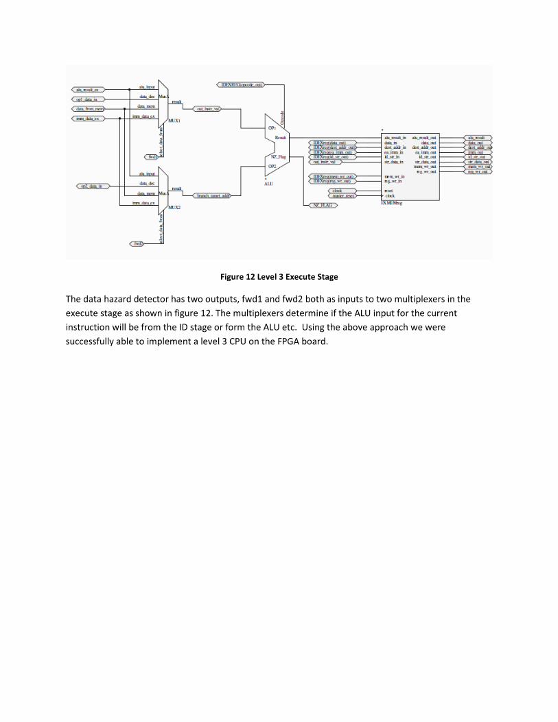
Figure 12 Level 3 Execute Stage
The data hazard detector has two outputs, fwd1 and fwd2 both as inputs to two multiplexers in the
execute stage as shown in figure 12. The multiplexers determine if the ALU input for the current
instruction will be from the ID stage or form the ALU etc. Using the above approach we were
successfully able to implement a level 3 CPU on the FPGA board.
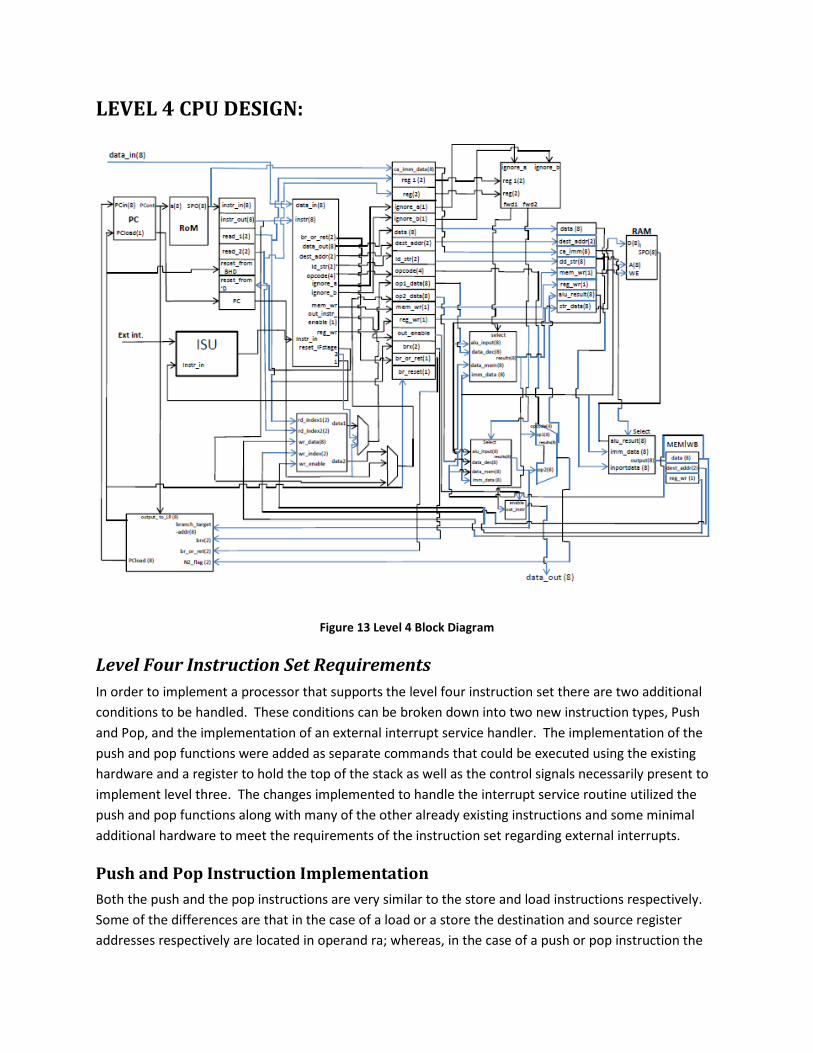
LEVEL 4 CPU DESIGN:
Figure 13 Level 4 Block Diagram
Level Four Instruction Set Requirements
In order to implement a processor that supports the level four instruction set there are two additional
conditions to be handled. These conditions can be broken down into two new instruction types, Push
and Pop, and the implementation of an external interrupt service handler. The implementation of the
push and pop functions were added as separate commands that could be executed using the existing
hardware and a register to hold the top of the stack as well as the control signals necessarily present to
implement level three. The changes implemented to handle the interrupt service routine utilized the
push and pop functions along with many of the other already existing instructions and some minimal
additional hardware to meet the requirements of the instruction set regarding external interrupts.
Push and Pop Instruction Implementation
Both the push and the pop instructions are very similar to the store and load instructions respectively.
Some of the differences are that in the case of a load or a store the destination and source register
addresses respectively are located in operand ra; whereas, in the case of a push or pop instruction the

source and destination register addresses are located in operand rb. This represented a one of many
minor differences in the VHDL code regarding the push and pop commands compared to the load and
store commands which will be described below. With the exception of this minor difference the load
and store commands were successfully implemented by modifying the instruction decoding case
statement in the decoder module of the decode stage to check the four most significant bits of the
instruction for the push or pop op code of ten. If this is the case an if statement will check whether it is
a push or a pop by checking the operand ra to see if it has the value one or zero. If the value of ra is one
then the instruction is a push, but if the value is zero then the instruction is a pop. In the case where the
instruction is evaluated to be a push, precisely the same set of control parameters are set as in the case
of a store except that the source register address is set to be rb instead of ra. In the case where the
instruction is evaluated to be a pop, precisely the same set of control parameters are set as in the case
of a load except that the destination register address is set to be rb instead of ra.
Some additional hardware is required by the push and pop instructions as well. This additional
hardware facilitates the storage of the address of the top of the stack. It is called the Stack Pointer and
is implemented as a separate process within the decoder module of the decode stage. Whenever a
push instruction is decoded, the destination address in the data memory module is set to the value of
the stack pointer. This is handled by the memory stage in much the same way that a store instruction
would be. The difference being that in the case of a store instruction the destination address in the data
memory module would be found in the instruction memory location preceding the store instruction and
would have to be forwarded from the fetch stage upon decoding a store instruction. In the case of a
push instruction there is no need to forward anything from the fetch stage to retrieve the address from
the instruction memory since the destination of the data being stored is determined by the contents of
the stack pointer register. Thus another fundamental difference between a push and a store is that a
push is only one byte long; whereas, a store instruction is two bytes long. Similarly whenever a pop
instruction is executed, the data memory address is not retrieved from the proceeding byte of
instruction memory but instead it is determined by the current value of the stack pointer.
The initial value of the stack pointer is two hundred and fifty five and it is decremented each time a
value is stored on the stack. The order of the usage of the stack pointer and its decrementation are
important. In the case of a push instruction the value of the stack pointer is first used to determine
where the data value will be stored and then it is decremented. In the case of a pop instruction the
value of the stack pointer is decremented and then it is used as the source address of the data value
being read from the data memory and stored in the register file. The implementation of this slight
difference in order of operations is implemented by using an intermediate value which represents the
previous and next value of the stack pointer in order to have the correct location with which to store or
load data to and from data memory. The VHDL code regarding this will simply add or subtract the value
one from the current stack pointer in order to get the correct value since it is known that the stack
pointer will not be incremented or decremented by any values other than one. Since the stack pointer is
in a separate process from the decoding process within the decoder module of the decode stage,
control signals internal to the decoder are used to signal the stack pointer to decrement or increment.
At the end of each clock cycle the stack pointer will be decremented or incremented according to the

value of the stack pointer control signals. The value used as a source or destination address within data
memory is determined by the previously set value of the stack pointer. Thus in the case of a pop the
value used as an address must be decremented by one since the source address of the data value being
stored in data memory will always be pointed to by the current value of the stack pointer minus one. In
this way static arithmetic is used to implement the order of operations regarding when the stack pointer
is modified and when it is used as an address.
External Interrupt Implementation
Much of the design decisions involved in level four were hampered by the desire to keep the maximum
clock frequency of the programmed device very high. One way that we knew this could be
accomplished was by reducing the amount of additional hardware, particularly feedback loops, which
would be introduced by the changes required for the processor to implement the level four instruction
set. Thus the goal of this design was to reduce the amount of hardware introduced to the current
design to the bare minimum necessary to implement external interrupts.
Interrupt Service Unit
In order to implement external interrupts there needed to be a way to detect external interrupt stimuli.
For this purpose a new block consisting of a single latch was added to the primary level three design.
The purpose of this block was solely to detect and remember whether the external button associated
with interrupts was pushed. We were unable to determine a way to directly state that the input from
the external interrupt button was to be edge sensitive so it was necessary to implement edge sensitivity
explicitly in VHDL. This was done by appropriately setting and clearing a variable within the Interrupt
Service Unit (ISU). If the external interrupt button was pushed it would cause a variable to be set and
the value of the internal interrupt signal connected directly to the decode stage of the CPU would be set
as well. If the internal variable is set then the ISU is effectively desensitized to external input until it
receives an interrupt clear signal from the decoder. Upon receiving the interrupt clear signal the
internal variable is cleared along with the internal interrupt signal and the ISU is once again sensitive to
external input. The only time the interrupt clear signal is ever set by the decoder is when a return from
interrupt signal is decoded so this particular design does not support nested interrupts. Also, successive
interrupts will be ignored for the duration of the interrupt service routine. Since the button was being
pressed manually and the processor was being cocked at an extremely high frequency this would be
adequate for the purposes described in the instruction set specification.
Decoder State Machine
The primary modification made in order to handle external interrupts was in the decoder its self. The
level three decode logic was based on a single large case statement which would use the op-code to
determine what control signals to set. In order to implement external interrupt functionality it had to
be divided into several states. In two of the states the decoder would interpret instructions gathered
from the fetch state. These two states were known as the normal flow state and the interrupt service
routine state. All other states were dedicated to transitioning between these two states and were

present to facilitate the issuing of special instructions which would manipulate already present control
signals as well as other control and data signals added for the purpose of implementing level four.
There are thirty one states aside from normal flow and executing interrupt service routine that were
used to enable the smooth transition from normal code execution to interrupt service routine execution
and back again. The large number of states was intended to reduce the amount of additional hardware
necessary and thus keep the clock frequency low once the CPU was complete and fully implementing
the level four instruction set. Many of these states were added to facilitate the completion of tasks that
would necessarily involve more than one stage of the CPU in order to complete a task that future tasks
were dependant on. This was only used when the data hazard detector of level three could not handle
the problem it’s self due to the fact that it was not intended for said purpose.
Once an interrupt is received, signified by the interrupt signal being set by the ISU, the decoder will first
check to see if there as been a branch within the last two instructions. If there has been a branch within
the last two instructions then it will continue in the normal flow mode of execution until this condition is
no longer met. Once there are no branches within the two most recently decoded instructions the
decoder will transition from the normal flow state to the sequence of states which will eventually lead
to the executing interrupt service routine (ISR) state. The first state along the way to executing the ISR is
present in order to avoid data hazards which are not handled by the data hazard detector (DHD) and it is
appropriately named the wait for write back state. This state also contributes to lengthening the
amount of time that the state of the CPU has to settle before the various other transitions which can
effect the link register and N and Z flags. Immediately following this state one clock cycle later are the
four states which push the contents of the register file onto the stack. This was not required in the
specification provided but it did facilitate the desired functionality and also introduced additional
functionality which could be useful to the end user since there code will no longer need to store the
contents of the register file explicitly. The reason these four registers are pushed onto the stack is that
the register file is used during the restoration of the decoder to its original state of normal program
flow. If these registers were not stored to the stack and then retrieved from the stack the register file
would not maintain integrity through the process of executing an interrupt and thus the interrupt
service routine would modify the vales of the register file and interrupt the desired functionality of the
end user’s program. The storing of values to the register file was determined to require less additional
hardware and was thus favourable according to our previously decided mandate of maintaining the
minimum clock period possible. It might have been possible to push the values of the register file as
they were found at the end of the interrupt thus removing the unwanted functionality of automatically
maintained register file integrity. This would involve using the stack in a non-typical way since the
values would have to be pushed over top of the other values such as link register, PC, and N and Z flags.
Following that the retrieval of those three values would involve referencing locations on the stack that
were not at the top of the stack. If those values were popped off of the stack prior to the storage of the
register file on the stack it would introduce complications wherein the register file values would be
overwritten by the PC link register and N and Z flags. For these reason the register file is pushed to the
stack at this time in the ISR initiation sequence. Following the storage of the register file onto the stack
the C is pushed to the stack. In order to do this there were two additional pieces of hardware added.

One was a data path for the PC to be output to the decoder through the IF/ID pipeline register. This
additional hardware was used later on as well for the retrieval of the link register in a complex sequence
discussed later in this document. It was also necessary to add multiplexers to the two read outputs of
the register file. This allowed the portion of the ID/EX pipeline register that was formerly being
populated with the output of the register file to instead be populated with the PC. This would be used
in junction with a push command to place the PC onto the stack later on at the memory stage of the
pipeline. Following the previously described push PC state there was a push N and Z state which
facilitated the storage of the N and Z flag. This state required the addition of a arithmetic command to
be interpreted by the ALU. During the push N and Z state a special push N and Z instruction would be
issued to the ALU and memory stages. This instruction has the control signals associated with the push
instruction but upon receipt by the ALU the result output from the ALU will be set to sex zeros followed
by the N and Z flags stored in the least significant bits of the result byte. After that point it would carry
on down the pipeline to be stored as would any other piece of data in a push instruction. The next four
states in the sequence facilitate the storage of the link register. The first of these four states is the
extract link register state which issues the control signals associated with an unconditional branch. This
causes the contents of the link register to replace the PC which will then be gated through the
aforementioned multiplexer to be stored in the data memory module in the final of the four states in
this sequence. The two states present in the middle of this sequence of four allow for the propagation
of the link register contents through its path from the link register to the PC through the IF/ID stage to
the decoder at which time it can be stored using the push instruction. This is one of the greatest
contributions to the mandate of reduced added hardware mentioned previously. Following this there
are six states required to read the contents of instruction memory at address two and place that value in
the program counter. First there is a state which initiates a branch to static location two in instruction
memory. Then two NOP states are required to allow the PC to be loaded and the contents of memory at
that location to be propagated to the IF/ID pipeline register for use by the decoder. At this pint an
additional multiplexer is added to the output of the register file so that the byte of the ID/EX pipeline
register can be populated directly by what would normally be interpreted as data but is now interpreted
as an address to branch to. The fourth of these six states is present to allow for an unconditional branch
to be executed thus setting the PC to the correct address for the execution of the ISR. The remaining
two states facilitate the time it takes for the unconditional branch to be completed so that the decoder
can return to the decoding state within the ISR mentioned previously called executing ISR.
Upon decoding a return instruction the decoder will exit the executing ISR state and enter the pop link
register state followed by the pop N and Z and pop PC states in that order. These three states issue
commands appropriate to their name and retrieve the three values from the stack in the exact reverse
order that they were pushed onto the stack. The instructions issued in these states do not put the
values back in their appropriate spot but rather place them in the register file to be moved from there to
their final destination. This is to reduce the added hardware as per the aforementioned mandate of
minimizing the clock period. The following three states are utilized to set the link register back to it’s
former value. First a branch is issued to the address determined by the former contents of the link
register which was just popped from the stack prior. Then there is a wait state to allow the branch to be
executed so that the proper PC value will be loaded into the PC. At the third of the three states when

the appropriate PC value is in the PC the control signal pattern of a subroutine branch will be set. This is
so that the link register is loaded with the value of the PC which was loaded in the first of the three
states with the former value of the link register when it was originally stored on the stack upon entering
the ISR. Now that the link register is restored a special instruction can be issued to the ALU to load the
N and Z flags with the proper value. When the ALU receives this special instruction it will transfer the
two least significant bits of the input byte to the N and Z flags in exactly the way they were originally
stored. Once the link register and N and Z flags are restored a branch is issued to restore the PC to its
former value. There is some arithmetic done on the PC when it s first stored to make sure that the PC
value stored is offset by the exact amount that will allow it to iterate through instruction memory a
certain number of times without being in the execution state. The fetched instructions will be ignored
but this will ensure that the PC points to the correct address in instruction memory once execution in
the normal flow state resumes. As the PC iterates to the correct location the former contents of the
register file are restored through a sequence of four pop instructions issued in their own special states.
The pop instructions for each register are issued in the reverse order they were stored to ensure that
the correct values are placed in the correct register. By this time the Program counter has almost
iterated to the correct location and there are only two more wait states before the CPU continues
executing instructions in the normal flow state exactly where it was originally interrupted with no
change to the link register N and Z flags or register file contents. At this time the interrupt clear signal is
asserted and, if the button is no longer being pushed, the ISU becomes sensitive to interrupts again. The
final sequence of states is summarized in Figure 13 below. Certain states are grouped together based on
their primary purpose to simplify the diagram.

Results
Figure 15 Level 1 simulation
• Maximum theoretical frequency of 70.437 MHz
• Critical path between EX/MEM register and MEM/WB register
Figure 14 A summary of the state transitions involved in entering and exiting an interrupt service
routine.

Figure 16 Level 2 stimulation
• Theoretical maximum frequency of 70.437 MHz
• Critical path EX/MEM stage and MEM/WB stage
Figure 17 Level 3 stimulation
• Theoretical maximum frequency of 61.709 MHz
• Critical path between ID, EX and Data Hazard Detector
• Introduced due to data forwarding
• Includes the Data Hazard Detector, Multiplexers which select ALU input, and the ALU
Figure 18 Level 4 stimulation
• Maximum theoretical frequency of 51 MHz.
Table 3 Level 1 Device Utilization Summary
Device Utilization Summary (estimated values) [-]
Logic Utilization Used Available Utilization

Number of Slices 211 7680 2%
Number of Slice Flip Flops 152 15360 0%
Number of 4 input LUTs 354 15360 2%
Number of bonded IOBs 18 221 8%
Number of GCLKs 1 8 12%
Table 4 Level 2 Device Utilization Summary
Device Utilization Summary (estimated values) [-]
Logic Utilization Used Available Utilization
Number of Slices 273 7680 3%
Number of Slice Flip Flops 180 15360 1%
Number of 4 input LUTs 471 15360 3%
Number of bonded IOBs 18 221 8%
Number of GCLKs 1 8 12%
Table 5 Level 3 Device Utilization Summary
Device Utilization Summary [-]
Logic Utilization Used Available Utilization Note(s)
Number of Slice Flip Flops 176 4,704 3%
Number of 4 input LUTs 390 4,704 8%
Number of occupied Slices 306 2,352 13%
Number of Slices containing only related
logic 306 306 100%
Number of Slices containing unrelated logic 0 306 0%
Total Number of 4 input LUTs 520 4,704 11%
Number used as logic 390
Number used as a route-thru 2
Number used for 32x1 RAMs 128
Number of bonded IOBs 17 140 12%

Number of GCLKs 1 4 25%
Number of GCLKIOBs 1 4 25%
Number of RPM macros 1
Table 6 Level 4 Device Utilization Summary
Device Utilization Summary (estimated values) [-]
Logic Utilization Used Available Utilization
Number of Slices 412 7680 5%
Number of Slice Flip Flops 208 15360 1%
Number of 4 input LUTs 785 15360 5%
Number of bonded IOBs 25 221 11%
Number of GCLKs 1 8 12%
Discussion
Pitfalls and Errors:
The major problem we encountered while implementing the 4 levels was avoiding the creation of
latches while using VHDL code to implement the various software components. While implementing the
Level 2 CPUD, the initial design involved a non-clocked ALU. The N and Z flags were taken from the ALU
as an input to the BHD. Although we encountered no problems in the behavioural simulation, the design
would not synthesize on the FPGA board. This was because the N and Z flag output was synthesized as a
latch, the ALU not being clocked. Implementing the ALU as a clocked unit eliminated this error and the
design was successfully implemented on the FPGA board.
While implementing the Level 3 design, we encountered the problem that the branch hazards were no
longer being correctly handled, even though the level 2 code was itself executing correctly. The reason
was that the branch target was itself a potential data hazard. As a result we could no longer take its
value from the ID stage. It value now needed to be taken from the second multiplexer (responsible for
gating the second operand) in the execute stage. A similar problem was encountered for the out
instruction which also needed to be taken from the self same multiplexer in the execute stage.
Design Limitations and Shortcomings:
While dealing with L-type instructions, a NOP is inserted after every such instruction. This introduces
bubbles in the pipeline and reduces the throughput of the system.
The CPU uses static branch not taken technique to detect branch hazards as we said that it performs on
the same level as the static branch taken scheme. However, this technique is only superior the branch
taken scheme if no more than 50% of the branches are taken. If this figure goes past 50%, the branch
taken prediction scheme will perform better.
There are a few design limitations regarding level four. First of all it is not possible to generate an
interrupt while an interrupt is being serviced. This was not required according to the description of the
instruction set provided and would have required additional time to implement since it would require
the ISU to count the number of interrupt button pushes and initiate that many interrupt service routines
one after the other. This may become a problem if the CPU is used for real time applications since it will
miss interrupt signals if they arrive to closer together than the length of the ISR permits them to be
serviced.
Also the push and pop commands do not use separate memory from the data memory block and in the
event that a user does not take into account the size of their stack when designing a specific algorithm it
may be possible to have a stack overflow wherein data is overwritten in the data memory block. This
was also not discussed in the provided description of the instruction set architecture. If time permitted
it may have been useful to implement a command that would let the user access the stack pointer for
reading purposes to be able to track the size of the stack and avoid a stack overflow but as it stands this
is one of the design limitations of the stack of our CPU.
Extra Features
This CPU implements a register file saving and register file restoration sequence at the beginning and
end, respectively, of each interrupt service routine event. This means that the user does not need to
account for saving the contents of the register file whenever entering or leaving an interrupt service
routine. This could avoid certain unfortunate errors wherein the functionality of a program or algorithm
is interrupted by the disruption of the current state of the CPU. In many cases the sudden corruption of
the register file during execution of an algorithm would result in an unrecoverable loss of program
integrity and the results would be erroneous. This is especially important in supercomputing
applications where it is very cumbersome to restart a large calculation from scratch and can take several
days or even weeks to do.
Errors
During the implementation of level four there was a certain intermittent error encountered. This error
was with regard to the external hardware used to trigger an interrupt. There was some logic
surrounding the external interrupt input that would detect when a positive going transition occurred
and trigger an interrupt off of that event alone. This error somewhat improved by switching to a
different board but inevitably there would be the off chance that the button would oscillate, or

“bounce”, from pressed to un pressed, as it was being pressed, in just such a way that the timing of
these events was interpreted as multiple events. This could have been reduced but introducing a
counter to the ISU which would count down after detecting an input and once it reached its terminal
value check the input again so that the input would only be getting checked periodically. This would
avoid the case where the button bounced back to being pressed at exactly the time when the ISR was
finishing and the interrupt input was recently resensitized; however, the nature of the problem is such
that in order to completely avoid the problem of button bounce effects there would have to be external
hardware to completely eliminate it.
There were also several logic errors encountered mostly regarding the logic of implementing a stack;
however, they were solved upon discovery in the functional simulation. An example of such an error
would be the difference in the location of the register source and destination within the push and pop
instructions as compared to the store and load instructions. These errors, and several others which
have already been mentioned, were solved and thus did not produce any symptoms in the final design.
Conclusion
The project was instrumental in helping us learn the details of a pipelined CPU. We were forced to
understand in detail the various hazards encountered while implementing a pipelined CPU. We were
successful in handling all hazards. Dynamic branch prediction would also work better in handling branch
hazards. During the course of this project it became apparent that the implementation of interrupts
within the hardware of a CPU is an extremely complex task with many aspects capable of failure. Based
on the results of this project we have concluded that it may be apt to have an interrupt controller be
less integrated within the CPU. This could be accomplished by having a special sequence of instructions
for extracting and restoring the various values that are required to be saved such as the PC and link
register so that the interrupt process is simplified to a branch and return from a specified memory
location. This would avoid the necessity for a state machine within the decoder having as many states
as was necessary in this particular implementation. Overall the project was a great learning experience.
GLOSSARY
RISC: Reduced Instruction Set Computer
CISC: Complex Instruction Set Computer
ISA: Instruction Set Architecture
FPGA: Field Programmable Gate Array
FF: Flip Flop
CPU: Central Processing Unit

ROM: Read Only Memory
PC: Program Counter
IF: Instruction Fetch
ID: Instruction Decode
EX: Instruction Execute
ALU: Arithmetic and Logical Unit
CPI: Cycles per Instruction
RAM: Random Access Memory
BHD: Branch Hazard Detector
DHD: Data Hazard Detector
LR: Link Register
WAW: Write After Write
WAR: Write After Read
RAW: Read After Write
VHDL: Very High Definition Language
ISR: Interrupt Service Routine
REFERENCES
D. N. Dimopoulos, “Pipelining In Processor” Ceng 450 Course Notes, 2010, pp. 267-268. Available:
www.ece.uvic.ca/~ceng450/.[Accessed: April 2-, 2010].
APPENDICES
Source Code
-----------------------------------------------------------------------------
-----
-- Company:
-- Engineer:
--
-- Create Date: 16:48:21 02/07/2010
-- Design Name:
-- Module Name: ALU - Behavioral
-- Project Name:
-- Target Devices:

-- Tool versions:
-- Description:
--
-- Dependencies:
--
-- Revision:
-- Revision 0.01 - File Created
-- Additional Comments:
--
-----------------------------------------------------------------------------
-----
library IEEE;
use IEEE.STD_LOGIC_1164.ALL;
use IEEE.STD_LOGIC_ARITH.ALL;
--use IEEE.STD_LOGIC_UNSIGNED.ALL;
use WORK.alu_opcodes.all;
use IEEE.STD_LOGIC_SIGNED.ALL;
entity ALU is
port( opcode: IN op_type;
op1: IN std_logic_vector (7 downto 0);
op2: IN std_logic_vector (7 downto 0);
result: OUT std_logic_vector (7 downto 0);
N_Z_flag : OUT std_logic_vector (1 downto 0);
clock : in std_logic);
end ALU;
architecture Behavioral of ALU is
begin
process(opcode, op1, op2) is
variable allzeros : std_logic_vector(7 downto 0) := X"00";
variable temp_result : std_logic_vector(7 downto 0);
variable temp_N_Z_flag : std_logic_vector(1 downto 0);
begin
CASE opcode IS
WHEN add1 => temp_result := op1 + op2;
if(temp_result=allzeros) then--lvl4 Start
temp_N_Z_flag(0) := '1';
else
temp_N_Z_flag(0) := '0';
end if;
temp_N_Z_flag(1) := temp_result(7);
result <= temp_result;--lvl4 End
WHEN sub1 => temp_result := op1 - op2;
if(temp_result=allzeros) then--lvl4 Start
temp_N_Z_flag(0) := '1';
else
temp_N_Z_flag(0) := '0';
end if;
temp_N_Z_flag(1) := temp_result(7);
result <= temp_result;--lvl4 End

WHEN load1 => temp_result := X"00";
result <= temp_result;
WHEN store1 =>temp_result := op1;
result <= temp_result;
WHEN loadimm1 => temp_result := X"00";
result <= temp_result;
WHEN nand1 => temp_result := op1 nand op2;
if(temp_result=allzeros) then--lvl4 Start
temp_N_Z_flag(0) := '1';
else
temp_N_Z_flag(0) := '0';
end if;
temp_N_Z_flag(1) := temp_result(7);--lvl4 End
result <= temp_result;
WHEN mov1 => temp_result := op2;
result <= temp_result;
WHEN nop => temp_result := X"00";
result <= temp_result;
WHEN shl1 => temp_N_Z_flag := "0" & op1(7);
temp_result := op1;--lvl4 Start
for i in 7 downto 1 loop
temp_result(i) := temp_result(i-1);
end loop;
temp_result(0):='0';--lvl4 End
result <= temp_result;
WHEN shr1 => temp_N_Z_flag := "0" & op1(0);
temp_result := op1;--lvl4 Start
for i in 0 to 6 loop
temp_result(i) := temp_result(i+1);
end loop;
temp_result(7):='0';--lvl4 End
result <= temp_result;
WHEN push_NZ => result(7 downto 2) <= "000000";--lvl4
result(1 downto 0) <= temp_N_Z_flag;--lvl4
WHEN pop_NZ => temp_N_Z_flag := op1( 1 downto 0);
result <= X"00";
WHEN others => result <= X"00";
END CASE;
end process;
--new process added with clock-----------------------------------------
------------
process(clock, opcode, op1, op2) is

variable allzeros : std_logic_vector(7 downto 0) := X"00";
variable temp_result : std_logic_vector(7 downto 0);
--variable temp_shift_var : std_logic_vector(7 downto 0);
begin
--N_Z_flag <= "00";
if(rising_edge(clock)) then
CASE opcode IS
WHEN add1 => temp_result := op1 + op2;
if(temp_result=allzeros) then
N_Z_flag(0) <= '1';
else
N_Z_flag(0) <= '0';
end if;
N_Z_flag(1) <= temp_result(7);
WHEN sub1 => temp_result := op1 - op2;
if(temp_result=allzeros) then
N_Z_flag(0) <= '1';
else
N_Z_flag(0) <= '0';
end if;
N_Z_flag(1) <= temp_result(7);
WHEN load1 => temp_result := X"00";
WHEN store1 =>temp_result := op1;
WHEN loadimm1 => temp_result := X"00";
WHEN nand1 => temp_result := op1 nand op2;
if(temp_result=allzeros) then
N_Z_flag(0) <= '1';
else
N_Z_flag(0) <= '0';
end if;
N_Z_flag(1) <= temp_result(7);
WHEN mov1 => temp_result := op2;
WHEN nop => temp_result := X"00";
WHEN shl1 => N_Z_flag <= "0" & op1(7);
temp_result := op1;
for i in 7 downto 1 loop
temp_result(i) := temp_result(i-1);
end loop;
temp_result(0):='0';
WHEN shr1 => N_Z_flag <= "0" & op1(0);
temp_result := op1;
for i in 0 to 6 loop
temp_result(i) := temp_result(i+1);
end loop;
temp_result(7):='0';
WHEN push_NZ => temp_result := X"00";--lvl4

WHEN pop_NZ => N_Z_flag <= op1( 1 downto 0);
temp_result := X"00";
WHEN others => temp_result := X"00";
END CASE;
end if;
--result <= temp_result;
end process;
end Behavioral;

-----------------------------------------------------------------------------
---
-- Company:
-- Engineer:
--
-- Create Date: 14:18:54 03/27/2010
-- Design Name:
-- Module Name: C:/Documents and
Settings/aarotech/Desktop/vgtemp/cpu450/alu_lvl4_tb.vhd
-- Project Name: cpu450
-- Target Device:
-- Tool versions:
-- Description:
--
-- VHDL Test Bench Created by ISE for module: ALU
--
-- Dependencies:
--
-- Revision:
-- Revision 0.01 - File Created
-- Additional Comments:
--
-- Notes:
-- This testbench has been automatically generated using types std_logic and
-- std_logic_vector for the ports of the unit under test. Xilinx recommends
-- that these types always be used for the top-level I/O of a design in order
-- to guarantee that the testbench will bind correctly to the post-
implementation
-- simulation model.
-----------------------------------------------------------------------------
---
LIBRARY ieee;
USE ieee.std_logic_1164.ALL;
USE ieee.std_logic_unsigned.all;
USE ieee.numeric_std.ALL;
USE WORK.alu_opcodes.ALL;
ENTITY alu_lvl4_tb IS
END alu_lvl4_tb;
ARCHITECTURE behavior OF alu_lvl4_tb IS
-- Component Declaration for the Unit Under Test (UUT)
COMPONENT ALU
PORT(
opcode : IN op_type;
op1 : IN std_logic_vector(7 downto 0);
op2 : IN std_logic_vector(7 downto 0);
result : OUT std_logic_vector(7 downto 0);
N_Z_flag : OUT std_logic_vector(1 downto 0);
clock : IN std_logic
);
END COMPONENT;
--Inputs

signal opcode : op_type;
signal op1 : std_logic_vector(7 downto 0) := (others => '0');
signal op2 : std_logic_vector(7 downto 0) := (others => '0');
signal clock : std_logic := '0';
--Outputs
signal result : std_logic_vector(7 downto 0);
signal N_Z_flag : std_logic_vector(1 downto 0);
-- Clock period definitions
constant clock_period : time := 10ns;
BEGIN
-- Instantiate the Unit Under Test (UUT)
uut: ALU PORT MAP (
opcode => opcode,
op1 => op1,
op2 => op2,
result => result,
N_Z_flag => N_Z_flag,
clock => clock
);
-- Clock process definitions
clock_process :process
begin
clock <= '0';
wait for clock_period/2;
clock <= '1';
wait for clock_period/2;
end process;
-- Stimulus process
stim_proc: process
begin
-- hold reset state for 100ms.
wait for 10ns;
opcode <= add1;
op1 <= X"F9";
op2 <= X"01";
wait for 10ns;
assert result = X"03";
wait for 10ns;
opcode <= add1;
op1 <= X"02";
op2 <= X"02";
wait for 10ns;
assert result = X"04";
wait for 10ns;
opcode <= shl1;
op1 <= X"FE";
op2 <= X"00";
wait for 10ns;

assert result = X"AC";
-- insert stimulus here
wait;
end process;
END;
-----------------------------------------------------------------------------
---
-- Company:
-- Engineer:
--
-- Create Date: 12:22:43 02/18/2010
-- Design Name:
-- Module Name: C:/vgtemp/cpu450/alu_tbw.vhd
-- Project Name: cpu450
-- Target Device:
-- Tool versions:
-- Description:
--
-- VHDL Test Bench Created by ISE for module: ALU
--
-- Dependencies:
--
-- Revision:
-- Revision 0.01 - File Created
-- Additional Comments:
--
-- Notes:
-- This testbench has been automatically generated using types std_logic and
-- std_logic_vector for the ports of the unit under test. Xilinx recommends
-- that these types always be used for the top-level I/O of a design in order
-- to guarantee that the testbench will bind correctly to the post-
implementation
-- simulation model.
-----------------------------------------------------------------------------
---
LIBRARY ieee;
USE ieee.std_logic_1164.ALL;
USE ieee.std_logic_unsigned.all;
USE ieee.numeric_std.ALL;
USE WORK.alu_opcodes.ALL;
ENTITY alu_tbw IS
END alu_tbw;
ARCHITECTURE behavior OF alu_tbw IS
-- Component Declaration for the Unit Under Test (UUT)
COMPONENT ALU
PORT(
opcode : IN op_type;
op1 : IN std_logic_vector(7 downto 0);
op2 : IN std_logic_vector(7 downto 0);
result : OUT std_logic_vector(7 downto 0);
N_Z_flag : OUT std_logic_vector(1 downto 0)
);
END COMPONENT;
--Inputs
signal opcode : op_type := add1;
signal op1 : std_logic_vector(7 downto 0) := (others => '0');

signal op2 : std_logic_vector(7 downto 0) := (others => '0');
--Outputs
signal result : std_logic_vector(7 downto 0);
signal N_Z_flag : std_logic_vector(1 downto 0);
BEGIN
-- Instantiate the Unit Under Test (UUT)
uut: ALU PORT MAP (
opcode => opcode,
op1 => op1,
op2 => op2,
result => result,
N_Z_flag => N_Z_flag
);
-- No clocks detected in port list. Replace clk below with
-- appropriate port name
-- Stimulus process
stim_proc: process
begin
-- hold reset state for 100ms.
wait for 10ns;
opcode <= add1;
op1 <= X"F9";
op2 <= X"01";
wait for 10ns;
assert result = X"03";
wait for 10ns;
opcode <= add1;
op1 <= X"02";
op2 <= X"02";
wait for 10ns;
assert result = X"04";
wait for 10ns;
opcode <= shl1;
op1 <= X"FE";
op2 <= X"00";
wait for 10ns;
assert result = X"AC";
-- insert stimulus here
wait;
end process;
END;

-----------------------------------------------------------------------------
-----
-- Company:
-- Engineer:
--
-- Create Date: 15:34:01 02/24/2010
-- Design Name:
-- Module Name: Branch_Predictor - Behavioral
-- Project Name:
-- Target Devices:
-- Tool versions:
-- Description:
--
-- Dependencies:
--
-- Revision:
-- Revision 0.01 - File Created
-- Additional Comments:
--
-----------------------------------------------------------------------------
-----
library IEEE;
use IEEE.STD_LOGIC_1164.ALL;
use IEEE.STD_LOGIC_ARITH.ALL;
use IEEE.STD_LOGIC_UNSIGNED.ALL;
entity Branch_Predictor is
Port (
br_or_ret : in STD_LOGIC_VECTOR (1 downto 0);
brx : in STD_LOGIC_VECTOR (1 downto 0);
nz_flag : in STD_LOGIC_VECTOR (1 downto 0);
branch_enable : out STD_LOGIC_VECTOR (1 downto 0);
branch_subroutine : out std_logic;
PCload : out std_logic);
end Branch_Predictor;
architecture Behavioral of Branch_Predictor is
begin
process(br_or_ret, brx, nz_flag)
begin
branch_enable<="00";
branch_subroutine <= '0';
PCload <= '0';
if(br_or_ret = "10") then
if(brx="00") then
branch_enable<="10";
PCload <= '1';
elsif (brx="01") then
if(nz_flag="01") then
branch_enable<="10";
PCload <= '1';
end if;
elsif (brx="10") then
if(nz_flag="10") then

branch_enable<="10";
PCload <= '1';
end if;
elsif (brx="11") then
branch_enable<="10";
branch_subroutine <= '1';
PCload <= '1';
else
branch_enable<="00";
branch_subroutine <= '0';
PCload <= '0';
end if;
elsif(br_or_ret = "11") then
PCload <= '1';
branch_enable<="11";
else
branch_enable<="00";
branch_subroutine <= '0';
PCload <= '0';
end if;
end process;
end Behavioral;

-----------------------------------------------------------------------------
-----
-- Company:
-- Engineer:
--
-- Create Date: 10:14:29 02/26/2010
-- Design Name:
-- Module Name: BranchHazardDetector - Behavioral
-- Project Name:
-- Target Devices:
-- Tool versions:
-- Description:
--
-- Dependencies:
--
-- Revision:
-- Revision 0.01 - File Created
-- Additional Comments:
--
-----------------------------------------------------------------------------
-----
library IEEE;
use IEEE.STD_LOGIC_1164.ALL;
use IEEE.STD_LOGIC_ARITH.ALL;
use IEEE.STD_LOGIC_UNSIGNED.ALL;
---- Uncomment the following library declaration if instantiating
---- any Xilinx primitives in this code.
--library UNISIM;
--use UNISIM.VComponents.all;
entity BranchHazardDetector is
Port ( br_or_ret : in STD_LOGIC_VECTOR (1 downto 0);
brx : in STD_LOGIC_VECTOR (1 downto 0);
NZ_flag : in STD_LOGIC_VECTOR (1 downto 0);
branch_target_addr : in STD_LOGIC_VECTOR (7 downto 0);
pc_to_lr : in STD_LOGIC_VECTOR (7 downto 0);
PCin_data : out STD_LOGIC_VECTOR (7 downto 0);
PCload : out STD_LOGIC;
clock : in STD_LOGIC;
reset : in STD_LOGIC);
--test signals
--branch_enable_check : out STD_LOGIC_VECTOR (1 downto
0);
--rb_data_check : out std_logic_vector(7 downto 0);
--input port to check if data hazrd exists
--data_hazard : in std_logic;
--input_br_or_ret : out STD_LOGIC_VECTOR (1 downto 0);
--input_brx : out STD_LOGIC_VECTOR (1 downto 0);
--input_nz_flag : out STD_LOGIC_VECTOR (1 downto 0));
end BranchHazardDetector;
architecture Behavioral of BranchHazardDetector is

--signals between branch predictor and link register
signal branch_enable_bp_to_select_pcdata_from : std_logic_vector (1 downto
0);
signal branch_subroutine_bp_to_enable_LR : std_logic;
--signals between link register and MUX
signal LR_out_to_MUX_lr_data : std_logic_vector (7 downto 0);
--check signals
--signal br_en_chk : std_logic_vector(1 downto 0);
--signal rb_chk : std_logic_vector(7 downto 0);
begin
--PCload <= branch_enable_bp_to_select_pcdata_from(1);
--check signals added
--branch_enable_check <= branch_enable_bp_to_select_pcdata_from;
--rb_data_check <= branch_target_addr;
--input_br_or_ret <= br_or_ret;
--input_brx <= brx;
--input_nz_flag <= NZ_flag;
--end of check signals
branchPredictor: entity work.Branch_Predictor
port map(br_or_ret=>br_or_ret,
brx=>brx,
nz_flag=>NZ_flag,
branch_enable=>branch_enable_bp_to_select_pcdata_from,
branch_subroutine=>branch_subroutine_bp_to_enable_LR,
PCload=>PCload);
--reset=>reset);
--data_hazard=>data_hazard);
LR: entity work.LinkRegister
port map(reset=>reset,
enable=>branch_subroutine_bp_to_enable_LR,
LR_in=>pc_to_lr,
LR_out=>LR_out_to_MUX_lr_data,
clock=>clock);
MUX: entity work.MUX_branch_predictor
port
map(select_pcdata_from=>branch_enable_bp_to_select_pcdata_from,
lr_data=>LR_out_to_MUX_lr_data,
rb_data=>branch_target_addr,
output_addr=>PCin_data);
end Behavioral;

-----------------------------------------------------------------------------
-----
-- Company:
-- Engineer:
--
-- Create Date: 14:48:59 02/15/2010
-- Design Name:
-- Module Name: CPULV1 - Behavioral
-- Project Name:
-- Target Devices:
-- Tool versions:
-- Description:
--
-- Dependencies:
--
-- Revision:
-- Revision 0.01 - File Created
-- Additional Comments:
--
-----------------------------------------------------------------------------
-----
library IEEE;
use IEEE.STD_LOGIC_1164.ALL;
use IEEE.STD_LOGIC_ARITH.ALL;
use IEEE.STD_LOGIC_UNSIGNED.ALL;
use WORK.alu_opcodes.all;
---- Uncomment the following library declaration if instantiating
---- any Xilinx primitives in this code.
--library UNISIM;
--use UNISIM.VComponents.all;
entity CPULV1 is
port( master_clock : in std_logic;
master_reset : in std_logic;
extern_intr : in std_logic;
data_in: in std_logic_vector(7 downto 0);
data_out: out std_logic_vector(7 downto 0);
current_state_out : out decoder_state);
--test_pc_out: out std_logic_vector(7 downto 0);
--br_chk : out std_logic_vector (1 downto 0);
--rb_check : out std_logic_vector(7 downto 0);
--dec_br_or_ret : out std_logic_vector (1 downto 0);
--dec_brx : out std_logic_vector (1 downto 0);
--alu_nzflag : out std_logic_vector (1 downto 0));
end CPULV1;
architecture Behavioral of CPULV1 is
--external signals between IF and ID stages
signal IF_to_ID_ea_imm, IF_to_ID_instr : std_logic_vector(7 downto 0);
signal IF_to_ID_rd_index1, IF_to_ID_rd_index2 : std_logic_vector(1 downto 0);
signal ID_to_IF_reset : std_logic;
signal IF_PCout_toID_PCin : std_logic_vector (7 downto 0); --lvl 4

--external signals between ID and WB stages
signal MEMWB_data_out_to_ID_wr_data_regfile : std_logic_vector(7 downto 0);
signal MEMWB_dest_addr_out_to_ID_wr_index_regfile : std_logic_vector(1 downto
0);
signal MEMWB_reg_wr_out_to_ID_wr_en_regfile : std_logic;
--external signals between ID and EX stages
signal IDEX_ea_imm_out_to_EXMEM_ea_imm : std_logic_vector(7 downto 0);
signal IDEX_op1_data_out_ALU_op1, IDEX_op2_data_out_ALU_op2 :
std_logic_vector(7 downto 0);
signal IDEX_ld_str_out_to_EXMEM_ld_str_in : std_logic_vector(1 downto 0);
signal IDEX_dest_addr_out_to_EXMEM_dest_addr_in : std_logic_vector(1 downto
0);
signal IDEX_opcode_out_ALU_operation : op_type;
signal IDEX_mem_wr_out_to_EXMEM_mem_wr_in, IDEX_reg_wr_out_to_EXMEM_reg_wr_in
: std_logic;
signal IDEX_data_out_to_EXMEM_data_in : std_logic_vector(7 downto 0); --
signal connecting idex and exmem : in port data
--external signals between EX and MEM stages
signal EXMEM_ea_out_to_RAM_addr: std_logic_vector(7 downto 0);
signal EXMEM_str_out_RAM_data_in : std_logic_vector(7 downto 0);
signal EXMEM_mem_wr_out_RAM_wen : std_logic;
signal EXMEM_data_out_to_MEMWB_data_in : std_logic_vector (7 downto 0);
--external signals between EX and WB stages
signal EXMEM_imm_out_to_mux_mem_wb_imm_data: std_logic_vector(7 downto 0);
signal EXMEM_alu_result_out_to_mux_mem_wb : std_logic_vector(7 downto 0);
signal EXMEM_ld_str_out_mux_mem_wb_select : std_logic_vector(1 downto 0);
signal EXMEM_dest_addr_out_to_MEMWB_dest_addr_in : std_logic_vector(1 downto
0);
signal EXMEM_reg_wr_out_to_MEMWB_reg_wr_in : std_logic;
--for data hazard between ex and wb stage
signal MEMWB_data_out_to_EX_mux_data_from_mem : std_logic_vector (7 downto
0);
--external signal between MEM and WB stage
signal RAM_data_out_to_mux_mem_wb : std_logic_vector (7 downto 0);
--external signals between ID stage and outinstr_reg
signal IDEX_out_enable_to_outinstr_reg_enable : std_logic;
--signal IDEX_op1_data_out_temp_to_outinstr_reg_data_ra_in :
std_logic_vector(7 downto 0);
signal EXMEM_out_instr_value_to_outinstr_reg_data_ra_in : std_logic_vector(7
downto 0);
--external signals between ID stage and Branch hazard detector
--signal IDEX_op2_data_out_BHD_branch_target_addr : std_logic_vector (7
downto 0);
signal IDEX_br_or_ret_out_to_BHD_br_ret_out : std_logic_vector (1 downto 0);
signal IDEX_brx_out_BHD_brx : std_logic_vector (1 downto 0);
--external signal between EX stage and Branch hazard detector
signal ALU_NZ_flag_to_BDH_NZ_flag : std_logic_vector (1 downto 0);

signal EX_op2_data_out_BHD_branch_target_addr : std_logic_vector (7 downto
0);
--external signals between IF stage and Branch hazard detector
signal PCload_BHD_to_PCload_PC : std_logic;
signal PCin_data_BHD_to_PCin_PC : std_logic_vector (7 downto 0);
signal PC_output_to_LR_BHD_pc_to_lr : std_logic_vector (7 downto 0);
--external signals between data hazard detector and IF stage
--signal PC_hold_dhd_to_hold_IFstage : std_logic;
--external signals between data hazard detector and ID stage
--signal PC_hold_dhd_to_hold_IDstage : std_logic;
signal IDEX_reg1_to_dhd_reg1 : std_logic_vector (1 downto 0);
signal IDEX_reg2_to_dhd_reg2 : std_logic_vector (1 downto 0);
signal IDEX_ignore_a_to_dhd_ignore_a_dec : std_logic;
signal IDEX_ignore_b_to_dhd_ignore_b_dec : std_logic;
signal IDEX_opcode_out_to_dhd_opcode_dec : op_type;
--external signals between data hazard detector and EX stage
--signal PC_hold_dhd_to_hold_EXstage : std_logic;
signal dhd_fwd_1_to_EX_fwd_1 : std_logic_vector (1 downto 0);
signal dhd_fwd_2_to_EX_fwd_2 : std_logic_vector (1 downto 0);
signal EXMEM_dest_addr_out_to_dhd_dest_addr_ex : std_logic_vector (1 downto
0);
signal EXMEM_reg_wr_out_to_dhd_reg_wr_ex : std_logic;
--signal EXMEM_ld_str_out_to_dhd_opcode_ex : std_logic_vector (1 downto 0);
--external signals between data hazard detector and WB stage
signal MEMWB_reg_wr_out_to_dhd_reg_wr_wb : std_logic;
signal MEMWB_dest_addr_out_to_dhd_reg_wr_wb : std_logic_vector (1 downto 0);
--signal MEMWB_ld_str_to_dhd_opcode_wb : std_logic_vector (1 downto 0);
--external signals feedback from EX stage
signal alu_res_feedback : std_logic_vector (7 downto 0);
signal imm_data_feedback : std_logic_vector (7 downto 0);
--signal clr_in : std_logic;--DAP
--signal extern_intr_to_INTR_IN : std_logic;--DAP
--signal between dhd and bhd
--signal PC_hold_dhd_to_bhd : std_logic;
--temp signal to connect hold to different stages
--signal hold_temp : std_logic;
--signal ISU_intr_out_to_FE_intr_in : std_logic;--DAP
signal ISU_intr_out_to_ID_intr_in : std_logic;--DAP
signal ID_clr_out_to_ISU_clr_in : std_logic;--DAP
begin
--For testing
--test_pc_out <= PC_output_to_LR_BHD_pc_to_lr;
--hold signal to IF, ID and EX stage
-- PC_hold_dhd_to_hold_IFstage <= hold_temp;
-- PC_hold_dhd_to_hold_IDstage <= hold_temp;

-- PC_hold_dhd_to_hold_EXstage <= hold_temp;
-- PC_hold_dhd_to_bhd <= hold_temp;
--signals for feedback from ex stage
alu_res_feedback <= EXMEM_alu_result_out_to_mux_mem_wb;
imm_data_feedback <= EXMEM_imm_out_to_mux_mem_wb_imm_data;
--dest addr from extage to data hazard detector
EXMEM_dest_addr_out_to_dhd_dest_addr_ex <=
EXMEM_dest_addr_out_to_MEMWB_dest_addr_in;
--reg write from ex stage to data hazard detector
EXMEM_reg_wr_out_to_dhd_reg_wr_ex <=
EXMEM_reg_wr_out_to_MEMWB_reg_wr_in;
--ldstr from ex stage to dhd
--EXMEM_ld_str_out_to_dhd_opcode_ex <=
EXMEM_ld_str_out_mux_mem_wb_select;
--signal connecting ouptut data from wb stage to ex stage
MEMWB_data_out_to_EX_mux_data_from_mem <=
MEMWB_data_out_to_ID_wr_data_regfile;
--signal connecting reg write from wb stage to dhd
MEMWB_reg_wr_out_to_dhd_reg_wr_wb <=
MEMWB_reg_wr_out_to_ID_wr_en_regfile;
--signal connecting data fromwb stage to dhd
MEMWB_dest_addr_out_to_dhd_reg_wr_wb <=
MEMWB_dest_addr_out_to_ID_wr_index_regfile;
--signal for out instr
--IDEX_op1_data_out_temp_to_outinstr_reg_data_ra_in <=
IDEX_op1_data_out_ALU_op1;
--branch hazard detection signal
--IDEX_op2_data_out_BHD_branch_target_addr <=
IDEX_op2_data_out_ALU_op2;
IDEX_opcode_out_to_dhd_opcode_dec <= IDEX_opcode_out_ALU_operation;
instruction_fetch: entity work.IFStage
port map(clock=>master_clock,
reset=>ID_to_IF_reset,
async_reset=>master_reset,
IFIDout=>IF_to_ID_instr,
read_index1=>IF_to_ID_rd_index1,
read_index2=>IF_to_ID_rd_index2,
IF_to_ID_ea_imm=>IF_to_ID_ea_imm,
PCin=>PCin_data_BHD_to_PCin_PC,
PCload=>PCload_BHD_to_PCload_PC,
output_to_LR=>PC_output_to_LR_BHD_pc_to_lr,
synch_reset=>PCload_BHD_to_PCload_PC,
PCout=>IF_PCout_toID_PCin); --lvl 4
--data hazard
--hold=>PC_hold_dhd_to_hold_IFstage);

instruction_decode: entity work.IDStage
port map(clock=>master_clock,
reset=>master_reset,
data_in=>data_in,
instr_from_mem=>IF_to_ID_instr,
ea_imm_in=>IF_to_ID_ea_imm,
rd_index1=>IF_to_ID_rd_index1,
rd_index2=>IF_to_ID_rd_index2,
wr_en_regfile=>MEMWB_reg_wr_out_to_ID_wr_en_regfile,
wr_index_regfile=>MEMWB_dest_addr_out_to_ID_wr_index_regfile,
wr_data_regfile=>MEMWB_data_out_to_ID_wr_data_regfile,
reset_IFStage=>ID_to_IF_reset,
ea_imm_out=>IDEX_ea_imm_out_to_EXMEM_ea_imm,
ld_str_out=>IDEX_ld_str_out_to_EXMEM_ld_str_in,
opcode_out=>IDEX_opcode_out_ALU_operation,
dest_addr_out=>IDEX_dest_addr_out_to_EXMEM_dest_addr_in,
op1_data_out=>IDEX_op1_data_out_ALU_op1,
op2_data_out=>IDEX_op2_data_out_ALU_op2,
mem_wr_out=>IDEX_mem_wr_out_to_EXMEM_mem_wr_in,
reg_wr_out=>IDEX_reg_wr_out_to_EXMEM_reg_wr_in,
out_enable=>IDEX_out_enable_to_outinstr_reg_enable,
data_out=>IDEX_data_out_to_EXMEM_data_in,
br_or_ret_out=>IDEX_br_or_ret_out_to_BHD_br_ret_out,
brx_out=>IDEX_brx_out_BHD_brx,
synch_reset=>PCload_BHD_to_PCload_PC,
--data hazard
--hold=>PC_hold_dhd_to_hold_IDstage,
reg1=>IDEX_reg1_to_dhd_reg1,
reg2=>IDEX_reg2_to_dhd_reg2,
ignore_a=>IDEX_ignore_a_to_dhd_ignore_a_dec,
ignore_b=>IDEX_ignore_b_to_dhd_ignore_b_dec,
intr_in => ISU_intr_out_to_ID_intr_in,
intr_clr => ID_clr_out_to_ISU_clr_in,
current_state_out => current_state_out,

PCin => IF_PCout_toID_PCin); --lvl4
instruction_execute: entity work.EXstage
port map(clock=>master_clock,
reset=>master_reset,
ea_imm_in=>IDEX_ea_imm_out_to_EXMEM_ea_imm,
ld_str_in=>IDEX_ld_str_out_to_EXMEM_ld_str_in,
dest_addr_in=>IDEX_dest_addr_out_to_EXMEM_dest_addr_in,
opcode_in=>IDEX_opcode_out_ALU_operation,
op1_data_in=>IDEX_op1_data_out_ALU_op1,
op2_data_in=>IDEX_op2_data_out_ALU_op2,
mem_wr_in=>IDEX_mem_wr_out_to_EXMEM_mem_wr_in,
reg_wr_in=>IDEX_reg_wr_out_to_EXMEM_reg_wr_in,
data_in=>IDEX_data_out_to_EXMEM_data_in,-
-data_in added
data_out=>EXMEM_data_out_to_MEMWB_data_in, --data_out added
ea_out=>EXMEM_ea_out_to_RAM_addr,
imm_out=>EXMEM_imm_out_to_mux_mem_wb_imm_data,
str_data_out=>EXMEM_str_out_RAM_data_in,
mem_wr_out=>EXMEM_mem_wr_out_RAM_wen,
alu_result_out=>EXMEM_alu_result_out_to_mux_mem_wb,
ld_str_out=>EXMEM_ld_str_out_mux_mem_wb_select,
reg_wr_out=>EXMEM_reg_wr_out_to_MEMWB_reg_wr_in,
dest_addr_out=>EXMEM_dest_addr_out_to_MEMWB_dest_addr_in,
NZ_flag=>ALU_NZ_flag_to_BDH_NZ_flag,
--data hazard
--hold => PC_hold_dhd_to_hold_EXstage,
--branch targetaddr now come form the
stage
branch_target_addr=>EX_op2_data_out_BHD_branch_target_addr,
fwd_1 => dhd_fwd_1_to_EX_fwd_1,
fwd_2 => dhd_fwd_2_to_EX_fwd_2,
data_from_mem =>
MEMWB_data_out_to_EX_mux_data_from_mem,
alu_result_ex => alu_res_feedback,
imm_data_ex => imm_data_feedback,
--signal for out intsr
out_instr_value =>
EXMEM_out_instr_value_to_outinstr_reg_data_ra_in);

mem_stage: entity work.MEMstage
port map(clock=>master_clock,
--reset=>master_reset,
mem_addr_in=>EXMEM_ea_out_to_RAM_addr,
mem_data_in=>EXMEM_str_out_RAM_data_in,
wr_en=>EXMEM_mem_wr_out_RAM_wen,
mem_data_out=>RAM_data_out_to_mux_mem_wb);
writeback_stage: entity work.WBStage
port map(clock=>master_clock, reset=>master_reset,
dest_addr_in=>EXMEM_dest_addr_out_to_MEMWB_dest_addr_in,
reg_wr_in=>EXMEM_reg_wr_out_to_MEMWB_reg_wr_in,
select_data_from=>EXMEM_ld_str_out_mux_mem_wb_select,
alu_result=>EXMEM_alu_result_out_to_mux_mem_wb,
mem_data=>RAM_data_out_to_mux_mem_wb,
imm_data=>EXMEM_imm_out_to_mux_mem_wb_imm_data,
data_in_wb=>EXMEM_data_out_to_MEMWB_data_in, --
data_in added
--data_out_wb=>data_out,
data_out=>MEMWB_data_out_to_ID_wr_data_regfile,
dest_addr_out=>MEMWB_dest_addr_out_to_ID_wr_index_regfile,
reg_wr_out=>MEMWB_reg_wr_out_to_ID_wr_en_regfile);
--ld_str_wb=>MEMWB_ld_str_to_dhd_opcode_wb);
out_instr_result: entity work.outinstr_reg
port map(enable=>IDEX_out_enable_to_outinstr_reg_enable,
reset=>master_reset,
clock=>master_clock,
--data_ra_in =>
IDEX_op1_data_out_temp_to_outinstr_reg_data_ra_in,
data_ra_in =>
EXMEM_out_instr_value_to_outinstr_reg_data_ra_in,
data_ra_out=>data_out);
--branch hazard detection for level 2
BHD: entity work.BranchHazardDetector
port map(clock=>master_clock,
reset=>master_reset,
branch_target_addr=>EX_op2_data_out_BHD_branch_target_addr,
br_or_ret=>IDEX_br_or_ret_out_to_BHD_br_ret_out,
brx=>IDEX_brx_out_BHD_brx,
NZ_flag=>ALU_NZ_flag_to_BDH_NZ_flag,
PCload=>PCload_BHD_to_PCload_PC,
PCin_data=>PCin_data_BHD_to_PCin_PC,
pc_to_lr=>PC_output_to_LR_BHD_pc_to_lr);

--branch_enable_check => br_chk,
--rb_data_check => rb_check,
--input_br_or_ret => dec_br_or_ret,
--input_brx => dec_brx,
--input_nz_flag => alu_nzflag);
--data_hazard => PC_hold_dhd_to_bhd);
DHD: entity work.DataHazardDetector
port map(reset => master_reset,
opcode_dec =>
IDEX_opcode_out_to_dhd_opcode_dec,
dest_addr_wb =>
MEMWB_dest_addr_out_to_dhd_reg_wr_wb,
--opcode_wb => MEMWB_ld_str_to_dhd_opcode_wb,
reg_wr_wb => MEMWB_reg_wr_out_to_dhd_reg_wr_wb,
dest_addr_ex =>
EXMEM_dest_addr_out_to_dhd_dest_addr_ex,
--opcode_ex =>
EXMEM_ld_str_out_to_dhd_opcode_ex,
reg_wr_ex => EXMEM_reg_wr_out_to_dhd_reg_wr_ex,
--opcode_id => ,
reg1 => IDEX_reg1_to_dhd_reg1,
reg2 => IDEX_reg2_to_dhd_reg2,
ignore_a_dec =>
IDEX_ignore_a_to_dhd_ignore_a_dec,
ignore_b_dec =>
IDEX_ignore_b_to_dhd_ignore_b_dec,
fwd_1 => dhd_fwd_1_to_EX_fwd_1,
fwd_2 => dhd_fwd_2_to_EX_fwd_2);
--PC_hold => hold_temp);
ISU: entity work.InterruptServiceUnit--DAP
port map(clock => master_clock,
clr_in => ID_clr_out_to_ISU_clr_in,--DAP
intr_out_de => ISU_intr_out_to_ID_intr_in,--DAP
INTR_IN => extern_intr);--DAP
end Behavioral;

-----------------------------------------------------------------------------
-----
-- Company:
-- Engineer:
--
-- Create Date: 08:48:24 03/08/2010
-- Design Name:
-- Module Name: DataHazardDetector - Behavioral
-- Project Name:
-- Target Devices:
-- Tool versions:
-- Description:
--
-- Dependencies:
--
-- Revision:
-- Revision 0.01 - File Created
-- Additional Comments:
--
-----------------------------------------------------------------------------
-----
library IEEE;
use IEEE.STD_LOGIC_1164.ALL;
use IEEE.STD_LOGIC_ARITH.ALL;
use IEEE.STD_LOGIC_UNSIGNED.ALL;
use WORK.alu_opcodes.all;
entity DataHazardDetector is
Port ( reset : in STD_LOGIC;
dest_addr_wb : in STD_LOGIC_VECTOR (1 downto 0);
reg_wr_wb : in STD_LOGIC;
dest_addr_ex : in STD_LOGIC_VECTOR (1 downto 0);
reg_wr_ex : in STD_LOGIC;
opcode_dec : in op_type;
reg1 : in std_logic_vector (1 downto 0);
reg2 : in STD_LOGIC_VECTOR (1 downto 0);
ignore_a_dec : in std_logic;
ignore_b_dec : in std_logic;
fwd_1 : out STD_LOGIC_VECTOR (1 downto 0);
fwd_2 : out STD_LOGIC_VECTOR (1 downto 0));
end DataHazardDetector;
architecture Behavioral of DataHazardDetector is
begin
process(reset, opcode_dec, reg1, reg2, reg_wr_ex, reg_wr_wb,
dest_addr_ex, dest_addr_wb)
begin
if(reset = '1') then
fwd_1 <= "00";
fwd_2 <= "00";
--PC_hold <= '0';

else
fwd_1 <= "00";
fwd_2 <= "00";
--PC_hold <= '0';
--check the ignore signals to see if there si apossible
hazard
if(ignore_a_dec = '0' and ignore_b_dec = '0')then--there is
a possible hazard for both operands
if(reg1 = dest_addr_ex and reg_wr_ex = '1')then
fwd_1 <= "10";
elsif(reg1 = dest_addr_wb and reg_wr_wb = '1')then
fwd_1 <= "01";
else
--dummy1 <= '1';--there is no hazard
end if;
if(reg2 = dest_addr_ex and reg_wr_ex = '1')then
fwd_2 <= "10";
elsif(reg2 = dest_addr_wb and reg_wr_wb = '1')then
fwd_2 <= "01";
else
--dummy2 <= '1';--there is no hazard
end if;
elsif(ignore_a_dec = '0' and ignore_b_dec = '1')then--there
is a hazard possible only with operand ra
if(reg1 = dest_addr_ex and reg_wr_ex = '1')then--
fwd_1 <= "10";
elsif(reg1 = dest_addr_wb and reg_wr_wb = '1')then--
fwd_1 <= "01";
else
--dummy3 <= '1';--there is no hazard
end if;
elsif(ignore_a_dec = '1' and ignore_b_dec = '0')then--there
is a hazard possible only with operand rb
if(reg2 = dest_addr_ex and reg_wr_ex = '1')then
fwd_2 <= "10";
elsif(reg2 = dest_addr_wb and reg_wr_wb = '1')then
fwd_2 <= "01";
else
--dummy4 <= '1';--there is no hazard
end if;
else--if(ignore_b_dec = '1' and ignore_b_dec '1')then
--report "Bad forwarding condition";
--dummy5 <= '1';--there is no hazard concerning the
ex stage
end if;
end if;
end process;
end Behavioral;
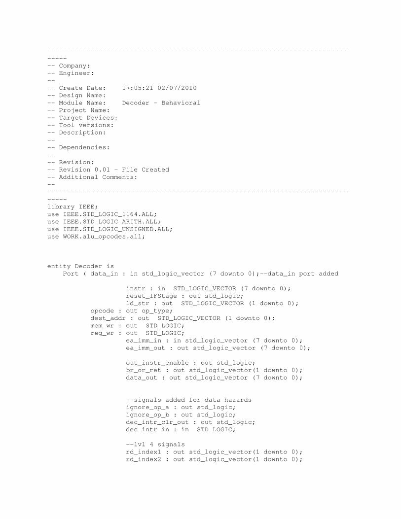
-----------------------------------------------------------------------------
-----
-- Company:
-- Engineer:
--
-- Create Date: 17:05:21 02/07/2010
-- Design Name:
-- Module Name: Decoder - Behavioral
-- Project Name:
-- Target Devices:
-- Tool versions:
-- Description:
--
-- Dependencies:
--
-- Revision:
-- Revision 0.01 - File Created
-- Additional Comments:
--
-----------------------------------------------------------------------------
-----
library IEEE;
use IEEE.STD_LOGIC_1164.ALL;
use IEEE.STD_LOGIC_ARITH.ALL;
use IEEE.STD_LOGIC_UNSIGNED.ALL;
use WORK.alu_opcodes.all;
entity Decoder is
Port ( data_in : in std_logic_vector (7 downto 0);--data_in port added
instr : in STD_LOGIC_VECTOR (7 downto 0);
reset_IFStage : out std_logic;
ld_str : out STD_LOGIC_VECTOR (1 downto 0);
opcode : out op_type;
dest_addr : out STD_LOGIC_VECTOR (1 downto 0);
mem_wr : out STD_LOGIC;
reg_wr : out STD_LOGIC;
ea_imm_in : in std_logic_vector (7 downto 0);
ea_imm_out : out std_logic_vector (7 downto 0);
out_instr_enable : out std_logic;
br_or_ret : out std_logic_vector(1 downto 0);
data_out : out std_logic_vector (7 downto 0);
--signals added for data hazards
ignore_op_a : out std_logic;
ignore_op_b : out std_logic;
dec_intr_clr_out : out std_logic;
dec_intr_in : in STD_LOGIC;
--lvl 4 signals
rd_index1 : out std_logic_vector(1 downto 0);
rd_index2 : out std_logic_vector(1 downto 0);

PC_push : out std_logic_vector (1 downto 0);
interrupt_branch : out std_logic_vector (1 downto 0);
clock : in std_logic;
--test signal
current_state_out : out decoder_state;
--end of test signal
reset : in std_logic);--DAP
end Decoder;
architecture Behavioral of Decoder is
signal current_state : decoder_state;
signal SP : STD_LOGIC_VECTOR (7 downto 0);
signal SP_control : STD_LOGIC_VECTOR (1 downto 0);
signal previous_opcode : std_logic_vector(3 downto 0);
signal exit_isr : std_logic;
begin
process(instr, data_in, ea_imm_in, dec_intr_in, current_state) is
variable operation : STD_LOGIC_VECTOR (3 downto 0) :=x"0";
begin
operation (3 downto 0) := instr (7 downto 4);
dest_addr (1 downto 0) <= instr (3 downto 2);
reg_wr <= '1';
mem_wr <= '0';
ld_str <= "00";
reset_IFStage<='0';
data_out<=data_in;
out_instr_enable<='0';
br_or_ret <= "00";
ignore_op_a <= '1';
ignore_op_b <= '1';
ea_imm_out <= ea_imm_in;
SP_control <= "00";
interrupt_branch <= "00";
rd_index1 <= instr(3 downto 2);
rd_index2 <= instr(1 downto 0);
opcode <= nop;
dec_intr_clr_out <= '0';
case current_state is
when normal_flow => dec_intr_clr_out <= '0';
PC_push <= "00";--lvl4
interrupt_branch <= "00";
case
operation is--OriginalDecoderStartsHere
when "0000" => opcode <= nop;
reg_wr<='0';
ignore_op_a <= '1';

ignore_op_b <='1';
when "0001" => opcode <= load1;
ld_str<="01";
reset_IFStage<='1';
ignore_op_a <= '1';
ignore_op_b <= '1';
when "0010" => opcode <= store1;
ld_str<="00";
reg_wr<='0';
mem_wr<='1';
reset_IFStage<='1';
ignore_op_a <= '0';
ignore_op_b <= '1';
when "0011" => opcode <= loadimm1;
ld_str<="11";
reset_IFStage<='1';
ignore_op_a <= '1';
ignore_op_b <= '1';
when "0100" => opcode <= add1;
ignore_op_a <= '0';
ignore_op_b <= '0';
when "0101" => opcode <= sub1;
ignore_op_a <= '0';

ignore_op_b <= '0';
when "0110" => opcode <= nand1;
ignore_op_a <= '0';
ignore_op_b <= '0';
when "0111" => opcode <= shl1;
ignore_op_a <= '0';
ignore_op_b <= '1';
when "1000" => opcode <= shr1;
ignore_op_a <= '0';
ignore_op_b <= '1';
when "1010" => opcode <= push_pop;
ignore_op_a <= '1';
dest_addr (1 downto 0) <= instr (1 downto 0);
if(instr(3 downto 2) = "01")then--push
ld_str<="00";
ea_imm_out <= SP - 1;
SP_control <= "01";--SP := SP - 1;
mem_wr <= '1';
reg_wr <= '0';
ignore_op_b <= '1';
elsif(instr(3 downto 2) = "00")then--pop
ld_str<="01";
SP_control <= "10";--SP := SP + 1;
ea_imm_out <= SP;

mem_wr <= '0';
reg_wr <= '1';
ignore_op_b <= '0';
else
--ERROR
end if;
when "1011" => opcode <= out1;
out_instr_enable<= '1';
reg_wr<='0';
ignore_op_a <= '0';
ignore_op_b <= '1';
when "1100" => opcode <= in1;
data_out<=data_in;
ld_str<="10";
reg_wr<='1';
ignore_op_a <= '1';
ignore_op_b <= '1';
when "1101" => opcode <= mov1;
ignore_op_a <= '1';
ignore_op_b <= '0';
--signal for level 2 (branch or return)
when "1001" => opcode <=branch1;
br_or_ret <= "10";
reg_wr<='0';
mem_wr<='0';

ignore_op_a <= '1';
ignore_op_b <= '0';
when "1110" => opcode <=return1;
br_or_ret <= "11";
reg_wr<='0';
mem_wr<='0';
ignore_op_a <= '1';
ignore_op_b <= '0';
when others => opcode <=nop;
reg_wr<='0';
mem_wr<='0';
ignore_op_a <= '1';
ignore_op_b <= '1';
end
case;--OriginalDecoderEndsHere
when wait_for_wb => opcode <=nop;
reg_wr<='0';
mem_wr<='0';
ignore_op_a <= '1';
ignore_op_b <= '1';
when push_PC => opcode <= push_pop;
ignore_op_a <= '1';
ld_str<="00";
ea_imm_out <= SP - 1;
SP_control <= "01";--SP := SP - 1;
mem_wr <= '1';
reg_wr <= '0';

ignore_op_b <= '1';
if(previous_opcode = "0011")then
PC_push <= "11";
else
PC_push <= "10";
end
if;
when push_NZ_flags => PC_push <= "00";--this is for
PC_Push!!!!!!!!!!!!
opcode <= push_NZ;
ignore_op_a <= '1';
ld_str<="00";
ea_imm_out <= SP - 1;
SP_control <= "01";--SP := SP - 1;
mem_wr <= '1';
reg_wr <= '0';
ignore_op_b <= '1';
when extract_link_register => opcode <=return1;
br_or_ret <= "11";
reg_wr<='0';
mem_wr<='0';
ignore_op_a <= '1';
ignore_op_b <= '0';
rd_index1 <= "11";-- brx is connected to rd_index1, this initiates an
unconditional return thus loading the ppc with the link register contents
when wait_link_register1 => opcode <= nop;
reg_wr<='0';
ignore_op_a <= '1';
ignore_op_b <='1';
when wait_link_register2 => opcode <= nop;
reg_wr<='0';

ignore_op_a <= '1';
ignore_op_b <='1';
when push_link_register => opcode <= push_pop;
ignore_op_a <= '1';
ld_str<="00";
ea_imm_out <= SP - 1;
SP_control <= "01";--SP := SP - 1;
mem_wr <= '1';
reg_wr <= '0';
ignore_op_b <= '1';
PC_push <= "01";
when push_r0 => opcode <= push_pop;
ld_str<="00";
ea_imm_out <= SP - 1;
SP_control <= "01";--SP := SP - 1;
mem_wr <= '1';
reg_wr <= '0';
ignore_op_b <= '1';
rd_index1 <= "00";
when push_r1 => opcode <= push_pop;
ld_str<="00";
ea_imm_out <= SP - 1;
SP_control <= "01";--SP := SP - 1;
mem_wr <= '1';
reg_wr <= '0';
ignore_op_b <= '1';
rd_index1 <= "01";
when push_r2 => opcode <= push_pop;

ld_str<="00";
ea_imm_out <= SP - 1;
SP_control <= "01";--SP := SP - 1;
mem_wr <= '1';
reg_wr <= '0';
ignore_op_b <= '1';
rd_index1 <= "10";
when push_r3 => opcode <= push_pop;
ld_str<="00";
ea_imm_out <= SP - 1;
SP_control <= "01";--SP := SP - 1;
mem_wr <= '1';
reg_wr <= '0';
ignore_op_b <= '1';
rd_index1 <= "11";
when initiate_isr1 => opcode <= branch1; --this nop
is used to initiate the interrupt branch, later the value of the pc will be
read as the address of the interrupt routine
br_or_ret <= "10";
reg_wr<='0';
mem_wr<='0';
ignore_op_a <= '1';
ignore_op_b <= '0';
rd_index1 <= "11";--branch is unconditional
interrupt_branch <= "01";--the PC will be loaded with the value
"00000001"
when initiate_isr2 => opcode <= nop;
reg_wr<='0';
ignore_op_a <= '1';
ignore_op_b <='1';

when initiate_isr3 => opcode <= nop;
reg_wr<='0';
ignore_op_a <= '1';
ignore_op_b <='1';
when initiate_isr4 => opcode <= branch1; --this nop
is used to initiate the interrupt branch, later the value of the pc will be
read as the address of the interrupt routine
br_or_ret <= "10";
reg_wr<='0';
mem_wr<='0';
ignore_op_a <= '1';
ignore_op_b <= '0';
rd_index1 <= "11";--branch is unconditional
interrupt_branch <= "11";--The PC will be loaded with the value which
is currently in the PC, which was loaded with the contents of instruction
memory 2 cycles prior
when initiate_isr5 => opcode <= nop;
reg_wr<='0';
ignore_op_a <= '1';
ignore_op_b <='1';
when initiate_isr6 => opcode <= nop;
reg_wr<='0';
ignore_op_a <= '1';
ignore_op_b <='1';
when executing_isr => --PC_push <= "00";--lvl4
case
operation is--OriginalDecoderStartsHere
when "0000" => opcode <= nop;
reg_wr<='0';
ignore_op_a <= '1';
ignore_op_b <='1';

when "0001" => opcode <= load1;
ld_str<="01";
reset_IFStage<='1';
ignore_op_a <= '1';
ignore_op_b <= '1';
when "0010" => opcode <= store1;
ld_str<="00";
reg_wr<='0';
mem_wr<='1';
reset_IFStage<='1';
ignore_op_a <= '0';
ignore_op_b <= '1';
when "0011" => opcode <= loadimm1;
ld_str<="11";
reset_IFStage<='1';
ignore_op_a <= '1';
ignore_op_b <= '1';
when "0100" => opcode <= add1;
ignore_op_a <= '0';
ignore_op_b <= '0';
when "0101" => opcode <= sub1;
ignore_op_a <= '0';
ignore_op_b <= '0';

when "0110" => opcode <= nand1;
ignore_op_a <= '0';
ignore_op_b <= '0';
when "0111" => opcode <= shl1;
ignore_op_a <= '0';
ignore_op_b <= '1';
when "1000" => opcode <= shr1;
ignore_op_a <= '0';
ignore_op_b <= '1';
when "1010" => opcode <= push_pop;
ignore_op_a <= '1';
dest_addr (1 downto 0) <= instr (1 downto 0);
if(instr(3 downto 2) = "01")then--push
ld_str<="00";
ea_imm_out <= SP - 1;
SP_control <= "01";--SP := SP - 1;
mem_wr <= '1';
reg_wr <= '0';
ignore_op_b <= '1';
elsif(instr(3 downto 2) = "00")then--pop
ld_str<="01";
SP_control <= "10";--SP := SP + 1;
ea_imm_out <= SP;
mem_wr <= '0';

reg_wr <= '1';
ignore_op_b <= '0';
else
--ERROR
end if;
when "1011" => opcode <= out1;
out_instr_enable<= '1';
reg_wr<='0';
ignore_op_a <= '0';
ignore_op_b <= '1';
when "1100" => opcode <= in1;
data_out<=data_in;
ld_str<="10";
reg_wr<='1';
ignore_op_a <= '1';
ignore_op_b <= '1';
when "1101" => opcode <= mov1;
ignore_op_a <= '1';
ignore_op_b <= '0';
--signal for level 2 (branch or return)
when "1001" => opcode <=branch1;
br_or_ret <= "10";
reg_wr<='0';
mem_wr<='0';
ignore_op_a <= '1';
ignore_op_b <= '0';
when "1110" => opcode <= RTI;
exit_isr <= '1';--dec_intr_clr_out <= '1';--
RETURNING FROM ISR HERE. this is modification from the original decoder
reset_IFStage <= '1';
--br_or_ret <= "11"; --special case of return
not using the link register
reg_wr<='0';
mem_wr<='0';
ignore_op_a <= '1';
ignore_op_b <= '0';--end of mopdifications to
original decoder for exiting isr
when others => opcode <= nop;
reg_wr<='0';
mem_wr<='0';
ignore_op_a <= '1';
ignore_op_b <= '1';
end
case;--OriginalDecoderEndsHere
when pop_r3 => opcode <=
push_pop;
ld_str<="01";
SP_control <= "10";--SP := SP + 1;
ea_imm_out <= SP;
mem_wr <= '0';
reg_wr <= '1';
ignore_op_b <= '0';
dest_addr <= "11";
when pop_r2 => opcode <=
push_pop;
ld_str<="01";
SP_control <= "10";--SP := SP + 1;
ea_imm_out <= SP;
mem_wr <= '0';
reg_wr <= '1';
ignore_op_b <= '0';
dest_addr <= "10";
when pop_r1 => opcode <=
push_pop;
ld_str<="01";
SP_control <= "10";--SP := SP + 1;
ea_imm_out <= SP;
mem_wr <= '0';
reg_wr <= '1';
ignore_op_b <= '0';
dest_addr <= "01";
when pop_r0 => opcode <=
push_pop;
ld_str<="01";
SP_control <= "10";--SP := SP + 1;
ea_imm_out <= SP;
mem_wr <= '0';
reg_wr <= '1';
ignore_op_b <= '0';
dest_addr <= "00";
when pop_link_register => opcode <= push_pop;
ld_str<="01";
SP_control <= "10";--SP := SP + 1;
ea_imm_out <= SP;

mem_wr <= '0';
reg_wr <= '1';
ignore_op_b <= '0';
dest_addr <= "00";--Store link register in R0
when pop_NZ_flags => opcode <= push_pop;
ld_str<="01";
SP_control <= "10";--SP := SP + 1;
ea_imm_out <= SP;
mem_wr <= '0';
reg_wr <= '1';
ignore_op_b <= '0';
dest_addr <= "01";--Store N and Z flags in R1
when pop_PC => opcode <=
push_pop;
ld_str<="01";
SP_control <= "10";--SP := SP + 1;
ea_imm_out <= SP;
mem_wr <= '0';
reg_wr <= '1';
ignore_op_b <= '0';
dest_addr <= "10";--Store the program counter in R2
when set_link_register1 => opcode <=branch1;
br_or_ret <= "10";--PC source is rb (rd_index2)
reg_wr<='0';
mem_wr<='0';
ignore_op_a <= '1';
ignore_op_b <= '0';
rd_index1 <= "11";-- brx is connected to rd_index1, this initiates an
unconditional branch based on the resgister pointed to by rb (rd_index2)

rd_index2 <= "00";--the contents of the PC will be loaded with the
contents of R0
when set_link_register2 => opcode <= nop;
reg_wr<='0';
mem_wr<='0';
ignore_op_a <= '1';
ignore_op_b <= '1';
when set_link_register3 => opcode <=branch1;
br_or_ret <= "10";
reg_wr<='0';
mem_wr<='0';
ignore_op_a <= '1';
ignore_op_b <= '0';
rd_index1 <= "11";-- brx is connected to rd_index1, this initiates an
unconditional SUBROUTINE branch thus loading the link register with PC which
was set to R0 in the previous cycle.
--
interrupt_branch <= "10";
when set_NZ_flags => opcode <= push_NZ;
reg_wr<='0';
mem_wr<='0';
ignore_op_a <= '1';
ignore_op_b <= '1';
rd_index1 <= "01";--the N and z flags are moved from R1 into the NZ
flags of the ALU
when return_from_isr1 => opcode <=branch1;
br_or_ret <= "10";--PC source is rb (rd_index2)
reg_wr<='0';
mem_wr<='0';
ignore_op_a <= '1';
ignore_op_b <= '0';

rd_index1 <= "00";-- brx is connected to rd_index1, this initiates an
unconditional branch based on the resgister pointed to by rb (rd_index2)
rd_index2 <= "10";--the contents of the PC will be loaded with the
contents of R2
--
dec_intr_clr_out <= '1';
when return_from_isr2 => opcode <=nop;
reg_wr<='0';
mem_wr<='0';
ignore_op_a <= '1';
ignore_op_b <= '1';
when return_from_isr3 => opcode <=nop;
exit_isr <= '0';
dec_intr_clr_out <= '1';
reg_wr<='0';
mem_wr<='0';
ignore_op_a <= '1';
ignore_op_b <= '1';
when others => opcode <=nop;
reg_wr<='0';
mem_wr<='0';
ignore_op_a <= '1';
ignore_op_b <= '1';
end case;--DAPEndsHere
--current_state_out <= current_state;
current_state_out <= current_state;
end process;
process(clock, reset, SP_control) is
begin
if(reset = '1')then
SP <= X"FF";
--SP_control <= "00";
else
if(rising_edge(clock))then
if(current_state = normal_flow)then

previous_opcode <= instr(7 downto 4);
end if;
if(SP_control = "01")then
SP <= SP - 1;
elsif(SP_control = "10")then
SP <= SP + 1;
else
SP <= SP;
end if;
end if;
end if;
end process;
process(clock, reset, dec_intr_in) is
begin
if(reset = '1')then
current_state <= normal_flow;
elsif(rising_edge(clock))then
case current_state is--DAPStartsHere
when normal_flow => if((dec_intr_in = '1')
and (previous_opcode /= "1001") and (previous_opcode /= "1110"))then-- and
(instr(7 downto 4) /= "1001") and (instr(7 downto 4) /= "1110"))then
current_state <= wait_for_wb;
end
if;
when wait_for_wb => current_state <=
push_r0;
when push_r0 => current_state <=
push_r1;
when push_r1 => current_state <=
push_r2;
when push_r2 => current_state <=
push_r3;
when push_r3 => current_state <=
push_PC;--push the PC onto the stack
when push_PC => current_state <=
push_NZ_flags;
when push_NZ_flags => current_state <=
extract_link_register;
when extract_link_register => current_state <=
wait_link_register1;--initiate a return instruction to place the link
register in the pc to be read from the pc to be used by the PC_push
instruction
when wait_link_register1 => current_state <=
wait_link_register2;--wait for the pc, containing the former contents of the
link register, to propagate to the decoder
when wait_link_register2 => current_state <=
push_link_register;--wait for the pc, containing the former contents of the
link register, to propagate to the decoder
when push_link_register => current_state <=
initiate_isr1;--push the former contents of the link register, which are
currentl at the PC input to the decoder, onto the stack
when initiate_isr1 => current_state <=
initiate_isr2;--save the return address based on the program counter and
issue a branch instruction into the isr

when initiate_isr2 => current_state <=
initiate_isr3;--save the return address based on the program counter and
issue a branch instruction into the isr
when initiate_isr3 => current_state <=
initiate_isr4;--save the return address based on the program counter and
issue a branch instruction into the isr
when initiate_isr4 => current_state <=
initiate_isr5;--save the return address based on the program counter and
issue a branch instruction into the isr
when initiate_isr5 => current_state <=
initiate_isr6;--save the return address based on the program counter and
issue a branch instruction into the isr
when initiate_isr6 => current_state <=
executing_isr;--save the return address based on the program counter and
issue a branch instruction into the isr
when executing_isr => if(exit_isr = '1')then--
dec_intr_in = '0')then
current_state <= pop_link_register;
end
if;
when pop_link_register => current_state <=
pop_NZ_flags;
when pop_NZ_flags => current_state <=
pop_PC;
when pop_PC => current_state <=
set_link_register1;
when set_link_register1 => current_state <=
set_link_register2;--initiate a branch instruction to place the pre-
interrrupt link register in the pc to be used to load the link register
when set_link_register2 => current_state <=
set_link_register3;--initiate a branch instruction to place the pre-
interrrupt link register in the pc to be used to load the link register
when set_link_register3 => current_state <=
set_NZ_flags;--move the contents of the pc, which now contains the pre-
interrupt contents of the link register, into the link register by issuing a
SUBROUTINE BRANCH
when set_NZ_flags => current_state <=
return_from_isr1;
when return_from_isr1 => current_state <= pop_r3;
when pop_r3 => current_state <=
pop_r2;
when pop_r2 => current_state <=
pop_r1;
when pop_r1 => current_state <=
pop_r0;
when pop_r0 => current_state <=
return_from_isr2;
when return_from_isr2 => current_state <=
return_from_isr3;
when return_from_isr3 => current_state <=
normal_flow;--clr hould be set here
when others => current_state <=
normal_flow;
end case;--DAPEndsHere end process;
end if;
end process;

end Behavioral;

-----------------------------------------------------------------------------
-----
-- Company:
-- Engineer:
--
-- Create Date: 15:02:46 02/12/2010
-- Design Name:
-- Module Name: EXMEMreg - Behavioral
-- Project Name:
-- Target Devices:
-- Tool versions:
-- Description:
--
-- Dependencies:
--
-- Revision:
-- Revision 0.01 - File Created
-- Additional Comments:
--
-----------------------------------------------------------------------------
-----
library IEEE;
use IEEE.STD_LOGIC_1164.ALL;
use IEEE.STD_LOGIC_ARITH.ALL;
use IEEE.STD_LOGIC_UNSIGNED.ALL;
entity EXMEMreg is
Port ( ea_imm_in : in STD_LOGIC_VECTOR (7 downto 0);
ld_str_in : in STD_LOGIC_VECTOR (1 downto 0);
dest_addr_in : in STD_LOGIC_VECTOR (1 downto 0);
str_data_in : in STD_LOGIC_VECTOR (7 downto 0);
alu_result_in : in STD_LOGIC_VECTOR (7 downto 0);
mem_wr_in : in STD_LOGIC;
reg_wr_in : in STD_LOGIC;
clock : in STD_LOGIC;
reset : in STD_LOGIC;
data_in : in STD_LOGIC_VECTOR (7 downto 0);
data_out : out STD_LOGIC_VECTOR (7 downto 0);
ea_imm_out : out STD_LOGIC_VECTOR (7 downto 0);
ld_str_out : out STD_LOGIC_VECTOR (1 downto 0);
dest_addr_out : out STD_LOGIC_VECTOR (1 downto 0);
str_data_out : out STD_LOGIC_VECTOR (7 downto 0);
alu_result_out : out STD_LOGIC_VECTOR (7 downto 0);
mem_wr_out : out STD_LOGIC;
reg_wr_out : out STD_LOGIC);
--signals for data hazard detection
--hold : in std_logic);
end EXMEMreg;
architecture Behavioral of EXMEMreg is
begin
process(clock, reset) is

begin
if(reset='1') then
ea_imm_out <= X"00";
ld_str_out <= "00";
dest_addr_out <= "00";
mem_wr_out <= '0';
reg_wr_out <= '0';
str_data_out <= X"00";
alu_result_out <= X"00";
data_out <= X"00";
elsif(rising_edge(clock)) then
ea_imm_out <= ea_imm_in;
ld_str_out <= ld_str_in;
dest_addr_out <= dest_addr_in;
mem_wr_out <= mem_wr_in;
reg_wr_out <= reg_wr_in;
str_data_out <= str_data_in;
alu_result_out <= alu_result_in;
data_out <= data_in;
end if;
end process;
end Behavioral;

-----------------------------------------------------------------------------
-----
-- Company:
-- Engineer:
--
-- Create Date: 15:20:31 02/12/2010
-- Design Name:
-- Module Name: EXstage - Behavioral
-- Project Name:
-- Target Devices:
-- Tool versions:
-- Description:
--
-- Dependencies:
--
-- Revision:
-- Revision 0.01 - File Created
-- Additional Comments:
--
-----------------------------------------------------------------------------
-----
library IEEE;
use IEEE.STD_LOGIC_1164.ALL;
use IEEE.STD_LOGIC_ARITH.ALL;
use IEEE.STD_LOGIC_UNSIGNED.ALL;
use WORK.alu_opcodes.all;
---- Uncomment the following library declaration if instantiating
---- any Xilinx primitives in this code.
--library UNISIM;
--use UNISIM.VComponents.all;
entity EXstage is
Port ( ea_imm_in : in STD_LOGIC_VECTOR (7 downto 0);
ld_str_in : in STD_LOGIC_VECTOR (1 downto 0);
dest_addr_in : in STD_LOGIC_VECTOR (1 downto 0);
opcode_in : in op_type;
op1_data_in : in STD_LOGIC_VECTOR (7 downto 0);
op2_data_in : in STD_LOGIC_VECTOR (7 downto 0);
mem_wr_in : in STD_LOGIC;
reg_wr_in : in STD_LOGIC;
ea_out : out STD_LOGIC_VECTOR (7 downto 0);
imm_out : out STD_LOGIC_VECTOR (7 downto 0);
str_data_out : out STD_LOGIC_VECTOR (7 downto 0);
mem_wr_out : out STD_LOGIC;
alu_result_out : out STD_LOGIC_VECTOR (7 downto 0);
ld_str_out : out STD_LOGIC_VECTOR (1 downto 0);
reg_wr_out : out STD_LOGIC;
dest_addr_out : out STD_LOGIC_VECTOR (1 downto 0);
data_in : in std_logic_vector (7 downto 0);--data_in
added
data_out : out std_logic_vector (7 downto 0);--data_out
added

NZ_flag : out std_logic_vector(1 downto 0); --
aysnchronous nz flags
--signals for data hazard
fwd_1 : in std_logic_vector (1 downto 0);
fwd_2 : in std_logic_vector (1 downto 0);
--hold : in std_logic;
data_from_mem : in std_logic_vector (7 downto 0);
alu_result_ex :in std_logic_vector (7 downto 0);
imm_data_ex : in std_logic_vector (7 downto 0);
branch_target_addr : out std_logic_vector (7 downto 0);
out_instr_value : out std_logic_vector (7 downto 0);
clock : in STD_LOGIC;
reset : in STD_LOGIC);
--intr_in : in STD_LOGIC);
end EXstage;
architecture Behavioral of EXstage is
signal ALU_out_EXMEM_alu_result_in : std_logic_vector (7 downto 0);
--signal ALU_NZ_Flag : std_logic_vector (1 downto 0);
SIGNAL ea_imm_out_temp: std_logic_vector(7 downto 0);
--signals for data hazard detection
--mux ouput to alu inputs
signal mux1_output_to_ALU_op1 : std_logic_vector(7 downto 0);
signal mux2_output_to_ALU_op2 : std_logic_vector(7 downto 0);
signal mux1_result_to_EXMEM_str_data_in : std_logic_vector (7 downto 0);
--signal alu result to mux inputs
--signal alu_result_to_mux : std_logic_vector(7 downto 0);
--signal immediate data to mux input
--signal imm_data_to_mux : std_logic_vector ( 7 downto 0);
--signal mux1_to_out_instr_value : std_logic_vector (7 downto 0);
begin
ea_out <= ea_imm_out_temp;
imm_out <= ea_imm_out_temp;
branch_target_addr <= mux2_output_to_ALU_op2;
--signal connecting std_dadat_in to mux1 output
mux1_result_to_EXMEM_str_data_in <= mux1_output_to_ALU_op1;
--alu_result_out <= alu_result_to_mux;
--imm_data_to_mux <= ea_imm_out_temp;
out_instr_value <= mux1_output_to_ALU_op1;
simplealu: entity work.ALU

port map(--op1=>op1_data_in,
--op2=>op2_data_in,
op1=>mux1_output_to_ALU_op1,
op2=>mux2_output_to_ALU_op2,
opcode=>opcode_in,
result=>ALU_out_EXMEM_alu_result_in,
N_Z_flag=>NZ_flag,
clock=>clock);
pipeline3: entity work.EXMEMReg
port map(dest_addr_in=>dest_addr_in,
--str_data_in=>op1_data_in,
str_data_in=>mux1_result_to_EXMEM_str_data_in,
alu_result_in=>ALU_out_EXMEM_alu_result_in,
mem_wr_in=>mem_wr_in,
reg_wr_in=>reg_wr_in,
clock=>clock,
reset=>reset,
ea_imm_in=>ea_imm_in,
ld_str_in=>ld_str_in,
data_in=>data_in,
data_out=>data_out,
str_data_out=>str_data_out,
mem_wr_out=>mem_wr_out,
alu_result_out=>alu_result_out,
reg_wr_out=>reg_wr_out,
dest_addr_out=>dest_addr_out,
ea_imm_out=>ea_imm_out_temp,
ld_str_out=>ld_str_out);
--hold=>hold);
MUX1: entity work.MUX_ALU
port map(data_dec=>op1_data_in,
alu_input=>alu_result_ex,
data_mem=>data_from_mem,
imm_data_ex=>imm_data_ex,
select_data_from=>fwd_1,
result=>mux1_output_to_ALU_op1);
MUX2: entity work.MUX_ALU
port map(data_dec=>op2_data_in,
alu_input=>alu_result_ex,
data_mem=>data_from_mem,
imm_data_ex=>imm_data_ex,
select_data_from=>fwd_2,
result=>mux2_output_to_ALU_op2);
end Behavioral;

-----------------------------------------------------------------------------
-----
-- Company:
-- Engineer:
--
-- Create Date: 18:29:33 02/07/2010
-- Design Name:
-- Module Name: IDEXreg - Behavioral
-- Project Name:
-- Target Devices:
-- Tool versions:
-- Description:
--
-- Dependencies:
--
-- Revision:
-- Revision 0.01 - File Created
-- Additional Comments:
--
-----------------------------------------------------------------------------
-----
library IEEE;
use IEEE.STD_LOGIC_1164.ALL;
use IEEE.STD_LOGIC_ARITH.ALL;
use IEEE.STD_LOGIC_UNSIGNED.ALL;
use WORK.alu_opcodes.all;
entity IDEXreg is
Port ( ea_imm_in : in STD_LOGIC_VECTOR (7 downto 0);
ld_str_in : in STD_LOGIC_VECTOR (1 downto 0);
opcode_in : in op_type;
dest_addr_in : in STD_LOGIC_VECTOR (1 downto 0);
mem_wr_in : in STD_LOGIC;
reg_wr_in : in STD_LOGIC;
op1_data_in : in STD_LOGIC_VECTOR (7 downto 0);
op2_data_in : in STD_LOGIC_VECTOR (7 downto 0);
out_instr_enable_in : in std_logic;
ea_imm_out : out STD_LOGIC_VECTOR (7 downto 0);
ld_str_out : out STD_LOGIC_VECTOR (1 downto 0);
opcode_out : out op_type;
dest_addr_out : out STD_LOGIC_VECTOR (1 downto 0);
mem_wr_out : out STD_LOGIC;
reg_wr_out : out STD_LOGIC;
op1_data_out : out STD_LOGIC_VECTOR (7 downto 0);
op2_data_out : out STD_LOGIC_VECTOR (7 downto 0);
out_instr_enable_out : out std_logic;
data_in : in STD_LOGIC_VECTOR (7 downto 0);
data_out : out STD_LOGIC_VECTOR (7 downto 0);
br_or_ret_in : in std_logic_vector (1 downto 0); --signal
from decoder for lvl2
br_or_ret_out : out std_logic_vector (1 downto 0); --
output from IDEX reg
brx_in : in std_logic_vector (1 downto 0); --ra from IF
stage
brx_out : out std_logic_vector (1 downto 0); --ra output
from IDEX reg
--signals for data hazard detection
ignore_a_in : in std_logic;
ignore_b_in : in std_logic;
ignore_a_out : out std_logic;
ignore_b_out : out std_logic;
--hold : in std_logic;
reg1_in : in std_logic_vector (1 downto 0);
reg2_in : in std_logic_vector (1 downto 0);
reg1_out : out std_logic_vector (1 downto 0);
reg2_out : out std_logic_vector (1 downto 0);
clock : in STD_LOGIC;
synch_reset : in std_logic;
reset : in STD_LOGIC);
end IDEXreg;
architecture Behavioral of IDEXreg is
begin
process(clock, reset)
begin
if(reset='1') then
ea_imm_out <= X"00";
ld_str_out <= "00";
opcode_out <= nop;
dest_addr_out <= "00";
mem_wr_out <= '0';
reg_wr_out <= '0';
op1_data_out <= X"00";
op2_data_out <= X"00";
out_instr_enable_out <= '0';
data_out <=X"00";
br_or_ret_out <= "00";
brx_out <= "00";
ignore_a_out <= '0';
ignore_b_out <= '0';
reg1_out <= "00";
reg2_out <= "00";
elsif(rising_edge(clock)) then
if(synch_reset = '1') then
ea_imm_out <= X"00";
ld_str_out <= "00";
opcode_out <= nop;
dest_addr_out <= "00";
mem_wr_out <= '0';
reg_wr_out <= '0';
op1_data_out <= X"00";
op2_data_out <= X"00";

out_instr_enable_out <= '0';
data_out <=X"00";
br_or_ret_out <= "00";
brx_out <= "00";
ignore_a_out <= '0';
ignore_b_out <= '0';
reg1_out <= "00";
reg2_out <= "00";
else
--if(hold = '0') then
ea_imm_out <= ea_imm_in;
ld_str_out <= ld_str_in;
opcode_out <= opcode_in;
dest_addr_out <= dest_addr_in;
mem_wr_out <= mem_wr_in;
reg_wr_out <= reg_wr_in;
op1_data_out <= op1_data_in;
op2_data_out <= op2_data_in;
out_instr_enable_out <= out_instr_enable_in;
data_out <= data_in;
br_or_ret_out <= br_or_ret_in;
brx_out <= brx_in;
ignore_a_out <= ignore_a_in;
ignore_b_out <= ignore_b_in;
reg1_out <= reg1_in;
reg2_out <= reg2_in;
--end if;
end if;
end if;
end process;
end Behavioral;

-----------------------------------------------------------------------------
-----
-- Company:
-- Engineer:
--
-- Create Date: 10:42:34 02/09/2010
-- Design Name:
-- Module Name: IDStage - Behavioral
-- Project Name:
-- Target Devices:
-- Tool versions:
-- Description:
--
-- Dependencies:
--
-- Revision:
-- Revision 0.01 - File Created
-- Additional Comments:
--
-----------------------------------------------------------------------------
-----
library IEEE;
use IEEE.STD_LOGIC_1164.ALL;
use IEEE.STD_LOGIC_ARITH.ALL;
use IEEE.STD_LOGIC_UNSIGNED.ALL;
use WORK.alu_opcodes.all;
---- Uncomment the following library declaration if instantiating
---- any Xilinx primitives in this code.
--library UNISIM;
--use UNISIM.VComponents.all;
entity IDStage is
Port ( clock : in STD_LOGIC;
reset : in STD_LOGIC;
synch_reset : std_logic;
data_in : in std_logic_vector (7 downto 0);--data_in
added
instr_from_mem : in STD_LOGIC_VECTOR (7 downto 0);
rd_index1 : in STD_LOGIC_VECTOR (1 downto 0);
rd_index2 : in STD_LOGIC_VECTOR (1 downto 0);
ea_imm_in : in STD_LOGIC_VECTOR (7 downto 0);
wr_en_regfile : in STD_LOGIC;
wr_index_regfile: in STD_LOGIC_VECTOR (1 downto 0);
wr_data_regfile : in STD_LOGIC_VECTOR (7 downto 0);
intr_in : in STD_LOGIC;--DAP
intr_clr : out STD_LOGIC;--DAP
reset_IFStage : out std_logic;
ea_imm_out : out STD_LOGIC_VECTOR (7 downto 0);
ld_str_out : out STD_LOGIC_VECTOR (1 downto 0);
opcode_out : out op_type;
dest_addr_out : out STD_LOGIC_VECTOR (1 downto 0);

op1_data_out : out STD_LOGIC_VECTOR (7 downto 0);
op2_data_out : out STD_LOGIC_VECTOR (7 downto 0);
mem_wr_out : out STD_LOGIC;
reg_wr_out : out STD_LOGIC;
out_enable : out std_logic; --1st signal for out instr
--out_port_data : out std_logic_vector(7 downto 0); --
2nd signal for out data
--output signal from ID stage for branches
br_or_ret_out : out std_logic_vector (1 downto 0);
brx_out : out std_logic_vector( 1 downto 0);
--signal for data hazard
--hold : in std_logic;
reg1 : out std_logic_vector (1 downto 0);
reg2 : out std_logic_vector (1 downto 0);
ignore_a : out std_logic;
ignore_b : out std_logic;
data_out : out std_logic_vector (7 downto 0);
PCin : in std_logic_vector(7 downto 0);
--test signals
current_state_out : out decoder_state);
--current_state_out : out decoder_state);--data_out added
end IDStage;
architecture Behavioral of IDStage is
signal ld_str_dec_to_IDEX_ld_str_in : STD_LOGIC_VECTOR(1 downto 0);
signal opcode_dec_to_IDEX_opcode_in : op_type;
signal dest_addr_dec_to_IDEX_dest_addr_in : STD_LOGIC_VECTOR (1 downto
0);
signal mem_wr_dec_to_IDEX_mem_wr_in, reg_wr_dec_to_IDEX_mem_wr_in :
STD_LOGIC;
signal rd1_regfile_to_IDEX_op1_data_in, rd2_regfile_to_IDEX_op2_data_in
: STD_LOGIC_VECTOR (7 downto 0);
signal decoder_out_instr_to_IDEX_out_intsr_in : STD_LOGIC;
signal decoder_data_out_to_IDEX_data_out : STD_LOGIC_VECTOR (7 downto
0);
--signal wire connecting decoder to IDEX for branch instruction
signal br_or_ret_dec_to_IDEX_br_or_ret_in : std_logic_vector (1 downto
0);
--signal wires connceting ugnore a and b lines from decoder to IDEX reg
signal ignore_op_a_dec_to_ignore_a_in_IDEX_stage : std_logic;
signal ignore_op_b_dec_to_ignore_b_in_IDEX_stage : std_logic;
signal dec_ea_imm_out_to_IDEX_ea_imm_in: std_logic_vector(7 downto 0);
--signal wire from decoder to select for mux
signal dec_to_mux : std_logic_vector (1 downto 0); --lvl 4
signal dec_to_mux2 : std_logic_vector (1 downto 0); --lvl 4
signal pc_mux_to_IDEX_op1 : std_logic_vector ( 7 downto 0);

signal pc_mux_to_IDEX_op2 : std_logic_vector ( 7 downto 0);
--signal wire from decoder to regfile
signal dec_rd_index1_to_regfile_rd_index1 : std_logic_vector(1 downto
0);
signal dec_rd_index2_to_regfile_rd_index2 : std_logic_vector(1 downto
0);
begin
DECODER: entity work.Decoder
port map(data_in => data_in,
instr=>instr_from_mem,
ld_str=>ld_str_dec_to_IDEX_ld_str_in,
opcode=>opcode_dec_to_IDEX_opcode_in,
dest_addr=>dest_addr_dec_to_IDEX_dest_addr_in,
mem_wr=>mem_wr_dec_to_IDEX_mem_wr_in,
reg_wr=>reg_wr_dec_to_IDEX_mem_wr_in,
reset_IFStage=>reset_IFStage,
br_or_ret=>br_or_ret_dec_to_IDEX_br_or_ret_in, --output port for br
instr in decoder
out_instr_enable=>decoder_out_instr_to_IDEX_out_intsr_in,
data_out=>decoder_data_out_to_IDEX_data_out,
ignore_op_a=>ignore_op_a_dec_to_ignore_a_in_IDEX_stage,
ignore_op_b=>ignore_op_b_dec_to_ignore_b_in_IDEX_stage,
ea_imm_in=>ea_imm_in,
ea_imm_out=>dec_ea_imm_out_to_IDEX_ea_imm_in,
dec_intr_clr_out => intr_clr,--DAP
--PCin=> PCin, --PC input to decoder lvl4
PC_push => dec_to_mux,
interrupt_branch => dec_to_mux2,
dec_intr_in => intr_in,
rd_index1 =>
dec_rd_index1_to_regfile_rd_index1,
rd_index2 =>
dec_rd_index2_to_regfile_rd_index2,
current_state_out => current_state_out,
clock => clock,
reset => reset);--DAP
REG_FILE: entity work.register_file
port map(--rd_index1=>rd_index1,

--rd_index2=>rd_index2,
rd_index1=>dec_rd_index1_to_regfile_rd_index1,
rd_index2=>dec_rd_index2_to_regfile_rd_index2,
clock=>clock,
reset=>reset,
rd_data1=>rd1_regfile_to_IDEX_op1_data_in,
rd_data2=>rd2_regfile_to_IDEX_op2_data_in,
wr_index=>wr_index_regfile,
wr_data=>wr_data_regfile,
wr_enable=>wr_en_regfile);
pipeline2: entity work.IDEXreg
port map(ea_imm_in=>dec_ea_imm_out_to_IDEX_ea_imm_in,
ld_str_in=>ld_str_dec_to_IDEX_ld_str_in,
opcode_in=>opcode_dec_to_IDEX_opcode_in,
dest_addr_in=>dest_addr_dec_to_IDEX_dest_addr_in,
mem_wr_in=>mem_wr_dec_to_IDEX_mem_wr_in,
reg_wr_in=>reg_wr_dec_to_IDEX_mem_wr_in,
--
op1_data_in=>rd1_regfile_to_IDEX_op1_data_in,
op1_data_in => pc_mux_to_IDEX_op1, --lvl
4
op2_data_in => pc_mux_to_IDEX_op2, --lvl
4
--
op2_data_in=>rd2_regfile_to_IDEX_op2_data_in,
clock=>clock,
reset=>reset,
synch_reset=>synch_reset,
ea_imm_out=>ea_imm_out,
ld_str_out=>ld_str_out,
dest_addr_out=>dest_addr_out,
opcode_out=>opcode_out,
op1_data_out=>op1_data_out,
op2_data_out=>op2_data_out,
mem_wr_out=>mem_wr_out,
out_instr_enable_in=>decoder_out_instr_to_IDEX_out_intsr_in,
out_instr_enable_out=>out_enable,
data_in=>decoder_data_out_to_IDEX_data_out,
data_out=>data_out,
br_or_ret_in=>br_or_ret_dec_to_IDEX_br_or_ret_in, --input port for br
instr in IDEX reg

brx_in=>dec_rd_index1_to_regfile_rd_index1, --brx value for lvl2--DAP
br_or_ret_out=>br_or_ret_out,
brx_out=>brx_out,
reg_wr_out=>reg_wr_out,
--hold=>hold,
reg1_in=>dec_rd_index1_to_regfile_rd_index1,
reg2_in=>dec_rd_index2_to_regfile_rd_index2,
ignore_a_in=>ignore_op_a_dec_to_ignore_a_in_IDEX_stage,
ignore_b_in=>ignore_op_b_dec_to_ignore_b_in_IDEX_stage,
reg1_out=>reg1,
reg2_out=>reg2,
ignore_a_out=>ignore_a,
ignore_b_out=>ignore_b);
--out_instr_result: entity
work.outinstr_reg
MUX_for_OP1: entity work.PC_Push_MUX
port map(select_data => dec_to_mux,
data_reg_file =>
rd1_regfile_to_IDEX_op1_data_in,
data_PC_in => PCin,
op1 => pc_mux_to_IDEX_op1);
MUX_for_OP2: entity work.MUX_for_OP2_address_MUX
port map(select_data => dec_to_mux2,
data_PC_in => PCin,
data_in => instr_from_mem,
data_reg_file =>
rd2_regfile_to_IDEX_op2_data_in,
op2 => pc_mux_to_IDEX_op2);
end Behavioral;

-----------------------------------------------------------------------------
-----
-- Company:
-- Engineer:
--
-- Create Date: 14:14:17 02/03/2010
-- Design Name:
-- Module Name: IFIDreg - Behavioral
-- Project Name:
-- Target Devices:
-- Tool versions:
-- Description:
--
-- Dependencies:
--
-- Revision:
-- Revision 0.01 - File Created
-- Additional Comments:
--
-----------------------------------------------------------------------------
-----
library IEEE;
use IEEE.STD_LOGIC_1164.ALL;
use IEEE.STD_LOGIC_ARITH.ALL;
use IEEE.STD_LOGIC_UNSIGNED.ALL;
entity IFIDreg is
port(instr_in : IN std_logic_vector(7 downto 0);
clock : IN std_logic;
reset : IN std_logic;
reset_for_branch : IN std_logic;
async_reset : IN std_logic;
instr_out : OUT std_logic_vector(7 downto 0);
read1 : OUT std_logic_vector(1 downto 0);
read2 : OUT std_logic_vector(1 downto 0);
PCin : in std_logic_vector(7 downto 0);
PCout : out std_logic_vector(7 downto 0));
end entity IFIDreg;
architecture Behavioral of IFIDreg is
begin
process(clock, async_reset)
begin
if(async_reset='1') then
instr_out <= "00000000";
read1<="00";
read2<="00";
PCout<=X"00";
elsif (rising_edge(clock)) then
if(reset = '1') then --reset for loadimm instr
instr_out <= "00000000";
read1<="00";
read2<="00";

PCout<=PCin;
elsif(reset_for_branch = '1') then --reset for branch
instr_out <= "00000000";
read1<="00";
read2<="00";
PCout<=X"00";
else
instr_out <= instr_in;
read1 <= instr_in(3 downto 2);
read2 <= instr_in(1 downto 0);
PCout<=PCin;
end if;
end if;
end process;
end Behavioral;

-----------------------------------------------------------------------------
-----
-- Company:
-- Engineer:
--
-- Create Date: 15:36:40 02/03/2010
-- Design Name:
-- Module Name: IFStage - Behavioral
-- Project Name:
-- Target Devices:
-- Tool versions:
-- Description:
--
-- Dependencies:
--
-- Revision:
-- Revision 0.01 - File Created
-- Additional Comments:
--
-----------------------------------------------------------------------------
-----
library IEEE;
use IEEE.STD_LOGIC_1164.ALL;
use IEEE.STD_LOGIC_ARITH.ALL;
use IEEE.STD_LOGIC_UNSIGNED.ALL;
---- Uncomment the following library declaration if instantiating
---- any Xilinx primitives in this code.
--library UNISIM;
--use UNISIM.VComponents.all;
entity IFStage is
port(clock, reset, async_reset, synch_reset: IN std_logic;
IFIDout : out std_logic_vector(7 downto 0);
read_index1 : out std_logic_vector(1 downto 0);
read_index2 : out std_logic_vector(1 downto 0);
--IFPCinput : in std_logic_vector(7 downto 0);
IF_to_ID_ea_imm : out std_logic_vector(7 downto 0);
--signals for lvl2
output_to_LR : out std_logic_vector(7 downto 0);
PCin : in std_logic_vector(7 downto 0); -- input from BHD
PCload : in std_logic;
PCout : out std_logic_vector(7 downto 0)); --output from PC to ID
stage
--intr_in : in std_logic);--DAP
--ports for data hazard
--hold : in std_logic);
end IFStage;
architecture Behavioral of IFStage is
SIGNAL PCtoMEM, MEMtoIFID: std_logic_vector(7 downto 0);
SIGNAL memory_out: std_logic_vector(7 downto 0);

component program_memory
port(a: in std_logic_vector(7 downto 0); spo : out
std_logic_vector(7 downto 0));
end component program_memory;
begin
IF_to_ID_ea_imm <= memory_out;
MEMtoIFID <= memory_out;
output_to_LR <= PCtoMEM;
PC: entity work.program_counter
PORT MAP (clock=>clock,
async_reset=>async_reset,
PCout=>PCtoMEM,
PCin=>PCin,
PCload=>PCload);
--PChold=>hold);
IM: program_memory
PORT MAP (a=>PCtoMEM, spo=>memory_out);
PipeLineRegister1: entity work.IFIDreg
PORT MAP (instr_in=>MEMtoIFID,
instr_out=>IFIDout,
clock=>clock,
reset=>reset,
async_reset=>async_reset,
read1=>read_index1,
read2=>read_index2,
reset_for_branch=>synch_reset,
PCin=>PCtoMEM,--input to pipeline reg1
from PC
PCout=>PCout); --output to ID stage
--hold=>hold);
end architecture Behavioral;

-----------------------------------------------------------------------------
-----
-- Company:
-- Engineer:
--
-- Create Date: 15:23:16 03/18/2010
-- Design Name:
-- Module Name: InterruptServiceUnit - Behavioral
-- Project Name:
-- Target Devices:
-- Tool versions:
-- Description:
--
-- Dependencies:
--
-- Revision:
-- Revision 0.01 - File Created
-- Additional Comments:
--
-----------------------------------------------------------------------------
-----
library IEEE;
use IEEE.STD_LOGIC_1164.ALL;
use IEEE.STD_LOGIC_ARITH.ALL;
use IEEE.STD_LOGIC_UNSIGNED.ALL;
entity InterruptServiceUnit is
Port ( INTR_IN : in STD_LOGIC;
clr_in : in STD_LOGIC;
clock : in STD_LOGIC;
intr_out_de : out STD_LOGIC);
end InterruptServiceUnit;
architecture Behavioral of InterruptServiceUnit is
begin
process(INTR_IN, clr_in, clock)
variable interrupt_out_preliminary_value : STD_LOGIC := '0';
variable release_detected : STD_LOGIC := '0';
begin
if(rising_edge(clock))then
if(INTR_IN = '1' and clr_in = '0' and release_detected = '0')then
release_detected := '1';
interrupt_out_preliminary_value := '1';
elsif(clr_in = '1')then
interrupt_out_preliminary_value := '0';
end if;
if(INTR_IN = '0')then
release_detected := '0';
end if;
intr_out_de <= interrupt_out_preliminary_value;--this is to allow
a default value so that it will simulate. this should be optimized out
end if;
end process;

end Behavioral;

-----------------------------------------------------------------------------
-----
-- Company:
-- Engineer:
--
-- Create Date: 15:23:16 03/18/2010
-- Design Name:
-- Module Name: InterruptServiceUnit - Behavioral
-- Project Name:
-- Target Devices:
-- Tool versions:
-- Description:
--
-- Dependencies:
--
-- Revision:
-- Revision 0.01 - File Created
-- Additional Comments:
--
-----------------------------------------------------------------------------
-----
library IEEE;
use IEEE.STD_LOGIC_1164.ALL;
use IEEE.STD_LOGIC_ARITH.ALL;
use IEEE.STD_LOGIC_UNSIGNED.ALL;
---- Uncomment the following library declaration if instantiating
---- any Xilinx primitives in this code.
--library UNISIM;
--use UNISIM.VComponents.all;
entity InterruptServiceUnit is
Port ( INTR_IN : in STD_LOGIC;
clr_in : in STD_LOGIC;
intr_out_fe : out STD_LOGIC;
intr_out_de : out STD_LOGIC;
intr_out_ex : out STD_LOGIC);
end InterruptServiceUnit;
architecture Behavioral of InterruptServiceUnit is
SIGNAL extern_intr_to_INTR_IN : std_logic;
begin
process(INTR_IN, clr_in)
begin
if(INTR_IN = '1')then
intr_out_fe <= '1';
intr_out_de <= '1';
intr_out_ex <= '1';
elsif(clr_in = '1')then
intr_out_fe <= '0';
intr_out_de <= '0';
intr_out_ex <= '0';
end if;
end process;

end Behavioral;
-----------------------------------------------------------------------------
-----
-- Company:
-- Engineer:
--
-- Create Date: 14:30:54 03/18/2010
-- Design Name:
-- Module Name: ISU - Behavioral
-- Project Name:
-- Target Devices:
-- Tool versions:
-- Description:
--
-- Dependencies:
--
-- Revision:
-- Revision 0.01 - File Created
-- Additional Comments:
--
-----------------------------------------------------------------------------
-----
library IEEE;
use IEEE.STD_LOGIC_1164.ALL;
use IEEE.STD_LOGIC_ARITH.ALL;
use IEEE.STD_LOGIC_UNSIGNED.ALL;
---- Uncomment the following library declaration if instantiating
---- any Xilinx primitives in this code.
--library UNISIM;
--use UNISIM.VComponents.all;
entity ISU is
Port ( INTR_IN : in STD_LOGIC;
clr : in STD_LOGIC;
intr_out : out STD_LOGIC);
end ISU;
architecture Behavioral of ISU is
SIGNAL exter_intr_to_INTR_IN, clr_in: std_logic;
SIGNAL intr_out_to_fetch_decode: std_logic;
begin
process(INTR_IN, clr)
begin
if(INTR_IN = '1')then
intr_out <= '1';
elsif(clr = '1')then
intr_out <= '0';
end if;
end process;
end Behavioral;
-----------------------------------------------------------------------------
-----
-- Company:
-- Engineer:
--
-- Create Date: 15:51:04 02/24/2010
-- Design Name:
-- Module Name: LinkRegister - Behavioral
-- Project Name:
-- Target Devices:
-- Tool versions:
-- Description:
--
-- Dependencies:
--
-- Revision:
-- Revision 0.01 - File Created
-- Additional Comments:
--
-----------------------------------------------------------------------------
-----
library IEEE;
use IEEE.STD_LOGIC_1164.ALL;
use IEEE.STD_LOGIC_ARITH.ALL;
use IEEE.STD_LOGIC_UNSIGNED.ALL;
entity LinkRegister is
Port ( LR_in : in STD_LOGIC_VECTOR (7 downto 0);
clock : in std_logic;
reset : in STD_LOGIC;
enable : in STD_LOGIC;
LR_out : out STD_LOGIC_VECTOR (7 downto 0));
end LinkRegister;
architecture Behavioral of LinkRegister is
begin
process(clock, reset)
begin
if(reset='1') then
LR_out <= X"00";
elsif (rising_edge(clock)) then
if(enable='1') then
LR_out<=LR_in -1;
end if;
end if;
end process;
end Behavioral;

-----------------------------------------------------------------------------
---
-- This file is owned and controlled by Xilinx and must be used
--
-- solely for design, simulation, implementation and creation of
--
-- design files limited to Xilinx devices or technologies. Use
--
-- with non-Xilinx devices or technologies is expressly prohibited
--
-- and immediately terminates your license.
--
--
--
-- XILINX IS PROVIDING THIS DESIGN, CODE, OR INFORMATION "AS IS"
--
-- SOLELY FOR USE IN DEVELOPING PROGRAMS AND SOLUTIONS FOR
--
-- XILINX DEVICES. BY PROVIDING THIS DESIGN, CODE, OR INFORMATION
--
-- AS ONE POSSIBLE IMPLEMENTATION OF THIS FEATURE, APPLICATION
--
-- OR STANDARD, XILINX IS MAKING NO REPRESENTATION THAT THIS
--
-- IMPLEMENTATION IS FREE FROM ANY CLAIMS OF INFRINGEMENT,
--
-- AND YOU ARE RESPONSIBLE FOR OBTAINING ANY RIGHTS YOU MAY REQUIRE
--
-- FOR YOUR IMPLEMENTATION. XILINX EXPRESSLY DISCLAIMS ANY
--
-- WARRANTY WHATSOEVER WITH RESPECT TO THE ADEQUACY OF THE
--
-- IMPLEMENTATION, INCLUDING BUT NOT LIMITED TO ANY WARRANTIES OR
--
-- REPRESENTATIONS THAT THIS IMPLEMENTATION IS FREE FROM CLAIMS OF
--
-- INFRINGEMENT, IMPLIED WARRANTIES OF MERCHANTABILITY AND FITNESS
--
-- FOR A PARTICULAR PURPOSE.
--
--
--
-- Xilinx products are not intended for use in life support
--
-- appliances, devices, or systems. Use in such applications are
--
-- expressly prohibited.
--
--
--
-- (c) Copyright 1995-2007 Xilinx, Inc.
--
-- All rights reserved.
--
-----------------------------------------------------------------------------
---
-- You must compile the wrapper file Memory.vhd when simulating

-- the core, Memory. When compiling the wrapper file, be sure to
-- reference the XilinxCoreLib VHDL simulation library. For detailed
-- instructions, please refer to the "CORE Generator Help".
-- The synthesis directives "translate_off/translate_on" specified
-- below are supported by Xilinx, Mentor Graphics and Synplicity
-- synthesis tools. Ensure they are correct for your synthesis tool(s).
LIBRARY ieee;
USE ieee.std_logic_1164.ALL;
-- synthesis translate_off
Library XilinxCoreLib;
-- synthesis translate_on
ENTITY Memory IS
port (
a: IN std_logic_VECTOR(7 downto 0);
spo: OUT std_logic_VECTOR(7 downto 0));
END Memory;
ARCHITECTURE Memory_a OF Memory IS
-- synthesis translate_off
component wrapped_Memory
port (
a: IN std_logic_VECTOR(7 downto 0);
spo: OUT std_logic_VECTOR(7 downto 0));
end component;
-- Configuration specification
for all : wrapped_Memory use entity
XilinxCoreLib.dist_mem_gen_v3_4(behavioral)
generic map(
c_has_clk => 0,
c_has_qdpo_clk => 0,
c_has_qdpo_ce => 0,
c_has_d => 0,
c_has_spo => 1,
c_read_mif => 1,
c_has_qspo => 0,
c_width => 8,
c_reg_a_d_inputs => 0,
c_has_we => 0,
c_pipeline_stages => 0,
c_has_qdpo_rst => 0,
c_reg_dpra_input => 0,
c_qualify_we => 0,
c_sync_enable => 1,
c_depth => 256,
c_has_qspo_srst => 0,
c_has_qdpo_srst => 0,
c_has_dpra => 0,
c_qce_joined => 0,
c_mem_type => 0,
c_has_i_ce => 0,
c_has_dpo => 0,
c_mem_init_file => "Memory.mif",
c_default_data => "0",
c_has_spra => 0,

c_has_qspo_ce => 0,
c_addr_width => 8,
c_has_qdpo => 0,
c_has_qspo_rst => 0);
-- synthesis translate_on
BEGIN
-- synthesis translate_off
U0 : wrapped_Memory
port map (
a => a,
spo => spo);
-- synthesis translate_on
END Memory_a;

-----------------------------------------------------------------------------
-----
-- Company:
-- Engineer:
--
-- Create Date: 16:26:41 02/12/2010
-- Design Name:
-- Module Name: MEMstage - Behavioral
-- Project Name:
-- Target Devices:
-- Tool versions:
-- Description:
--
-- Dependencies:
--
-- Revision:
-- Revision 0.01 - File Created
-- Additional Comments:
--
-----------------------------------------------------------------------------
-----
library IEEE;
use IEEE.STD_LOGIC_1164.ALL;
use IEEE.STD_LOGIC_ARITH.ALL;
use IEEE.STD_LOGIC_UNSIGNED.ALL;
---- Uncomment the following library declaration if instantiating
---- any Xilinx primitives in this code.
--library UNISIM;
--use UNISIM.VComponents.all;
entity MEMstage is
Port ( mem_addr_in : in STD_LOGIC_VECTOR (7 downto 0);
mem_data_in : in STD_LOGIC_VECTOR (7 downto 0);
wr_en : in STD_LOGIC;
clock : in STD_LOGIC;
--reset : in std_logic;
mem_data_out : out STD_LOGIC_VECTOR (7 downto 0));
end MEMstage;
architecture Behavioral of MEMstage is
component RAM_256_8
port(a, d: in std_logic_vector(7 downto 0);we, clk : std_logic; SPO :
out std_logic_vector(7 downto 0));
end component RAM_256_8;
begin
RAM: RAM_256_8
port map(a=>mem_addr_in,
d=>mem_data_in,
we=>wr_en,
SPO=>mem_data_out,
clk=>clock);
end Behavioral;

-----------------------------------------------------------------------------
-----
-- Company:
-- Engineer:
--
-- Create Date: 17:40:51 03/08/2010
-- Design Name:
-- Module Name: MUX_ALU - Behavioral
-- Project Name:
-- Target Devices:
-- Tool versions:
-- Description:
--
-- Dependencies:
--
-- Revision:
-- Revision 0.01 - File Created
-- Additional Comments:
--
-----------------------------------------------------------------------------
-----
library IEEE;
use IEEE.STD_LOGIC_1164.ALL;
use IEEE.STD_LOGIC_ARITH.ALL;
use IEEE.STD_LOGIC_UNSIGNED.ALL;
entity MUX_ALU is
Port ( data_dec : in STD_LOGIC_VECTOR (7 downto 0);
data_mem : in STD_LOGIC_VECTOR (7 downto 0);
imm_data_ex : in STD_LOGIC_VECTOR (7 downto 0);
alu_input : in STD_LOGIC_VECTOR (7 downto 0);
select_data_from : in STD_LOGIC_VECTOR (1 downto 0);
result : out STD_LOGIC_VECTOR (7 downto 0));
end MUX_ALU;
architecture Behavioral of MUX_ALU is
begin
with select_data_from select
result <= data_dec when "00",
data_mem when "01",
alu_input when "10",
imm_data_ex when "11",
data_dec when others;
end Behavioral;

-----------------------------------------------------------------------------
-----
-- Company:
-- Engineer:
--
-- Create Date: 09:40:59 02/26/2010
-- Design Name:
-- Module Name: MUX_branch_predictor - Behavioral
-- Project Name:
-- Target Devices:
-- Tool versions:
-- Description:
--
-- Dependencies:
--
-- Revision:
-- Revision 0.01 - File Created
-- Additional Comments:
--
-----------------------------------------------------------------------------
-----
library IEEE;
use IEEE.STD_LOGIC_1164.ALL;
use IEEE.STD_LOGIC_ARITH.ALL;
use IEEE.STD_LOGIC_UNSIGNED.ALL;
entity MUX_branch_predictor is
Port ( select_pcdata_from : in STD_LOGIC_VECTOR (1 downto 0);
lr_data : in STD_LOGIC_VECTOR (7 downto 0);
rb_data : in STD_LOGIC_VECTOR (7 downto 0);
output_addr : out STD_LOGIC_VECTOR (7 downto 0));
end MUX_branch_predictor;
architecture Behavioral of MUX_branch_predictor is
begin
with select_pcdata_from select
output_addr <= lr_data when "11",
rb_data when "10",
rb_data when others;
end Behavioral;
-----------------------------------------------------------------------------
-----
-- Company:
-- Engineer:
--
-- Create Date: 16:49:49 03/31/2010
-- Design Name:
-- Module Name: MUX_for_OP2_address_MUX - Behavioral
-- Project Name:
-- Target Devices:
-- Tool versions:
-- Description:
--

-- Dependencies:
--
-- Revision:
-- Revision 0.01 - File Created
-- Additional Comments:
--
-----------------------------------------------------------------------------
-----
library IEEE;
use IEEE.STD_LOGIC_1164.ALL;
use IEEE.STD_LOGIC_ARITH.ALL;
use IEEE.STD_LOGIC_UNSIGNED.ALL;
entity MUX_for_OP2_address_MUX is
Port ( data_reg_file : in STD_LOGIC_VECTOR (7 downto 0);
data_PC_in : in STD_LOGIC_VECTOR (7 downto 0);
data_in : in STD_LOGIC_VECTOR (7 downto 0);
select_data : in STD_LOGIC_VECTOR (1 downto 0);
op2 : out STD_LOGIC_VECTOR (7 downto 0));
end MUX_for_OP2_address_MUX;
architecture Behavioral of MUX_for_OP2_address_MUX is
begin
with select_data select
op2 <= data_reg_file when "00",
"00000001" when "01",
data_PC_in when "10",
data_in when "11",
data_reg_file when others;
end Behavioral;

-----------------------------------------------------------------------------
-----
-- Company:
-- Engineer:
--
-- Create Date: 16:55:25 02/12/2010
-- Design Name:
-- Module Name: MUX_MEM_WB - Behavioral
-- Project Name:
-- Target Devices:
-- Tool versions:
-- Description:
--
-- Dependencies:
--
-- Revision:
-- Revision 0.01 - File Created
-- Additional Comments:
--
-----------------------------------------------------------------------------
-----
library IEEE;
use IEEE.STD_LOGIC_1164.ALL;
use IEEE.STD_LOGIC_ARITH.ALL;
use IEEE.STD_LOGIC_UNSIGNED.ALL;
entity MUX_MEM_WB is
Port ( select_data_from : in STD_LOGIC_VECTOR (1 downto 0);
alu_result : in STD_LOGIC_VECTOR (7 downto 0);
mem_data : in STD_LOGIC_VECTOR (7 downto 0);
imm_data : in STD_LOGIC_VECTOR (7 downto 0);
in_port_data : in STD_LOGIC_VECTOR (7 downto 0);
output : out STD_LOGIC_VECTOR (7 downto 0));
end MUX_MEM_WB;
architecture Behavioral of MUX_MEM_WB is
begin
with select_data_from select
output <= alu_result when "00",
imm_data when "11",
in_port_data when "10",
mem_data when "01",
"--------" when others;
end Behavioral;

-----------------------------------------------------------------------------
-----
-- Company:
-- Engineer:
--
-- Create Date: 14:03:09 02/18/2010
-- Design Name:
-- Module Name: outinstr_reg - Behavioral
-- Project Name:
-- Target Devices:
-- Tool versions:
-- Description:
--
-- Dependencies:
--
-- Revision:
-- Revision 0.01 - File Created
-- Additional Comments:
--
-----------------------------------------------------------------------------
-----
library IEEE;
use IEEE.STD_LOGIC_1164.ALL;
use IEEE.STD_LOGIC_ARITH.ALL;
use IEEE.STD_LOGIC_UNSIGNED.ALL;
entity outinstr_reg is
Port ( enable : in STD_LOGIC;
clock : in std_logic;
reset : in std_logic;
data_ra_in : in STD_LOGIC_VECTOR (7 downto 0);
data_ra_out : out STD_LOGIC_VECTOR (7 downto 0));
end outinstr_reg;
architecture Behavioral of outinstr_reg is
begin
process(clock,enable,reset)
begin
if(reset='1') then
data_ra_out<=X"00";
elsif(rising_edge(clock)) then
if(enable='1') then
data_ra_out<=data_ra_in;
end if;
end if;
end process;
end Behavioral;

-----------------------------------------------------------------------------
-----
-- Company:
-- Engineer:
--
-- Create Date: 12:49:28 03/27/2010
-- Design Name:
-- Module Name: PC_Push_MUX - Behavioral
-- Project Name:
-- Target Devices:
-- Tool versions:
-- Description:
--
-- Dependencies:
--
-- Revision:
-- Revision 0.01 - File Created
-- Additional Comments:
--
-----------------------------------------------------------------------------
-----
library IEEE;
use IEEE.STD_LOGIC_1164.ALL;
use IEEE.STD_LOGIC_ARITH.ALL;
use IEEE.STD_LOGIC_UNSIGNED.ALL;
entity PC_Push_MUX is
Port ( select_data : in STD_LOGIC_VECTOR (1 downto 0);
data_reg_file : in STD_LOGIC_VECTOR (7 downto 0);
data_PC_in : in STD_LOGIC_VECTOR (7 downto 0);
op1 : out STD_LOGIC_VECTOR (7 downto 0));
end PC_Push_MUX;
architecture Behavioral of PC_Push_MUX is
begin
with select_data select
op1 <= data_reg_file when "00",
data_PC_in when "01",
data_PC_in - 9 when "10",
data_PC_in - 10 when "11",
data_reg_file when others;
end Behavioral;

library ieee ;
use ieee.std_logic_1164.all;
use ieee.std_logic_unsigned.all;
----------------------------------------------------
entity program_counter is
generic(n: natural :=8);
port( clock: in std_logic;
async_reset: in std_logic;
PCin: in std_logic_vector(n-1 downto 0);
PCload : in std_logic;
PCout: out std_logic_vector(n-1 downto 0));
end program_counter;
----------------------------------------------------
architecture behavioral of program_counter is
signal Pre_Q: std_logic_vector(n-1 downto 0);
begin
process(clock, async_reset)
begin
if async_reset = '1' then
Pre_Q <= "00000010";
elsif (rising_edge(clock)) then
if(PCload='1') then
Pre_Q <= PCin;
else
Pre_Q <= Pre_Q + 1;
end if;
end if;
end process;
PCout <= Pre_Q;
end behavioral;

-----------------------------------------------------------------------------
---
-- This file is owned and controlled by Xilinx and must be used
--
-- solely for design, simulation, implementation and creation of
--
-- design files limited to Xilinx devices or technologies. Use
--
-- with non-Xilinx devices or technologies is expressly prohibited
--
-- and immediately terminates your license.
--
--
--
-- XILINX IS PROVIDING THIS DESIGN, CODE, OR INFORMATION "AS IS"
--
-- SOLELY FOR USE IN DEVELOPING PROGRAMS AND SOLUTIONS FOR
--
-- XILINX DEVICES. BY PROVIDING THIS DESIGN, CODE, OR INFORMATION
--
-- AS ONE POSSIBLE IMPLEMENTATION OF THIS FEATURE, APPLICATION
--
-- OR STANDARD, XILINX IS MAKING NO REPRESENTATION THAT THIS
--
-- IMPLEMENTATION IS FREE FROM ANY CLAIMS OF INFRINGEMENT,
--
-- AND YOU ARE RESPONSIBLE FOR OBTAINING ANY RIGHTS YOU MAY REQUIRE
--
-- FOR YOUR IMPLEMENTATION. XILINX EXPRESSLY DISCLAIMS ANY
--
-- WARRANTY WHATSOEVER WITH RESPECT TO THE ADEQUACY OF THE
--
-- IMPLEMENTATION, INCLUDING BUT NOT LIMITED TO ANY WARRANTIES OR
--
-- REPRESENTATIONS THAT THIS IMPLEMENTATION IS FREE FROM CLAIMS OF
--
-- INFRINGEMENT, IMPLIED WARRANTIES OF MERCHANTABILITY AND FITNESS
--
-- FOR A PARTICULAR PURPOSE.
--
--
--
-- Xilinx products are not intended for use in life support
--
-- appliances, devices, or systems. Use in such applications are
--
-- expressly prohibited.
--
--
--
-- (c) Copyright 1995-2007 Xilinx, Inc.
--
-- All rights reserved.
--
-----------------------------------------------------------------------------
---
-- You must compile the wrapper file program_memory.vhd when simulating

-- the core, program_memory. When compiling the wrapper file, be sure to
-- reference the XilinxCoreLib VHDL simulation library. For detailed
-- instructions, please refer to the "CORE Generator Help".
-- The synthesis directives "translate_off/translate_on" specified
-- below are supported by Xilinx, Mentor Graphics and Synplicity
-- synthesis tools. Ensure they are correct for your synthesis tool(s).
LIBRARY ieee;
USE ieee.std_logic_1164.ALL;
-- synthesis translate_off
Library XilinxCoreLib;
-- synthesis translate_on
ENTITY program_memory IS
port (
a: IN std_logic_VECTOR(7 downto 0);
spo: OUT std_logic_VECTOR(7 downto 0));
END program_memory;
ARCHITECTURE program_memory_a OF program_memory IS
-- synthesis translate_off
component wrapped_program_memory
port (
a: IN std_logic_VECTOR(7 downto 0);
spo: OUT std_logic_VECTOR(7 downto 0));
end component;
-- Configuration specification
for all : wrapped_program_memory use entity
XilinxCoreLib.dist_mem_gen_v3_4(behavioral)
generic map(
c_has_clk => 0,
c_has_qdpo_clk => 0,
c_has_qdpo_ce => 0,
c_has_d => 0,
c_has_spo => 1,
c_read_mif => 1,
c_has_qspo => 0,
c_width => 8,
c_reg_a_d_inputs => 0,
c_has_we => 0,
c_pipeline_stages => 0,
c_has_qdpo_rst => 0,
c_reg_dpra_input => 0,
c_qualify_we => 0,
c_sync_enable => 1,
c_depth => 256,
c_has_qspo_srst => 0,
c_has_qdpo_srst => 0,
c_has_dpra => 0,
c_qce_joined => 0,
c_mem_type => 0,
c_has_i_ce => 0,
c_has_dpo => 0,
c_mem_init_file => "program_memory.mif",
c_default_data => "0",
c_has_spra => 0,

c_has_qspo_ce => 0,
c_addr_width => 8,
c_has_qdpo => 0,
c_has_qspo_rst => 0);
-- synthesis translate_on
BEGIN
-- synthesis translate_off
U0 : wrapped_program_memory
port map (
a => a,
spo => spo);
-- synthesis translate_on
END program_memory_a;

-----------------------------------------------------------------------------
---
-- This file is owned and controlled by Xilinx and must be used
--
-- solely for design, simulation, implementation and creation of
--
-- design files limited to Xilinx devices or technologies. Use
--
-- with non-Xilinx devices or technologies is expressly prohibited
--
-- and immediately terminates your license.
--
--
--
-- XILINX IS PROVIDING THIS DESIGN, CODE, OR INFORMATION "AS IS"
--
-- SOLELY FOR USE IN DEVELOPING PROGRAMS AND SOLUTIONS FOR
--
-- XILINX DEVICES. BY PROVIDING THIS DESIGN, CODE, OR INFORMATION
--
-- AS ONE POSSIBLE IMPLEMENTATION OF THIS FEATURE, APPLICATION
--
-- OR STANDARD, XILINX IS MAKING NO REPRESENTATION THAT THIS
--
-- IMPLEMENTATION IS FREE FROM ANY CLAIMS OF INFRINGEMENT,
--
-- AND YOU ARE RESPONSIBLE FOR OBTAINING ANY RIGHTS YOU MAY REQUIRE
--
-- FOR YOUR IMPLEMENTATION. XILINX EXPRESSLY DISCLAIMS ANY
--
-- WARRANTY WHATSOEVER WITH RESPECT TO THE ADEQUACY OF THE
--
-- IMPLEMENTATION, INCLUDING BUT NOT LIMITED TO ANY WARRANTIES OR
--
-- REPRESENTATIONS THAT THIS IMPLEMENTATION IS FREE FROM CLAIMS OF
--
-- INFRINGEMENT, IMPLIED WARRANTIES OF MERCHANTABILITY AND FITNESS
--
-- FOR A PARTICULAR PURPOSE.
--
--
--
-- Xilinx products are not intended for use in life support
--
-- appliances, devices, or systems. Use in such applications are
--
-- expressly prohibited.
--
--
--
-- (c) Copyright 1995-2007 Xilinx, Inc.
--
-- All rights reserved.
--
-----------------------------------------------------------------------------
---
-- You must compile the wrapper file RAM_256_8.vhd when simulating

-- the core, RAM_256_8. When compiling the wrapper file, be sure to
-- reference the XilinxCoreLib VHDL simulation library. For detailed
-- instructions, please refer to the "CORE Generator Help".
-- The synthesis directives "translate_off/translate_on" specified
-- below are supported by Xilinx, Mentor Graphics and Synplicity
-- synthesis tools. Ensure they are correct for your synthesis tool(s).
LIBRARY ieee;
USE ieee.std_logic_1164.ALL;
-- synthesis translate_off
Library XilinxCoreLib;
-- synthesis translate_on
ENTITY RAM_256_8 IS
port (
A: IN std_logic_VECTOR(7 downto 0);
CLK: IN std_logic;
D: IN std_logic_VECTOR(7 downto 0);
WE: IN std_logic;
SPO: OUT std_logic_VECTOR(7 downto 0));
END RAM_256_8;
ARCHITECTURE RAM_256_8_a OF RAM_256_8 IS
-- synthesis translate_off
component wrapped_RAM_256_8
port (
A: IN std_logic_VECTOR(7 downto 0);
CLK: IN std_logic;
D: IN std_logic_VECTOR(7 downto 0);
WE: IN std_logic;
SPO: OUT std_logic_VECTOR(7 downto 0));
end component;
-- Configuration specification
for all : wrapped_RAM_256_8 use entity
XilinxCoreLib.C_DIST_MEM_V7_1(behavioral)
generic map(
c_qualify_we => 0,
c_mem_type => 1,
c_has_qdpo_rst => 0,
c_has_qspo => 0,
c_has_qspo_rst => 0,
c_has_dpo => 0,
c_has_qdpo_clk => 0,
c_has_d => 1,
c_qce_joined => 0,
c_width => 8,
c_reg_a_d_inputs => 0,
c_latency => 0,
c_has_spo => 1,
c_has_we => 1,
c_depth => 256,
c_has_i_ce => 0,
c_default_data_radix => 1,
c_default_data => "0",
c_has_dpra => 0,
c_has_clk => 1,

c_enable_rlocs => 1,
c_generate_mif => 1,
c_has_qspo_ce => 0,
c_addr_width => 8,
c_has_qdpo_srst => 0,
c_mux_type => 0,
c_has_spra => 0,
c_has_qdpo => 0,
c_mem_init_file => "RAM_256_8.mif",
c_reg_dpra_input => 0,
c_has_qspo_srst => 0,
c_has_rd_en => 0,
c_read_mif => 1,
c_sync_enable => 0,
c_has_qdpo_ce => 0);
-- synthesis translate_on
BEGIN
-- synthesis translate_off
U0 : wrapped_RAM_256_8
port map (
A => A,
CLK => CLK,
D => D,
WE => WE,
SPO => SPO);
-- synthesis translate_on
END RAM_256_8_a;
library ieee;
use ieee.std_logic_1164.all;
use ieee.std_logic_unsigned.all;
entity register_file is
port(reset : in std_logic;
clock: in std_logic;
--read signals
rd_index1: in std_logic_vector(1 downto 0);
rd_index2: in std_logic_vector(1 downto 0);
rd_data1: out std_logic_vector(7 downto 0);
rd_data2: out std_logic_vector(7 downto 0);
--write signals
wr_index: in std_logic_vector(1 downto 0);
wr_data: in std_logic_vector(7 downto 0);
wr_enable: in std_logic);
end register_file;
architecture behavioural of register_file is
type reg_array is array (integer range 0 to 3) of std_logic_vector(7
downto 0);
--internals signals
signal reg_file : reg_array;

begin
--write operation
process(clock)
begin
if(clock='0' and clock'event) then
if(reset='1') then
for i in 0 to 3 loop
reg_file(i)<= (others => '0');
end loop;
elsif(wr_enable='1')then
case wr_index(1 downto 0) is
when "00" => reg_file(0) <=
wr_data;
when "01" => reg_file(1) <=
wr_data;
when "10" => reg_file(2) <=
wr_data;
when "11" => reg_file(3) <=
wr_data;
when others => NULL;
end case;
end if;
end if;
end process;
--read operation
rd_data1 <= reg_file(0) when(rd_index1="00") else
reg_file(1) when(rd_index1="01") else
reg_file(2) when(rd_index1="10") else reg_file(3);
rd_data2 <= reg_file(0) when(rd_index2="00") else
reg_file(1) when(rd_index2="01") else
reg_file(2) when(rd_index2="10") else reg_file(3);
end behavioural;

-----------------------------------------------------------------------------
-----
-- Company:
-- Engineer:
--
-- Create Date: 10:50:13 02/15/2010
-- Design Name:
-- Module Name: WBStage - Behavioral
-- Project Name:
-- Target Devices:
-- Tool versions:
-- Description:
--
-- Dependencies:
--
-- Revision:
-- Revision 0.01 - File Created
-- Additional Comments:
--
-----------------------------------------------------------------------------
-----
library IEEE;
use IEEE.STD_LOGIC_1164.ALL;
use IEEE.STD_LOGIC_ARITH.ALL;
use IEEE.STD_LOGIC_UNSIGNED.ALL;
---- Uncomment the following library declaration if instantiating
---- any Xilinx primitives in this code.
--library UNISIM;
--use UNISIM.VComponents.all;
entity WBStage is
Port ( dest_addr_in : in STD_LOGIC_VECTOR (1 downto 0);
reg_wr_in : in STD_LOGIC;
select_data_from : in STD_LOGIC_VECTOR (1 downto 0);
alu_result : in STD_LOGIC_VECTOR (7 downto 0);
mem_data : in STD_LOGIC_VECTOR (7 downto 0);
imm_data : in STD_LOGIC_VECTOR (7 downto 0);
data_in_wb : in std_logic_vector (7 downto 0);--data_in
added
--data_out_wb : out std_logic_vector (7 downto 0);--
data_out added
data_out : out STD_LOGIC_VECTOR (7 downto 0);
dest_addr_out : out STD_LOGIC_VECTOR (1 downto 0);
reg_wr_out : out STD_LOGIC;
--ld_str_wb : out std_logic_vector (1 downto 0);
clock : in STD_LOGIC;
reset : in STD_LOGIC);
end WBStage;
architecture Behavioral of WBStage is
signal mux_mem_wb_to_MEM_data_in : std_logic_vector(7 downto 0);

begin
MUX: entity work.MUX_MEM_WB
port map(select_data_from=>select_data_from,
alu_result=>alu_result,
mem_data=>mem_data,
imm_data=>imm_data,
in_port_data=>data_in_wb,
output=>mux_mem_wb_to_MEM_data_in);
pipeline4: entity work.MEMWBreg
port map(dest_addr_in=>dest_addr_in,
reg_wr_in=>reg_wr_in,
data_in=>mux_mem_wb_to_MEM_data_in,
clock=>clock,
reset=>reset,
--data_in_wb=>data_in_wb,
--data_out_wb=>data_out_wb,
data_out=>data_out,
dest_addr_out=>dest_addr_out,
reg_wr_out=>reg_wr_out);
--
ld_str_wb_in=>select_data_from,
--ld_str_wb_out=>ld_str_wb);
end Behavioral;

![Ceng 450 Project. Pinout of Processor Interrupt is optional Processor in_port[7:0] out_port[7:0] clock rst interrupt](https://img.pdfslide.us/doc/110x75/56649edb5503460f94bebacf/ceng-450-project-pinout-of-processor-interrupt-is-optional-processor-inport70.jpg)