Embed Size (px)
Citation preview
Product structure : Assemble production using printed circuit board This product is not design for protection against radioactive rays
1/20 © 2016 ROHM Co., Ltd. All rights reserved. www.rohm.com
2016.10.13 Rev.C
Smart Regulator Series 7 to 26V Input, 1.0A, Fixed Output Voltage
3 terminals DC/DC Regulator BP5293-xx Series
General Description
The BP5293-xx series is one packaged 3terminals Buck type DC/DC Converter built-in all parts of DC/DC converter. High efficiency compared with 3 terminals regulator, and not necessary to heat sink. It’s able to rearrange without redesign PCB, because of pin compatible. The built in input/output capacitors and coil is contribute to compact design. Supplied DC30Vmax output fixed voltage which is 3.3V, 5.0V, 12.0V line up. The output max current is 1A. High efficiency at light load with a SLLMTM. It is most suitable for use in the equipment to reduce the standby power is required.
Key Specifications Input Voltage Range: (BP5293-33):
(BP5293-50): (BP5293-12):
Output Decision Voltage:(BP5293-33): (BP5293-50): (BP5293-12):
Maximum Output Current: Operation Temperature Range:
7~26V7~26V
17~26V3.3V±3%5.0V±2%12V±5%
1A (Max.)
-25~85
Features 1ch Buck DC/DC Converter SLLM
TM control(Simple Light Load Mode)
Efficiency=70%(@WOUT=10mW) Over current protection Short protection Under voltage lockout protection Soft start Not need to externals parts Small Package
Appearance
W: 16.0mm x H: 16.8mm x T: 7.2mm (Max.)
Applications Consumer applications such as Home appliances
etc. Industrial equipment Amusement device
Line up Output Voltage Typ.
Vo(T) Product Name
3.3V BP5293-33
5.0V BP5293-50
12.0V BP5293-12
Typical Application Circuit
Figure.1 Application circuit
BP5293-xx
Series
GND
Fuse
Primary
Supply
etc.
VOUTVIN
Device
VCC
Vo :
3.3/5.0/12.0V
Io 1A (Max.)
2/20
DatasheetBP5293-xx Series
© 2016 ROHM Co., Ltd. All rights reserved. 2016.10.13 Rev.C
www.rohm.com
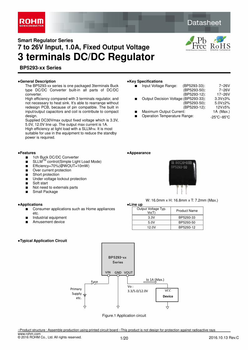
Pin Configuration
Figure.2 Pin Assignment
Pin Descriptions
Block Diagram
Figure.3 Block Diagram
ControllerProtection Circuit
TSDUVLO
OVP
SCP
OCP
1
2
3
Vi
VIN
GND
VOUT
Power Stage
OSC
SLLMTM
SOFT START
Pin No. Symbol Description
1 VIN
Input Power Supply terminal. This is supplied power source for the switching regulator and the controller. Thought An input capacitor is not needed, If made a characteristic better, connect ceramic capacitor recommended 10µF.
2 GND GND terminal
3 VOUT Output terminal. This is output voltage of switching regulator. Thought An input capacitor is not needed, If made a characteristic better, connect ceramic capacitor recommended 10µF.
3/20
DatasheetBP5293-xx Series
© 2016 ROHM Co., Ltd. All rights reserved. 2016.10.13 Rev.C
www.rohm.com
Description of Block
1. Controller
This block is controlled by switching regulator. By monitoring output voltage, controlled transistor switching to be fixed
voltage Vo(T).By internal oscilattor circuit, the transistor is switching 570kHz typ for heavier load.
2. Power Stage
This block is built in two power MOSFETs and a power COIL which are parts for synchronous rectification type switching
regulator. The on resistance of upper power MOSFET is 250mΩ typ and the on resistance of lower power MOSFET is
200mΩ.
3. Protection Circuit
・ UVLO
This circuit is prevented abnormal function for under voltage dropped. When VIN goes under 6.4V typ, the switching
function is stop. The detection voltage is hysterisis 200mV typ.
・ TSD
This circuit is heat protection. When internal temparature goes over 175, the switching function is stop. If the
temparature goes cold 150, the switching function return normal function
・ SCP
This circuit is output short protection. If output voltage goes lower, and keeps among 0.9msec typ, the switching
function is stop. After 14.4msec typ, the swiching fucntion is return normal function.
・ OVP
This circuit is output over voltage protection. If output voltage goes unexpected over voltage, the high-side MOSFET
is OFF. When output voltage goes low which has hysterisis voltage, the switching function return.
・ OCP
If over current, the high-side MOSFET is controled current every 1cycle
Absolute Maximum Ratings (Ta=25°C)
These are the values which must not be exceeded at any time under any application or any test conditions.
Please make design keeping margins accordingly
Parameter Symbol Rating Unit Conditions
Input Voltage VinMAX 30 V VIN terminal
Allowable maximum surface temperature
Tcmax 105 °C Ambient temperature + The module self-heating ≦Tcmax
Operating temperature range Topr -25 ~ +85 °C
Storage temperature range Tstg -40 ~ +85 °C Maximum output current IoMAX 1000 mA
4/20
DatasheetBP5293-xx Series
© 2016 ROHM Co., Ltd. All rights reserved. 2016.10.13 Rev.C
www.rohm.com
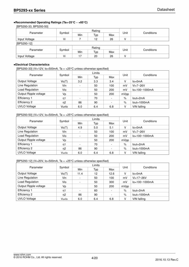
Recommended Operating Ratings (Ta=-25°C ~ +85°C)
[BP5293-33, BP5293-50]
Parameter Symbol Rating
Unit Conditions Min Typ Max
Input Voltage Vi 7 12 26 V
[BP5293-12]
Parameter Symbol Rating
Unit Conditions Min Typ Max
Input Voltage Vi 17 20 26 V
Electrical Characteristics
[BP5293-33] (Vi=12V, Io=500mA, Ta = +25°C unless otherwise specified)
Parameter Symbol Limits
Unit Conditions Min Typ Max
Output Voltage Vo(T) 3.2 3.3 3.4 V Io=0mA
Line Regulation Vln - 50 100 mV Vi=7~26V
Load Regulation Vlo - 50 200 mV Io=100~1000mA
Output Ripple voltage Vp 50 200 mVpp
Efficiency 1 η1 - 70 - % Iout=2mA
Efficiency 2 η2 86 90 - % Iout=1000mA
UVLO Voltage Vuvlo 6.0 6.4 6.8 V VIN falling
[BP5293-50] (Vi=12V, Io=500mA, Ta = +25°C unless otherwise specified)
Parameter Symbol Limits
Unit Conditions Min Typ Max
Output Voltage Vo(T) 4.9 5.0 5.1 V Io=0mA
Line Regulation Vln - 50 100 mV Vi=7~26V
Load Regulation Vlo - 50 200 mV Io=100~1000mA
Output Ripple voltage Vp 50 200 mVpp
Efficiency 1 η1 - 70 - % Iout=2mA
Efficiency 2 η2 86 90 - % Iout=1000mA
UVLO Voltage Vuvlo 6.0 6.4 6.8 V VIN falling
[BP5293-12] (Vi=20V, Io=500mA, Ta = +25°C unless otherwise specified)
Parameter Symbol Limits
Unit Conditions Min Typ Max
Output Voltage Vo(T) 11.4 12 12.6 V Io=0mA
Line Regulation Vln - 50 100 mV Vi=17~26V
Load Regulation Vlo - 50 300 mV Io=100~1000mA
Output Ripple voltage Vp 50 200 mVpp
Efficiency 1 η1 - 60 - % Iout=2mA
Efficiency 2 η2 86 90 - % Iout=1000mA
UVLO Voltage Vuvlo 6.0 6.4 6.8 V VIN falling
5/20
DatasheetBP5293-xx Series
© 2016 ROHM Co., Ltd. All rights reserved. 2016.10.13 Rev.C
www.rohm.com
Description
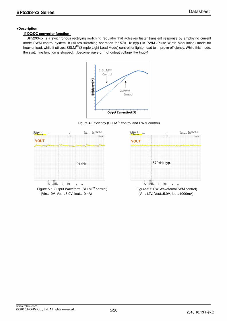
1) DC/DC converter function
BP5293-xx is a synchronous rectifying switching regulator that achieves faster transient response by employing current
mode PWM control system. It utilizes switching operation for 570kHz (typ.) in PWM (Pulse Width Modulation) mode for
heavier load, while it utilizes SSLMTM
(Simple Light Load Mode) control for lighter load to improve efficiency. While this mode,
the switching function is stopped, It become waveform of output voltage like Fig5-1
Figure.4 Efficiency (SLLMTM
control and PWM control)
Figure.5-1 Output Waveform (SLLMTM
control) Figure.5-2 SW Waveform(PWM control)
(Vin=12V, Vout=5.0V, Iout=10mA) (Vin=12V, Vout=5.0V, Iout=1000mA)
570kHz typ.
VOUT VOUT
21kHz
6/20
DatasheetBP5293-xx Series
© 2016 ROHM Co., Ltd. All rights reserved. 2016.10.13 Rev.C
www.rohm.com
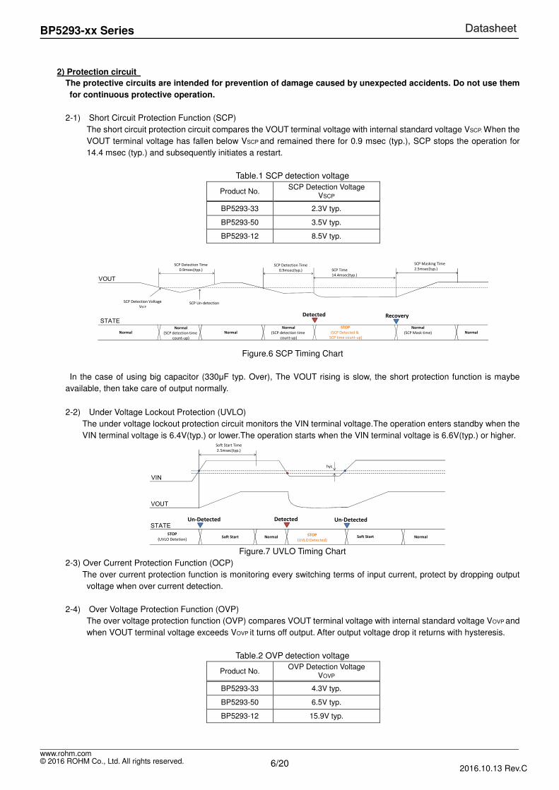
2) Protection circuit
The protective circuits are intended for prevention of damage caused by unexpected accidents. Do not use them
for continuous protective operation.
2-1) Short Circuit Protection Function (SCP)
The short circuit protection circuit compares the VOUT terminal voltage with internal standard voltage VSCP. When the
VOUT terminal voltage has fallen below VSCP and remained there for 0.9 msec (typ.), SCP stops the operation for
14.4 msec (typ.) and subsequently initiates a restart.
Table.1 SCP detection voltage
Product No. SCP Detection Voltage
VSCP
BP5293-33 2.3V typ.
BP5293-50 3.5V typ.
BP5293-12 8.5V typ.
Figure.6 SCP Timing Chart
In the case of using big capacitor (330µF typ. Over), The VOUT rising is slow, the short protection function is maybe
available, then take care of output normally.
2-2) Under Voltage Lockout Protection (UVLO)
The under voltage lockout protection circuit monitors the VIN terminal voltage.The operation enters standby when the
VIN terminal voltage is 6.4V(typ.) or lower.The operation starts when the VIN terminal voltage is 6.6V(typ.) or higher.
Figure.7 UVLO Timing Chart
2-3) Over Current Protection Function (OCP)
The over current protection function is monitoring every switching terms of input current, protect by dropping output
voltage when over current detection.
2-4) Over Voltage Protection Function (OVP)
The over voltage protection function (OVP) compares VOUT terminal voltage with internal standard voltage VOVP and
when VOUT terminal voltage exceeds VOVP it turns off output. After output voltage drop it returns with hysteresis.
Table.2 OVP detection voltage
Product No. OVP Detection Voltage
VOVP
BP5293-33 4.3V typ.
BP5293-50 6.5V typ.
BP5293-12 15.9V typ.
VOUT
SCP Detection Voltage
VSCP
SCP Detection Time
0.9msec(typ.)
SCP Un-detection
STATE
NormalNormal
(SCP detection time
count-up)
Normal
Normal
(SCP detection time
count-up)
STOP
(SCP Detected &
SCP time count-up)
SCP Time
14.4msec(typ.)
SCP Detection Time
0.9msec(typ.)
Normal
(SCP Mask time)
SCP Masking Time
2.5msec(typ.)
Normal
Detected Recovery
VIN
VOUT
Soft Start Time
2.5msec(typ.)
STOP
(UVLO Detetion)Soft Start Normal
STOP
(UVLO Detected)
STATEUn-Detected
hys
Detected Un-Detected
Soft Start Normal
7/20
DatasheetBP5293-xx Series
© 2016 ROHM Co., Ltd. All rights reserved. 2016.10.13 Rev.C
www.rohm.com
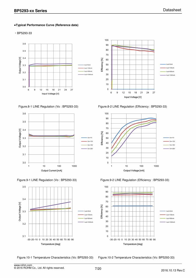
Typical Performance Curve (Reference data)
・BP5293-33
Figure.8-1 LINE Regulation (Vo : BP5293-33) Figure.8-2 LINE Regulation (Efficiency : BP5293-33)
Figure.9-1 LINE Regulation (Vo : BP5293-33) Figure.9-2 LINE Regulation (Efficiency : BP5293-33)
Figure.10-1 Temperature Characteristics (Vo: BP5293-33) Figure.10-2 Temperature Characteristics (Vo: BP5293-33)
3.0
3.1
3.2
3.3
3.4
3.5
3.6
6 9 12 15 18 21 24 27
Outp
ut V
oltag
e [V]
Input Voltage [V]
Iout=0mA
Iout=100mA
Iout=500mA
Iout=1000mA
0
10
20
30
40
50
60
70
80
90
100
6 9 12 15 18 21 24 27
Effic
ienc
y [%
]
Input Voltage [V]
Iout=0mA
Iout=100mA
Iout=500mA
Iout=1000mA
3.0
3.1
3.2
3.3
3.4
3.5
3.6
1 10 100 1000
Out
put V
olta
ge [V
]
Output Current [mA]
Vin=7V
Vin=12V
Vin=18V
Vin=26V
0
10
20
30
40
50
60
70
80
90
100
1 10 100 1000
Effic
ienc
y [%
]
Output Voltage [mA]
Vin=7V
Vin=12V
Vin=18V
Vin=26V
3.1
3.2
3.3
3.4
3.5
-30 -20-10 0 10 20 30 40 50 60 70 80 90
Out
put V
olta
ge [V
]
Temparature [deg]
Iout=2mA
Iout=100mA
Iout=500mA
Iout=1000mA
0
10
20
30
40
50
60
70
80
90
100
-30-20-10 0 10 20 30 40 50 60 70 80 90
Effic
ienc
y [%
]
Temparature [deg]
Iout=2mA
Iout=100mA
Iout=500mA
Iout=1000mA
8/20
DatasheetBP5293-xx Series
© 2016 ROHM Co., Ltd. All rights reserved. 2016.10.13 Rev.C
www.rohm.com
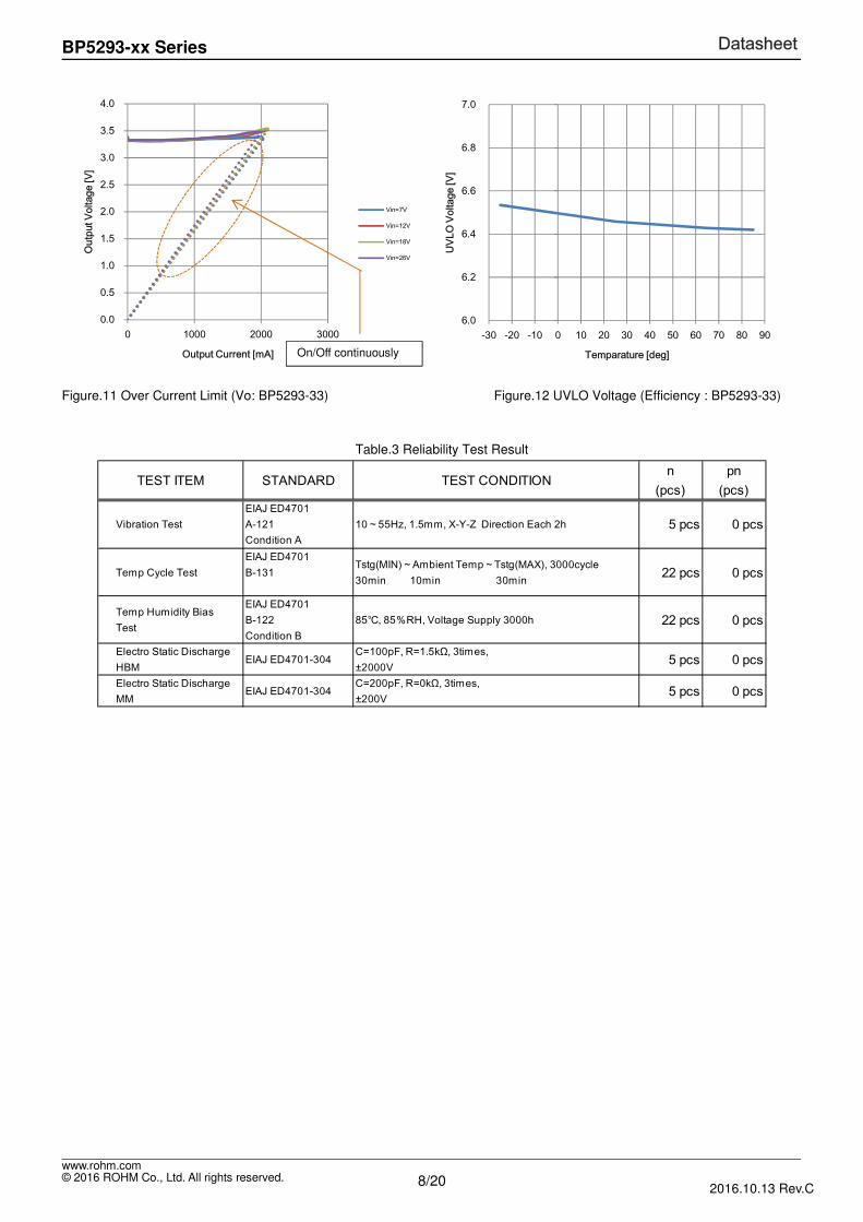
Figure.11 Over Current Limit (Vo: BP5293-33) Figure.12 UVLO Voltage (Efficiency : BP5293-33)
Table.3 Reliability Test Result
0.0
0.5
1.0
1.5
2.0
2.5
3.0
3.5
4.0
0 1000 2000 3000
Out
put V
olta
ge [V
]
Output Current [mA]
Vin=7V
Vin=12V
Vin=18V
Vin=26V
6.0
6.2
6.4
6.6
6.8
7.0
-30 -20 -10 0 10 20 30 40 50 60 70 80 90
UVL
O V
olta
ge [V
]
Temparature [deg]
TEST ITEM STANDARD TEST CONDITIONn
(pcs)pn
(pcs)
Vibration TestEIAJ ED4701A-121Condition A
10~55Hz, 1.5mm, X-Y-Z Direction Each 2h 5 pcs 0 pcs
Temp Cycle TestEIAJ ED4701B-131
Tstg(MIN)~Ambient Temp~Tstg(MAX), 3000cycle30min 10min 30min 22 pcs 0 pcs
Temp Humidity BiasTest
EIAJ ED4701B-122Condition B
85, 85%RH, Voltage Supply 3000h 22 pcs 0 pcs
Electro Static DischargeHBM
EIAJ ED4701-304C=100pF, R=1.5kΩ, 3times,±2000V 5 pcs 0 pcs
Electro Static DischargeMM
EIAJ ED4701-304C=200pF, R=0kΩ, 3times,±200V 5 pcs 0 pcs
On/Off continuously
9/20
DatasheetBP5293-xx Series
© 2016 ROHM Co., Ltd. All rights reserved. 2016.10.13 Rev.C
www.rohm.com
・BP5293-50
Figure.13-1 LINE Regulation (Vo: BP5293-50) Figure.13-2 LINE Regulation (Efficiency: BP5293-50)
Figure.14-1 LINE Regulation (Vo: BP5293-50) Figure.14-2 LINE Regulation (Efficiency: BP5293-50)
Figure.15-1 Temperature Characteristics (Vo: BP5293-50) Figure.15-2 Temperature Characteristics (Vo: BP5293-50)
4.8
4.9
5.0
5.1
5.2
6 9 12 15 18 21 24 27 30
Out
put V
olta
ge [V
]
Input Voltage [V]
Iout=0mA
Iout=100mA
Iout=500mA
Iout=1000mA
0
10
20
30
40
50
60
70
80
90
100
6 9 12 15 18 21 24 27
Effic
ienc
y [%
]
Input Voltage [V]
Iout=0mA
Iout=100mA
Iout=500mA
Iout=1000mA
4.8
4.9
5.0
5.1
5.2
1 10 100 1000
Out
put V
olta
ge [V
]
Output Current [mA]
Vin=7V
Vin=12V
Vin=18V
Vin=26V
0
10
20
30
40
50
60
70
80
90
100
1 10 100 1000
Effic
ienc
y [%
]
Output Voltage [mA]
Vin=7V
Vin=12V
Vin=18V
Vin=26V
4.8
4.9
5.0
5.1
5.2
-30-20-10 0 10 20 30 40 50 60 70 80 90
Out
put V
olta
ge [V
]
Temparature [deg]
Iout=2mA
Iout=100mA
Iout=500mA
Iout=1000mA
0
10
20
30
40
50
60
70
80
90
100
-30-20-10 0 10 20 30 40 50 60 70 80 90
Effic
ienc
y [%
]
Temparature [deg]
Iout=2mA
Iout=100mA
Iout=500mA
Iout=1000mA
10/20
DatasheetBP5293-xx Series
© 2016 ROHM Co., Ltd. All rights reserved. 2016.10.13 Rev.C
www.rohm.com
Figure.16 Over Current Limit (Vo: BP5293-50) Figure.17 UVLO Voltage (Efficiency: BP5293-50)
Table.4 Reliability Test Result
0.0
1.0
2.0
3.0
4.0
5.0
6.0
0 500 1000 1500 2000
Out
put V
olta
ge [V
]
Output Current [mA]
Vin=7V
Vin=12V
Vin=18V
Vin=26V
6.0
6.2
6.4
6.6
6.8
7.0
-30 -20 -10 0 10 20 30 40 50 60 70 80 90
UVL
O V
olta
ge [V
]
Temparature [deg]
TEST ITEM STANDARD TEST CONDITIONn
(pcs)pn
(pcs)
Vibration TestEIAJ ED4701A-121Condition A
10~55Hz, 1.5mm, X-Y-Z Direction Each 2h 5 pcs 0 pcs
Temp Cycle TestEIAJ ED4701B-131
Tstg(MIN)~Ambient Temp~Tstg(MAX), 3000cycle30min 10min 30min 22 pcs 0 pcs
Temp Humidity BiasTest
EIAJ ED4701B-122Condition B
85, 85%RH, Voltage Supply 3000h 22 pcs 0 pcs
Electro Static DischargeHBM
EIAJ ED4701-304C=100pF, R=1.5kΩ, 3times,±2000V 5 pcs 0 pcs
Electro Static DischargeMM
EIAJ ED4701-304C=200pF, R=0kΩ, 3times,±200V 5 pcs 0 pcs
On/Off continuously
11/20
DatasheetBP5293-xx Series
© 2016 ROHM Co., Ltd. All rights reserved. 2016.10.13 Rev.C
www.rohm.com
・BP5293-12
Figure.18-1 LINE Regulation (Vo : BP5293-12) Figure.18-2 LINE Regulation (Efficiency : BP5293-12)
Figure.19-1 LINE Regulation (Vo: BP5293-12) Figure.19-2 LINE Regulation (Efficiency: BP5293-12)
Figure.20-1 Temperature Characteristics (Vo: BP5293-12) Figure.20-2 Temperature Characteristics (Vo: BP5293-12)
11.0
11.2
11.4
11.6
11.8
12.0
12.2
12.4
12.6
12.8
13.0
15 18 21 24 27
Out
put V
olta
ge [V
]
Input Voltage [V]
Iout=0mA
Iout=100mA
Iout=500mA
Iout=1000mA
0
10
20
30
40
50
60
70
80
90
100
15 18 21 24 27
Effic
ienc
y [%
]
Input Voltage [V]
Iout=0mA
Iout=100mA
Iout=500mA
Iout=1000mA
11.0
11.2
11.4
11.6
11.8
12.0
12.2
12.4
12.6
12.8
13.0
1 10 100 1000
Out
put V
olta
ge [V
]
Output Current [mA]
Vin=17V
Vin=20V
Vin=24V
Vin=26V
0
10
20
30
40
50
60
70
80
90
100
1 10 100 1000
Effic
ienc
y [%
]
Output Voltage [mA]
Vin=17V
Vin=20V
Vin=24V
Vin=26V
11.0
11.2
11.4
11.6
11.8
12.0
12.2
12.4
12.6
12.8
13.0
-30-20-10 0 10 20 30 40 50 60 70 80 90
Out
put V
olta
ge [V
]
Temparature [deg]
Iout=2mA
Iout=100mA
Iout=500mA
Iout=1000mA
0
10
20
30
40
50
60
70
80
90
100
-30-20-10 0 10 20 30 40 50 60 70 80 90
Effic
ienc
y [%
]
Temparature [deg]
Iout=2mA
Iout=100mA
Iout=500mA
Iout=1000mA
12/20
DatasheetBP5293-xx Series
© 2016 ROHM Co., Ltd. All rights reserved. 2016.10.13 Rev.C
www.rohm.com
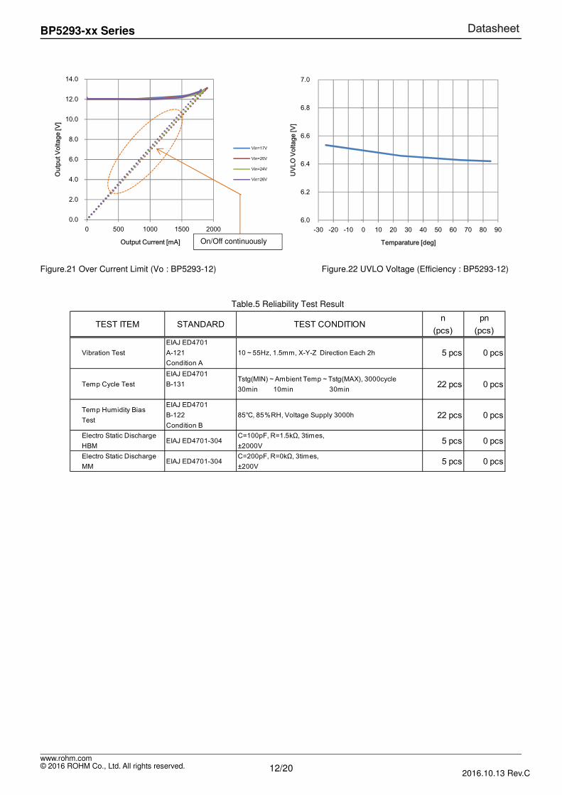
Figure.21 Over Current Limit (Vo : BP5293-12) Figure.22 UVLO Voltage (Efficiency : BP5293-12)
Table.5 Reliability Test Result
0.0
2.0
4.0
6.0
8.0
10.0
12.0
14.0
0 500 1000 1500 2000
Out
put V
olta
ge [V
]
Output Current [mA]
Vin=17V
Vin=20V
Vin=24V
Vin=26V
6.0
6.2
6.4
6.6
6.8
7.0
-30 -20 -10 0 10 20 30 40 50 60 70 80 90
UVL
O V
olta
ge [V
]
Temparature [deg]
TEST ITEM STANDARD TEST CONDITIONn
(pcs)pn
(pcs)
Vibration TestEIAJ ED4701A-121Condition A
10~55Hz, 1.5mm, X-Y-Z Direction Each 2h 5 pcs 0 pcs
Temp Cycle TestEIAJ ED4701B-131
Tstg(MIN)~Ambient Temp~Tstg(MAX), 3000cycle30min 10min 30min 22 pcs 0 pcs
Temp Humidity BiasTest
EIAJ ED4701B-122Condition B
85, 85%RH, Voltage Supply 3000h 22 pcs 0 pcs
Electro Static DischargeHBM
EIAJ ED4701-304C=100pF, R=1.5kΩ, 3times,±2000V 5 pcs 0 pcs
Electro Static DischargeMM
EIAJ ED4701-304C=200pF, R=0kΩ, 3times,±200V 5 pcs 0 pcs
On/Off continuously
13/20
DatasheetBP5293-xx Series
© 2016 ROHM Co., Ltd. All rights reserved. 2016.10.13 Rev.C
www.rohm.com
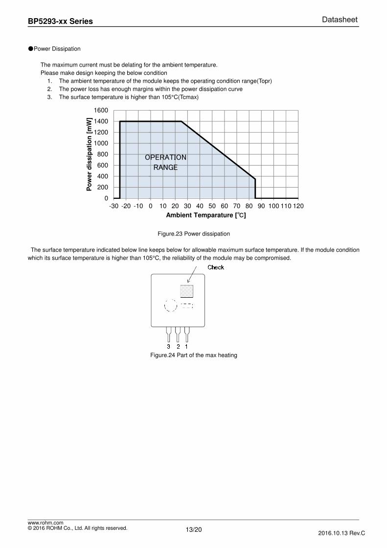
Power Dissipation
The maximum current must be delating for the ambient temperature.
Please make design keeping the below condition
1. The ambient temperature of the module keeps the operating condition range(Topr)
2. The power loss has enough margins within the power dissipation curve
3. The surface temperature is higher than 105°C(Tcmax)
Figure.23 Power dissipation
The surface temperature indicated below line keeps below for allowable maximum surface temperature. If the module condition
which its surface temperature is higher than 105°C, the reliability of the module may be compromised.
Figure.24 Part of the max heating
0
200
400
600
800
1000
1200
1400
1600
-30 -20 -10 0 10 20 30 40 50 60 70 80 90 100 110 120
Po
wer
dis
sip
ati
on
[m
W]
Ambient Temparature []
OPERATION
RANGE
14/20
DatasheetBP5293-xx Series
© 2016 ROHM Co., Ltd. All rights reserved. 2016.10.13 Rev.C
www.rohm.com
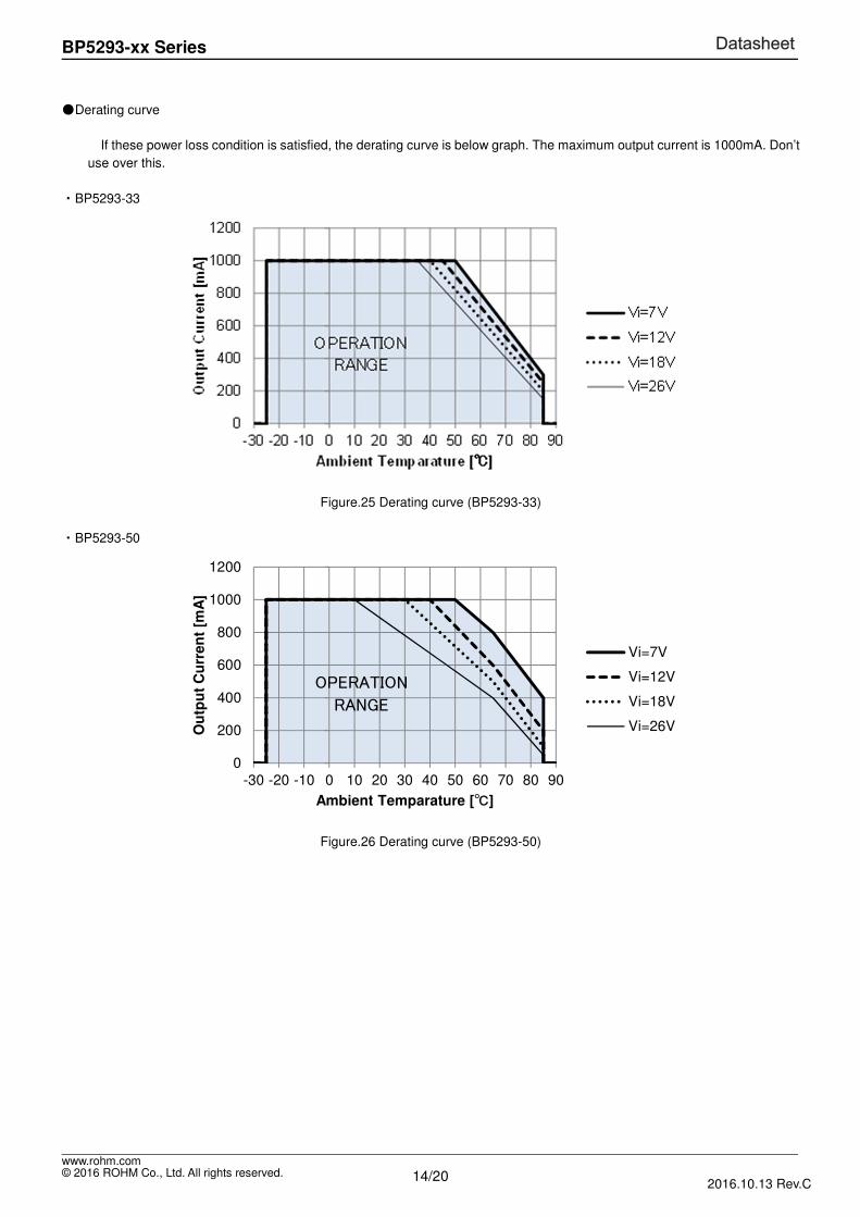
Derating curve
If these power loss condition is satisfied, the derating curve is below graph. The maximum output current is 1000mA. Don’t
use over this.
・BP5293-33
Figure.25 Derating curve (BP5293-33)
・BP5293-50
Figure.26 Derating curve (BP5293-50)
0
200
400
600
800
1000
1200
-30 -20 -10 0 10 20 30 40 50 60 70 80 90
Ou
tpu
t C
urr
en
t [m
A]
Ambient Temparature []
Vi=7V
Vi=12V
Vi=18V
Vi=26V
OPERATION
RANGE
15/20
DatasheetBP5293-xx Series
© 2016 ROHM Co., Ltd. All rights reserved. 2016.10.13 Rev.C
www.rohm.com
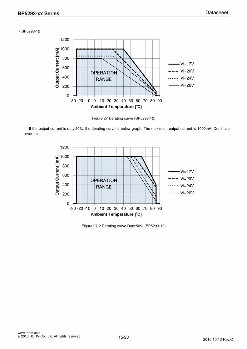
・BP5293-12
Figure.27 Derating curve (BP5293-12)
If the output current is duty;50%, the derating curve is below graph. The maximum output current is 1000mA. Don’t use
over this.
Figure.27-2 Derating curve Duty:50% (BP5293-12)
0
200
400
600
800
1000
1200
-30 -20 -10 0 10 20 30 40 50 60 70 80 90
Ou
tpu
t C
urr
en
t [m
A]
Ambient Temparature []
Vi=17V
Vi=20V
Vi=24V
Vi=26V
OPERATION
RANGE
0
200
400
600
800
1000
1200
-30 -20 -10 0 10 20 30 40 50 60 70 80 90
Ou
tpu
t C
urr
en
t [m
A]
Ambient Temparature []
Vi=17V
Vi=20V
Vi=24V
Vi=26V
OPERATION
RANGE
16/20
DatasheetBP5293-xx Series
© 2016 ROHM Co., Ltd. All rights reserved. 2016.10.13 Rev.C
www.rohm.com
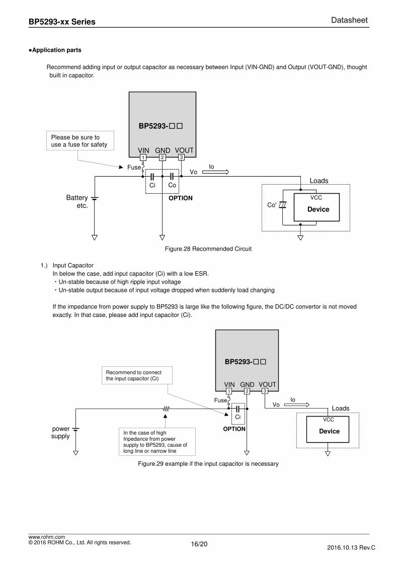
Application parts
Recommend adding input or output capacitor as necessary between Input (VIN-GND) and Output (VOUT-GND), thought
built in capacitor.
Figure.28 Recommended Circuit
1.) Input Capacitor
In below the case, add input capacitor (Ci) with a low ESR.
・Un-stable because of high ripple input voltage
・Un-stable output because of input voltage dropped when suddenly load changing
If the impedance from power supply to BP5293 is large like the following figure, the DC/DC convertor is not moved
exactly. In that case, please add input capacitor (Ci).
Figure.29 example if the input capacitor is necessary
BP5293-
GND
Fuse
Batteryetc.
VOUT1
VIN
Device
VCC
VoIo
Ci Co
OPTION
Please be sure to use a fuse for safety
2 3
Co'
Loads
BP5293-
GND
Fuse
powersupply
VOUT1
VIN
Device
VCC
VoIo
Ci
OPTION
Recommend to connect the input capacitor (Ci)
2 3
In the case of high Inpedance from power supply to BP5293, cause of long line or narrow line
Loads
17/20
DatasheetBP5293-xx Series
© 2016 ROHM Co., Ltd. All rights reserved. 2016.10.13 Rev.C
www.rohm.com
2.) Output Capacitor
In below the case, add output capacitor (Co) with a low ESR.
・High ripple voltage
・large changing output voltage, when suddenly load changing
・Un-stable output voltage unusually
If output capacitor Co' of the big capacity is connected and the VOUT voltage rise up (the time of soft-start mode), it's a load electric current in, rising of a VOUT voltage become late. Because of an over-current limiter functions by the electric current and the load electric current charged to an output capacitor. When rising of a VOUT voltage become late, the short-circuit protection sometimes moves. In that case, it isn’t
normally output any more. Please confirm that input current is less than 1.9A so that an over-current limiter doesn’t function.
Figure.30-1 normally start waveform if Co’ is small Figure.30-2 abnormal start waveform if Co’ is large
If a large Co’ is used, while charging to output capacitor, need to reduce load current. And after decrease charge current to
output capacitor, following load current. It is prevent current limiter, and it’s ordinarily possible to move.
Figure.30-3 Recommended waveform if Co’is big value
3.) Fuse
Please design safely with fail-safe design not to occur danger or damage, if module is broken by any chance. Connect
the “Fuse” adapted specification of input current for protecting continuous over current.
If VIN-GND is shorted accidentally, VOUT terminal may be supplied over voltage. If it’s supplied over voltage over 26V,
VOUT terminal is broken, and if 3A over current continuously, the module is heat, then smoke or ignition. Please connect
the “Fuse” 3A below.
Soft Start Time2.5msec(typ.)
Vo
IntputVoltage
Iomax : 1A
IntputCurrent
OutputVoltage (Vo)
OutputCurrent (Io)
6.6V typ.
1.9A
Soft Start Time2.5msec(typ.)
IntputVoltage
Iomax : 1A
IntputCurrent
OutputVoltage (Vo)
OutputCurrent (Io)
6.6V typ.
1.9A
Load Current : 1A
Charge Current foroutput capacitor(Co')
Vscp
OCP detected
SCP Detection Time0.9msec(typ.)
SCP detected
Soft Start Time2.5msec(typ.)
IntputVoltage
Iomax : 1A
IntputCurrent
OutputVoltage (Vo)
OutputCurrent (Io)
6.6V typ.
1.9A
Load Current : 0ACharge Current foroutput capacitor(Co')
Vscp
OCP Un-detected
SCP Un-detected
Load Current : 1A
Vo
18/20
DatasheetBP5293-xx Series
© 2016 ROHM Co., Ltd. All rights reserved. 2016.10.13 Rev.C
www.rohm.com
Dimensions
Fig.31 Dimensions
・The externals inspection standard is assumed to be a ROHM standard.
・Burr is not covered in above dimension value or tolerance.
・The dimension value without tolerance is a design value. (A=1.2mmMAX)
Marking
Pin No.1 Mark
ROHM Trade Mark
BP5293- Type name
1604* Production Lot Number 04th week of 2016
S:ROHM DALIAN
Structure
Fig.32 Structure
・ Soldering condition
Flow soldering 260°C within 10sec
Manual soldering 380°C within 3sec
・ Recommended land dimensions
Hole diameter 1.2mm
Land diameter 2.2mm (Please do cutting land when the interval of the pin is necessary)
Coil
Glass epoxy PC board
UL94V-0
Metal Lead Pin
Semiconductor
Ceramic capacitor
Chip resistor
Epoxy resin
19/20
DatasheetBP5293-xx Series
© 2016 ROHM Co., Ltd. All rights reserved. 2016.10.13 Rev.C
www.rohm.com
Packing Specification
48 pieces of modules might be packaged in the packaging tray, and it might be piled up 5steps, and with an empty pack on the top, in principle. The number of piling might change according to the quantity of delivery without previous notice. It is necessary to mount by hand.
Fig.33 Method of Packing
Manufacturing Factory
ROHM ELECTRONICS DALIAN CO.,LTD. (CHINA)
Tray
4pcs tape stop end
Tray in the case, and 1 tape end
5step +1 empty tray
20/20
DatasheetBP5293-xx Series
© 2016 ROHM Co., Ltd. All rights reserved. 2016.10.13 Rev.C
www.rohm.com
Caution on use
1. Although the power supply is paid much attention for quality control, it might be deteriorated or destructed in case it is
used beyond the absolute maximum rated value of applied voltage and the operating temperature range. When designing,
it should be used in a guarantee range in any case. It might get damaged if used beyond the absolute maximum value of
applied voltage and the operating temperature range. In case of damage, the applied mode such as short mode and open
mode cannot be specified, therefore please take physical safety measures including the fuse when the special mode
which exceeds the absolute maximum rated value is assumed.
2. The GND terminal should be set at the minimum electric potential in any operating conditions.
3. Please design the heat with enough allowance considering derating in the actual use state.
4. The power supply may be damaged because of the excessive stress on the substrate When the lead pin is bent.Please
use the lead pin without bending it.
5. At the time of starting the power supply, please set the output light loaded. The power supply line noise and the
voltage drop occured by the motion electric current should be within the hysteresis width of UVLO. When noises more than
hysteresis width are input, I may cause malfunction.
6. The power supply is not designed for vehicle installation,military use and equipment affect human life, please do not use it
for these purposes. In case used for the said purposes, we do not take any responsibility for the matters not meeting the
requirements.
7. The operating temperature range guarantees the function of the power supply, and is not to guarantee the life of it in the
range. Since the life of the power supply is subject to derating in accordance with the usage environment such as applied
voltage, ambient temperature, and the humidity, please perform the equipment design considering derating.
Notice
This document may not be reprinted or reproduced, in whole or in part, without prior written consent of ROHM.
This document is reference document. Please check the fomal specification by requesting other document.