Embed Size (px)
Citation preview
DatasheetSiC Power Module
BSM120C12P2C201
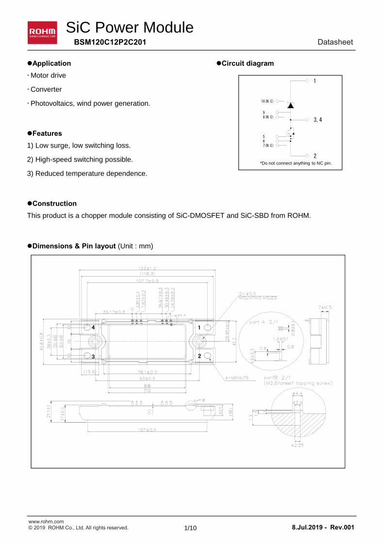
Application Circuit diagramMotor drive
Converter
Photovoltaics, wind power generation.
Features1) Low surge, low switching loss.
2) High-speed switching possible.
3) Reduced temperature dependence.
ConstructionThis product is a chopper module consisting of SiC-DMOSFET and SiC-SBD from ROHM.
Dimensions & Pin layout (Unit : mm)
1
3,4
2
7(N.C)65
8(N.C)9
10(N.C)
*Do not connect anything to NC pin.
5 6 7 8 9 10
1
2
4
3
1/10 8.Jul.2019 - Rev.001www.rohm.com© 2019 ROHM Co., Ltd. All rights reserved.
DatasheetBSM120C12P2C201
Absolute maximum ratings (Tj = 25°C)
Symbol Unit
VDSS G-S short
Repetitive reverse voltage VDSS Clamp diode
G - S Voltage (tsurge<300ns) VGSS_surge D-S short
ID DC (Tc=60°C)
IDRM Pulse (Tc=60°C) 1ms *2
IDRM Pulse (Tc=60°C) 10us *2
IS DC (Tc=60°C ) VGS=18V
ISRM
ISRM
IF DC (Tc=60°C ) VGS=18V
IFRM
IFRM
Total power disspation *4 Ptot Tc=25°C W
Max Junction Temperature Tjmax
Tjop
Tstg
Main Terminals : M6 screw
(*1) Case temperature (Tc) is defined on the surface of base plate just under the chips.
(*2) Repetition rate should be kept within the range where temperature rise if die should not exceed Tj max.
(*3) Tj is less than 175°C
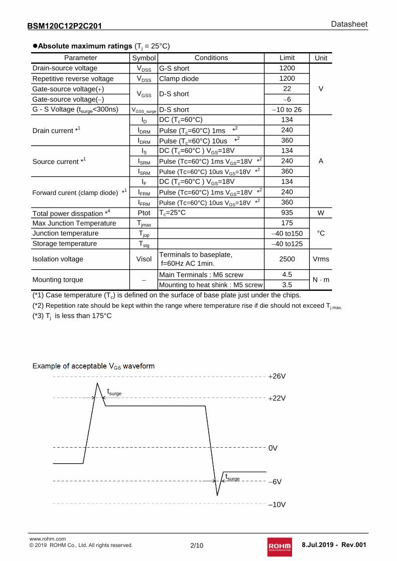
Example of acceptable VGS waveform
Conditions
240
1200
Forward curent (clamp diode) *1
134
Pulse (Tc=60°C) 1ms VGS=18V *2 240
Pulse (Tc=60°C) 10us VGS=18V *2 360
Limit
1200
22
6
134
10 to 26
Parameter
Drain-source voltage
Gate-source voltage()
Gate-source voltage()
Junction temperature
Drain current *1
Pulse (Tc=60°C) 10us VGS=18V *2
Source current *1
VGSS D-S short
Mounting torque
Isolation voltage
Mounting to heat shink : M5 screw
Storage temperature
Pulse (Tc=60°C) 1ms VGS=18V *2
VisolTerminals to baseplate, f=60Hz AC 1min.
V
175
°C
N · m
Vrms
4.5
3.5
935
40 to150
40 to125
2500
240
360
134
360
A
26V
0V
6V
10V
22Vtsurge
tsurge
2/10 8.Jul.2019 - Rev.001
www.rohm.com© 2019 ROHM Co., Ltd. All rights reserved.
DatasheetBSM120C12P2C201
Electrical characteristics (Tj=25°C)
Symbol Min. Typ. Max. Unit
Tj=25°C - 2.1 3.2
Tj=125°C - 3.1 -Tj=150°C - 3.4 5.2
IDSS - - 10 ATj=25°C - 1.7 2.1
Tj=125°C 2.2 -
Tj=150°C - 2.4 3.2
IRRM - - 2 mA
VGS(th) 1.6 - 4 V
- - 0.5
0.5 - -td(on) - 30 -
tr - 40 -trr - 20 -
td(off) - 165 -tf - 45 -
Ciss VDS=10V, VGS=0V, 1MHz - 14 - nF
Gate Registance RGint Tj=25°C - 1.8 - Stray Inductance Ls 25 - nH
Terminal to heat sink 12.5 - mm
Terminal to terminal 20 - mm
Terminal to heat sink 10.5 - mm
Terminal to terminal 14 - mm
DMOS (1/2 module) *4 - - 0.16
SBD (1/2 module) *4 - - 0.21
(*4) Measurement of Tc is to be done at the point just under the chip.(*5) Typical value is measured by using thermally conductive grease of λ=0.9W/(m・K).(*6) SiC devices have lower short cuicuit withstand capability due to high current density. Please be advised to pay careful attention to short cuicuit accident and try to adjust protection time to shutdown them as short as possible.(*7) If the Product is used beyond absolute maximum ratings defined in the Specifications, as its internal structure may be dameged, please replace such Product with a new one.
°C/W
Drain cutoff current VDS=1200V, VGS=0V
Forwad Voltage VF IF=120A V
-
-
Gate-source leakage current IGSSVGS=22V, VDS=0V
VGS= 6V, VDS=0V
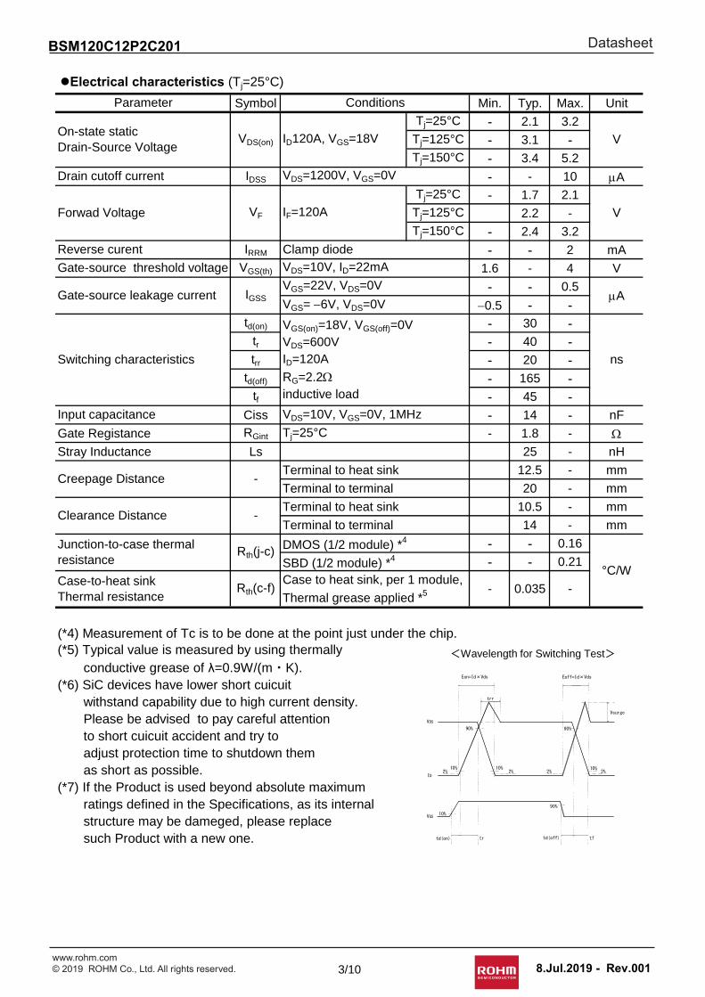
Switching characteristics
VGS(on)=18V, VGS(off)=0VVDS=600VID=120A
RG=2.2inductive load
Gate-source threshold voltage
Parameter Conditions
On-state staticDrain-Source Voltage
VDS(on) ID120A, VGS=18V
VDS=10V, ID=22mA
V
A
ns
Reverse curent Clamp diode
-
Input capacitance
Junction-to-case thermalresistance
Rth(j-c)
Creepage Distance
Clearance Distance
Case-to-heat sinkThermal resistance
Rth(c-f)Case to heat sink, per 1 module,
Thermal grease applied *5 - 0.035
ID
VDS
10%
VGS10%
90%
10% 10%
90%
Eon=Id×Vds
2%
td(on) tr
2%
trr
90%
2%2%
Eoff=Id×Vds
td(off) tf
Vsurge
<Wavelength for Switching Test>
3/10 8.Jul.2019 - Rev.001
www.rohm.com© 2019 ROHM Co., Ltd. All rights reserved.
DatasheetBSM120C12P2C201
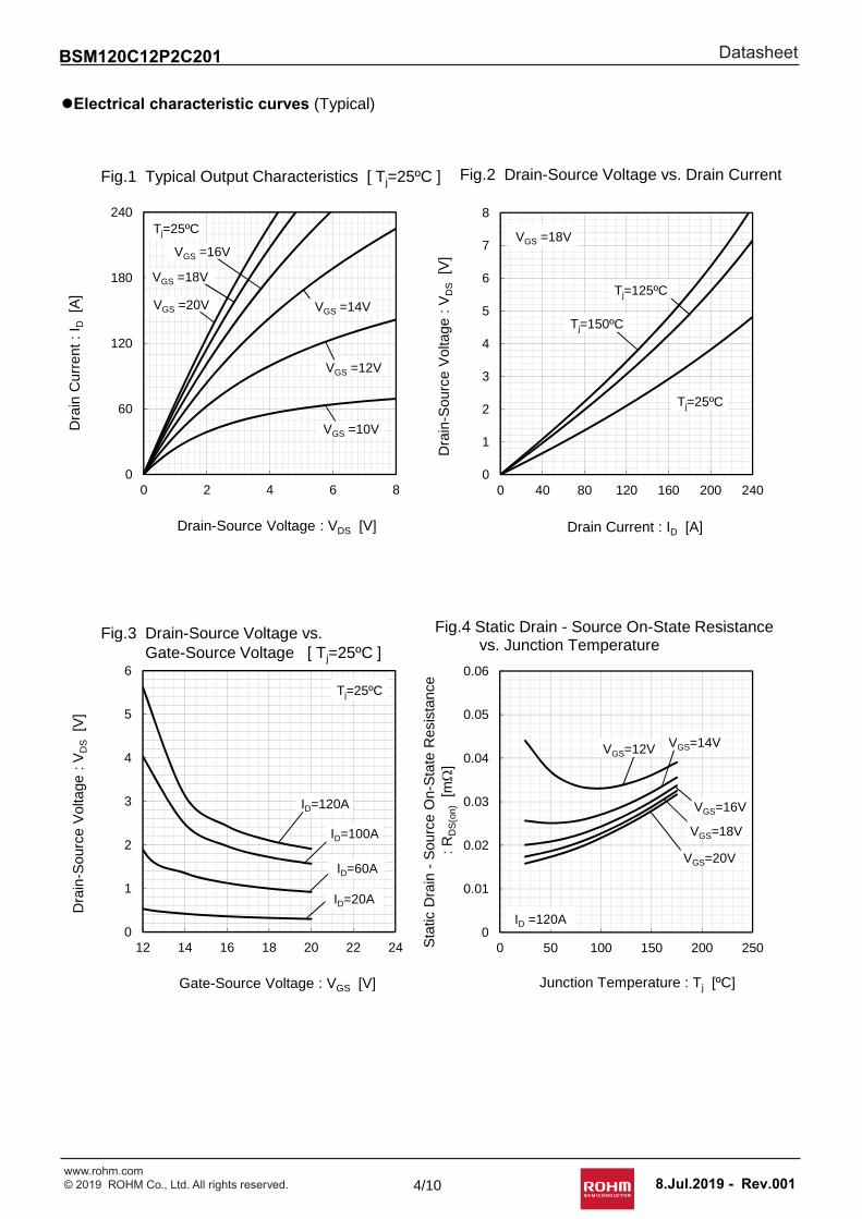
Electrical characteristic curves (Typical)
Fig.1 Typical Output Characteristics [ Tj=25ºC ]
Dra
in C
urre
nt :
ID
[A]
Drain-Source Voltage : VDS [V]
Fig.2 Drain-Source Voltage vs. Drain Current
Dra
in-S
ourc
e V
olta
ge :
VD
S[V
]
Drain Current : ID [A]
Fig.3 Drain-Source Voltage vs. Gate-Source Voltage [ Tj=25ºC ]
Dra
in-S
ourc
e V
olta
ge :
VD
S[V
]
Gate-Source Voltage : VGS [V] Junction Temperature : Tj [ºC]
Sta
tic D
rain
-S
ourc
e O
n-S
tate
Res
ista
nce
: RD
S(o
n)[m
]
Fig.4 Static Drain - Source On-State Resistance vs. Junction Temperature
0
60
120
180
240
0 2 4 6 8
Tj=25ºC
VGS =16V
VGS =18V
VGS =20V VGS =14V
VGS =12V
VGS =10V
0
1
2
3
4
5
6
7
8
0 40 80 120 160 200 240
VGS =18V
Tj=25ºC
Tj=125ºC
Tj=150ºC
0
1
2
3
4
5
6
12 14 16 18 20 22 24
ID=120A
Tj=25ºC
ID=100A
ID=60A
ID=20A
0
0.01
0.02
0.03
0.04
0.05
0.06
0 50 100 150 200 250
ID =120A
VGS=12V VGS=14V
VGS=16V
VGS=18V
VGS=20V
4/10 8.Jul.2019 - Rev.001
www.rohm.com© 2019 ROHM Co., Ltd. All rights reserved.
DatasheetBSM120C12P2C201
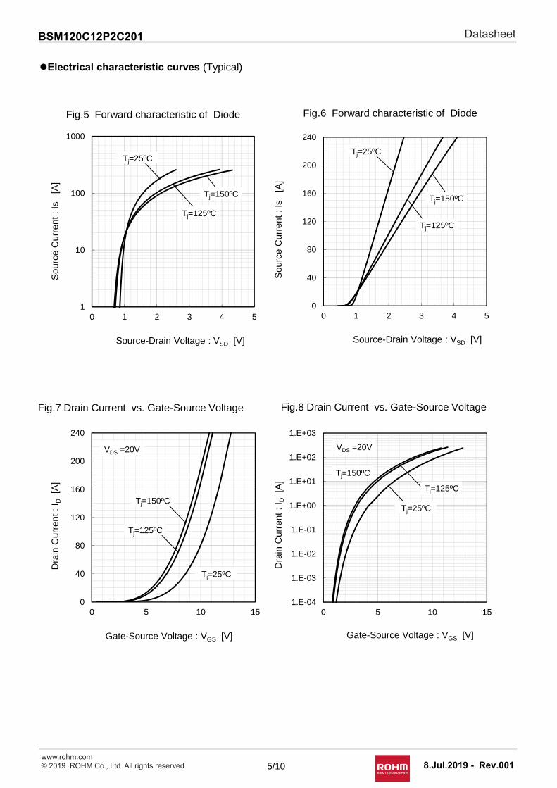
Electrical characteristic curves (Typical)
Fig.6 Forward characteristic of Diode
Sou
rce
Cur
rent
: Is
[A
]
Source-Drain Voltage : VSD [V]
Gate-Source Voltage : VGS [V]
Fig.7 Drain Current vs. Gate-Source Voltage
Dra
in C
urre
nt :
ID
[A]
Fig.8 Drain Current vs. Gate-Source Voltage
Dra
in C
urre
nt :
ID
[A]
Gate-Source Voltage : VGS [V]
Fig.5 Forward characteristic of Diode
Sou
rce
Cur
rent
: Is
[A
]
Source-Drain Voltage : VSD [V]
1
10
100
1000
0 1 2 3 4 5
Tj=125ºC
Tj=25ºC
Tj=150ºC
0
40
80
120
160
200
240
0 1 2 3 4 5
Tj=125ºC
Tj=150ºC
Tj=25ºC
0
40
80
120
160
200
240
0 5 10 15
VDS =20V
Tj=25ºC
Tj=125ºC
Tj=150ºC
1.E-04
1.E-03
1.E-02
1.E-01
1.E+00
1.E+01
1.E+02
1.E+03
0 5 10 15
Tj=25ºC
Tj=125ºC
VDS =20V
Tj=150ºC
5/10 8.Jul.2019 - Rev.001
www.rohm.com© 2019 ROHM Co., Ltd. All rights reserved.
DatasheetBSM120C12P2C201
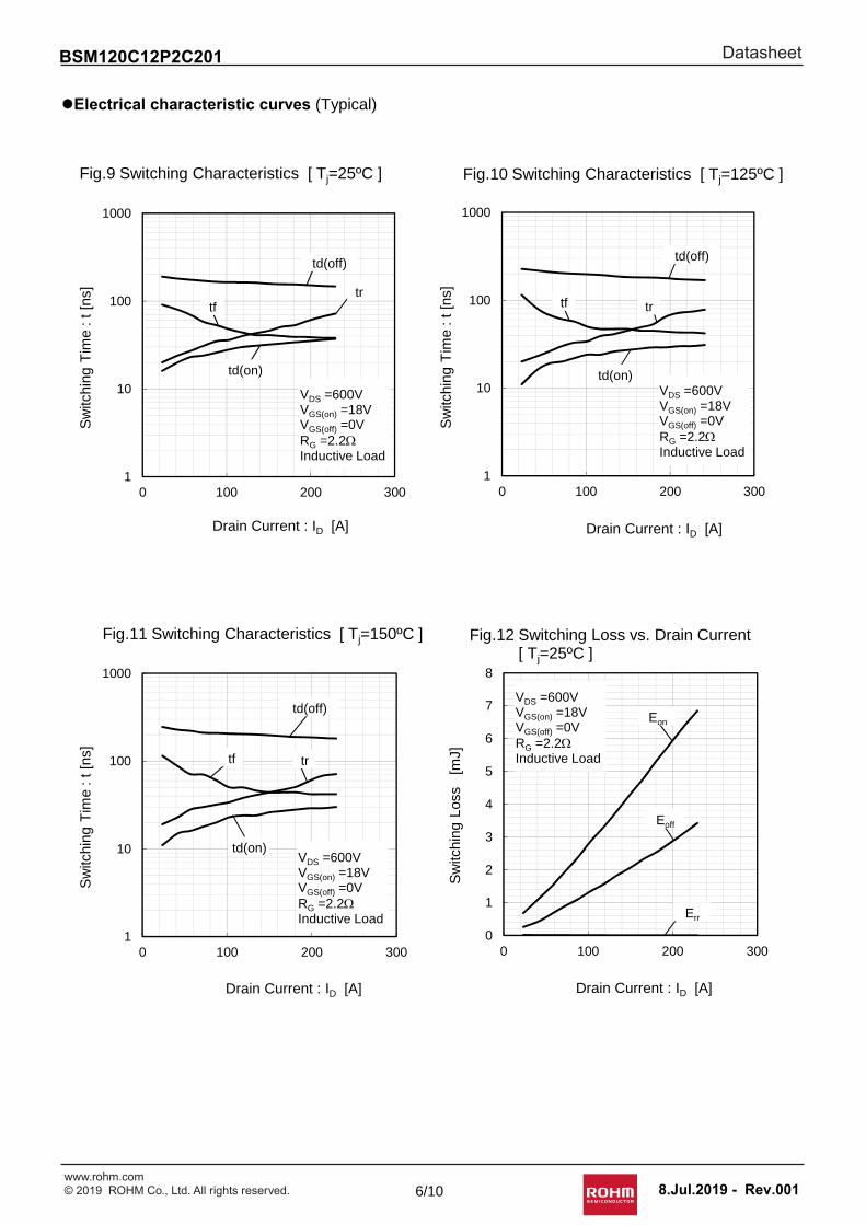
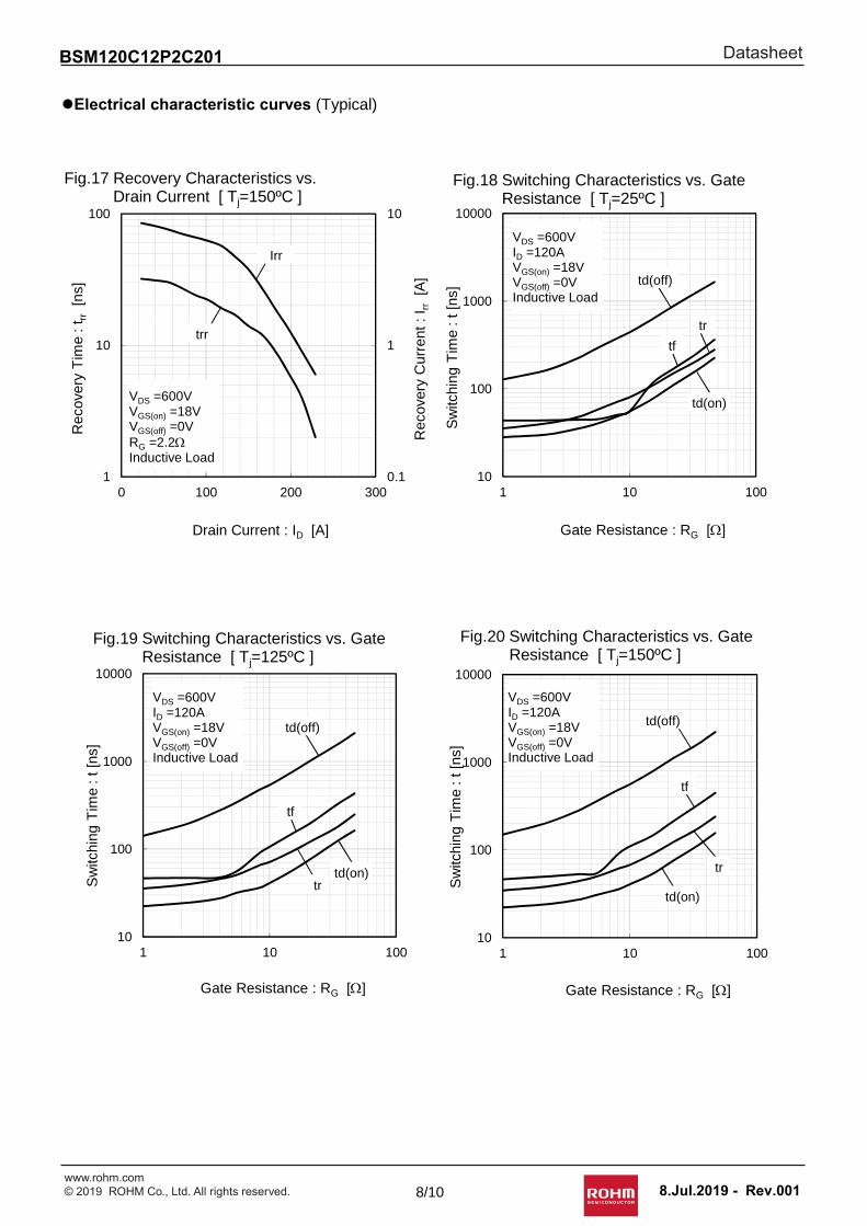
Electrical characteristic curves (Typical)
Fig.12 Switching Loss vs. Drain Current [ Tj=25ºC ]
Drain Current : ID [A]
Fig.10 Switching Characteristics [ Tj=125ºC ]
Sw
itchi
ng T
ime
: t [
ns]
Drain Current : ID [A]
Sw
itchi
ng L
oss
[m
J]
Drain Current : ID [A]
Fig.9 Switching Characteristics [ Tj=25ºC ]
Sw
itchi
ng T
ime
: t [
ns]
Fig.11 Switching Characteristics [ Tj=150ºC ]
Sw
itchi
ng T
ime
: t [
ns]
Drain Current : ID [A]
1
10
100
1000
0 100 200 300
tf
td(off)
tr
td(on)VDS =600VVGS(on) =18VVGS(off) =0VRG =2.2Inductive Load
1
10
100
1000
0 100 200 300
tf
td(off)
tr
td(on)
VDS =600VVGS(on) =18VVGS(off) =0VRG =2.2Inductive Load
0
1
2
3
4
5
6
7
8
0 100 200 300
Eon
Eoff
Err
VDS =600VVGS(on) =18VVGS(off) =0VRG =2.2Inductive Load
1
10
100
1000
0 100 200 300
td(off)
tr
td(on)
tf
VDS =600VVGS(on) =18VVGS(off) =0VRG =2.2Inductive Load
6/10 8.Jul.2019 - Rev.001
www.rohm.com© 2019 ROHM Co., Ltd. All rights reserved.
DatasheetBSM120C12P2C201
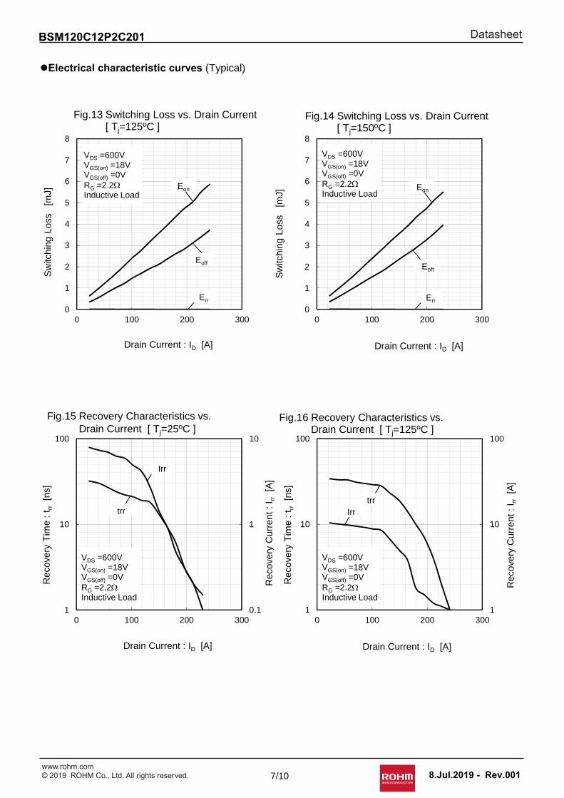
Electrical characteristic curves (Typical)
Drain Current : ID [A]
Fig.16 Recovery Characteristics vs.Drain Current [ Tj=125ºC ]
Rec
over
y T
ime
: t rr
[ns]
Rec
over
y C
urre
nt :
I rr
[A]
Rec
over
y C
urre
nt :
I rr
[A]
Rec
over
y T
ime
: t rr
[ns]
Fig.15 Recovery Characteristics vs.Drain Current [ Tj=25ºC ]
Drain Current : ID [A]
Fig.14 Switching Loss vs. Drain Current [ Tj=150ºC ]
Sw
itchi
ng L
oss
[m
J]
Drain Current : ID [A]
Fig.13 Switching Loss vs. Drain Current [ Tj=125ºC ]
Sw
itchi
ng L
oss
[m
J]
Drain Current : ID [A]
0
1
2
3
4
5
6
7
8
0 100 200 300
Eon
Eoff
Err
VDS =600VVGS(on) =18VVGS(off) =0VRG =2.2Inductive Load
1
10
100
1
10
100
0 100 200 300
VDS =600VVGS(on) =18VVGS(off) =0VRG =2.2Inductive Load
Irrtrr
0.1
1
10
1
10
100
0 100 200 300
VDS =600VVGS(on) =18VVGS(off) =0VRG =2.2Inductive Load
Irr
trr
0
1
2
3
4
5
6
7
8
0 100 200 300
Eon
Eoff
Err
VDS =600VVGS(on) =18VVGS(off) =0VRG =2.2Inductive Load
7/10 8.Jul.2019 - Rev.001
www.rohm.com© 2019 ROHM Co., Ltd. All rights reserved.
DatasheetBSM120C12P2C201
Electrical characteristic curves (Typical)S
witc
hing
Tim
e : t
[ns
]
Gate Resistance : RG []
Fig.19 Switching Characteristics vs. Gate Resistance [ Tj=125ºC ]
Gate Resistance : RG []
Fig.20 Switching Characteristics vs. Gate Resistance [ Tj=150ºC ]
Sw
itchi
ng T
ime
: t [
ns]
Sw
itchi
ng T
ime
: t [
ns]
Gate Resistance : RG []
Fig.18 Switching Characteristics vs. Gate Resistance [ Tj=25ºC ]
Drain Current : ID [A]
Fig.17 Recovery Characteristics vs.Drain Current [ Tj=150ºC ]
Rec
over
y T
ime
: t rr
[ns]
Rec
over
y C
urre
nt :
I rr
[A]
10
100
1000
10000
1 10 100
td(off)
td(on)
VDS =600VID =120AVGS(on) =18VVGS(off) =0VInductive Load
tf
tr
10
100
1000
10000
1 10 100
td(off)
td(on)
VDS =600VID =120AVGS(on) =18VVGS(off) =0VInductive Load
tf
tr
0.1
1
10
1
10
100
0 100 200 300
VDS =600VVGS(on) =18VVGS(off) =0VRG =2.2Inductive Load
trr
Irr
10
100
1000
10000
1 10 100
VDS =600VID =120AVGS(on) =18VVGS(off) =0VInductive Load
td(off)
td(on)
tr
tf
8/10 8.Jul.2019 - Rev.001
www.rohm.com© 2019 ROHM Co., Ltd. All rights reserved.

DatasheetBSM120C12P2C201
Electrical characteristic curves (Typical)
Fig.24 Typical Capacitance vs. Drain-Source Voltage
Drain-Source Voltage : VDS [V]
Cap
asita
nce
: C
[F
]
Fig.22 Switching Loss vs. Gate Resistance [ Tj=125ºC ]
Sw
itchi
ng L
oss
[m
J]
Gate Resistance : RG []
Fig.23 Switching Loss vs. Gate Resistance [ Tj=150ºC ]
Sw
itchi
ng L
oss
[m
J]
Gate Resistance : RG []
Fig.21 Switching Loss vs. Gate Resistance [ Tj=25ºC ]
Sw
itchi
ng L
oss
[m
J]
Gate Resistance : RG []
0
10
20
30
1 10 100
VDS =600VID =120AVGS(on) =18VVGS(off) =0VInductive Load
Eon
Eoff
Err
0
10
20
30
1 10 100
VDS =600VID =120AVGS(on) =18VVGS(off) =0VInductive Load
Eon
Eoff
Err
0
10
20
30
1 10 100
VDS =600VID =120AVGS(on) =18VVGS(off) =0VInductive Load
Eon
Eoff
Err
1.E-11
1.E-10
1.E-09
1.E-08
1.E-07
0.01 0.1 1 10 100 1000
Tj=25ºCVGS =0V1MHz
Coss
Ciss
Crss
9/10 8.Jul.2019 - Rev.001
www.rohm.com© 2019 ROHM Co., Ltd. All rights reserved.
DatasheetBSM120C12P2C201
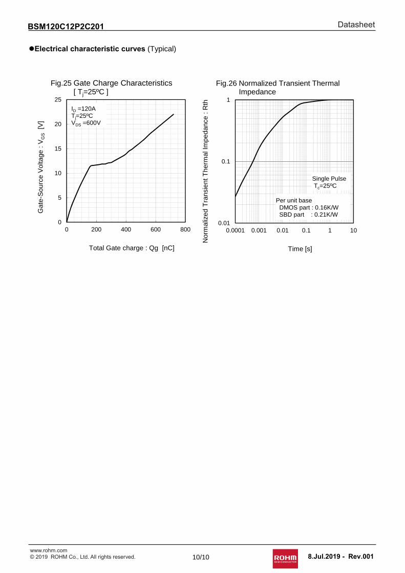
Electrical characteristic curves (Typical)
Time [s]
Fig.26 Normalized Transient Thermal Impedance
Nor
mal
ized
Tra
nsie
nt T
herm
al Im
peda
nce
: R
th
Fig.25 Gate Charge Characteristics [ Tj=25ºC ]
Gat
e-S
ourc
e V
olta
ge :
VG
S[V
]
Total Gate charge : Qg [nC]
0
5
10
15
20
25
0 200 400 600 800
ID =120ATj=25ºCVDS =600V
0.01
0.1
1
0.0001 0.001 0.01 0.1 1 10
Single PulseTc=25ºC
Per unit base DMOS part : 0.16K/WSBD part : 0.21K/W
10/10 8.Jul.2019 - Rev.001
www.rohm.com© 2019 ROHM Co., Ltd. All rights reserved.
R1107 Swww.rohm.com© 2012 ROHM Co., Ltd. All rights reserved.
Notice
ROHM Customer Support System http://www.rohm.com/contact/
Thank you for your accessing to ROHM product informations. More detail product informations and catalogs are available, please contact us.
N o t e s
The information contained herein is subject to change without notice.
Before you use our Products, please contact our sales representative and verify the latest specifica-tions.
Although ROHM is continuously working to improve product reliability and quality, semicon-ductors can break down and malfunction due to various factors.Therefore, in order to prevent personal injury or fire arising from failure, please take safety measures such as complying with the derating characteristics, implementing redundant and fire prevention designs, and utilizing backups and fail-safe procedures. ROHM shall have no responsibility for any damages arising out of the use of our Poducts beyond the rating specified by ROHM.
Examples of application circuits, circuit constants and any other information contained herein are provided only to illustrate the standard usage and operations of the Products. The peripheral conditions must be taken into account when designing circuits for mass production.
The technical information specified herein is intended only to show the typical functions of and examples of application circuits for the Products. ROHM does not grant you, explicitly or implicitly, any license to use or exercise intellectual property or other rights held by ROHM or any other parties. ROHM shall have no responsibility whatsoever for any dispute arising out of the use of such technical information.
The Products specified in this document are not designed to be radiation tolerant.
For use of our Products in applications requiring a high degree of reliability (as exemplified below), please contact and consult with a ROHM representative : transportation equipment (i.e. cars, ships, trains), primary communication equipment, traffic lights, fire/crime prevention, safety equipment, medical systems, and power transmission systems.
Do not use our Products in applications requiring extremely high reliability, such as aerospace equipment, nuclear power control systems, and submarine repeaters.
ROHM shall have no responsibility for any damages or injury arising from non-compliance with the recommended usage conditions and specifications contained herein.
ROHM has used reasonable care to ensure the accuracy of the information contained in this document. However, ROHM does not warrants that such information is error-free, and ROHM shall have no responsibility for any damages arising from any inaccuracy or misprint of such information.
Please use the Products in accordance with any applicable environmental laws and regulations, such as the RoHS Directive. For more details, including RoHS compatibility, please contact a ROHM sales office. ROHM shall have no responsibility for any damages or losses resulting non-compliance with any applicable laws or regulations.
When providing our Products and technologies contained in this document to other countries, you must abide by the procedures and provisions stipulated in all applicable export laws and regulations, including without limitation the US Export Administration Regulations and the Foreign Exchange and Foreign Trade Act.
This document, in part or in whole, may not be reprinted or reproduced without prior consent of ROHM.
1)
2)
3)
4)
5)
6)
7)
8)
9)
10)
11)
12)
13)

DatasheetDatasheet
Notice – WE Rev.001© 2015 ROHM Co., Ltd. All rights reserved.
General Precaution 1. Before you use our Pro ducts, you are requested to care fully read this document and fully understand its contents.
ROHM shall n ot be in an y way responsible or liabl e for fa ilure, malfunction or acci dent arising from the use of a ny ROHM’s Products against warning, caution or note contained in this document.
2. All information contained in this docume nt is current as of the issuing date and subj ect to change without any prior
notice. Before purchasing or using ROHM’s Products, please confirm the la test information with a ROHM sale s representative.
3. The information contained in this doc ument is provi ded on an “as is” basis and ROHM does not warrant that all
information contained in this document is accurate an d/or error-free. ROHM shall not be in an y way responsible or liable for any damages, expenses or losses incurred by you or third parties resulting from inaccuracy or errors of or concerning such information.


![Chapter 2 SiC Materials and Processing Technology€¦ · 34 2 SiC Materials and Processing Technology Table 2.1 Key electrical parameters of SiC [1] Property 4H-SiC 6H-SiC 3C-SiC](https://img.pdfslide.us/doc/110x75/5f4fd11797ddad63bf719816/chapter-2-sic-materials-and-processing-technology-34-2-sic-materials-and-processing.jpg)