Embed Size (px)
Citation preview

ExampleGuide7.0

FEKOExamples Guide
Suite 7.0
May 2014
Copyright 1998 – 2014: EM Software & Systems-S.A. (Pty) Ltd32 Techno Avenue, Technopark, Stellenbosch, 7600, South AfricaTel: +27-21-831-1500, Fax: +27-21-880-1936E-Mail: [email protected]: www.feko.info
CONTENTS i
Contents
Introduction . . . . . . . . . . . . . . . . . . . . . . . . . . . . . . . . . . . . . . . . . . . . 1
A Antenna synthesis + analysis
A-1 Dipole example . . . . . . . . . . . . . . . . . . . . . . . . . . . . . . . . . . . . . . . A-1-1
A-2 Dipole in front of a cube . . . . . . . . . . . . . . . . . . . . . . . . . . . . . . . . . A-2-1
A-3 Dipole in front of a plate . . . . . . . . . . . . . . . . . . . . . . . . . . . . . . . . . A-3-1
A-4 A monopole antenna on a finite ground plane . . . . . . . . . . . . . . . . . . . . A-4-1
A-5 Yagi-Uda antenna above a real ground . . . . . . . . . . . . . . . . . . . . . . . . . A-5-1
A-6 Pattern optimisation of a Yagi-Uda antenna . . . . . . . . . . . . . . . . . . . . . . A-6-1
A-7 Log periodic antenna . . . . . . . . . . . . . . . . . . . . . . . . . . . . . . . . . . . A-7-1
A-8 Microstrip patch antenna . . . . . . . . . . . . . . . . . . . . . . . . . . . . . . . . . A-8-1
A-9 Proximity coupled patch antenna with microstrip feed . . . . . . . . . . . . . . . A-9-1
A-10 Modelling an aperture coupled patch antenna . . . . . . . . . . . . . . . . . . . A-10-1
A-11 Different ways to feed a horn antenna . . . . . . . . . . . . . . . . . . . . . . . . A-11-1
A-12 Dielectric resonator antenna on finite ground . . . . . . . . . . . . . . . . . . . . A-12-1
A-13 A lens antenna with geometrical optics (GO) - ray launching . . . . . . . . . . A-13-1
A-14 Windscreen antenna on an automobile . . . . . . . . . . . . . . . . . . . . . . . . A-14-1
A-15 Design of a MIMO elliptical ring antenna (characteristic modes) . . . . . . . . A-15-1
A-16 Periodic boundary conditions for array analysis . . . . . . . . . . . . . . . . . . A-16-1
A-17 Finite array with non-linear element spacing . . . . . . . . . . . . . . . . . . . . A-17-1
B Antenna placement
B-1 Antenna coupling on an electrically large object . . . . . . . . . . . . . . . . . . . B-1-1
B-2 Antenna coupling using an ideal receiving antenna . . . . . . . . . . . . . . . . . B-2-1
B-3 Using a point source and ideal receiving antenna . . . . . . . . . . . . . . . . . . B-3-1
C Radar cross section (RCS)
C-1 RCS of a thin dielectric sheet . . . . . . . . . . . . . . . . . . . . . . . . . . . . . . . C-1-1
C-2 RCS and near field of a dielectric sphere . . . . . . . . . . . . . . . . . . . . . . . C-2-1
C-3 Scattering width of an infinite cylinder . . . . . . . . . . . . . . . . . . . . . . . . C-3-1
C-4 Periodic boundary conditions for FSS characterisation . . . . . . . . . . . . . . . C-4-1
D EMC analysis + cable coupling
D-1 Shielding factor of a sphere with finite conductivity . . . . . . . . . . . . . . . . D-1-1
May 2014 FEKO Examples Guide

CONTENTS ii
D-2 Calculating field coupling into a shielded cable . . . . . . . . . . . . . . . . . . . D-2-1
D-3 A magnetic-field probe . . . . . . . . . . . . . . . . . . . . . . . . . . . . . . . . . . D-3-1
D-4 Antenna radiation hazard (RADHAZ) safety zones . . . . . . . . . . . . . . . . . D-4-1
E Waveguide + microwave circuits
E-1 A Microstrip filter . . . . . . . . . . . . . . . . . . . . . . . . . . . . . . . . . . . . . . E-1-1
E-2 S-parameter coupling in a stepped waveguide section . . . . . . . . . . . . . . . E-2-1
E-3 Using a non-radiating network to match a dipole antenna . . . . . . . . . . . . . E-3-1
E-4 Subdividing a model using non-radiating networks . . . . . . . . . . . . . . . . . E-4-1
E-5 A Microstrip coupler . . . . . . . . . . . . . . . . . . . . . . . . . . . . . . . . . . . . E-5-1
F Bio electromagnetics
F-1 Exposure of muscle tissue using MoM/FEM hybrid . . . . . . . . . . . . . . . . . F-1-1
F-2 Magnetic Resonance Imaging (MRI) birdcage head coil example . . . . . . . . . F-2-1
G Time domain examples
G-1 Time analysis of the effect of an incident plane wave on an obstacle . . . . . . G-1-1
H Special solution methods
H-1 A Forked dipole antenna (continuous frequency range) . . . . . . . . . . . . . . H-1-1
H-2 Using the MLFMM for electrically large models . . . . . . . . . . . . . . . . . . . H-2-1
H-3 Horn feeding a large reflector . . . . . . . . . . . . . . . . . . . . . . . . . . . . . . H-3-1
H-4 Optimise waveguide pin feed location . . . . . . . . . . . . . . . . . . . . . . . . . H-4-1
I User interface tools
I-1 POSTFEKO Application automation . . . . . . . . . . . . . . . . . . . . . . . . . . . I-1-1
J Index
Index . . . . . . . . . . . . . . . . . . . . . . . . . . . . . . . . . . . . . . . . . . . . . . . . . I-1
May 2014 FEKO Examples Guide

INTRODUCTION 1
Introduction
This Examples guide presents a set of simple examples which demonstrate a selection of thefeatures of the FEKO Suite. The examples have been selected to illustrate the features withoutbeing unnecessarily complex or requiring excessive run times. The input files for the examplescan be found in the examples/ExampleGuide_models directory under the FEKO installation.No results are provided for these examples and in most cases, the *.pre, *.cfm and/or *.optfiles have to be generated by opening and re-saving the provided project files (*.cfx) before thecomputation of the results can be initiated by running the FEKO preprocessor, solver or optimiser.
FEKO can be used in one of three ways. The first and recommended way is to construct the entiremodel in the CADFEKO user interface. The second way is to use CADFEKO for the model geome-try creation and the solution set up and to use scripting for advanced options and adjustment ofthe model (for example the selection of advanced preconditioner options). The last way is to usethe scripting for the entire model geometry and solution set up.
In this document the focus is on the recommended approaches (primarily using the CADFEKOuser interface with no scripting).
Examples that employ only scripting are discussed in the Script Examples guide. These exam-ples illustrate similar applications and methods to the examples in the Examples guide and it ishighly recommended that you only consider the Script Examples if scripting-only examples arespecifically required. It is advisable to work through the Getting started guide and familiariseyourself with the Working with EDITFEKO section in the FEKO Users’ Manual before attemptingthe scripting only examples.
Running FEKO LITE
FEKO LITE is a lite version of the FEKO Suite, which is limited with respect to problem size andtherefore cannot run all of the examples in this guide. For more information on FEKO LITE,please see the Getting started manual and the Installation Guide.
What to expect
The examples have been chosen to demonstrate how FEKO can be used in a selection of applica-tions with a selection of the available methods.
Though information regarding the creation and setup of the example models for simulation isdiscussed, these example descriptions are not intended to be complete step-by-step guides thatwill allow exact recreation of the models for simulation. This document rather presents a guidethat will help the user to discover and understand the concepts involved in various applicationsand methods that are available in FEKO, while working with the provided models.
In each example, a short description of the problem is given, then the model creation is discussedafter which the relevant results are presented.
May 2014 FEKO Examples Guide

INTRODUCTION 2
More examples
This set of examples demonstrates the major features of FEKO. For more step-by-step examples,please consult the Getting started guide. Also consult the FEKO website1 for more examples andmodels, specific documentation and other FEKO usage FAQ’s and tips.
Contact information
The contact details for each FEKO distributor is available at www.feko.info/contact.htm. Pleasecontact the distributor in your region about any FEKO queries or licences. For more technicalquestions, please contact the FEKO support team (www.feko.info/contact-support).
1www.feko.info
May 2014 FEKO Examples Guide

Chapter A
Antenna synthesis + analysis

DIPOLE EXAMPLE A-1-1
A-1 Dipole example
Keywords: dipole, radiation pattern, far field, input impedance
This example demonstrates the calculation of the radiation pattern and input impedance for asimple half-wavelength dipole, shown in Figure A-1-1. The wavelength, λ, is 4 m (≈ 75 MHz),the length of the antenna is 2 m and the wire radius is 2 mm.
Figure A-1-1: A 3D view of the dipole model with a voltage source excitation, symmetry and the far fieldpattern to be calculated in CADFEKO are shown.
A-1.1 Dipole
Creating the model
The steps for setting up the model are as follows:
• Define the following variables:
– lambda = 4 (Free space wavelength.)
– freq = c0/lambda (Operating frequency.)
– h = lambda/2 (Length of the dipole.)
– radius = 2E-3 (Radius of the wire.)
• Create a line primitive with the start and end coordinates of (0,0,-h/2) and (0,0,h/2).
• Define a wire vertex port at the centre of the line.
• Add a voltage source to the wire port.
• Set the frequency to the defined variable freq.
May 2014 FEKO Examples Guide

DIPOLE EXAMPLE A-1-2
Requesting calculations
This problem is symmetric around the z=0 plane. All electric fields will be normal to this plane,and therefore the symmetry is electrical.
The solution requests are:
• Create a vertical far field request. (-180≤θ≤180, with φ=0 where θ and φ denotes theangles theta and phi). Sample the far field at 2 steps.
Meshing information
Use the standard auto-mesh setting with wire segment radius equal to radius.
CEM validate
After the model has been meshed, run CEM validate. Take note of any warnings and errors.Correct any errors before running the FEKO solution kernel.
A-1.2 Results
A polar plot of the gain (in dB) of the requested far field pattern is shown in Figure A-1-2.Under the graph display settings, open the advanced dialog in the Axes group. Set the maximumdynamic range of the radial axis to -10 dB.
-8-6-4-2020
30
60
90
120
150180
210
240
270
300
3300
Gain
Figure A-1-2: A polar plot of the requested far field gain (dB) viewed in POSTFEKO.
May 2014 FEKO Examples Guide

DIPOLE EXAMPLE A-1-3
Since the impedance is only calculated at a single frequency it can easily be read from the *.outfile. The OUT file can be viewed in the POSTFEKO *.out file viewer, or in any other text fileviewer. An extract is shown below.
DATA OF THE VOLTAGE SOURCE NO. 1
real part imag. part magnitude phaseCurrent in A 1.0439E-02 -4.8605E-03 1.1515E-02 -24.97Admitt. in A/V 1.0439E-02 -4.8605E-03 1.1515E-02 -24.97Impedance in Ohm 7.8729E+01 3.6658E+01 8.6845E+01 24.97Inductance in H 7.7844E-08
Alternatively, the impedance can be plotted as a function of frequency on a Cartesian graph orSmith chart in POSTFEKO.
May 2014 FEKO Examples Guide
DIPOLE IN FRONT OF A CUBE A-2-1
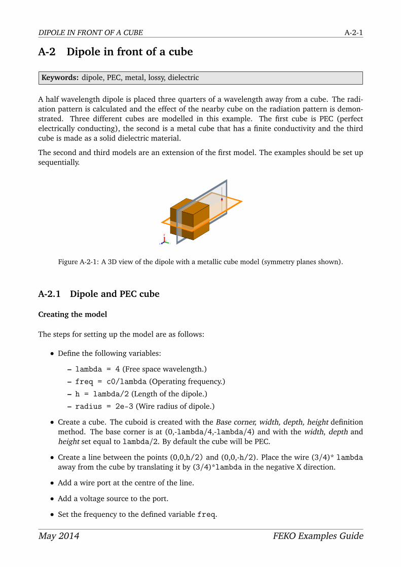
A-2 Dipole in front of a cube
Keywords: dipole, PEC, metal, lossy, dielectric
A half wavelength dipole is placed three quarters of a wavelength away from a cube. The radi-ation pattern is calculated and the effect of the nearby cube on the radiation pattern is demon-strated. Three different cubes are modelled in this example. The first cube is PEC (perfectelectrically conducting), the second is a metal cube that has a finite conductivity and the thirdcube is made as a solid dielectric material.
The second and third models are an extension of the first model. The examples should be set upsequentially.
Figure A-2-1: A 3D view of the dipole with a metallic cube model (symmetry planes shown).
A-2.1 Dipole and PEC cube
Creating the model
The steps for setting up the model are as follows:
• Define the following variables:
– lambda = 4 (Free space wavelength.)
– freq = c0/lambda (Operating frequency.)
– h = lambda/2 (Length of the dipole.)
– radius = 2e-3 (Wire radius of dipole.)
• Create a cube. The cuboid is created with the Base corner, width, depth, height definitionmethod. The base corner is at (0,-lambda/4,-lambda/4) and with the width, depth andheight set equal to lambda/2. By default the cube will be PEC.
• Create a line between the points (0,0,h/2) and (0,0,-h/2). Place the wire (3/4)* lambdaaway from the cube by translating it by (3/4)*lambda in the negative X direction.
• Add a wire port at the centre of the line.
• Add a voltage source to the port.
• Set the frequency to the defined variable freq.
May 2014 FEKO Examples Guide

DIPOLE IN FRONT OF A CUBE A-2-2
Requesting calculations
All electric fields will be tangential to the Y=0 plane, and normal to the Z=0 planes. An electricplane of symmetry is therefore used for the Z=0 plane, and a magnetic plane of symmetry forthe Y=0 plane.
The solution requests are:
• A horizontal radiation pattern cut is calculated to show the distortion of the dipole’s patterndue to the proximity of the cuboid. (0≤φ≤360 with θ=90), with φ=0 where θ andφ denotes the angles theta and phi.
Meshing information
• Use the standard auto-mesh setting.
• Wire segment radius: radius.
CEM validate
After the model has been meshed, run CEM validate. Take note of any warnings and errors.Correct any errors before running the FEKO solution kernel.
A-2.2 Dipole and lossy metal cube
The calculation requests and mesh settings are the same as in the previous model.
Extending the first model
The model is extended with the following steps performed sequentially:
• Create a metallic medium called lossy_metal. Set the conductivity of the metal to 1e2.
• Set the region inside the cuboid to free space.
• Set lossy metal properties on the cuboid faces by right-clicking in the details tree. Set theFace medium to lossy_metal and the thickness to 0.005.
Meshing information
• Use the standard auto-mesh setting.
• Wire segment radius: radius.
May 2014 FEKO Examples Guide
DIPOLE IN FRONT OF A CUBE A-2-3
A-2.3 Dipole and dielectric cube
The calculation requests are the same as in the previous model.
Extending the model
The model is extended with the following steps performed sequentially:
• Create a dielectric medium called diel and relative permittivity of 2.
• Set the region of the cuboid to diel.
• Set the face properties of the cuboid to default. This means that CADFEKO will decide theface medium based on the geometry.
• Delete the lossy_metal metallic medium.
Meshing information
• Use the standard auto-mesh setting.
• Wire segment radius: radius.
CEM validate
After the model has been meshed, run CEM validate. Take note of any warnings, notes anderrors. Please correct error before running the FEKO solution kernel.
A-2.4 Comparison of the results
The gain (in dB) of all three models are shown on a polar plot in Figure A-2-2. We can clearlysee the pronounced scattering effect of the PEC and lossy metal cube with very little differencebetween their results.
We also see that dielectric cube has a very different effect. The dielectric cube results in anincrease in the direction of the cube.
May 2014 FEKO Examples Guide

DIPOLE IN FRONT OF A CUBE A-2-4
-2-101234
0
30
6090
120
150
180
210
240270
300
330
0
Gain
PEC
Lossy Metal
Dielectric
Figure A-2-2: A comparative polar plot of the requested far field gain in dB.
May 2014 FEKO Examples Guide

DIPOLE IN FRONT OF A PLATE A-3-1
A-3 Dipole in front of a plate modelled using MoM, FDTD,UTD, GO and PO
Keywords: MoM, HOBF, UTD, PO, GO, FDTD, dipole, radiation pattern, far field, electricallylarge plate
A dipole in front of an electrically large square plate is considered. This simple example illustrateshow to solve a model using different techniques. First the dipole and the plate is solved with thetraditional MoM. The plate is then modified so that it can be solved with higher order basisfunction MoM, FDTD, UTD, GO and later PO and LE-PO. The MoM/UTD, MoM/GO, MoM/POand MoM/LE-PO hybrid solutions demonstrated here are faster and require fewer resources thanthe traditional MoM solution. When applicable these approximations can be used to greatlyreduce the required solution time and resources required when they are applicable.
Figure A-3-1: A 3D view of the dipole in front of a metallic plate.
A-3.1 Dipole in front of a large plate
Creating the model
The steps for setting up the model are as follows:
• Define the following variables:
– d = 2.25 (Separation distance between dipole and plate. [3*lambda/4])
– h = 1.5 (Length of the dipole. [lambda/2])
– a = 4.5 (Half-side length of plate.)
– rho = 0.006
• The wire dipole is a distance d from the plate in the U axis direction. The dipole is h longand should be centred around the U axis. Create the dipole (line primitive) by entering thefollowing 2 points: (d,0,-h/2), (d,0,h/2).
• Create the plate by first rotating the workplane 90 degrees around the V axis.
May 2014 FEKO Examples Guide

DIPOLE IN FRONT OF A PLATE A-3-2
• Create the rectangle primitive by making use of the following rectangle definition method:Base centre, width, depth. Enter the centre as (0,0,0) and the width = 2*a and depth =2*a.
• Add a segment port on the middle of the wire.
• Add a voltage source to the port. (1 V, 0, 50 Ω)
• Set the total source power (no mismatch) to 1 W.
• Set the frequency to c0/3. We chose lambda as 3 m.
• The model contains symmetry and 2 planes of symmetry may be added to accelerate thesolution. A magnetic plane of symmetry is added on the y=0 plane, and an electric planeof symmetry on the Z=0 plane.
Requesting calculations
The solution requests are:
• Create a horizontal cut of the far field. (0≤φ≤360, θ=90)
Meshing information
Use the standard auto-mesh setting with the wire radius set to rho.
CEM validate
After the model has been meshed, run CEM validate. Take note of any warnings and errors.Correct any errors before running the FEKO solution kernel.
A-3.2 Dipole and a plate using HOBF MoM
Creating the model
The model is identical to the traditional MoM model. The only change that is required is toenable HOBF functions for the solution.
HOBF is activated by navigating to the Solver settings dialog on the Solve/Run ribbon tab andactivating the “Solve with higher order basis functions (HOBF)” check box. Also ensure the basisfunction order is set to auto.
Meshing information
Use the standard auto-mesh setting with the wire radius set to rho. After changing the solu-tion method to use HOBF, the model must be remeshed since HOBF elements are larger thantraditional MoM elements.
May 2014 FEKO Examples Guide
DIPOLE IN FRONT OF A PLATE A-3-3
CEM validate
After the model has been meshed, run CEM validate. Take note of any warnings and errors.Correct any errors before running the FEKO solution kernel.
A-3.3 Dipole and a plate using FDTD
Creating the model
The model is identical to the traditional MoM model. The only change that is required is toenable FDTD by navigating to the Solver settings dialog on the Solve/Run ribbon tab.
Meshing information
Use the standard auto-mesh setting with the wire radius set to rho. After changing the solutionmethod, the model must be remeshed to obtain a voxel mesh representation of the geometry.
CEM validate
After the model has been meshed, run CEM validate. Take note of any warnings and errors.Correct any errors before running the FEKO solution kernel.
A-3.4 Dipole and a UTD plate
Creating the model
The model is identical to the MoM model. The only change that is required is that the solutionmethod to be used on the plate must be changed.
This change is made by going to the face properties of the plate in the detail tree of CADFEKO. Onthe solution tab use the dropdown box named Solve with special solution method and choosingUniform theory of diffraction (UTD). Now when meshing is done in CADFEKO the plate will notbe meshed into triangular elements.
Remove the symmetry definitions for the UTD example - the number of elements is so small thatit is faster to simulate without symmetry.
Meshing information
Use the standard auto-mesh setting with the wire radius set to rho. After changing the solutionmethod on the plate to UTD, the model must be remeshed. UTD plates are not meshed and asingle element will be created for the entire plate.
May 2014 FEKO Examples Guide

DIPOLE IN FRONT OF A PLATE A-3-4
CEM validate
After the model has been meshed, run CEM validate. Take note of any warnings and errors.Correct any errors before running the FEKO solution kernel.
A-3.5 Dipole and a GO plate
Creating the model
The model is identical to the MoM model (note that we are changing the MoM model and notthe UTD model). The only change that is required is that the solution method to be used on theplate must be changed.
This change is made by going to the face properties of the plate in the detail tree of CADFEKO. Onthe solution tab use the dropdown box named Solve with special solution method and choosingGeometrical optics (GO) - ray launching.
Meshing information
Use the standard auto-mesh setting with the wire radius set to rho. After changing the solutionmethod on the plate to GO, the model must be remeshed. The triangle sizes are determined bythe geometrical shape and not the operating wavelength. Unlike the UTD plate, the plate will bemeshed into triangular elements for the GO.
CEM validate
After the model has been meshed, run CEM validate. Take note of any warnings and errors.Correct any errors before running the FEKO solution kernel.
A-3.6 Dipole and a PO plate
Creating the model
The model is identical to the MoM model. The only change that is required is that the solutionmethod to be used on the plate must be changed.
This change is made by going to the face properties of the plate in the detail tree of CADFEKO. Onthe solution tab use the dropdown box named Solve with special solution method and choosingPhysical optics (PO) - always illuminated. The ‘always illuminated’ option may be used in thiscase, as it is clear that there will be no shadowing effects in the model. With this option, the ray-tracing required for the physical optics solution can be avoided thereby accelerating the solution.
Meshing information
Use the standard auto-mesh setting with the wire radius set to rho. The auto-mesh feature takesthe solution method into account.
May 2014 FEKO Examples Guide

DIPOLE IN FRONT OF A PLATE A-3-5
CEM validate
After the model has been meshed, run CEM validate. Take note of any warnings and errors.Correct any errors before running the FEKO solution kernel.
A-3.7 Comparative results
The total far field gain of the dipole in front of the PEC plate is shown on a dB polar plot inFigure A-3-2. The MoM/UTD, MoM/PO and full MoM reference solution are shown. To obtainthe large element PO (LE-PO) models, set the solution method from Physical optics (PO) - al-ways illuminated to Large element physical optics (LE-PO) - always illuminated and save the POexample files under a new name. Since the dipole is less than a wavelength away from the plate,the standard auto-meshing will not work. Mesh the plate with a triangle edge length of a/4.
-30
-20
-10
0
10
0
30
6090
120
150
180
210
240270
300
330
0
Far field
MoM & GOMoM (HOBF)MoM & LEPOMoM (traditional RWG)MoM & POMoM & UTDFDTD
Figure A-3-2: A polar plot of the total far field gain (dB) computed in the horizontal plane using theMoM/GO, MoM/UTD, MoM/PO, MoM/LE-PO and FDTD methods compared to the full MoM(traditional and HOBF) reference solution.
The comparison between memory requirements and runtimes are shown in Table A-3-1. Themethod of moments (MoM) is used as reference and all other methods are compared using amemory and runtime factor. Requirements for the MoM solution was 10 s and 51.88 MB.
May 2014 FEKO Examples Guide

DIPOLE IN FRONT OF A PLATE A-3-6
Solution method Memory (% of MoM) Runtime (% of MoM)
MoM (HOBF - auto) 4.88 140Physical optics: MoM/PO 2.23 6Large element PO: MoM/LE-PO 0.29 1.47Uniform theory of diffraction: MoM/UTD 0.08 1.32Geometric optics: MoM/GO 1.28 4.23FDTD 101.23 1310
Table A-3-1: Comparison of resource requirements for the model using different solver techniques.
May 2014 FEKO Examples Guide

A MONOPOLE ANTENNA ON A FINITE GROUND PLANE A-4-1
A-4 A monopole antenna on a finite ground plane
Keywords: monopole, finite ground, radiation pattern, far field, current
A quarter wave monopole antenna on a finite circular ground plane is constructed and simulated.The circular ground has a circumference of three wavelengths, and the wire has a radius of 1 mm.The operating frequency is 75 MHz.
Figure A-4-1: A 3D view of the monopole on a finite circular ground (symmetry planes shown).
A-4.1 Monopole on a finite ground
Creating the model
The steps for setting up the model are as follows:
• Define the following variables:
– freq = 75e6 (Operating frequency.)
– lambda = c0/freq (Free space wavelength.)
– R = 3*lambda/(2*pi) (Radius of the ground plane.)
– wireRadius = 1e-3 (Radius of the monopole wire segments.)
• Create the ground using the ellipse primitive. Set the radii equal to the defined variable Rand the label to ground.
• Create a line between (0,0,0) and (0,0,lambda/4) and rename as monopole.
• Union the wire and the ground.
• Add a wire vertex port on the line. The port preview should show the port located at thejunction between the wire and the ground plane. If this is not so, change the port positionbetween Start and End.
• Add a voltage source to the port. (1 V, 0, 50 Ω)
• Set the frequency equal to freq.
May 2014 FEKO Examples Guide
A MONOPOLE ANTENNA ON A FINITE GROUND PLANE A-4-2
Requesting calculations
Two planes of magnetic symmetry are defined at the x = 0 plane and the y = 0 plane.
The solution requests are:
• A full 3D far field pattern with 2 increments.
• All currents are saved to allow viewing in POSTFEKO.
Meshing information
• Use the standard auto-mesh setting.
• Wire segment radius: wireRadius.
CEM validate
After the model has been meshed, run CEM validate.
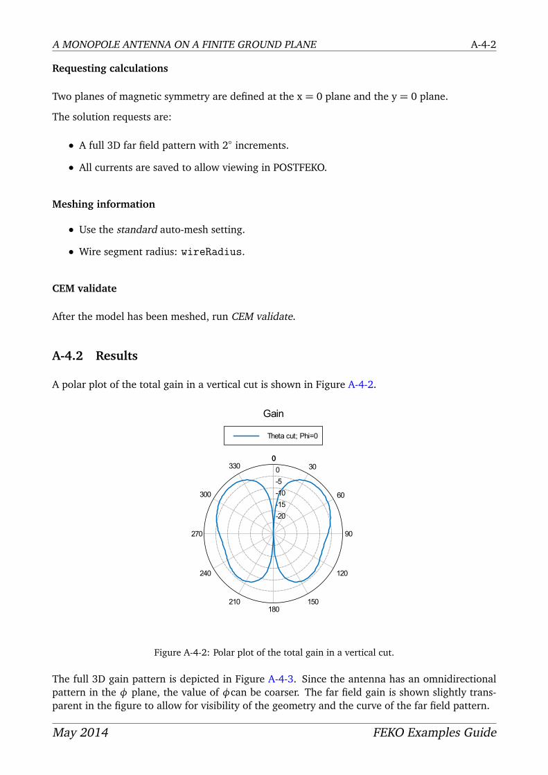
A-4.2 Results
A polar plot of the total gain in a vertical cut is shown in Figure A-4-2.
-20-15-10-50
030
60
90
120
150180
210
240
270
300
3300
Gain
Theta cut; Phi=0
Figure A-4-2: Polar plot of the total gain in a vertical cut.
The full 3D gain pattern is depicted in Figure A-4-3. Since the antenna has an omnidirectionalpattern in the φ plane, the value of φcan be coarser. The far field gain is shown slightly trans-parent in the figure to allow for visibility of the geometry and the curve of the far field pattern.
May 2014 FEKO Examples Guide

A MONOPOLE ANTENNA ON A FINITE GROUND PLANE A-4-3
Figure A-4-3: A full 3D plot of the antenna gain.
The currents on all elements (wire segment and surface triangles) are shown in Figure A-4-4. Thecurrents are indicated by the geometry colouring based on the legend colour scale. This allowsidentification of points where the current is concentrated. The surface currents are displayed indecibels.
The phase evolution of the current display may be animated (as with many other results displaysin POSTFEKO) on the Animate tab on the ribbon.
Figure A-4-4: 3D view of the current on the ground plane of the monopole antenna.
May 2014 FEKO Examples Guide

YAGI-UDA ANTENNA ABOVE A REAL GROUND A-5-1
A-5 Yagi-Uda antenna above a real ground
Keywords: antenna, Yagi-Uda antenna, real ground, infinite planar Green’s function, optimi-sation
In this example we consider the radiation of a horizontally polarised Yagi-Uda antenna consistingof a dipole, a reflector and three directors. The frequency is 400 MHz. The antenna is located3 m above a real ground which is modelled with the Green’s function formulation.
Note that the model provided with this example includes a basic optimisation. The optimisationis set up such that the optimal dimensions of the antenna may be determined to achieve a specificgain pattern (maximise the forward gain and minimise back lobes).
Figure A-5-1: A 3D view of the Yagi-Uda antenna suspended over a real ground.
A-5.1 Antenna and ground plane
Creating the model
The steps for setting up the model are as follows:
• Define the following variables:
– freq = 400e6 (Operating frequency.)
– lambda = c0/freq (The wavelength in free space at the operating frequency.)
– lr = 0.477*lambda (Length of the reflector.)
– li = 0.451*lambda (Length of the active element.)
– ld = 0.442*lambda (Length of the directors.)
– d = 0.25*lambda (Spacing between elements.)
– h = 3 (Height of the antenna above ground.)
– epsr = 10 (Relative permittivity of the ground.)
May 2014 FEKO Examples Guide

YAGI-UDA ANTENNA ABOVE A REAL GROUND A-5-2
– sigma = 1e-3 (Ground conductivity.)
– wireRadius = 1e-3 (Wire radius (1 mm).)
• Create the active element with start point as (0, -li/2, h) and the end point as (0, li/2,h). Set the label as activeElement.
• Add a vertex port in the centre of the wire.
• Add a voltage source on the port. (1 V, 0, 50 Ω)
• Create the wire for the reflector. Set the Start point as (-d, -lr/2, h) and the End point as(-d, lr/2, h). Set the label as reflector.
• Create the three wires for the directors.
Director Start point End point
director1 (d, -ld/2, h) (d, ld/2, h)director2 (2*d, -ld/2, h) (2*d, ld/2, h)director3 (3*d, -ld/2, h) (3*d, ld/2, h)
• Create a dielectric called ground with relative permittivity of epsr and conductivity equalto sigma.
• Set the lower half space to ground. This can be done by setting the infinite plane to usethe exact Sommerfeld integrals.
• Set the frequency to freq.
Requesting calculations
A single plane of electrical symmetry on the Y=0 plane is used in the solution of this problem.
The solution requests are:
• Create a vertical far field request above the ground plane. (-90≤θ≤90, with φ=0 andθ=0.5 increments)
• Set the Workplane origin of the far field request to (0, 0, 3).
Meshing information
Use the standard auto-meshing option with the wire segment radius equal to wireRadius.
May 2014 FEKO Examples Guide

YAGI-UDA ANTENNA ABOVE A REAL GROUND A-5-3
CEM validate
After the model has been meshed, run CEM validate. Take note of any warnings and errors.Correct any errors before running the FEKO solution kernel.
Note that a warning may be encountered when running the solution. This is because lossescannot be calculated in an infinitely large medium, as is required for the extraction of antennadirectivity information (gain is computed by default). This warning can be avoided by ensuringthat the far field gain be calculated instead of the directivity. This is set on the Advanced tab ofthe far field request in the tree.
A-5.2 Results
The radiation pattern is calculated in the H plane of the antenna. A simulation without theground plane is compared with the results from the model provided for this example in Fig-ure A-5-2. As expected, the ground plane greatly influences the radiation pattern. (Note that thegraph is a vertical polar plot of the gain in dB for the two cases.)
-20
-10
0
10
030
60
90
120
150180
210
240
270
300
3300
Far field
No Ground
Real Ground
Real Ground (Optimised)
Figure A-5-2: The directivity pattern of the Yagi-Uda antenna over a real ground and without any ground.Note that the optimised pattern is also shown.
May 2014 FEKO Examples Guide

PATTERN OPTIMISATION OF A YAGI-UDA ANTENNA A-6-1
A-6 Pattern optimisation of a Yagi-Uda antenna
Keywords: antenna, Yagi-Uda, radiation pattern, optimisation
In this example we consider the optimisation of a Yagi-Uda antenna (consisting of a dipole, areflector and two directors) to achieve a specific radiation pattern and gain requirement. Thefrequency is 1 GHz. The antenna has been roughly designed from basic formulae, but we wouldlike to optimise the antenna radiation pattern such that the gain is above 8 dB in the main lobe(-30 ≤ φ≤ 30) and below -7 dB in the back lobe (90 ≤ φ≤ 270).
Figure A-6-1: A 3D view of the Yagi-Uda antenna.
A-6.1 The antenna
Creating the model
The steps for setting up the model are as follows:
• Define the following variables (physical dimensions based on initial rough design):
– freq = 1e9 (The operating frequency.)
– lambda = c0/freq (The wavelength in free space at the operating frequency.)
– L0 = 0.2375 (Length of one arm of the reflector element in wavelengths.)
– L1 = 0.2265 (Length of one arm of the driven element in wavelengths.)
– L2 = 0.2230 (Length of one arm of the first director in wavelengths.)
– L3 = 0.2230 (Length of one arm of the second director in wavelengths.)
– S0 = 0.3 (Spacing between the reflector and driven element in wavelengths.)
– S1 = 0.3 (Spacing between the driven element and the first director in wavelengths.)
– S2 = 0.3 (Spacing between the two directors in wavelengths.)
– r = 1e-4 (Radius of the elements.)
• Create the active element of the Yagi-Uda antenna. Set the start point as (0, 0, -L1*lambda)and the end point as (0, 0, L1*lambda).
• Add a port on a segment in the centre of the wire.
• Add a voltage source on the port. (1 V, 0, 50 Ω)
May 2014 FEKO Examples Guide

PATTERN OPTIMISATION OF A YAGI-UDA ANTENNA A-6-2
• Set the incident power for a 50 Ω transmission line to 1 W.
• Create the wire for the reflector. Set the start point as (-S0*lambda, 0, -L0*lambda) andthe end point as (-S0*lambda, 0, L0*lambda).
• Create the two directors:
– Set the start point and end point for director1 as the following: (S1*lambda, 0,-L2*lambda) and (S1*lambda, 0, L2*lambda), respectively.
– For director2, set the start point as ((S1 + S2)*lambda, 0, -L3*lambda) and theend point ((S1 + S2)*lambda, 0, L3*lambda).
• Set the frequency to freq.
Requesting calculations
The Z=0 plane is an electric plane of symmetry.
A magnetic plane of symmetry exists in the Y=0 plane, but since all the wires are in the Y=0plane, adding the magnetic symmetry setting would not affect the simulation speed and can beneglected.
The solution requests are:
• Create a horizontal far field request labelled ‘H_plane’. (0≤φ≤180, θ=90 and 2 incre-ments)
Meshing information
Use the standard auto-mesh setting with the wire segment radius equal to r.
Setting up optimisation
• An optimisation search is added with the Simplex method and Low accuracy.
• The following parameters are set:
– L0 (min 0.15; max 0.35; start 0.2375)
– L1 (min 0.15; max 0.35; start 0.2265)
– L2 (min 0.15; max 0.35; start 0.22)
– L3 (min 0.15; max 0.35; start 0.22)
– S0 (min 0.1; max 0.32; start 0.3)
– S1 (min 0.1; max 0.32; start 0.3)
– S2 (min 0.1; max 0.32; start 0.3)
• For this example, it is required that the reflector element be longer than all the directorelements. The following constraints are therefore also defined:
May 2014 FEKO Examples Guide

PATTERN OPTIMISATION OF A YAGI-UDA ANTENNA A-6-3
– L2 < L0
– L3 < L0
• Two optimisation masks are created (see figure A-6-2. The first mask (Mask_max) definesthe upper limit of the required gain (gain < 15 between 0 and 88; gain < -7 between 90
and 180). The purpose of this mask is to define the region that defines the upper boundary.The value of 15 dB in the forward direction was chosen arbitrarily high knowing that thisantenna will not be able to achieve 15 dB gain and thus does not have an affect on theoptimisation. Upper limit of -7 dB from 90 to 180 will have an effect on the optimisationand determines the size of the back lobes that we are willing to accept.
• The second Mask (Mask_min) defines the lower limit of the required gain (gain > 8 dBbetween 0 and 30; gain > -40 dB between 32 and 180). This mask is used to determinethe desired main lobe gain. The value of -40 dB outside the main lobe was chosen arbitrarilylow and thus will not affect the optimisation.
• Two far field optimisation goals are added based on the H_plane calculation request. ThedB values (10 ∗ log[]) of the vertically polarised gain at all angles in the requested rangeis required to be greater than Mask_min and less than Mask_max.
A weighting for both goals are equal since neither of the goals are more important than the other.The weighting that should be used depends on the goal of the optimisation.
A-6.2 Results
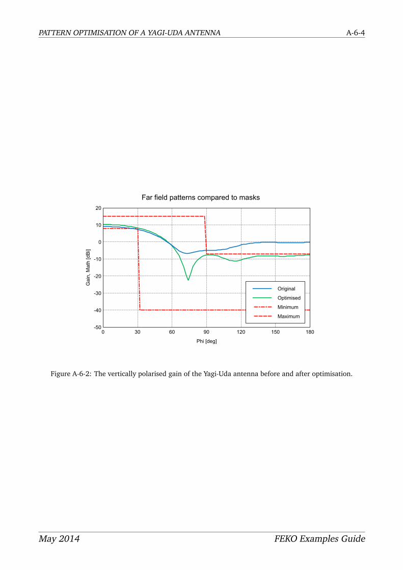
The radiation pattern (calculated in the E plane of the antenna) is shown in Figure A-6-2 forboth the initial design and the antenna resultant after the optimisation process. The gain in theback-lobe region (between 90 and 180 degrees) has been reduced to around -7dB, while the gainover the main-lobe region (between 0 and 30 degrees) is above 8dB. (Note that the graph showsthe vertically polarised gain plotted in dB with respect to φ.)
The extract below from the optimisation log file, indicates the optimum parameter values foundduring the optimisation search:
=============== SIMPLEX NELDER-MEAD: Finished ===============
Optimisation finished (Goal reached: 0.000000000e+00)
Optimum found for these parameters:l0 = 2.444318132e-01l1 = 2.027415724e-01l2 = 2.316878577e-01l3 = 2.214280613e-01s0 = 2.636975325e-01s1 = 2.346861767e-01s2 = 3.165823417e-01
Optimum aim function value (at no. 79): 0.000000000e+00No. of the last analysis: 79
May 2014 FEKO Examples Guide
PATTERN OPTIMISATION OF A YAGI-UDA ANTENNA A-6-4
-50
-40
-30
-20
-10
0
10
20
0 30 60 90 120 150 180
Gai
n, M
ath
[dBi
]
Phi [deg]
Far field patterns compared to masks
Original
Optimised
Minimum
Maximum
Figure A-6-2: The vertically polarised gain of the Yagi-Uda antenna before and after optimisation.
May 2014 FEKO Examples Guide

LOG PERIODIC ANTENNA A-7-1
A-7 Log periodic antenna
Keywords: Transmission line, dipole, array, far field
A log periodic example uses the non-radiating transmission lines to model the boom of a logperiodic dipole array antenna. The antenna is designed to operate around 46.29 MHz, with anoperational bandwidth over a wide frequency range (35 MHz to 60 MHz).
Figure A-7-1 shows the log periodic dipole array (LPDA) with a transmission line feed network.
Figure A-7-1: The model of LPDA using transmission lines to model the boom structure.
A-7.1 Log periodic dipole array
Creating the model
The steps for setting up the model are as follows:
• Create the variables required for the model.
– freq = 46.29e6 (The operating frequency.)
– tau = 0.93 (The growth factor.)
– sigma0 = 0.7 (Spacing)
– len0 = 2 (Length of the first element.)
– d0 = 0 (Position of the first element.)
– rad0 = 0.00667 (Radius of the first element.)
– sigma1. . .sigma11: sigmaN = sigma(N-1)/tau
– d1. . .d11: dN = d(N-1) – sigmaN
– len1. . .len11: lenN = len(N-1)/tau
– rad1. . .rad11: radN = rad(N-1)/tau
May 2014 FEKO Examples Guide

LOG PERIODIC ANTENNA A-7-2
– lambda = c0/freq (Free space wavelength.)
– Zline = 50 (Transmission line impedance.)
– Zload = 50 (Shunt load resistance.)
• Create the twelve dipoles using the defined variables. Create line (geometry) number Nfrom (dN,-lenN/2,0) to (dN,lenN/2,0). For example, to create dipole 1, create a linefrom (d1,-len1/2,0) to (d1,len1/2,0).
• Add a port in the centre of every dipole.
• Define eleven transmission lines to connect the dipoles. Each transmission line has a char-acteristic impedance of Zline (real part of Z0 (Ohm)) and a transmission line length ofsigmaN. Check the Cross input and output ports to ensure correct orientation of the trans-mission line connections.
• For each segment set the local wire radius equal to the defined radN variable.
• Connect transmission line N between port(N-1) and portN for all of the transmissionlines, see Figure A-7-2.
• Define the shunt load using the admittance definition of a general non-radiating network(Y-parameter). Specify the one-port admittance matrix manually (Y11 = 1/Zload).
• Connect the general network to the final port (i.e. the port of the longest dipole element).
• Set the continuous (interpolated) frequency range from 35 MHz to 60M MHz.
• Add a voltage source to the port at the first dipole at the origin.
Note that it will be required to connect all of the ports, transmission lines and the networktogether in the schematic view.
Figure A-7-2: The network schematic view showing the connected transmission lines, general networksand ports.
Requesting calculations
Electric symmetry may be applied to the plane at y=0.
A far field pattern is requested in the vertical plane (-180≤θ≤180, with φ=0 and 2 incre-ments).
May 2014 FEKO Examples Guide

LOG PERIODIC ANTENNA A-7-3
Meshing information
Use the standard auto-mesh setting with wire segment radius equal to 0.01. Note that all wireshave local radii set to radN.
CEM validate
After the model has been meshed, run CEM validate. Take note of any warnings and errors.Correct any errors before running the FEKO solution kernel.
Save the file and run the solver.
A-7.2 Results
The vertical gain (in dB) at 46.29 MHz and the input impedance over the operating band of theLPDA are shown in Figure A-7-3 and Figure A-7-4 respectively.
-30
-20
-10
0
10
030
60
90
120
150180
210
240
270
300
3300
Far field gain
Figure A-7-3: The vertical gain of a LPDA antenna at 46.29 MHz.
May 2014 FEKO Examples Guide

LOG PERIODIC ANTENNA A-7-4
-20
-10
0
10
20
30
40
50
60
35 40 45 50 55 60
Impe
danc
e [O
hm]
Frequency [MHz]
Real
Imaginary
Figure A-7-4: The input impedance (real and imaginary) of the LPDA antenna over the operating band.
May 2014 FEKO Examples Guide

MICROSTRIP PATCH ANTENNA A-8-1
A-8 Microstrip patch antenna
Keywords: microstrip, patch antenna, dielectric substrate, pin feed, edge feed, optimisation,SEP, FDTD
A microstrip patch antenna is modelled using different feed methods. The dielectric substrate ismodelled as a finite substrate and ground using the surface equivalence principle (SEP) as well asa planar multilayer substrate with a bottom ground layer (using a special Green’s function). Thesimulation time and resource requirements are greatly reduced using an infinite plane, althoughthe model may be less representative of the physical antenna. The two different feeding methodsconsidered are a pin feed and a microstrip edge feed.
In this example, each model builds on the previous one. It is recommended the models be builtand considered in the order they are presented. If you would like to build and keep the differentmodels, start each model by saving the model to a new location.
Note that the model provided with this example for the pin-fed patch (SEP) on a finite substrateincludes a basic optimisation set up. The optimisation is defined to determine the value for thepin offset which gives the best impedance match to a 50 Ω system.
A-8.1 Pin-fed, SEP model
Creating the model
In the first example a feed pin is used and the substrate is modelled with a dielectric with specifieddimensions. The geometry of this model is shown in Figure A-8-1.
Figure A-8-1: A 3D representation of a pin fed microstrip patch antenna on a finite ground.
The steps for setting up the model are as follows: (Note that length is defined in the direction ofthe X axis and width in the direction of the Y axis.)
• Set the model unit to millimetres.
• Define the following variables (physical dimensions based on initial rough design):
– epsr = 2.2 (The relative permittivity of the substrate.)
– freq = 3e9 (The centre frequency.)
– lambda = c0/freq*1e3 (The wavelength in free space.)
– lengthX = 31.1807 (The length of the patch in the X direction.)
May 2014 FEKO Examples Guide

MICROSTRIP PATCH ANTENNA A-8-2
– lengthY = 46.7480 (The length of the patch in the Y direction.)
– offsetX = 8.9 (The location of the feed.)
– substrateLengthX = 50 (The length of the substrate in the X direction.)
– substrateLengthY = 80 (The length of the substrate in the Y direction.)
– substrateHeight = 2.87 (The height of the substrate.)
– fmin = 2.7e9 (The minimum frequency in the simulation range.)
– fmax = 3.3e9 (The maximum frequency in the simulation range.)
– feedlineWidth = 4.5 (The width of the feedline for the microstrip model feed.)
• Create the patch by creating a rectangle with the base centre, width, depth definitionmethod. Set the width to the defined variable lengthX and depth equal to lengthY.Rename this label to patch.
• Create the substrate by defining a cuboid with the base corner, width, depth, height defini-tion method. Set the Base corner to (-substrateLengthX/2, -substrateLengthY/2, -substrateHeight), width = substrateLengthX, depth = substrateLengthY, height= substrateHeight). Rename this label to substrate.
• Create the feed pin as a wire between the patch and the bottom of the substrate positioned8.9 mm (offsetX) from the edge of the patch. The pin’s offset is in the X direction andshould have no offset in the Y direction.
• Add a segment wire port on the middle of the wire.
• Add a voltage source on the port. (1 V, 0, 50 Ω)
• Union all the elements and label the union antenna.
• Create a new dielectric called substrate with relative permittivity equal to epsr.
• Set region of the cube to substrate.
• Set the faces representing the patch and the ground below the substrate to PEC.
• Set a continuous frequency range from fmin to fmax.
Requesting calculations
A single plane of magnetic symmetry is used on the Y=0 plane.
The solution requests are:
• Create a vertical (E plane) far field request. (-90≤θ≤90, with φ=0 and 2 increments)
• Create a vertical (H plane) far field request. (-90≤θ≤90, with φ=90 and 2 increments)
Meshing information
Use the standard auto-mesh setting with the wire segment radius equal to 0.25.
May 2014 FEKO Examples Guide

MICROSTRIP PATCH ANTENNA A-8-3
CEM validate
After the model has been meshed, run CEM validate.
A-8.2 Pin-fed, FDTD model
Creating the model
The model is now solved by means of the FDTD solver. It is still pin-fed as in the previousexample.
Figure A-8-2: A 3D representation of a pin fed microstrip patch antenna on a finite ground.
The model is extended with the following steps performed sequentially:
• Activate the finite difference time domain (FDTD) solver.
• Change the continuous frequency range to linearly spaced discrete points ranging fromfmin to fmax with the number of frequencies set to 51.
• Define the boundary condition settings. Set the Top (Z+), -Y, +Y, -X and +X boundaries toOpen and Automatically add a free space buffer. Set the Bottom (Z-) boundary to Perfectelectric conductor (PEC) and Do not add a free space buffer.
Meshing information
Use the standard auto-mesh setting with the wire segment radius equal to 0.25.
CEM validate
After the model has been meshed, run CEM validate.
A-8.3 Pin-fed, planar multilayer substrate
Creating the model
This model is an extensions of the first model. The substrate is now modelled with a planarmultilayer substrate (Green’s functions). It is still pin-fed as in the previous two examples.
The model is extended with the following steps performed sequentially:
May 2014 FEKO Examples Guide

MICROSTRIP PATCH ANTENNA A-8-4
Figure A-8-3: A 3D representation of a pin fed microstrip patch antenna on an infinite ground.
• Delete the substrate component from the antenna geometry.
• Add a voltage source on the port. (1 V, 0, 50 Ω)
• Add a planar multilayer substrate (infinite plane) with a conducting layer at the bottom.Layer1 must be set to substrate with a height of substrateHeight.
The meshing values can remain unchanged, as the values used for the previous simulation aresufficient. Run CEM validate.
Note that a warning may be encountered when running the solution. This is because lossescannot be calculated in an infinitely large medium, as is required for the extraction of antennadirectivity information (gain is computed by default). This warning can be avoided by ensuringthat the far field gain be calculated instead of the directivity. This is set on the advanced tab ofthe far field request in the tree.
A-8.4 Edge-fed, planar multilayer substrate
Creating the model
This fourth model is an extension of the third model. The patch is now edge fed and the mi-crostrip feed is used.
NOTE: This example is only for the purposes of demonstration. Usually, the feed line is insertedto improve the impedance match. Also, for improved accuracy the edge source width (here thewidth of the line of 4.5 mm) should not be wider than 1/30 of a wavelength. This means thatstrictly speaking the microstrip port should not be wider than about 3 mm.
Figure A-8-4: A 3D representation of an edge fed microstrip patch antenna on an infinite ground.
The modification is as follows:
• Copy the patch from the antenna.
• Delete the antenna geometry so that only the patch remains.
May 2014 FEKO Examples Guide

MICROSTRIP PATCH ANTENNA A-8-5
• Create a rectangle using the base corner, width, depth method, with the base corner at(-lengthX/2,-feedlineWidth/2,0). The width of the line should be -lambda/4 and thedepth should be feedlineWidth. Label the part feedline.
• Union all the elements.
• Add a microstrip port at the edge of the feed line.
• Add a voltage source on the port. (1 V, 0, 50 Ω).
All meshing and calculation requests can remain the same as in the previous example. Run theCEM validate.
A-8.5 Comparison of the results for the different models
The far field gain patterns for all 4 antenna models at 3 GHz are plotted on the same graph inFigure A-8-5. The model with the finite ground should be the best representation of an antennathat can physically be manufactured, but the simulation time compared to the infinite planesolution is considerably longer. We can also see how the different feeding mechanisms impactthe radiation pattern.
-15
-10
-5
0
5
030
60
90
120
150180
210
240
270
300
3300
Pin feed (finite ground) [MoM]
Pin feed (infinite ground) [MoM]
Mircostip feed (infinite ground) [MoM]
Pin feed (finite ground) [FDTD]
Figure A-8-5: The E plane radiation pattern of the three microstrip patch models.
May 2014 FEKO Examples Guide

PROXIMITY COUPLED PATCH ANTENNA WITH MICROSTRIP FEED A-9-1
A-9 Proximity coupled patch antenna with microstrip feed
Keywords: patch antenna, aperture coupling, microstrip feed, proximity coupling, voltage onan edge, infinite substrate
This example considers a proximity coupled circular patch antenna from 2.8 GHz to 3.2 GHz.The meshed geometry is shown in Figure A-9-1. The feed line of the patch is between the patchand the ground plane.
Figure A-9-1: Proximity coupled circular patch antenna. The lighter triangles are on a lower level (closerto the ground plane).
A-9.1 Circular patch
Creating the model
The steps for setting up the model are as follows:
• Set the model unit to millimetres.
• Define the following variables:
– epsr = 2.62 (The relative permittivity.)
– patch_rad = 17.5 (The patch radius.)
– line_len = 79 (The strip line length.)
– line_width = 4.373 (The strip line width.)
– offset = 0 (Feed line offset from the patch centre.)
– substrate_d = 3.18 (The substrate thickness.)
– f_min = 2.8e9 (The lowest simulation frequency.)
– f_max = 3.2e9 (The highest simulation frequency.)
• Create a new dielectric medium called substrate with relative permittivity of epsr anddielectric loss tangent of 0.
• Create a circular metallic disk with centre of the disc at the origin with radius= patch_rad.
• Create a rectangle with the definition method: Base corner, width, depth. Set the Base cor-ner as the following: (-line_width/2, 0, -substrate_d/2). Set the width= line_widthand depth = line_len.
May 2014 FEKO Examples Guide

PROXIMITY COUPLED PATCH ANTENNA WITH MICROSTRIP FEED A-9-2
• Add a planar multilayer substrate. The substrate is substrate_d thick and is of substratematerial type with a bottom ground plane. Layer0 is of type free space.
• Create a microstrip port on the edge of the feed line furthest away from the patch element.
• Add a voltage source to the port.
• Request that the continuous frequency range is calculated from f_min to f_max.
Meshing information
A single plane of magnetic symmetry is used on the X=0 plane.
Use the standard auto-mesh setting, but play around with the curvature refinement options onthe advanced tab of the mesh dialog. While changing these settings around, create the mesh andinvestigate the effects of the different settings. Also investigate the difference in the results - thisillustrates the importance of performing a mesh conversion test for your model.
No calculation requests are required for this model since the input impedance is available whena voltage excitation has been defined.
CEM validate
After the model has been meshed, run CEM validate. Take note of any warnings and errors.Correct any errors before running the FEKO solution kernel.
A-9.2 Results
Figure A-9-2 shows the reflection coefficient on the Smith chart.
May 2014 FEKO Examples Guide

PROXIMITY COUPLED PATCH ANTENNA WITH MICROSTRIP FEED A-9-3
-10
-5
-3
-2
-1.4-1-0.7
-0.5-0.4
-0.3
-0.2
-0.1
0.1
0.2
0.3
0.40.5
0.7 1 1.4
2
3
5
10
0.1
0.2
0.3
0.4
0.5
0.7 1
1.4 2 3 5 10
Reflection coefficient
Figure A-9-2: Reflection coefficient of the proximity coupled patch.
May 2014 FEKO Examples Guide
MODELLING AN APERTURE COUPLED PATCH ANTENNA A-10-1
A-10 Modelling an aperture coupled patch antenna
Keywords: aperture triangles, infinite planes, SEP
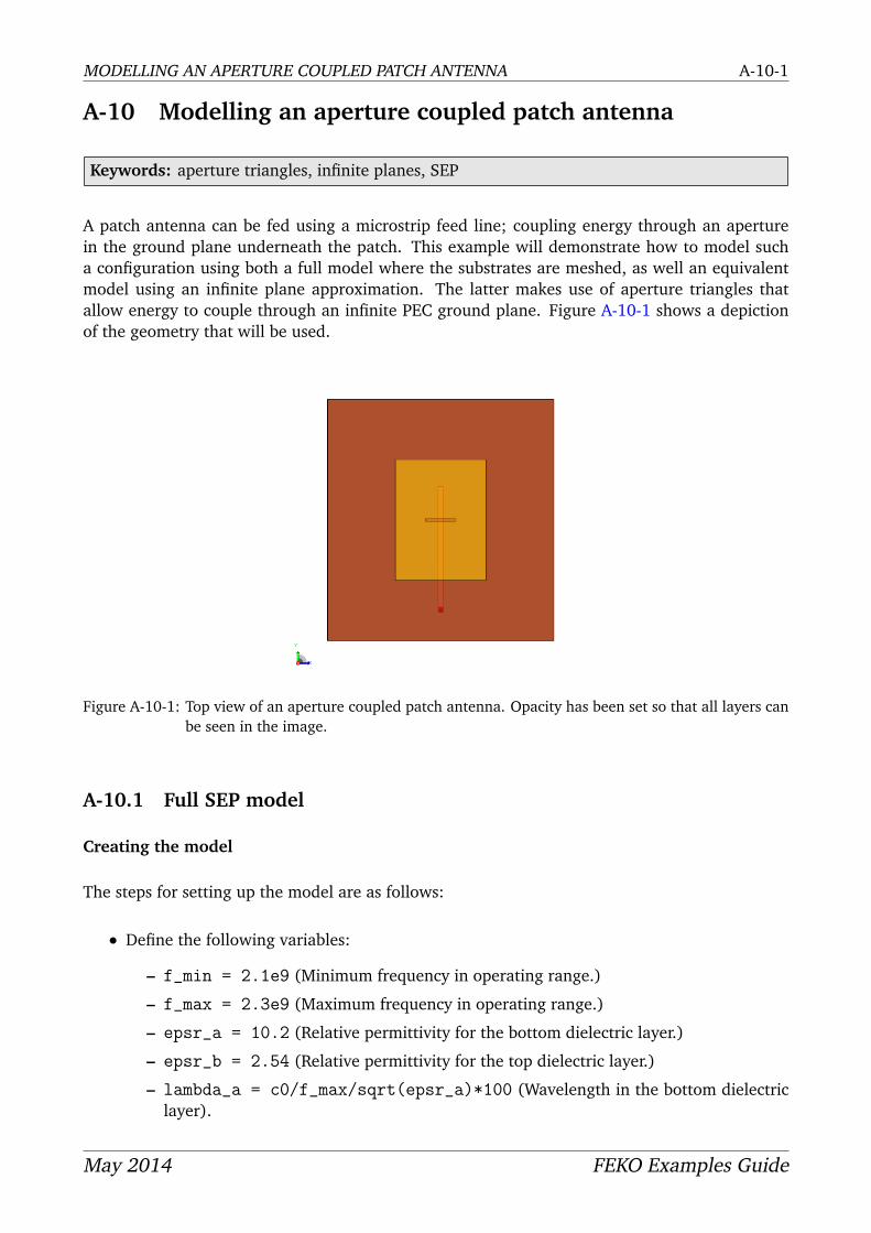
A patch antenna can be fed using a microstrip feed line; coupling energy through an aperturein the ground plane underneath the patch. This example will demonstrate how to model sucha configuration using both a full model where the substrates are meshed, as well an equivalentmodel using an infinite plane approximation. The latter makes use of aperture triangles thatallow energy to couple through an infinite PEC ground plane. Figure A-10-1 shows a depictionof the geometry that will be used.
Figure A-10-1: Top view of an aperture coupled patch antenna. Opacity has been set so that all layers canbe seen in the image.
A-10.1 Full SEP model
Creating the model
The steps for setting up the model are as follows:
• Define the following variables:
– f_min = 2.1e9 (Minimum frequency in operating range.)
– f_max = 2.3e9 (Maximum frequency in operating range.)
– epsr_a = 10.2 (Relative permittivity for the bottom dielectric layer.)
– epsr_b = 2.54 (Relative permittivity for the top dielectric layer.)
– lambda_a = c0/f_max/sqrt(epsr_a)*100 (Wavelength in the bottom dielectriclayer).
May 2014 FEKO Examples Guide

MODELLING AN APERTURE COUPLED PATCH ANTENNA A-10-2
– lambda_b = c0/f_max/sqrt(epsr_b)*100 (Wavelength in top dielectric layer).
– d_a = 0.16 (Height of bottom dielectric layer.)
– d_b = 0.16 (Height of top dielectric layer.)
– patch_l = 4.0 (Length of the patch antenna.)
– patch_w = 3.0 (Width of the patch antenna.)
– grnd_l = 2*patch_l (Length of substrate layers and ground plane.)
– grnd_w = 2.5*patch_w (Width of substrate layers and ground plane.)
– feed_l = lambda_a (Length of the microstrip feed line.)
– feed_w = 0.173 (Width of the microstrip feed line.)
– stub_l = 1.108 (Length of the matching stub on the microstrip feed line.)
– ap_l = 1.0 (Length of the aperture.)
– ap_w = 0.11 (Width of the aperture.)
• Set the model units to centimetres.
• Create a dielectric medium called bottom_layer with relative permittivity of epsr_a anda loss tangent of 0.
• Create a dielectric medium called top_layer with relative permittivity of epsr_b and aloss tangent of 0.
• Create a ground layer using a plate with its centre at (0, 0, 0), a width of grnd_w and adepth of grnd_l. Label the plate ground.
• Create the aperture using a plate with its centre at (0, 0, 0), a width of ap_l and a depthof ap_w. Label the plate aperture.
• Subtract aperture from ground. Note that the ground plane remains, but with a hole inthe centre where the aperture plate was defined. Rename this to slotted_ground.
• Create the patch antenna using a plate with its centre at (0, 0, d_b), a width of patch_wand a depth of patch_l. Label the plate patch.
• Create the microstrip feed line using a plate with a base corner at (-feed_w/2, -feed_l+ stub_l, -d_a), a width of feed_w and a depth of feed_l. Label the plate feed.
• To excite the model, an edge feed will be used. A plate is created that connects the groundplane to the microstrip line at the farthest edge of the feed. This plate is then split in twoparts, one for the positive and negative terminals of the excitation.
– Create the feed port by using a plate. The origin of the workplane sits at (-feed_w/2,feed_l/2 + stub_l, -d_a). Rotate the workplane by 90 around the U axis so thatthe plane where the plate will be created is the vertical X Z plane and is located at theend of the microstrip line. The base corner of the plate is at (0, 0, 0), has a width offeed_w and a depth of d_a. Label the plate feedPort.
– The feed port must still be split into the positive and negative terminals. Use thesplit command. Split feedPort in the UV plane at (0, 0, -d_a/2). Rename the tworesulting components to port_bottom and port_top.
May 2014 FEKO Examples Guide

MODELLING AN APERTURE COUPLED PATCH ANTENNA A-10-3
• At this point, all of the PEC parts have been created that are required for the model. Unionall of the parts and rename the resulting geometry to conducting_elements.
• Explicitly set the face properties of all of the faces to PEC. This ensures that the faces willremain PEC after future union operations.
• Create the bottom dielectric layer by using a cuboid whose centre is located at (0, 0, -d_a).The cuboid has a width of grnd_w, a depth of grnd_l and a height of d_a. Label thecuboid bottom_layer.
• Create the top dielectric layer by using a cuboid with its base centre at (0, 0, 0). Thecuboid has a width of grnd_w, a depth of grnd_l and a height of d_b. Label the cuboidtop_layer.
• Union all of the geometry components.
• Set the bottom region medium to bottom_layer and the top region medium to top_layer.
• Ensure that the patch, microstrip line, the feed port and the ground plate are all set to PEC.
• Add and edge port between the two split components of feedPort. Let the positive facecorrespond to the face attached to the ground plane. Add a voltage source to the port withthe default source properties.
• In order to obtain accurate results whilst minimising resource requirements, local meshrefinement is necessary on several of the geometry parts:
– Set local mesh refinement of lambda_b/40 on the patch edges.
– Set local mesh refinement of ap_w*0.7 aperture edges.
– Set local mesh refinement on the feed face to feed_w/2.
• Set the continuous frequency range from f_min to f_max.
Requesting calculations
Request a full 3D far field. Magnetic symmetry may be applied to the plane at x=0.
Meshing information
Use the standard auto-mesh setting. Note that local mesh refinement was used on several of theedges (see description above). To reduce the number of mesh elements, the growth rate wasset to 40% between slow and fast. This setting increases the rate at which the size of the meshelements increase from smaller to larger triangles.
CEM validate
After the model has been meshed, run CEM validate. Take note of any warnings and errors.Correct any errors before running the FEKO solution kernel.
May 2014 FEKO Examples Guide

MODELLING AN APERTURE COUPLED PATCH ANTENNA A-10-4
A-10.2 Aperture triangles in infinite ground plane
This model uses the planar multilayer substrate to replace the dielectric substrate of the firstmodel. Aperture triangles are used to model the aperture in the PEC ground plane between thelayers. This approach provides an equivalent model that requires fewer resources than the fullSEP model.
Creating the model
The steps for setting up the model are as follows:
• Define the same variables as for the full SEP model.
• Follow the same creation steps as for the first model to create some of the components. Thefollowing components are required for this model:
– The aperture.
– The patch.
– The feed.
– The feedPort. It is also required to split this plate into a top and bottom half.
• Create a planar multilayer substrate. Add two layers:
– Layer 1 should have a bottom ground plane, a height of d_b and the medium shouldbe set to top_layer.
– Layer 2 should not have any ground plane, a height of d_a and the medium shouldbe set to bottom_layer.
– The z-value at the top of Layer 1 should be d_a.
• Union all of the geometry parts.
• Add and edge port between the two split components of feedPort. Let the positive facecorrespond to the face attached to the ground plane. Add a voltage source to the port withthe default source properties.
• Set the solution method of the face representing the aperture to Planar Green’s functionaperture.
• In order to obtain accurate results whilst minimising resource requirements, local meshrefinement is necessary on several of the geometry parts:
– Set the local mesh refinement for the patch edges to lambda_b/40.
– Set local mesh refinement on the aperture face to ap_w*0.7.
– Set local mesh refinement on the feed face to feed_w/2.
• Set the continuous frequency range from f_min to f_max.
May 2014 FEKO Examples Guide

MODELLING AN APERTURE COUPLED PATCH ANTENNA A-10-5
Requesting calculations
Request a full 3D far field. Magnetic symmetry may be applied to the plane at x=0.
Meshing information
Use the standard auto-mesh setting. Note that local mesh refinement was used on several of theedges (see description above). The more conservative slow growth rate was used.
CEM validate
After the model has been meshed, run CEM validate. Take note of any warnings and errors.Correct any errors before running the FEKO solution kernel.
Note that a warning may be encountered when running the solution. This is because lossescannot be calculated in an infinitely large medium, as is required for the extraction of antennadirectivity information (gain is computed by default). This warning can be avoided by ensuringthat the far field gain be calculated instead of the directivity. This is set on the advanced tab ofthe far field request in the tree.
A-10.3 Results
Using the correct method to model a problem can dramatically decrease runtime and reduce thememory that is required. In this case, the aperture triangles are used in conjunction with planarmultilayer substrates in such a way as to reduce the mesh size of the model. This leads to areduction in resource requirements. Table A-10-1 shows the resources that are required for thetwo models.
Table A-10-1: Comparison of resources using different techniques for an aperture coupled patch antenna.
No. of RAM [MB] Time [min:sec]Model Triangles
Finite ground (Full SEP) 3274 343.39 11:11Infinite ground (with aperture triangles) 736 4.608 1:57
Table A-10-1 has shown the improvement in resource requirements for running the planar multi-layer substrate version of the model. The results shown in Figure A-10-2 indicate that the modelis a good approximation of the full SEP model. If one increases the size of the finite substrates,the results are expected to converge even more as the infinite plane approximation becomes moreappropriate.
Figure A-10-3 shows the far field at broadside over frequency. The far fields are the same shapeand the centre frequency deviates by less than 1 %.
May 2014 FEKO Examples Guide

MODELLING AN APERTURE COUPLED PATCH ANTENNA A-10-6
-10
-5
-3
-2
-1.4-1-0.7-0.5
-0.4-0.3
-0.2
-0.1
0.1
0.2
0.30.4
0.50.7 1 1.4
2
3
5
10
0.1
0.2
0.3
0.4
0.5
0.7 1
1.4 2 3 5 10
Excitation
Finite (SEP)Infinite (aperture elements)
Figure A-10-2: Smith chart showing the reflection coefficient over frequency for the two models.
0
1
2
3
4
5
2.10 2.12 2.14 2.16 2.18 2.20 2.22 2.24 2.26 2.28 2.30
Real
ised
gai
n
Frequency [GHz]
Realised Gain
Finite (SEP) Infinite (aperture elements)
Figure A-10-3: Far field realised gain over frequency (θ=0; φ=0).
May 2014 FEKO Examples Guide

DIFFERENT WAYS TO FEED A HORN ANTENNA A-11-1
A-11 Different ways to feed a horn antenna
Keywords: horn, waveguide, impressed field, pin feed, radiation pattern, far field
A pyramidal horn antenna with an operating frequency of 1.645 GHz is constructed and sim-ulated in this example. Figure A-11-1 shows an illustration of the horn antenna and far fieldrequests in CADFEKO.
Figure A-11-1: A pyramidal horn antenna for the frequency 1.645 GHz.
In particular, we want to use this example to compare different options available in FEKO to feedthis structure. Four methods are discussed in this example:
• The first example constructs the horn antenna with a real feed pin inside the waveguide.The pin is excited with a voltage source.
Figure A-11-2: Wire pin feed.
• The second example uses a waveguide port to directly impress the desired mode (in thiscase a T E10 mode) in the rectangular waveguide section.
Figure A-11-3: Waveguide feed.
May 2014 FEKO Examples Guide

DIFFERENT WAYS TO FEED A HORN ANTENNA A-11-2
• The third example uses an impressed field distribution on the aperture. While this methodis more complex to use than the waveguide port, it shall be demonstrated since this tech-nique can be used for any user defined field distribution or any waveguide cross sections(which might not be supported directly at the waveguide excitation). Note that contraryto the waveguide excitation, the input impedances and S-parameters cannot be obtainedusing an impressed field distribution.
Figure A-11-4: Aperture feed.
• The fourth example uses a FEM modal boundary. The waveguide feed section of the horn issolved by setting it to a FEM region. The waveguide is excited using a FEM modal boundary.Note that for this type of port, any arbitrary shape may be used and the principal mode willbe calculated and excited.
Figure A-11-5: FEM modal port feed.
A-11.1 Wire feed
Creating the model
The steps for setting up the model are as follows:
• Set the model unit to centimetres.
• Create the following variables
– freq = 1.645e9 (The operating frequency.)
– lambda = c0/freq*100 (Free space wavelength.)
– wa = 12.96 (The waveguide width.)
– wb = 6.48 (The waveguide height.)
– ha = 55 (Horn width.)
– hb = 42.80 (Horn height.)
May 2014 FEKO Examples Guide

DIFFERENT WAYS TO FEED A HORN ANTENNA A-11-3
– wl = 30.20 (Length of the horn section.)
– fl = wl - lambda/4 (Position of the feed wire in the waveguide.)
– hl = 46 (Length of the horn section.)
– pinlen = lambda/4.56 (Length of the pin.)
• Create the waveguide section using a cuboid primitive and the Base corner, width, depth,height definition method. The Base corner is at (-wa/2, -wb/2,-wl), width of wa, depth ofwb and height of wl.
• Delete the face lying on the UV plane.
• Create the horn using the flare primitive with its base centre at the origin using the defini-tion method: Base centre, width, depth, height, top width, top depth. The bottom widthand bottom depth are wa and wb. The height, top width and top depth are hl, ha and hbrespectively.
• Delete the face at the origin as well as the face opposite to the face at the origin.
• Create the feed pin as a wire element from (0, -wb/2,-fl) to (0, -wb/2 + pinlen,-fl).
• Add a wire segment port on wire. The port must be placed where the pin and the waveguidemeet.
• Add a voltage source to the port. (1 V, 0, 50 Ω)
• Union the three parts.
• Set the frequency to freq.
• Set the total source power (no mismatch) to 5 W.
Requesting calculations
One plane of magnetic symmetry in the X=0 plane may be used.
The solution requests are:
• Define a far field request in the Y Z plane with 2 steps for the E plane cut.
• Define a far field request in the X Z plane with 2 steps for the H plane cut.
Meshing information
Use the coarse auto-mesh setting with a wire radius of 0.1 cm. We use coarse meshing for thisexample to keep the simulation times as low as possible.
CEM validate
After the model has been meshed, run CEM validate. Take note of any warnings and errors.Correct any errors before running the FEKO solution kernel.
May 2014 FEKO Examples Guide

DIFFERENT WAYS TO FEED A HORN ANTENNA A-11-4
A-11.2 Waveguide feed
Creating the model
The wire feed model is changed to now use the waveguide feed. The line is deleted and the wireport removed. The following additional steps are followed:
• Set a local mesh size of lambda/20 on the back face of the waveguide.
• A waveguide port is applied to the back face of the guide. CADFEKO automatically de-termines the shape of the port (rectangular) and the correct orientation and propagationdirection. (It is good practice to visually confirm that these have indeed been correctlychosen as intended by observing the port preview in the 3D view.)
• A waveguide mode excitation is applied to the waveguide port. The option to automaticallyexcite the fundamental propagating mode, and automatically choose the modes to accountfor in the solution is used.
• Symmetry on the X=0 plane may still be used since the excitation is symmetric. In addition,electric symmetry may be used in the Y=0 plane.
Meshing information
Remesh the model to account for the setting of the local mesh size on the back face of thewaveguide.
CEM validate
After the model has been meshed, run CEM validate. Take note of any warnings and errors.Correct any errors before running the FEKO solution kernel.
A-11.3 Aperture feed
Creating the model
Here the modal distribution of the T E10 mode in a rectangular waveguide is evaluated directly inFEKO as excitation for the horn by means of an impressed field distribution on an aperture (alsosee the FEKO User Manual for information on the aperture field source and the AP card). Thisis a far more complex method than using a readily available waveguide excitation, but may beuseful in certain special cases.
The application of an aperture field source is supported in CADFEKO, but the aperture distributionmust be defined in an external file.
This may be done in many ways, but for this example, the setup is done by using another CAD-FEKO model. A waveguide section is created and a near field request is placed inside the wave-guide. Both the electric and magnetic fields are saved in their respective *.efe and *.hfe files.
May 2014 FEKO Examples Guide

DIFFERENT WAYS TO FEED A HORN ANTENNA A-11-5
These files are then used as the input source for the aperture feed horn model. For more detailson how the fields are calculated, see Create_Mode_Distribution_cf.cfx.
To add the aperture excitation to the model, create an aperture feed source by clicking on theAperture field source button and using the following properties:
• The electric field file is stored as Create_Mode_Distribution_cf.efe.
• The magnetic field file is stored as Create_Mode_Distribution_cf.hfe.
• Uncheck the Also sample along edges check box.
• The width of the aperture is wa.
• The height of the aperture is wb.
• The number of points along X/U is 10.
• The number of points along Y/V is 5.
• Set the Workplane origin to (-wa/2, -wb/2, -wl+lambda/4).
Note that electric symmetry may be used in the Y=0 plane, as well as magnetic symmetry in theX=0 plane. This is only valid when the aperture excitations also conform to this symmetry.
A-11.4 FEM modal port
Creating the model
The steps for setting up the model are as follows:
• Create a new model.
• Set the model unit to centimetres.
• Create the same variables as for the wire model in section A-11.1.
• Create a dielectric labelled air with the default dielectric properties of free space.
• Create the waveguide section using a cuboid primitive and the Base corner, width, depth,height definition method. The Base corner is at (-wa/2, -wb/2,-wl), width of wa, depth ofwb and height of wl (in the Y direction).
• Set the region of the of the cuboid to air.
• Select the four faces that represent the waveguide boundary walls (all faces except the oneat the origin and the one opposite to it where the modal port will be located) and set theirface properties to Perfect electric conductor.
• Set the solution method of the region to FEM.
May 2014 FEKO Examples Guide

DIFFERENT WAYS TO FEED A HORN ANTENNA A-11-6
• Create the horn using the flare primitive with its base centre at the origin using the defini-tion method: Base centre, width, depth, height, top width, top depth. The bottom widthand bottom depth are wa and wb. The height, top width and top depth are hl, ha and hbrespectively.
• Delete the face at the origin as well as the face opposite to the face at the origin.
• Union the waveguide section and the flare section.
• Set a local mesh size of lambda/20 on the back face of the waveguide.
• Add a FEM modal port to the back face of the waveguide.
• Add a FEM modal excitation to the port with the default magnitude and phase.
• Set the frequency to freq.
• Set the total source power (no mismatch) to 5 W.
Requesting calculations
A plane of magnetic symmetry at the X=0 may be used, as well as a plane of electric symmetryat the Y=0.
The solution requests are:
• Define a far field request in the Y Z plane with 2 steps for the E plane cut.
• Define a far field request in the X Z plane with 2 steps for the H plane cut.
Meshing information
Use the coarse auto-mesh setting.
CEM validate
After the model has been meshed, run CEM validate. Take note of any warnings and errors.Correct any errors before running the FEKO solution kernel.
A-11.5 Comparison of the results for the different models
The far field gain (in dB) in the E_Plane and H_Plane is shown in Figures A-11-6 and A-11-7respectively.
May 2014 FEKO Examples Guide

DIFFERENT WAYS TO FEED A HORN ANTENNA A-11-7
-15-10-5051015
030
60
90
120
150180
210
240
270
300
3300
E-Plane Cut
FEM
Aperture
Pin
Waveguide
Figure A-11-6: Comparison of the far field gain of the horn antenna with different feeding techniques forthe E_Plane far field request.
-40-30-20-1001020
030
60
90
120
150180
210
240
270
300
3300
H-Plane Cut
FEM
Aperture
Pin
Waveguide
Figure A-11-7: Comparison of the far field gain of the horn antenna with different feeding techniques forthe H_Plane far field request.
May 2014 FEKO Examples Guide

DIELECTRIC RESONATOR ANTENNA ON FINITE GROUND A-12-1
A-12 Dielectric resonator antenna on finite ground
Keywords: dielectric resonator antenna, radiation pattern, far field, input impedance, infiniteground, FEM current source, modal excitation, waveguide port
The dielectric resonator antenna (DRA) example illustrates how a coaxial pin feed can be mod-elled. The input impedance and radiation pattern of a DRA on a finite ground plane are con-sidered. Two methods for feeding the model are considered. One method uses a FEM/MoMhybrid, whilst the other uses a pure MoM approach. For the FEM model, a layer of air is added tominimise the number of triangles on the FEM/MoM interface. The antenna geometry (includingthe finite ground plane and a symmetry plane) is shown in Figure A-12-1.
Figure A-12-1: Wire frame display of a dielectric resonator antenna on a finite ground plane showing thedielectric resonator and feed-pin.
A-12.1 DRA fed with a FEM modal port
Creating the model
The steps for setting up the model are as follows:
• Set the model unit to millimetres.
• Define variables:
– epsr = 9.5 (Relative permittivity.)
– r = 0.63 (Feed element radius.)
– hBig = 1 (Feed base height.)
– rBig = 2.25 (Feed base radius.)
– rDisk = 60 (The ground radius.)
– rDome = 12.5 (The inner dome radius.)
– rDomeBig = rDome + 5.5 (Outer dome radius.)
– h = 7 (Feed element height.)
– fmin = 3e9 (Lowest calculation frequency.)
– fmax = 6e9 (Highest calculation frequency.)
– lambda = c0/fmax*1000 (Free space wavelength in millimetres.)
May 2014 FEKO Examples Guide

DIELECTRIC RESONATOR ANTENNA ON FINITE GROUND A-12-2
• Define named points:
– excite_b = (0,6.5,-1)
• Create dielectrics:
– Create a dielectric named air with relative dielectric permittivity of 1 and dielectricloss tangent of 0.
– Create a dielectric named dome with relative dielectric permittivity of epsr and di-electric loss tangent of 0.
– Create a dielectric named isolator with relative dielectric permittivity of 2.33 anddielectric loss tangent of 0.
• Create a new workplane and place its origin at excite_b. Set this workplane as the defaultworkplane.
• Create a cylinder. Set respectively the radius and height equal to rBig and hBig. Modifythe label to FeedBase.
• Create another cylinder. Set respectively the radius and height equal to r and h + hBig.Modify the label to FeedPin.
• Union the two cylinders.
• Set the region properties of the cylinder, FeedPin, to the dielectric of type air.
• Set the region properties of the cylinder, FeedBase, to the dielectric of type isolator.
• Set the default workplane back to the global XY plane.
• Create a disk on the X Y plane with the radius set equal to rDisk.
• Create a sphere with a radius of rDomeBig. Set the label to OuterDome.
• Create a sphere with a radius of rDome. Set the label to InnerDome.
• Union everything and name the unioned part DRA.
• Delete the bottom halves of both spheres.
• Set the region of the internal half sphere, to be the dielectric named dome.
• Set the region that is left (the space around the internal half sphere) to be the dielectricnamed air.
• For all the regions, set the solution properties to finite element method (FEM).
• Set all of the faces in the model to PEC, except:
– the top and bottom faces of the FeedBase;
– the two faces that remain of the spheres; and
– the single face inside the FeedPin.
These should be the default medium.
May 2014 FEKO Examples Guide

DIELECTRIC RESONATOR ANTENNA ON FINITE GROUND A-12-3
• The outer dome can be meshed more coarsely, since the geometry is not of any specificinterest. Set a local refinement of lambda/8, which is equivalent to a “coarse” mesh sizefor the MoM boundary between the air region and the surrounding free space.
• Use the Simplify transform to remove redundant faces and edges in the model.
• Add a FEM modal port to the bottom face of FeedBase, at the bottom of the antenna.
• Apply FEM modal excitation to the modal port.
• Set the frequency to be continuous from fmin to fmax.
Requesting calculations
A single plane of magnetic symmetry on the X=0 plane may be used for this model.
The solution requests are:
• Create a vertical far field request in the X Z plane. (-180≤θ≤180, with φ=0 and 2
steps)
Meshing information
Use the Coarse auto-mesh setting. The curvature of the model will cause further refinement tothe complex parts of the model to ensure that the geometry is accurately represented.
CEM validate
After the model has been meshed, run CEM validate. Take note of any warnings and errors.Correct any errors before running the FEKO solution kernel.
A-12.2 DRA fed with a waveguide port
Creating the model
The steps for setting up the model are as follows:
• Set the model unit to millimetres.
• Define the same variables as for the FEM/MoM model.
• Define named points:
– excite_b = (0,6.5,-1)
• Create dielectrics:
May 2014 FEKO Examples Guide

DIELECTRIC RESONATOR ANTENNA ON FINITE GROUND A-12-4
– Create a dielectric named dome with relative dielectric permittivity of epsr and di-electric loss tangent of zero.
– Create a dielectric named isolator with relative dielectric permittivity of 2.33 anddielectric loss tangent of zero.
• Create a new workplane an place its origin at excite_b. Set this workplane as the defaultworkplane
• Create a cylinder. Set respectively the Radius and Height equal to rBig and hBig. Modifythe label to FeedBase.
• Create another cylinder. Set respectively the Radius and Height equal to r and h + hBig.Modify the label to FeedPin.
• Union the two cylinders.
• Set the default workplane back to the global XY plane.
• Create a disk on the X Y plane with the radius set equal to rDisk.
• Create a sphere with a radius of rDome. Set the label to InnerDome.
• Union everything and name the unioned part DRA.
• Delete the bottom half of the sphere.
• Set the region properties of the cylinder, FeedBase, to the dielectric of type isolator.
• Set the region of the half sphere to be the dielectric named dome.
• Set the region of the cylinder, FeedBase, to be the dielectric named isolator.
• Set all of the faces in the model to PEC, except:
– the top and bottom faces of the FeedBase; and
– the remaining face of the half sphere.
These should be the default medium.
• Use the simplify transform to remove redundant faces and edges in the model.
• Add a waveguide port to the dielectric face of FeedBase, at the bottom of the antenna.
• Apply waveguide excitation to the waveguide port.
• Set the frequency to be continuous from fmin to fmax.
Requesting calculations
A single plane of magnetic symmetry on the X=0 plane may be used for this model.
The solution requests are:
• Create a vertical far field request in the X Z plane. (-180≤θ≤180, with φ=0 and 2
steps)
May 2014 FEKO Examples Guide
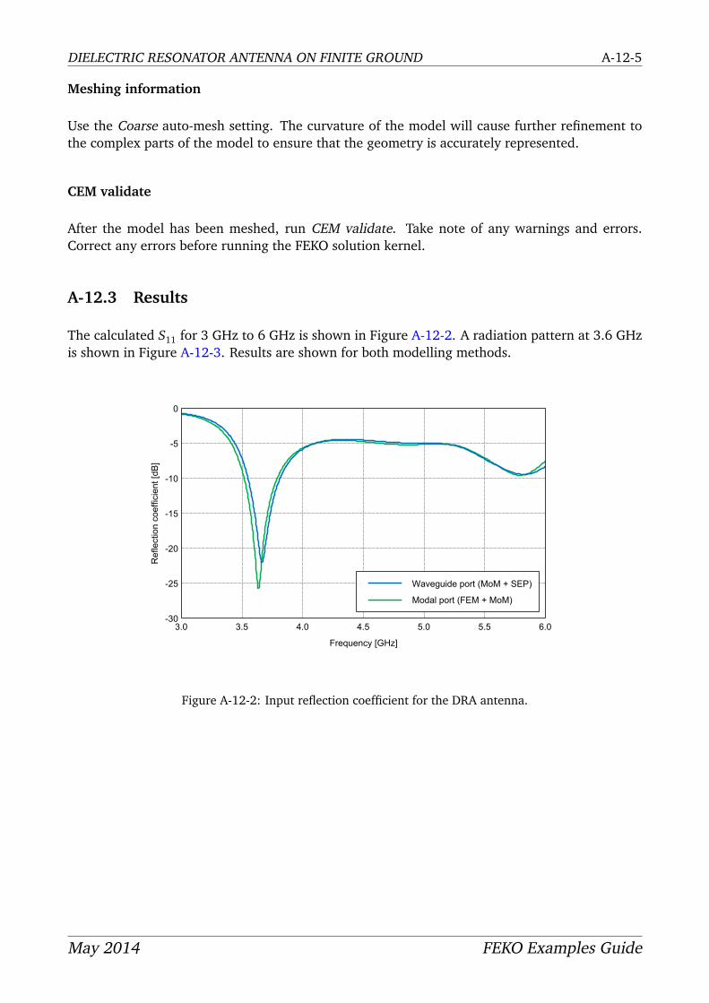
DIELECTRIC RESONATOR ANTENNA ON FINITE GROUND A-12-5
Meshing information
Use the Coarse auto-mesh setting. The curvature of the model will cause further refinement tothe complex parts of the model to ensure that the geometry is accurately represented.
CEM validate
After the model has been meshed, run CEM validate. Take note of any warnings and errors.Correct any errors before running the FEKO solution kernel.
A-12.3 Results
The calculated S11 for 3 GHz to 6 GHz is shown in Figure A-12-2. A radiation pattern at 3.6 GHzis shown in Figure A-12-3. Results are shown for both modelling methods.
-30
-25
-20
-15
-10
-5
0
3.0 3.5 4.0 4.5 5.0 5.5 6.0
Ref
lect
ion
coef
ficie
nt [d
B]
Frequency [GHz]
Waveguide port (MoM + SEP)
Modal port (FEM + MoM)
Figure A-12-2: Input reflection coefficient for the DRA antenna.
May 2014 FEKO Examples Guide

DIELECTRIC RESONATOR ANTENNA ON FINITE GROUND A-12-6
-20-15-10-505
030
60
90
120
150180
210
240
270
300
3300
Waveguide port (MoM + SEP)
Modal port (FEM + MoM)
Figure A-12-3: Vertical (XZ plane) gain (in dB) at 3.6 GHz.
May 2014 FEKO Examples Guide

A LENS ANTENNA WITH GEOMETRICAL OPTICS (GO) - RAY LAUNCHING A-13-1
A-13 Analysing a lens antenna using the geometrical optics(GO) - ray launching
Keywords: Geometrical optics, lens antenna, dielectric, radiation pattern, radiation patternpoint source
A-13.1 Creating the lens model
A dielectric lens with a spherical surface (S1) and elliptical surface (S2) is constructed. The lens isilluminated by a radiation pattern point source based on a precomputed cos4(x) radiation patternand the far field pattern is computed.
The lens structure is modelled using the geometrical optics (ray launching GO) method. Theresults are compared to the MoM/FEM result. The model is shown in Figure A-13-1.
Figure A-13-1: The 3D view of the dielectric GO lens model with a point excitation (symmetry planesshown).
Creating the model
The model is constructed in millimetres. It is assumed that the focal point of the lens is positionedat the global origin. A lens shape consisting of a spherical surface and an elliptical surface isassumed. The spherical surface is centred at the focal point.
The dielectric lens model has the following user defined parameters:
• freq = 30e9 (The operating frequency.)
• lambda_0 = c0/freq (Free space wavelength.)
• D = lambda_0*10 (Diameter of cylinder.)
• F = 1.5*D (Focal length.)
• epsr = 6 (The relative permittivity.)
• tand = 0.005 (Dielectric loss tangent.)
May 2014 FEKO Examples Guide

A LENS ANTENNA WITH GEOMETRICAL OPTICS (GO) - RAY LAUNCHING A-13-2
The following variables derived from the above variables are used in the model construction:
• alpha = arcsin(D/(2*F))(Included angle to edge of lens.)
• arclength = alpha*F (Arc length to edge of lens.)
• gL0 = arclength/10 (Mesh variable.)
• n = sqrt(epsr) (Refraction index.)
• T = (2 ∗ F − sqr t(4 ∗ F2− D2))/(2 ∗ (n− 1)) (Lens thickness.)
• v0= (F + T )/(n+ 1) (Ellipse offset distance.)
• u0= sqr t(n2− 1) ∗ v0 (Ellipse minor axis length.)
• w0= n ∗ v0 (Ellipse major axis length.)
A dielectric medium named Glass is defined and the relative permittivity and loss tangent are setto the variables epsr and tand, respectively.
To construct the lens, a sphere will be subtracted from an elliptical spheroid. The steps are asfollow:
• Create a sphere at the origin with a radius F.
• Create a spheroid (by choosing the Centre, radius U, radius V, radius N method whencreating a sphere). Its properties are:
– Centre: (0,0,v0)
– Radius (Ru): u0
– Radius (Rv): u0
– Radius (Rn): w0
• Subtract the sphere from the spheroid; the resulting geometry can be labelled Lens.
• By default a closed region will be a perfect electric conductor. The region type of the Lenspart is changed to be dielectric Glass.
Requesting calculations
To model the dielectric lens with the geometrical optics approximation we need to specify thesolution method for the Lens.S1 and Lens.S2 faces. From the Solution tab of the Face propertiesdialogue select the Geometrical optics (GO) - ray launching solution method. In general to checkwhich solution methods are being applied, the user can use the View by solution parameters tool.
The geometrical optics approximation has two user options that affect the solution:
• Maximum no. of ray interactions (default = three)
May 2014 FEKO Examples Guide
A LENS ANTENNA WITH GEOMETRICAL OPTICS (GO) - RAY LAUNCHING A-13-3
• Ray launching settings (default = Automatic)
The present implementation does not take into account the local curvature at the interactionpoint. This assumption / approximation could fail when using a large number of ray interactionsand where the local curvature of the geometry can’t be neglected. These settings can also bechanged on the Solver settings → High frequency dialog. Unselect the automatic setting forthe angular increment. Set the dielectric GO ray launching settings for theta and phi, to 1.5
respectively.
The analysis is requested at a single frequency of 30 GHz. The dielectric lens is illuminated by aradiation pattern point source. The radiation pattern is X polarized and positioned at the focalpoint. The E field pattern is described by Ex = (cosθ)4, where 0 ≤ θ≤ pi/2 is the polar anglemeasured from the Z axis. The pattern data is read from a *.ffe file with 91 samples and 180samples in the polar and azimuth angles, respectively.
Far field pattern cuts (0 ≤ theta ≤ 180 degree) are calculated in the X Y plane (phi = 0) andY Z plane (phi = 90). The angular increment is set to 0.25 to capture the fine angular detail.
Meshing requirements
Generally the mesh size is determined by the smallest wavelength of interest. However whenusing the Geometrical optics (GO) - ray launching approximation, the mesh size is determinedby the geometry (i.e. the mesh size is chosen to obtain a reasonable faceted representation ofthe geometry). The run time depends on the number of triangles and it is advisable to not overdiscretise the geometry. For this example the arc length of the spherical arc ‘S1’ is used as a basisto determine the mesh size.
It is also possible to use the standard auto-meshing, but then the settings on the Advanced tab ofthe mesh dialog will have to be used to ensure better geometrical approximation.
CEM validate
After the model has been meshed, run CEM validate. Take note of any warnings and errors.Correct any errors before running the FEKO solution kernel.
A-13.2 Results
The results (as shown in Figure A-13-2) show the original input gain pattern of the point source.This is used as a reference to see the effect that the glass lens and the solution method has onthe gain patterns. Both the FEM and GO solutions show good agreement with one another andshow the expected focussing of the electric fields in the main beam direction. The memory andruntime requirements of running the GO model are orders of magnitudes lower than that of thefull-wave FEM solution.
May 2014 FEKO Examples Guide

A LENS ANTENNA WITH GEOMETRICAL OPTICS (GO) - RAY LAUNCHING A-13-4
-50-40-30-20-10010200
30
60
90
120
150180
210
240
270
300
3300
Gain
Reference
GO
FEM
Figure A-13-2: The computed radiation pattern compared to the reference solution and a full FEM result.
May 2014 FEKO Examples Guide

WINDSCREEN ANTENNA ON AN AUTOMOBILE A-14-1
A-14 Windscreen antenna on an automobile
Keywords: windscreen, input impedance, antenna
In this example we consider the input impedance of a windscreen antenna. Windscreen antennasare antennas that are located in or on a windscreen. The windscreen can consist of one or morelayers and the different layers do not have to be meshed and thus simulation time is greatlyreduced when compared to conventional methods. Figure A-14-1 shows a 3D representation ofthe car and windscreen being simulated in this example.
Figure A-14-1: 3D view of an automobile and a windscreen antenna.
A-14.1 Creating the rear windscreen model
The model is created by importing geometry instead of using CADFEKO’s geometry tools. Therequired geometry files for the import are available as part of your FEKO installation and islocated in the ExampleGuide_models directory.
Creating the model
The steps for setting up the model are as follows:
• Import the Parasolid geometry for the car (car_geometry.x_b). Set the scale equal to 1.
• Rename the three parts to be more descriptive of the geometry. There should be a part forthe car_body, one for the antenna and one for the windscreen.
• Union the car and the antenna. This ensures that these structures will be connected duringmeshing. Note that the windscreen is not part of the union.
• Add a wire port to the wire that connects the antenna to the car’s chassis. See Figure A-14-1for an indication of where this port is located. Ensure that a vertex wire port is createdinstead of the default segment wire port.
May 2014 FEKO Examples Guide

WINDSCREEN ANTENNA ON AN AUTOMOBILE A-14-2
• Add a voltage source to the port that has been created.
• Define the following dielectric materials:
– glass: εr=7; tanδ=0.03
– pvb_foil: εr=3; tanδ=0.05
• Create a layered dielectric called windscreen_layers with the following properties:
– Layer 1: 2.1 mm thick glass
– Layer 2: 0.76 mm thick pvb_foil
– Layer 3: 2.1 mm thick glass
• Create a new windscreen definition (similar to how a dielectric is created) that uses thewindscreen_layers layer definition. Set the Offset L=2.1e-3+0.76e-3. This places areference plane (i.e. the geometry to which this definition will be applied) between thepvb_foil and the bottom glass layer.
• Select the single face of the windscreen and set its properties so that it is solved usingthe Windscreen solution method is. This is a windscreen reference element and should bedisplayed in a semi-transparent colour that corresponds to the colour of the windscreendefinition. Keep in mind that windscreen reference elements are not solved with the wind-screen solution method, but they are use as part of the solution and define the shape andposition of the windscreen.
• Set a local mesh refinement of 0.6 on the windscreen reference face. The only require-ment for the mesh size is that the geometry should be accurately represented. Curvilinearelements are supported for windscreen reference faces and thus only a little refinement isrequired.
• Select the wires of the antenna, see Figure A-14-2. Set their solution method to be Wind-screen. These are windscreen solution elements. The offset is set to zero, so that thesolution elements are defined on the reference plane defined above. These elements willbe solved with the Windscreen.
• Set the frequency to be continuous from 90 – 110 MHz.
Figure A-14-2: Select the wires of the antenna.
May 2014 FEKO Examples Guide

WINDSCREEN ANTENNA ON AN AUTOMOBILE A-14-3
Request calculations
We are interested in the input impedance of the antenna and thus no solution requests are re-quired. The input impedance is automatically calculated for voltage sources.
Meshing information
Use the Standard auto-mesh setting with wire segment radius equal to 150e-6. Due to thefine detail in the geometry of the car, some advanced mesh settings should be utilised to avoidmeshing electrically negligible details. On the Advanced tab of the meshing dialog, set:
• the Refinement factor to Coarse
• the Minimum element size to Medium
Note that a local mesh refinement was set on the windscreen reference face to ensure that themesh accurately represents the geometry of the face. Roughly 5 curvilinear elements is enoughto accurately represent the geometry of the windscreen.
CEM validate
After the model has been meshed, run CEM validate and ensure that no errors or warnings arereported. The Solve/Run→ View by solution parameters dialog can be used to see (and ensure)that the correct elements have been selected as reference and solution elements.
A-14.2 Results
Save and run the FEKO solver. Figure A-14-3 shows the computed input impedance as a functionof frequency from 90 – 110 MHz. It is recommended to use MLFMM for simulation at higherfrequencies (500 MHz or more).
May 2014 FEKO Examples Guide

WINDSCREEN ANTENNA ON AN AUTOMOBILE A-14-4
0
50
100
150
200
90 92 94 96 98 100 102 104 106 108 110
Impe
danc
e [O
hm]
Frequency [MHz]
Real Imaginary
Figure A-14-3: Real and imaginary part of the input impedance of the windscreen antenna.
May 2014 FEKO Examples Guide

DESIGN OF A MIMO ELLIPTICAL RING ANTENNA (CHARACTERISTIC MODES) A-15-1
A-15 Design of a MIMO elliptical ring antenna (characteristicmodes)
Keywords: characteristic modes, eigen value, MIMO, multiple-input multiple-output
A characteristic mode analysis is performed on a ring structure. This analysis is independent ofany excitations and provide insight into how a structure resonates at the calculated frequencies.Using this knowledge, one can strategically excite a structure so that only the desired modes areutilised. Figure A-15-1 shows the first four electric far field modes for the ring structure.
Figure A-15-1: The first four electric far field modes for the MIMO ring.
A-15.1 MIMO ring
Creating the model
The steps for setting up the model are as follows:
• Define the following variables:
– rInU = 21 (Inner radius of the ring in the U direction.)
– rOutU = 31 (Outer radius of the ring in the U direction.)
– rInV = rInU*0.8 (Inner radius of the ring in the V direction.)
– rOutV = rOutU*0.8 (Outer radius of the ring in the V direction.)
– freq = 2.4e9 (Operating frequency.)
• Set the model to millimetres.
• Create an elliptic arc centred at the origin with a radius of rOutU and rOutV in the u- andv-dimensions respectively. Set the start and end angles from 0 – 90.
• Create another elliptic arc centred at the origin with a radius of rInU and rInV in the u-and v-dimensions respectively. Set the start and end angles from 0 – 90.
• Select the two curves and create a surface by using the Loft tool. Name the quarter ringsector_1.
May 2014 FEKO Examples Guide

DESIGN OF A MIMO ELLIPTICAL RING ANTENNA (CHARACTERISTIC MODES) A-15-2
– Copy and mirror sector_1 around the UN plane.
– Copy and mirror both sectors around the VN plane.
– Union all four sectors to create a single ring structure.
• Set the simulation frequency to freq.
• Create four edge ports as indicated:
Figure A-15-2: Position of the four ports relative to a top view of the ring.
– port_North: The port edge should fall on the positive Y axis.
– port_West: The port edge should fall on the negative X axis.
– port_South: The port edge should fall on the negative Y axis.
– port_East: The port edge should fall on the positive X axis.
Take note that all of the ports point in the same counter-clockwise direction.
Symmetry in general does not apply to characteristic mode analyses, since there is no activeexcitation involved. However, geometric symmetry can be applied to both the X=0 and Y=0planes. This will result in a symmetrical mesh.
Configurations
Three configurations will be created. The first will be to request the characteristic mode analysis.The other two configurations will illustrate how one can use the insights obtained from a char-acteristic mode analysis to excite specific modes. Ensure that loads and sources are specified perconfiguration before continuing.
1. Request a characteristic mode configuration. Only the first five modes should be calculated.
May 2014 FEKO Examples Guide

DESIGN OF A MIMO ELLIPTICAL RING ANTENNA (CHARACTERISTIC MODES) A-15-3
• Request all currents.
• Request a full 3D far field with default sampling.
2. Request a standard configuration. The purpose of this configuration is to excite the firstcharacteristic mode.
• Add a voltage source to the Eastern port: (1 V, 0, 50 Ω)
• Add a voltage source to the Western port: (1 V, 180, 50 Ω)
• Request all currents.
• Request a full 3D far field with default sampling.
3. Request a standard configuration. The purpose of this configuration is to excite the fifthcharacteristic mode.
• Add a source to the Eastern port: (1 V, 0, 50 Ω)
• Add a source to the Western port: (1 V, 0, 50 Ω)
• Add a source to the Northern port: (1 V, 180, 50 Ω)
• Add a source to the Southern port: (1 V, 180, 50 Ω)
• Request all currents.
• Request a full 3D far field with default sampling.
Meshing information
Use the Fine auto-mesh setting. On the Advanced tab of the mesh dialog, set the refinementfactor to Fine. This is to ensure that the geometry is accurately represented.
CEM validate
After the model has been meshed, run CEM validate. Take note of any warnings and errors.Correct any errors before running the FEKO solution kernel.
A-15.2 Results
Characteristic modes are the basic building blocks for many electromagnetic results. When ex-citations and loads are added to a solution, we unknowingly calculate a weighted sum of thevarious characteristic modes. The following results will show that if the characteristic modes areproperly understood, then one can alter the behaviour of a structure without making any changesto the geometry.
Note that when comparing the characteristic modes to the reconstructed modes, all values needto be normalised.
May 2014 FEKO Examples Guide

DESIGN OF A MIMO ELLIPTICAL RING ANTENNA (CHARACTERISTIC MODES) A-15-4
Figure A-15-3: MIMO ring’s first characteristic current mode (left) vs. the reconstructed mode (right).
Mode 1 comparison
Figure A-15-3 shows how the first characteristic mode (left) can be recreated when sources areplaced in the appropriate locations.
Mode 5 comparison
Figure A-15-4 shows how the fifth characteristic mode (left) can be recreated when sources areplaced in the appropriate locations.
Figure A-15-4: MIMO ring’s fifth characteristic current mode (left) vs. the reconstructed mode (right).
Electric far fields
Figure A-15-5 shows how the manually electric fields compare to the characteristic field modesthat were calculated using the characteristic modes. Note that due to the lack of excitations whenusing characteristic modes, that the results are normalised in this comparison.
May 2014 FEKO Examples Guide

DESIGN OF A MIMO ELLIPTICAL RING ANTENNA (CHARACTERISTIC MODES) A-15-5
0.10.20.30.40.50.60.70.80.9
030
60
90
120
150180
210
240
270
300
3300
Normalised electric far field
Characteristic mode 1
Recreated mode 1
Characteristic mode 4
Recreated mode 4
Figure A-15-5: A polar plot comparing the MIMO ring’s characteristic electric field modes with the recre-ated fields.
May 2014 FEKO Examples Guide

PERIODIC BOUNDARY CONDITIONS FOR ARRAY ANALYSIS A-16-1
A-16 Periodic boundary conditions for array analysis
Keywords: periodic boundary condition, voltage source, far field
The periodic boundary condition solution method is used to calculate the far field pattern for asingle element in an infinite 2D array of pin fed patch elements as well as the approximated farfield pattern for a 10× 10 element array. The mutual coupling between elements is taken intoaccount as though the elements were in an infinite array. This means that for large arrays, theresults will be very accurate if edge effects can be neglected.
Figure A-16-1: A 3D view of a single element of the infinite patch array.
A-16.1 Pin fed patch: Broadside pattern by phase shift definition
Creating the model
The steps for setting up the model are as follows:
• Define the following variables:
– lambda = 0.1 (The spacing for periodic boundary condition.)
– freq = c0/lambda (Operating frequency of the patch)
– er = 2.55 (Relative dielectric constant of patch substrate)
– base_width = 0.5*lambda (Width of the patch substrate)
– base_length = 0.5*lambda (Length of the patch substrate)
– base_height = 0.02*lambda (Height of the patch substrate)
– patch_width = 0.3*lambda (Width of the patch antenna)
– patch_length = 0.3*lambda (Length of the patch antenna)
– pin_pos = patch_length/4 (Distance of feed pin from patch centre)
• Create a dielectric medium named substrate with relative permittivity of er and zerodielectric loss tangent.
• Create the substrate using the cuboid primitive with the base centre, width, depth, heightdefinition method. The side lengths are base_width and base_length and has a thick-ness of base_height.
May 2014 FEKO Examples Guide

PERIODIC BOUNDARY CONDITIONS FOR ARRAY ANALYSIS A-16-2
• Create the patch by creating a rectangle with the base centre, width, depth, height defini-tion method. The base centre should be located at (0,0,base_height). Set the width anddepth respectively to the defined variable patch_length and patch_width.
• Create the feed pin as a wire between the patch and the bottom of the substrate. Set theStart point to (-pin_pos,0,0) and the End point to (-pin_pos,0,base_height).
• Union all the elements and label the union antenna.
• Set the region of the cuboid to substrate.
• Set the faces representing the patch and the ground below the substrate to PEC.
• Add a segment wire port on the middle of the wire.
• Add a voltage source on the port. (1 V, 0, 50 Ω)
• Set the frequency to freq.
• Set the periodic boundary condition of the model to the end exactly on the edge of thesubstrate to expand in both the x- and y-dimensions.
• Manually specify the phase shift in both directions to be u1=0 and u2=0.
Requesting calculations
The solution requests are:
• Create a vertical (E plane) far field request. (-180≤θ≤180, with θ=1 and φ=0 incre-ments).
• Create another vertical (E plane) far field request. (-180≤θ≤180, with θ=1 and φ=0
increments). This time, request the calculation of a 10 × 10 array of elements (on theAdvanced tab).
Meshing information
Use the standard auto-mesh setting with wire segment radius equal to 0.0001.
CEM validate
After the model has been meshed, run CEM validate. Take note of any warnings and errors.Correct any errors before running the FEKO solution kernel.
May 2014 FEKO Examples Guide

PERIODIC BOUNDARY CONDITIONS FOR ARRAY ANALYSIS A-16-3
A-16.2 Pin fed patch: Broadside pattern by squint angle definition
Creating the model
Use the same geometry as for the first model. Meshing instructions are also the same. Changethe periodic boundary condition settings as follow:
• Determine the phase shift by setting the beam angle for Theta and Phi to 0.
Requesting calculations
Use the same far field calculations as for the first model.
CEM validate
After the model has been meshed, run CEM validate. Take note of any warnings and errors.Correct any errors before running the FEKO solution kernel.
A-16.3 Pin fed patch: Squint pattern by phase shift definition
Creating the model
Use the same geometry as for the first model. Meshing instructions are also the same. Changethe periodic boundary condition settings as follow:
• Manually specify the phase shift in both directions to be u1=–61.56 and u2=0.
Requesting calculations
Use the same far field calculations as for the first model.
CEM validate
After the model has been meshed, run CEM validate. Take note of any warnings and errors.Correct any errors before running the FEKO solution kernel.
A-16.4 Pin fed patch: Squint pattern by squint angle definition
Creating the model
Use the same geometry as for the first model. Meshing instructions are also the same. Changethe periodic boundary condition settings as follow:
• Determine the phase shift by setting the beam angle for Theta=20 and Phi=0.
May 2014 FEKO Examples Guide
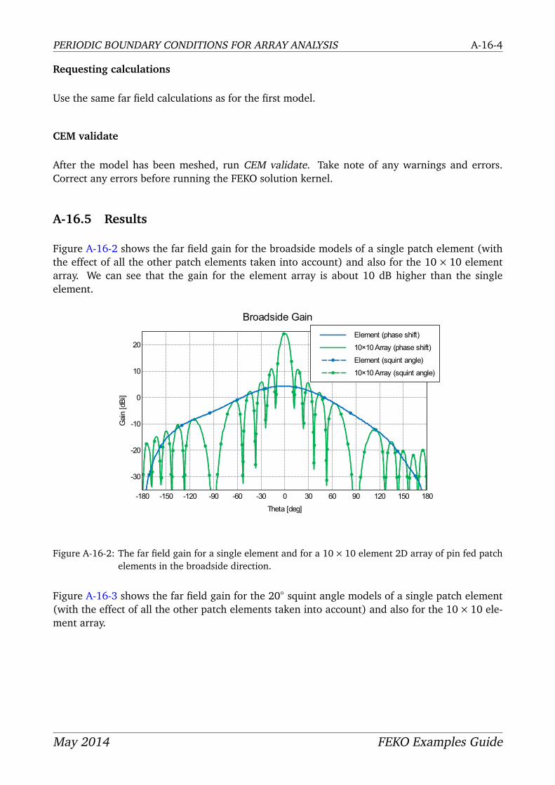
PERIODIC BOUNDARY CONDITIONS FOR ARRAY ANALYSIS A-16-4
Requesting calculations
Use the same far field calculations as for the first model.
CEM validate
After the model has been meshed, run CEM validate. Take note of any warnings and errors.Correct any errors before running the FEKO solution kernel.
A-16.5 Results
Figure A-16-2 shows the far field gain for the broadside models of a single patch element (withthe effect of all the other patch elements taken into account) and also for the 10× 10 elementarray. We can see that the gain for the element array is about 10 dB higher than the singleelement.
-30
-20
-10
0
10
20
-180 -150 -120 -90 -60 -30 0 30 60 90 120 150 180
Gai
n [d
Bi]
Theta [deg]
Broadside GainElement (phase shift)
10×10 Array (phase shift)
Element (squint angle)
10×10 Array (squint angle)
Figure A-16-2: The far field gain for a single element and for a 10× 10 element 2D array of pin fed patchelements in the broadside direction.
Figure A-16-3 shows the far field gain for the 20 squint angle models of a single patch element(with the effect of all the other patch elements taken into account) and also for the 10× 10 ele-ment array.
May 2014 FEKO Examples Guide

PERIODIC BOUNDARY CONDITIONS FOR ARRAY ANALYSIS A-16-5
-30
-20
-10
0
10
20
-180 -150 -120 -90 -60 -30 0 30 60 90 120 150 180
Gai
n [d
Bi]
Theta [deg]
Gain (20° Squint)
Element (phase shift)
10×10 Array (phase shift)
Element (squint angle)
10×10 Array (squint angle)
Figure A-16-3: The far field gain for a single element and for a 10× 10 element 2D array of pin fed patchelements in the 20 degree squint direction.
May 2014 FEKO Examples Guide

FINITE ARRAY WITH NON-LINEAR ELEMENT SPACING A-17-1
A-17 Finite array with non-linear element spacing
Keywords: finite array, DGFM
The finite array that is presented here consists of identical array elements that are arbitrarilyspaced. A pin-fed patch antenna serves as the base element for the array. The array is created byarbitrarily placing the base element (see figure A-17-2 for the array’s layout).
Arrays of this type are difficult to model and can result in high resource requirements. It willbe shown how the array can be constructed using the available finite array tools. When arraysare constructed in this way, the DGFM (domain Green’s function method) acceleration can beapplied to lower the resources that are needed.
Figure A-17-1 shows the full 3D far field pattern for the array.
Figure A-17-1: The 3D far field pattern for the array.
A-17.1 Pin-fed patch array
Creating the model
The steps for setting up the model are as follows:
• Define the following variables:
– freq = 2.4e9 (Operating frequency of the patch)
– lam0 = c0/freq*1000 (Free space wavelength in millimetres)
– epsr = 2.08 (Relative dielectric constant of patch substrate)
– patchLength = 41 (Length of the patch antenna)
– patchWidth = 35 (Width of the patch antenna)
– h = 3.5 (The height of the substrate)
– pinOffset = -11 (Distance of feed pin from patch centre)
– wireRadius = 0.1 (Radius of the feed pin wire)
• Set the model unit to millimetres.
May 2014 FEKO Examples Guide

FINITE ARRAY WITH NON-LINEAR ELEMENT SPACING A-17-2
• Create a rectangle centred at the origin with a width of patchWidth and a depth ofpatchLength.
• Create a line segment between (0,pinOffset,−h) and (0,pinOffset,0).
• Union the parts together.
• Create a dielectric medium with a permittivity of epsr and label it substrate.
• Create a planar multilayer substrate with a height of h. The medium should be substrate.Ensure that a ground plane is defined at the bottom of the dielectric layer.
• Add a port to the wire segment.
• Add a voltage source to the port with the default values.
• Set the frequency to freq.
λ 2λ
λ2λ
Figure A-17-2: The array layout that will be analysed.
The geometry above represents the base element, which is not included in the array calculationsby default. Create the array depicted in figure A-17-2 by performing the following steps:
• Create a planar array:
– Request four elements in both dimensions
– Space the elements lam0 apart
• Convert the planar array into a custom array. This makes it possible to delete, reposition orrotate individual elements of the array.
• Delete all elements corresponding to the third row and column. There should now be nineelements left.
Note that each element can also have a different orientation. Elements are rotated bymodifying the local workplane of the custom antenna array elements. No elements needto be rotated for this example, but the user in encouraged to rotate some of the elementsafter the simulation has completed to investigate the effect on the array pattern.
May 2014 FEKO Examples Guide

FINITE ARRAY WITH NON-LINEAR ELEMENT SPACING A-17-3
Meshing
Use Standard meshing to mesh the geometry. Set the segment radius to wireRadius.
Requests
Request a 3D far field that covers the top half space. A sampling increment of θ = 1.5 andφ = 1.5 is needed to obtain a reasonable resolution. Set the origin of the far field (Workplanetab) to 1.5*lam0 for both the X and the Y components. This does not change the far field pattern(this will affect the phase), but places the display of the far field on the 3D view in the middle ofthe patch array.
Note that a warning may be encountered when running the solution. This is because lossescannot be calculated in an infinitely large medium, as is required for the extraction of antennadirectivity information (gain is computed by default). This warning can be avoided by ensuringthat the far field gain be calculated instead of the directivity. This is set on the advanced tab ofthe far field request in the tree.
A-17.2 Results
Figure A-17-3 shows the comparison of two theta cuts of the array approximation with the resultsobtained using an equivalent full MoM model. The results compare favourably.
-40-30-20-10010
030
60
90
120
150180
210
240
270
300
3300
Gain
Phi=0o (Full)
Phi=0o (Array)
Phi=90o (Full)
Phi=90o (Array)
Figure A-17-3: The far field gain pattern for the array.
Apart from the relative ease of construction when using arrays, there is also a performance im-provement when using the array techniques. This will become more evident for arrays thatcontain a larger number of elements.
May 2014 FEKO Examples Guide

Chapter B
Antenna placement

ANTENNA COUPLING ON AN ELECTRICALLY LARGE OBJECT B-1-1
B-1 Antenna coupling on an electrically large object
Keywords: electrically large, MLFMM, CFIE, coupling, antenna placement, S-parameters
This example consists of a Rooivalk helicopter mock-up with three monopole antennas locatednear the front, middle and rear of the model respectively. S-parameters (coupling) are computedbetween the three antennas over a frequency range.
Figure B-1-1: 3D view of the helicopter.
NOTE: Due to calculations over a frequency range as well as the electrical size of the problem,several hours of computation time is required.
B-1.1 Helicopter
This example consists of complicated geometry and the model for this geometry is provided withthe FEKO installation. The important features of this model are briefly presented.
• The model is solved with the MLFMM - this is set under Solver settings.
• The Combined Field Integral Equation (CFIE) is used. This is set on the face properties. Allof normals of the geometry faces must point outward.
Requesting calculations
The solution requests are:
• The S-parameters for this model must be calculated. All three ports should be included andall must be active with a reference impedance of 50 Ω.
CEM validate
After the model has been meshed, run CEM validate. Correct any warnings and errors beforerunning the FEKO solution kernel.
Note that during the FEKO solver run, the following warning may be displayed: Inhomogeneoussegmentation for triangles. This warning is due to the occurrence of both very large and smalltriangles in the rotor of the helicopter. This warning may be ignored for this example.
May 2014 FEKO Examples Guide

ANTENNA COUPLING ON AN ELECTRICALLY LARGE OBJECT B-1-2
B-1.2 Results
This example requires considerable time to solve (as shown in the extract below from the text*.out file). These resource requirements (both time and memory) for the MLFMM solutionare considerably smaller than for the full MoM solution. The resource requirements are furtherreduced in this example by the application of the CFIE formulation to the closed PEC structure ofthe helicopter. In this case, the use of the CFIE requires 30% less memory resources, and halvesthe simulation time required when compared with the default EFIE solution.
SUMMARY OF REQUIRED TIMES IN SECONDS
CPU-time runtimeReading and constructing the geometry 0.880 0.907Checking the geometry 0.450 0.451Initialisation of the Green’s function 0.000 0.000Calcul. of coupling for PO/Fock 0.000 0.000Ray-launching phase of GO 0.000 0.000Calcul. of the FMM transfer function 12.800 12.812Fourier transform of FMM basis funct. 61.980 62.014Calcul. of matrix elements 5175.980 5178.524Calcul. of right-hand side vector 0.020 0.018Preconditioning system of linear eqns. 26.720 26.751Solution of the system of linear eqns. 578.530 578.999Eigensolution for characteristic modes 0.000 0.000Determination of surface currents 0.000 0.000Calcul. of impedances/powers/losses 0.000 0.004Calcul. of averaged SAR values 0.000 0.000Calcul. of power ideal receiving ant. 0.000 0.000Calcul. of cable coupling 0.000 0.000Calcul. of error estimates 0.000 0.000Calcul. of electric near field 0.000 0.000Calcul. of magnetic near field 0.000 0.000Calcul. of far field 0.000 0.000
other 6.560 7.106----------- -----------
total times: 5863.920 5867.586(total times in hours: 1.629 1.630)
Peak memory usage during the whole solution: 315.522 MByte
The S-parameters representing the coupling between the antennas mounted on the helicopterand the reflection coefficients of the antennas are shown in Figure B-1-2 as a function of fre-quency.
May 2014 FEKO Examples Guide

ANTENNA COUPLING ON AN ELECTRICALLY LARGE OBJECT B-1-3
-60
-50
-40
-30
-20
-10
0
180 182 184 186 188 190 192 194 196 198 200
S-pa
ram
eter
s [d
B]
Frequency [MHz]
S-parameter = S1,1S-parameter = S2,1S-parameter = S3,1
-26
-24
-22
-20
-18
-16
-14
-12
-10
-8
-6
180 182 184 186 188 190 192 194 196 198 200
S-pa
ram
eter
s [d
B]
Frequency [MHz]
S-parameter = S1,1S-parameter = S2,2S-parameter = S3,3
Figure B-1-2: The input reflection coefficients and coupling between the antennas when mounted on theelectrically large helicopter.
May 2014 FEKO Examples Guide

ANTENNA COUPLING USING AN IDEAL RECEIVING ANTENNA B-2-1
B-2 Antenna coupling using an ideal receiving antenna
Keywords: coupling, ideal receiving antenna, far field data file, ffe file, helix antenna Yagi-Udaantenna, electrically large
This example involves the calculation of the coupling between a helix antenna and a Yagi-Udaantenna located in front of an electrically large metal plate, as shown in Figure B-2-1.
This is an electrically large problem, and two approaches are used to accelerate the solution sig-nificantly. The plate is efficiently modelled as an UTD plate and the helix antenna is modelledas an ideal receiving antenna. The receiving antenna can be modelled using a far field radiationpattern, far field spherical modes or a near field aperture. The ideal receiving antenna formula-tion can be used only when the required far field, spherical mode or near field aperture data isavailable (or can be calculated in a separate simulation) for an antenna. In addition, the antennamust be located an acceptable distance from all other physical structures that may influence thecurrents on the antenna.
This example will illustrate the use of all three receiving antenna techniques in a single model.The simulation time, received power and coupling between the antennas modelled using thethree receiving antenna formulations will be compared to the full solution. Note that usuallyonly one of these receiving antennas would be required in a model.
Figure B-2-1: Geometry of Antenna_Coupling showing full helix model.
Three models are provided for this example:
Antenna_Coupling_Helix_Antenna.cfx Model of the helix antenna used to pre-calculatethe far field pattern, spherical modes and near field aperture that will be used in the idealreceiving antennas.
Antenna_Coupling_Receiving_Antenna.cfx The model used to calculate the coupling be-tween the Yagi-Uda and helix antennas using the ideal receiving antenna techniques.
Antenna_Coupling_Full.cfx The model used to calculate reference result using the fullmodels for both antennas.
B-2.1 The helix antenna in free space
Creating the model
The steps for setting up the model are as follows:
May 2014 FEKO Examples Guide

ANTENNA COUPLING USING AN IDEAL RECEIVING ANTENNA B-2-2
• Define variables:
– freq = 1.654e9 (The design frequency of the helix.)
– lambda = c0/freq (The wavelength in free space.)
– n = 10 (The number of turns for the helix.)
– helix_alpha = 13 (The pitch angle of the helix.)
– helix_radius = lambda*cos(helix_alpha*pi/180)/pi/2 (The radius of thehelix.)
– plate_radius = 0.75*lambda (The radius of the ground plate.)
– wire_radius = 0.65e-3 (The radius of the helix wire segments.)
• An ellipse primitive is used to create a circular plate, centred around (0,0,0) with a radiusof plate_radius. This is used to model the finite ground plane of the helix.
• The helix antenna is created using a Helix primitive with:
– Definition method of Base centre, radius, pitch angle, turns.
– Origin at (0,0,0).
– Radius of helix_radius.
– Pitch angle of helix_alpha.
– Number of turns is n.
• The Helix and Ellipse are unioned to indicate connectivity.
• A wire port is added on the segment at the start of the Helix.
• A voltage excitation is applied to the port.
• Set the frequency to freq.
Meshing information
Use the standard auto-mesh setting with wire segment radius equal to wire_radius.
Requesting calculations
A full 3D far field is requested. The far field pattern receiving antenna requires a far field patternfile to be exported. On the Advanced tab, choose to export the field to an ASCII file. The far fieldpattern will be stored in a file with the *.ffe extension.
The spherical modes required for the spherical mode receiving antenna can be calculated aspart of the same far field request. On the Advanced tab, choose to calculate spherical modecoefficients and also to export the coefficients to an ASCII file. The spherical mode expansioncoefficients will be stored in a file with the *.sph extension.
The near field aperture receiving antenna requires near field points around the antenna to becalculated and stored. The near field aperture can be any shape and the aperture can also be
May 2014 FEKO Examples Guide

ANTENNA COUPLING USING AN IDEAL RECEIVING ANTENNA B-2-3
constructed from multiple near field request surfaces. It is important that the near field surfacespans the entire radiating area of the antenna. For the helix antenna the surface needs to be allaround the antenna and thus using spherical near field surface would work well. Create a nearfield request with the following settings:
• Use the spherical coordinate system.
• On the Advanced tab, choose to export the fields to ASCII file.
• Request the following ranges:
Axis Start End Increment
r 0.45 0.45 0θ 0 180 5φ 0 360 5
The files generated by this simulation will be used in the following model of this example.
B-2.2 Using receiving antenna techniqes to model the helix antenna
In the Antenna_Coupling_Receiving_Antenna.cfx model, the Yagi-Uda antenna and thelarge conducting sheet are added. The receiving antenna is correctly positioned and rotatedrelative to these by specifying a local coordinate system.
Creating the model
The steps for setting up the model are as follows:
• Define variables.
– freq = 1.654e9 (Design frequency of the helix.)
– lambda = c0/freq (The wavelength in free space.)
– yagi_ld = lambda*0.442 (The length of director element.)
– yagi_li = lambda*0.451 (The length of active element.)
– yagi_lr = lambda*0.477 (The length of reflector element.)
– yagi_d = 0.25*lambda (Spacing between yagi elements.)
– yagi_rho = lambda*0.0025 (The radius of yagi elements.)
• Define named points.
– helix_centre = (-1.5/2 , 3/4 , 1.5) as the helix antenna location
– yagi_centre = (-1.5/2 , -3/4 , 1.5) as the Yagi-Uda antenna location
• The Yagi-Uda antenna is created using line primitives. Create a line with start point (0,0,-yagi_li/2) and end point as (0,0,yagi_li/2). Set the label to yagi_active.
May 2014 FEKO Examples Guide

ANTENNA COUPLING USING AN IDEAL RECEIVING ANTENNA B-2-4
• Create a line with start point (0, -yagi_d, -yagi_ld/2) and end point (0, -yagi_d,yagi_ld/2). Set the label to yagi_director.
• Create a line with the start point (0, yagi_d, -yagi_lr/2) and the end point (0, yagi_d,yagi_lr/2). Set the label to yagi_reflector.
• Create a copy of yagi_director. Translate form (0,0,0) to (0,-yagi_d,0).
• Create a copy of yagi_director. Translate form (0,0,0) to (0,-2*yagi_d,0).
• Union the wires and modify the label to yagi_antenna.
• A wire port is added on the vertex at the centre of the active element of the yagi antenna.
• A voltage excitation is applied to the port.
• Set the simulation frequency to freq.
• Rotate yagi_antenna with -(90+15). Note that an expression may be added to the field,not just a value.
• Translate yagi_antenna from (0,0,0) to (yagi_centre, yagi_centre, yagi_centre).
• The rectangle primitive is used to create the plate:
– Set the local workplane to the global Y Z plane (Ctrl+Shift and click on the Global YZworkplane.
– Use the Base corner, width, depth with the corner at (-3,0,0).
– Set width = 6 and depth = 3.
Set the label to metal_plate.
• The properties of the rectangle face in the details tree are set so that the UTD method willbe applied to the face.
Meshing information
Use the standard auto-mesh setting with wire segment radius equal to yagi_rho.
Requesting calculations
• An ideal far field receiving antenna request is created
– The number of Theta and Phi points is 37 and 73 respectively. (If changes have beenmade to the provided models, care should be taken to ensure that the number of field-points specified for the receiving antenna is consistent with the values stored in the*.ffe file.)
– The pattern file is chosen as the *.ffe file generated using the free-space helix model.
– The origin of the workplane is set to the helix_center named point. The U axis direc-tion is (1,0,1) to define the orientation of the helix that the pattern represents.
May 2014 FEKO Examples Guide

ANTENNA COUPLING USING AN IDEAL RECEIVING ANTENNA B-2-5
• An ideal spherical mode receiving antenna request is created
– The spherical mode expansion file is chosen as the *.sph file generated using thefree-space helix model.
– The origin of the workplane is set to the helix_center named point. The U axis direc-tion is (1,0,1) to define the orientation of the helix that the pattern represents.
– Be sure to use the far field approximation for the internal approximation of the spher-ical modes receiving antenna. In cases where the request is very close to geometry,using spherical modes for the internal approximation may be inaccurate.
• An ideal near field receiving antenna request is created
– The near fields files is chosen as the *.efe and *.hfe files for electric and magneticnear fields respectively. These files were generated using the free-space helix model.
– Select the spherical coordinate system.
– The radius should be set to 0.45.
– The number of Theta and Phi points is 37 and 73 respectively. (If changes have beenmade to the provided models, care should be taken to ensure that the number of field-points specified for the receiving antenna is consistent with the values stored in the*.efe and *.hfe files.)
– The origin of the workplane is set to the helix_center named point. The U axis direc-tion is (1,0,1) to define the orientation of the helix that the pattern represents.
The Yagi-Uda antenna is oriented so that its first side-lobe is aimed directly at the helix. Theradiated power is configured as 100 W by selecting the Total source power (no mismatch) optionon the power settings dialog.
CEM validate
After the model has been meshed, run CEM validate. Take note of any warnings and errors.Correct any errors before running the FEKO solution kernel.
B-2.3 The full model
The ideal receiving antenna calculates the coupling assuming a matched load. To make the resultsdirectly comparable, the helix antenna in the full model is loaded with the complex conjugate ofits input impedance. The power loss in the applied load represents the total power received bythe antenna. This can be found in the *.out file.
B-2.4 Results
As coupling parameters cannot be computed directly when using the ideal receiving antenna,the coupling information must be derived from received power information. In POSTFEKO the
May 2014 FEKO Examples Guide

ANTENNA COUPLING USING AN IDEAL RECEIVING ANTENNA B-2-6
received power may be plotted on a graph or found in the text-based output of the *.out file.On the same graph, the power lost in the matching load from the full model may be plotted.
As we have chosen the radiated power to be exactly 100 W for all cases, the coupling can becalculated from:
Coupling(dB) = 10 ∗ log10
Received power
100
The comparative results are shown in Table B-2-1.
Received power (mW) Coupling (dB) Runtime (s)
Full model 3.2296 -44.91 140.370Receiving antenna (far field pattern) 3.0477 -45.16 <13Receiving antenna (spherical modes) 3.0735 -45.12 <13Receiving antenna (near field) 2.9418 -45.31 <13
Table B-2-1: Coupling results with 100 W transmitted power.
The power-loss computed in the full model is shown in this extract from the output file namedAntenna_Coupling_Full.out
POWER LOSS METAL (in Watt)
Losses due to impedances at vertices/connection pointsbasis fu. no. power loss1193 3.2296E-03 W
Total loss in the vertices: 3.2296E-03 W
Loss metal (total): 3.2296E-03 W W
Both the power lost in the conjugate load (from the full model) and the power received by theideal receiving antennas can be plotted in POSTFEKO.
Receiving antenna (far field pattern) with name: FarfieldReceivingAntenna1
RECEIVED POWER FOR IDEAL RECEIVING ANTENNA (FAR FIELD PATTERN)
Received power (ideal match assumed): 3.0477E-03 W
Relative phase of received signal: 4.6809E+00 deg.
Receiving antenna (spherical modes) with name: RXAntenna1
RECEIVED POWER FOR IDEAL RECEIVING ANTENNA (FAR FIELD PATTERN)
Received power (ideal match assumed): 3.0735E-03 W
Relative phase of received signal: 3.4302E+00 deg.
Receiving antenna (near field aperture) with name: NearfieldReceivingAntenna1
RECEIVED POWER FOR RECEIVING ANTENNA (NEAR FIELD APERTURE)
Received power: 2.9418E-03 W
The phase is relative to the global FEKO phase reference.
The ideal receiving antenna solutions requires considerably less resources than the full model. Ifthe receiving antenna is moved further away from the transmitting antenna and geometry, thenthe difference in the results will be smaller.
May 2014 FEKO Examples Guide

USING A POINT SOURCE AND IDEAL RECEIVING ANTENNA B-3-1
B-3 Antenna coupling using a point source and ideal receivingantenna
Keywords: coupling, S-parameters, radiation pattern point source, ideal receiving antenna
This example demonstrates the computation of coupling between two horn antennas using aradiation pattern point source approximation and an ideal far field pattern receiving antenna.The far field radiation point source can also be replaced by a spherical mode source. The receivingantenna can be modelled as a spherical mode source or a near field aperture source instead ofthe far field pattern receiving antenna. The best options for the source and the receiving antennadepends on the problem at hand. It is left to the reader to experiment with the different sourceand receiving antenna modelling techniques.
The model geometry consists of two horn antennas pointing towards one another, separated bya distance of 60 wavelengths. Exactly half way between the antennas is a metallic plate that iseffectively blocking the line–of–sight coupling between the antennas.
Figure B-3-1: The full 3D model representation of the problem considered in this example.
This example consists of 3 models.
Pyramidal_Horn.cfx A model of a horn antenna in free space used to precompute the far fieldradiation pattern to be used in the point source radiation pattern and ideal receiving an-tenna parts of the ensuing models.
Point_Source_Coupling.cfx A model that uses the far field radiation pattern of the horn antennato efficiently extract the coupling between two horns as shown in Figure B-3-1.
Full_Model.cfx The reference model used to compute the coupling between two horn antennaslocated as shown in Figure B-3-1 directly without using a precomputed far field pattern.
B-3.1 The horn antenna in free space
In the Pyramidal_Horn.cfx model shown in Figure B-3-2 the 3D radiation pattern of a horn at1.645 GHz is computed and saved to an *.ffe file. The horn is excited using a waveguide port.
The horn is placed with its excitation on the Y Z plane. To account for the phase centre offset,the far field is calculated with the offset axis origin at X= -21.6 cm. Two planes of symmetry areused in the model in the Y = 0 and Z = 0 planes.
May 2014 FEKO Examples Guide

USING A POINT SOURCE AND IDEAL RECEIVING ANTENNA B-3-2
The calculation of the phase centre that is required for accurate placement of the radiation pat-tern of the horn is beyond the scope of this example, but is discussed in Example 35 of theScriptExamples.pdf guide. A phase centre calculation script is also available on the FEKO websitethat allows the phase centre to be calculated in POSTFEKO. Technically, the phase offset needsto be calculated for each frequency. The far field pattern should also be calculated for eachfrequency. Due to the narrow bandwidth of the calculation, this step is omitted in this example.
B-3.2 Using the computed horn radiation pattern in a coupling calculation
In Point_Source_Coupling.cfx, the two horn antennas are substituted with a correctly ori-ented and positioned ideal receiving antenna and a radiation pattern point source.
The coupling can be computed based on the power that is received (in W) by the receivingantenna and comparing it to the power that was transmitted. By setting the transmitting antennapower to 1 W (on the power settings tab), only the received power needs to be recorded. Thecoupling is then related to the received power by:
Coupling(dB) = 10 ∗ log10
Received power
Transmitted power
B-3.3 The reference model
In Full_Model.cfx, both horns and the plate are included. Symmetry is used in the Y = 0 andZ = 0 planes.
The coupling between the antennas is computed directly by requesting S-parameters.
CEM validate
After the model has been meshed, run CEM validate. Take note of any warnings and errors.Correct any errors before running the FEKO solution kernel.
B-3.4 Results
The received power at the ideal receiving antenna is extracted from POSTFEKO. Figure B-3-3shows the fully calculated model compared to the point source approximation. It can be seenthat the results match reasonably well, where the differences can be attributed to the pointsource approximation.
Figure B-3-2: The 3D model of the horn that is used to generate the *.ffe file.
May 2014 FEKO Examples Guide

USING A POINT SOURCE AND IDEAL RECEIVING ANTENNA B-3-3
-27.5
-27.0
-26.5
-26.0
-25.5
-25.0
-24.5
1.60 1.61 1.62 1.63 1.64 1.65 1.66 1.67 1.68 1.69 1.70
Coup
ling
[dB]
Frequency [GHz]
Coupling between antennas
Full model
Point source approx.
Figure B-3-3: The comparative results for the full model simulation and the simulation using pre-calculated radiation pattern representations of the horn antennas in the model.
May 2014 FEKO Examples Guide

Chapter C
Radar cross section (RCS)

RCS OF A THIN DIELECTRIC SHEET C-1-1
C-1 RCS of a thin dielectric sheet
Keywords: RCS, thin dielectric sheet (TDS), plane wave
The electrically thin dielectric plate, modelled with the thin dielectric sheet approximation, isilluminated by an incident plane wave such that the bistatic radar cross section may be calculatedat 100 MHz.
Figure C-1-1: A 3D representation of a thin dielectric sheet with a plane wave excitation (excitation andsymmetry planes shown).
C-1.1 Dielectric sheet
Creating the model
The steps for setting up the model are as follows:
• Define the following variables:
– freq = 100e6 (Operating frequency.)
– d = 0.004 (Plate thickness.)
– a = 2 (Width of plate.)
– b = 1 (Depth of plate.)
– epsr = 7 (Relative permittivity.)
– tand = 0.03 (Loss tangent.)
– thetai = 20 (Zenith angle of incidence.)
– phii = 50 (Azimuth angle of incidence.)
– etai = 60 (Polarisation angle of incident wave.)
• Create a dielectric called substrate with relative permittivity equal to epsr and dielectricloss tangent set to the value of tand.
• Create a layered dielectric with a single layer named thin_dielsheet. Select substrateas the dielectric material for the layer and set the thickness equal to variable d.
May 2014 FEKO Examples Guide

RCS OF A THIN DIELECTRIC SHEET C-1-2
• Create a rectangular plate in the X Y plane centred around the origin. The width (X axis)is the value of a and depth is b.
• Set the face medium property of the plate to thin_dielsheet.
• Add a single incident plane wave excitation from the direction θ=thetai and φ=phii.Set the polarisation angle to etai.
• Set the frequency to freq.
Requesting calculations
The geometry of the problem is symmetric around the X=0 and Y=0 planes, but the excitationhas no symmetry. Two planes of geometric symmetry are therefore specified in the model settings.
The solution requests are:
• Create a vertical far field request. (-180≤θ≤180, with φ=0)
Meshing information
• Use the standard auto-mesh setting.
CEM validate
After the model has been meshed, run CEM validate. Take note of any warnings and errors.Correct any errors before running the FEKO solution kernel.
C-1.2 Results
The bistatic RCS of the dielectric sheet at 100 MHz as a function of the angle θ , in the planeφ = 0 is shown in Figure C-1-2.
May 2014 FEKO Examples Guide

RCS OF A THIN DIELECTRIC SHEET C-1-3
-55
-50
-45
-40
-35
-30
-25
-180 -150 -120 -90 -60 -30 0 30 60 90 120 150 180
RCS
[dBm
2]
Theta [deg]
Radar cross section
Figure C-1-2: Bistatic RCS of a thin dielectric sheet.
May 2014 FEKO Examples Guide

RCS AND NEAR FIELD OF A DIELECTRIC SPHERE C-2-1
C-2 RCS and near field of a dielectric sphere
Keywords: dielectric, plane wave, sphere, bistatic RCS, monostatic RCS
A lossless dielectric sphere with radius of 1 m and relative permittivity equal to 36 is excited bymeans of an incident plane wave. The wavelength of the incident field is 20 m in free space(3.33 m in the dielectric). The near field inside and outside the sphere as well as the RCS of thesphere are calculated and compared to theoretical results.
The calculation is done using the surface equivalence principle.
Figure C-2-1: A 3D view of the dielectric sphere and plane wave excitation. The CADFEKO preview of thefar field request and the symmetry planes are also shown on the image.
C-2.1 Dielectric sphere
Creating the model
The steps for setting up the model are as follows:
• Define the following variables:
– lambda = 20 (Free space wavelength.)
– freq = c0/lambda (Operating frequency.)
– radius = 1 (Sphere radius.)
– epsilon = 36 (Relative permittivity.)
• Create a new dielectric called diel and set its relative permittivity equal to epsilon.
• Create a sphere with at the origin and set its radius to the value of radius.
• Set the region properties of the sphere to be of medium diel.
• Add a plane wave excitation with θ=180 and φ=0.
• Set the frequency equal to variable freq (≈ 15 MHz).
May 2014 FEKO Examples Guide

RCS AND NEAR FIELD OF A DIELECTRIC SPHERE C-2-2
Requesting calculations
The geometry in this problem is symmetric around all 3 principal planes, but the excitation isnot. As the electric fields of the incident plane wave are purely X directed for the chosen incidentangle, electric symmetry may be used in the X=0 plane, magnetic symmetry may be used in theY=0 plane, but only geometric symmetry may be used in the Z=0 plane.
The solution requests are:
• Create a vertical far field request. (0≤θ≤180 and φ=0)
• Create a near field request along the Z axis. Set the Start position for the near field to(0,0,-2*radius) and the End position to (0,0,2*radius). Request 80 field points in the Zdirection.
Meshing information
Use the custom mesh option with the following settings:
• Triangle edge length: 0.2.
• Wire segment length: Not applicable.
• Tetrahedral edge length: Not applicable.
• Wire segment radius: Not applicable.
Since the wavelength at the simulation frequency is large compared to the size of the model, weneed to mesh the model such that it accurately represents a sphere. A triangle edge length of0.2 is fine enough to accurately represent the sphere.
CEM validate
After the model has been meshed, run CEM validate. Take note of any warnings and errors.Correct any errors before running the FEKO solution kernel.
C-2.2 Results
Figures C-2-2 and C-2-3 compare the near field along the Z axis and the radar cross section as afunction of the angle to exact mathematical results.
RCS calculations are displayed on a far field graph. The Y axis of the RCS graph has beenchanged to a logarithmic scale for improved visualisation.
May 2014 FEKO Examples Guide

RCS AND NEAR FIELD OF A DIELECTRIC SPHERE C-2-3
-20
-15
-10
-5
0
-2.0 -1.5 -1.0 -0.5 0.0 0.5 1.0 1.5 2.0
E-Fi
eld
[dBV
/m]
Z position [m]
E-Field
Exact
FEKO
Figure C-2-2: Near field along the Z axis.
-60
-50
-40
-30
-20
-10
0
0 30 60 90 120 150 180
RCS
[dBm
2]
Theta [deg]
RCS
Exact
FEKO
Figure C-2-3: Bistatic radar cross section of the dielectric sphere.
May 2014 FEKO Examples Guide

SCATTERING WIDTH OF AN INFINITE CYLINDER C-3-1
C-3 Scattering width of an infinite cylinder
Keywords: periodic boundary condition, plane wave, MoM
Using a 1-dimensional periodic boundary condition, the scattering of an infinite cylinder is ef-ficiently computed (as defined below). The results are compared with a literature reference(C. A. Balanis, Advanced Engineering Electromagnetics, Wiley, 1989, pp. 607.)
SW =1
λlimρ→∞[2πρ
| Esz |
2
| E iz |
2 ]
Figure C-3-1: A 3D view of the unit-cell of the infinite cylinder with the 1-D periodic boundary conditionshown.
C-3.1 Infinite cylinder
Creating the model
The model consists of a cylindrical section of variable radius and height of half a wavelength atthe excitation frequency. The cylinder is realised by creating a cylinder primitive and deleting theupper and lower faces of the cylinder.
Requesting calculations
For this example, the scattering width of the cylinder for an incident plane wave normal to thecylinder will be considered. A plane wave excitation for θ=90 and φ=180 is used.
The 1D periodic boundary condition is defined along the axis of the cylinder so that the unit-celltouches the edges of the periodic region.
A near field request is used to determine the direction-dependent scattered field, from which thescattering width is derived:
• Request a cylindrical coordinate system near field
• Set the radius as: ρ=500*lambda
May 2014 FEKO Examples Guide

SCATTERING WIDTH OF AN INFINITE CYLINDER C-3-2
• Specify φ=0.5 angular resolution
• It is important to only calculate the scattered part of the near field. This removes the effectof the plane wave on the calculated field and ensures that only the scattered fields areconsidered.
The calculation is performed at a frequency of 299.8 MHz (wavelength of 1 m).
Meshing information
Use the fine auto-mesh setting. Also try modifying the parameters on the advanced tab to obtaina mesh that better represents the geometry as a cylinder.
It is also possible and recommended to simulate the same model using higher order curvilinearelements. Ensure that higher order basis functions are enabled on the Sover settings dialog. Thecurvilinear elements are a better approximation of the geometry and standard meshing results inan accurate geometrical representation.
CEM validate
After the model has been meshed, run CEM validate. Take note of any warnings and errors.Correct error before running the FEKO solution kernel.
C-3.2 Results
Figure C-3-2 shows the computed scattering width as a function of the bistatic observation angle(φ) for two different cylinder radii. The results agree well with the literature reference.
The scattering width was obtained by using the equation at the top of the example with thevalues provided to simplify to
SW = 2π500 | E | 2.
To use the equation, ensure the magnitude of the electric field is displayed and activate the Enablemaths. Enter the following equation in POSTFEKO:
2*pi*500*ABS(self)^2
May 2014 FEKO Examples Guide

SCATTERING WIDTH OF AN INFINITE CYLINDER C-3-3
Figure C-3-2: The scattering width of an infinite cylinder with two different radii modelled.
May 2014 FEKO Examples Guide

PERIODIC BOUNDARY CONDITIONS FOR FSS CHARACTERISATION C-4-1
C-4 Periodic boundary conditions for FSS characterisation
Keywords: periodic boundary condition, plane wave, frequency selective surface, near field,optimisation
A Jerusalem cross FSS (frequency selective surface) structure modelled using infinite periodicboundary conditions is excited with an incident plane wave (as shown in Figure C-4-1). Thefrequency dependent transmission and reflection coefficients of the surface are computed andconsidered. These results may be compared to those reported in the literature (Ivica Stevanovic,Pedro Crespo-Valero, Katarina Blagovic, Frederic Bongard and Juan R. Mosig, Integral-EquationAnalysis of 3-D Metallic Objects Arranged in 2-D Lattices Using the Ewald Transformation, IEEETrans. Microwave Theory and Techniques, vol. 54, no. 10, October 2006, pp. 3688–3697).
Note that the model supplied with this example includes an optimisation set up to determine thebest set of geometrical parameters to maximise reflection and minimise transmission at 8 GHz.To perform the optimisation the frequency request should be set to a single frequency equal to8 GHz.
Figure C-4-1: A 3D view of the FSS structure. The Jerusalem cross unit-cell structure is shown with theplane wave excitation and periodic boundary condition.
C-4.1 Frequency selective surface
Creating the model
The steps for setting up the model are as follows:
• Define the following variables:
– d = 15.2 (The spacing for periodic boundary condition.)
– armLength = 13.3 (The length of the arm of the cross.)
– armWidth = 1.9 (The width of the arm of the cross.)
– stubLength = 5.7 (Length of stub at the end of the cross.)
– stubWidth = armWidth (Width of stub at the end of the cross.)
– fmin = 2e9 (The minimum frequency.)
May 2014 FEKO Examples Guide

PERIODIC BOUNDARY CONDITIONS FOR FSS CHARACTERISATION C-4-2
– fmax = 12e9 (The maximum frequency.)
• Set the model unit to millimetres (mm).
• Create a rectangle centred at the origin with a width of armWidth and a depth of armLength.This rectangle is the main arm of the cross.
• Create a rectangle at the origin with a width of stubLength and a depth of stubWidth.
• Translate the stub rectangle to be flush with the end of the arm.
• Copy and mirror the stub so that there is a stub at each end of the arm.
• Union the three rectangles.
• Copy and rotate the structure by 90.
• Union and simplify the parts.
• Set a single plane wave to excite the model with θ = 0 and φ = 0.
• Set a continuous frequency range from fmin to fmax.
Requesting calculations
Create a single transmission / reflection coefficient request; leave the phase origin at (0, 0, 0).
Set the periodic boundary condition in two dimensions. The following points should be used:
• Start point: (-d/2, -d/2, 0)
• End point of first vector: (d/2, -d/2, 0)
• End point of second vector: (-d/2, d/2, 0)
Determine the phase shift based on the incident plane wave direction.
Meshing information
Use the standard auto-mesh setting.
CEM validate
After the model has been meshed, run CEM validate. Take note of any warnings and errors.Correct any errors before running the FEKO solution kernel. Save the file and run the solver.
C-4.2 Results
Figure C-4-2 shows the computed total transmission and reflection coefficients.
May 2014 FEKO Examples Guide

PERIODIC BOUNDARY CONDITIONS FOR FSS CHARACTERISATION C-4-3
-60
-50
-40
-30
-20
-10
0
2 3 4 5 6 7 8 9 10 11 12
Tota
l TX/
RX C
oeffic
ient
s [d
B]
Frequency [GHz]
Transmission/reflection coefficients
Total reflection coefficient
Total transmission coefficient
Figure C-4-2: The transmission and reflection coefficients for the specified incident plane wave.
May 2014 FEKO Examples Guide

Chapter D
EMC analysis + cable coupling

SHIELDING FACTOR OF A SPHERE WITH FINITE CONDUCTIVITY D-1-1
D-1 Shielding factor of a sphere with finite conductivity
Keywords: shielding, EMC, plane wave, near field, finite conductivity, FEM
A hollow sphere is constructed from a lossy metal with a given thickness. An incident planewave is defined between the frequencies of 1–100 MHz. Near fields calculated at the centre ofthe sphere are used to compute the shielding factor of the sphere. The results are compared tovalues from the literature for the case of a silver sphere with a thickness of 2.5 nm.
Figure D-1-1 shows a 3D view of the sphere and the plane wave excitation in the CADFEKOmodel.
Figure D-1-1: A 3D view of the sphere with a plane wave excitation.
D-1.1 Finite conductivity sphere (MoM)
Creating the model
The steps for setting up the model are as follows:
• Define the following variables:
– r0 = 1 (Radius of sphere.)
– f_min= 1e6 (Lower operating frequency.)
– f_max= 100e6 (Upper operating frequency.)
– d = 2.5e-9 (Thickness of the shell.)
• “Silver” is a predefined metallic medium in the media library. Add the medium to themodel.
• Create a sphere at the origin with radius set equal the defined variable r0.
• Set the region of the sphere to free space.
• Set the medium type of the sphere’s face to silver and set the thickness equal to thevariable d.
• Create a single incident plane wave with direction set to θ=90 and φ=180.
• Set the frequency to calculate a continuous range between f_min and f_max.
May 2014 FEKO Examples Guide

SHIELDING FACTOR OF A SPHERE WITH FINITE CONDUCTIVITY D-1-2
Requesting calculations
In the X=0 plane, use geometric symmetry. In the Y=0, use magnetic symmetry and in the Z=0plane, use electric symmetry.
The solution requests are:
• Create a single point near field request in the centre of the sphere. (Use the Cartesiancoordinate system.)
Meshing information
Use the standard auto-mesh setting.
CEM validate
After the model has been meshed, run CEM validate. Take note of any warnings and errors.Correct any errors before running the FEKO solution kernel.
D-1.2 Finite conductivity sphere (FEM)
Creating the model
The steps for setting up the model are as follows:
• Define the following variables:
– r0 = 1 (Radius of sphere.)
– r1 = 1.2 (Radius of FEM vacuum sphere.)
– f_min= 1e6 (Lower operating frequency.)
– f_max= 100e6 (Upper operating frequency.)
– d = 2.5e-9 (Thickness of the shell.)
• “Silver” is a predefined metallic medium in the media library. Add the medium to themodel.
• Create a new dielectric medium with the default properties of free space. Label the mediumair.
• Create a sphere at the origin with radius equal to the defined variable r0.
• Create another sphere at the origin with radius equal to the defined variable r1.
• Set the region of both spheres to air. A dielectric material is used with the propertiesof free space instead of using the free space medium directly to ensure that the region ismeshed as a tetrahedral volume for the FEM.
May 2014 FEKO Examples Guide

SHIELDING FACTOR OF A SPHERE WITH FINITE CONDUCTIVITY D-1-3
• Set the medium type of the inner sphere’s face to silver and set the thickness equal tothe variable d.
• Union the two spheres.
• Set the solution method for the regions to FEM (finite element method).
• Create a single incident plane wave with direction set to θ=90 and φ=180.
• Set the frequency to calculate a continuous range between f_min and f_max.
Requesting calculations
In the X=0 plane, use geometric symmetry. In the Y=0, use magnetic symmetry and in the Z=0plane, use electric symmetry.
The solution requests are:
• Create a single point near field request in the centre of the sphere. (Use the Cartesiancoordinate system.)
Meshing information
Use the standard auto-mesh setting.
CEM validate
After the model has been meshed, run CEM validate. Take note of any warnings and errors.Correct any errors before running the FEKO solution kernel.
D-1.3 Results
The subject of interest is the shielding capability of the sphere with respect to the incident electricand magnetic fields. In other words, we calculate the ratio between the field measured inside thesphere and the field incident on the sphere.
The incident field strength was set as Ei = 1 V/m. From the wave impedance for a plane wavein free space, the incident magnetic field can be calculated.
Hi =Ei
η0=
1
376.7= 2.6544× 10⁻³ A/m
The shielding factor is therefore
Se =−20 ∗ logE
Ei[dB]
Sh =−20 ∗ logH
Hi[dB]
Figures D-1-2 and D-1-3 show respectively the shielding of the electric and magnetic fields as aresult of a sphere with the finite conductivity properties provided.
May 2014 FEKO Examples Guide

SHIELDING FACTOR OF A SPHERE WITH FINITE CONDUCTIVITY D-1-4
30
40
50
60
70
0 10 20 30 40 50 60 70 80 90 100
Shie
ldin
g fa
ctor
[dBV
/m]
Frequency [MHz]
Shielding factor (E-field)
Method of Moments
Finite Element Method
Figure D-1-2: Shielding of the electric field.
0
5
10
15
20
25
30
35
40
0 10 20 30 40 50 60 70 80 90 100
Shie
ldin
g fa
ctor
[dBA
/m]
Frequency [MHz]
Shielding factor (H-field)
Method of Moments
Finite Element Method
Figure D-1-3: Shielding of the magnetic field.
May 2014 FEKO Examples Guide

CALCULATING FIELD COUPLING INTO A SHIELDED CABLE D-2-1
D-2 Calculating field coupling into a shielded cable
Keywords: cable modelling, cable analysis, shielded cable, coupling, EMC
The coupling from a monopole antenna into a nearby shielded cable that follows an arbitrary pathnear a ground plane is calculated from 1 MHz to 35 MHz in this example. The cable analysisoption in FEKO is used for the analysis. This method solves the model without the cable first,and then calculates the coupling into the cable using the transfer impedance of the cable. Thesame problem could be modelled by by building a full MoM model of the cable, but that wouldbe much more resource intensive for complex cables. The cable analysis solution also allows theuse of a database of measured cable properties (integrated into FEKO).
The geometry shown in Figure D-2-1 consists of a driven monopole antenna and a section ofRG58 shielded cable over an infinite ground plane. The RG58 cable is terminated with 50 Ωloads at both ends. Figure D-2-1 shows the geometry of this model.
Figure D-2-1: RG58 shielded cable illuminated by a monopole above an infinite ground plane.
D-2.1 Monopole and ground
Creating the model
The steps for setting up the model are as follows:
• Define the following variables:
– fmin = 1e6 (The minimum operating frequency.)
– fmax = 35e6 (The maximum operating frequency.)
– wireRadius = 1e-3 (The wire radius of the monopole.)
• Create a monopole 10 m high with beginning and end point coordinates of (0,0,0) and(0,0,10).
• Add a wire segment port to the base of the monopole.
• Add a voltage source to the port. (1 V, 0, 50 Ω)
May 2014 FEKO Examples Guide

CALCULATING FIELD COUPLING INTO A SHIELDED CABLE D-2-2
• Set the total source power (no mismatch) equal to 10 W.
• Define a PEC ground plane.
• Set the frequency to be continuous from fmin to fmax.
• Create a cable path definition. The cable path for this example consists of the following listof (x , y, z) coordinates.
– (0 , 2, 0.01)
– (10 , 2, 0.01)
– (10 , 5, 0.01)
– (7 , 8, 0.01)
– (0 , 8, 0.01)
• Create a cable harness. A harness can contain multiple cables and make up the differentsections of a cable path.
• Create two cable connectors. One at the start and one at the end of the cable path. Labelthem startConnector and endConnector respectively. Both connectors will have twopins; one that is live and one for ground (i.e. the cable shield).
• Create the RG58 cable cross section. The RG58 cable is one of the predefined coaxial cablecross sections that can be selected from the list. The cross section is used to define whattype of cable is being routed.
• Create a cable instance that runs from the startConnector and endConnector. Connectthe two live pins together and the two ground pins together. Ensure that the live pinsconnect to the centre conducting wire and the ground pins connect to the outer shieldingof the cable. This can be verified by looking at the labels in the preview.
• Open a schematic view.
• Add a 50 Ω complex load to each connector. The load terminates the cable and must beconnected between the live and ground pins at each end of the cable.
• Ensure that the outer shields of the cables (i.e. the ground pins) are connected to the globalground in the schematic view.
Requesting calculations
Add a voltage probe over the load terminating the startConnector. If the port impedance orpower is also of interest, then a current probe must also be requested in series to the terminatingload. The values can then be derived using Ohm’s law.
Meshing information
Use the standard auto-mesh setting. Set the wire radius of the monopole to wireRadius.
May 2014 FEKO Examples Guide

CALCULATING FIELD COUPLING INTO A SHIELDED CABLE D-2-3
CEM validate
After the model has been meshed, run CEM validate. Take note of any warnings and errors.Correct any errors before running the FEKO solution kernel.
D-2.2 Results
Results are shown in Figure D-2-2.
-90
-80
-70
-60
-50
-40
-30
-20
0 5 10 15 20 25 30 35
Volta
ge [d
BV]
Frequency [MHz]
Voltage over terminating load
Figure D-2-2: Voltage induced in a terminated shielded cable by an external source.
May 2014 FEKO Examples Guide

A MAGNETIC-FIELD PROBE D-3-1
D-3 A magnetic-field probe
Keywords: shielding, EMC, HOBF, probe, current, plane wave, magnetic field
A magnetic field probe in the form of a frame antenna with shielding against electric fields is con-structed and simulated. The wavelength at the operating frequency (30 MHz) is approximately10 m.
Figure D-3-1: A 3D view of the H-probe and the plane wave incidence excitation (symmetry plane shown).
D-3.1 Magnetic-field probe
Creating the model
The steps for setting up the model are as follows:
• Define the following variables:
– freq = 30e6 (The operating frequency.)
– lambda = c0/freq (The free space wavelength.)
– rBig = 1 (Radius of revolution.)
– rSmall = 0.1 (The pipe radius.)
– wireRad = 5e-3 (The radius of the inner wire segments of the probe.)
• Create an elliptic arc with radius = rSmall. Set the workplane of the elliptic arc at anorigin of (-rBig,0,0) and set the U and V vectors respectively to [0,0,1] and [1,0,0].
• Rotate the arc over an angle of 185 around the Z axis.
• Spin the ellipse over an angle of 350 around the Z axis.
• Draw an elliptic arc through the centre of the toroidal section. (radius = rBig, start angle= 0, end angle = 360)
• Add a plane wave excitation that loops over multiple incidence angles. Let 0≤θ≤90 andφ=0 with θ in 10 steps. Set the polarisation angle equal to 90.
• Set the frequency equal to freq.
• Activate HOBF for the model. Click on the Solver settings button (Solve/Run tab). On theGeneral tab, check the Solve with higher order basis functions (HOBF) check box. Ensurethe basis function order is set to auto.
May 2014 FEKO Examples Guide

A MAGNETIC-FIELD PROBE D-3-2
Requesting calculations
Since all E-fields will be normal to the Y=0 plane at Y=0, a single plane of electric symmetry isdefined on this plane.
The solution requests are:
• Add a request to store all wire currents.
Meshing information
Use the fine or standard auto-meshing setting with the wire segment radius equal to wireRad.The user is encouraged to play around with the mesh settings on the Advanced tab of the meshdialog.
CEM validate
After the model has been meshed, run CEM validate. Take note of any warnings and errors.Correct any errors before running the FEKO solution kernel.
D-3.2 Results
The current induced in a specific segment on the probe is shown versus solution number inFigure D-3-2. This is plotted on a currents and charges graph. Each solution represents a differentplane wave excitation direction, starting at θ=0 in steps of 10 to θ=90 (for φ=0).
May 2014 FEKO Examples Guide

A MAGNETIC-FIELD PROBE D-3-3
6.96
6.99
7.02
7.05
7.08
7.11
7.14
0 10 20 30 40 50 60 70 80 90
Curre
nt [m
A]
Plane Wave Theta [deg]
Currents through segment 1
Figure D-3-2: The current in an arbitrary segment is plotted as a function of the plane wave excitationincidence angle. Note that each segment will result in a slightly different current as afunction of the plane wave excitation.
May 2014 FEKO Examples Guide

ANTENNA RADIATION HAZARD (RADHAZ) SAFETY ZONES D-4-1
D-4 Antenna radiation hazard (RADHAZ) safety zones
Keywords: yagi, radiation hazard, scripting
Safety standards differ from country-to-country, industry-to-industry and may change over time.This example illustrates how POSTFEKO scripts can be used to fully customise the calculationof such results. A yagi antenna is simulated with a full 3D near field cube of the immediatesurroundings. Using math scripts in POSTFEKO, the radiation standards are used to identify thesafety zones for the antenna.
Figure D-4-1: The 3D safety zones for 80% and maximum (i.e. 100%) exposure levels according to theINIRC 88 standard.
D-4.1 CADFEKO
The antenna in a given environment gives rise to electric and magnetic fields. These fields willdiffer in strength and shape depending on the input power, antenna design, and surroundingenvironment.
Creating the model
The steps for setting up the model are as follows:
• Define the following variables (physical dimensions based on initial rough design):
– freq = 1e9 (The operating frequency.)
– fmin = 0.4e9 (The minimum simulation frequency.)
– fmax = 1.5e9 (The maximum simulation frequency.)
– lambda = c0/freq (The wavelength in free space at the operating frequency.)
– L0 = 0.2375 (Length of one arm of the reflector element in wavelengths.)
May 2014 FEKO Examples Guide

ANTENNA RADIATION HAZARD (RADHAZ) SAFETY ZONES D-4-2
– L1 = 0.2265 (Length of one arm of the driven element in wavelengths.)
– L2 = 0.2230 (Length of one arm of the first director in wavelengths.)
– L3 = 0.2230 (Length of one arm of the second director in wavelengths.)
– S0 = 0.3 (Spacing between the reflector and driven element in wavelengths.)
– S1 = 0.3 (Spacing between the driven element and the first director in wavelengths.)
– S2 = 0.3 (Spacing between the two directors in wavelengths.)
– r = 0.1e-3 (Radius of the elements.)
• Create the active element of the antenna. Set the Start point as (0, 0, -L1*lambda) andthe End point as (0, 0, L1*lambda).
• Add a port in the centre of the wire.
• Add a voltage source on the port. (1 V, 0, 50 Ω)
• Set the incident power for a 50 Ω transmission line to 25 W.
• Create the wire for the reflector. Set the Start point as (-S0*lambda, 0, -L0*lambda) andthe End point as (-S0*lambda, 0, L0*lambda).
• Create the two directors.
– Set the Start point and End point for Director1 as the following: (S1*lambda, 0,-L2*lambda) and (S1*lambda, 0, L2*lambda), respectively.
– For Director2, set the Start point and End point as ((S1+ S2)*lambda, 0, -L3*lambda)and ((S1 + S2)*lambda, 0, L3*lambda), respectively.
• Use a continuous frequency range from fmin to fmax.
Requesting calculations
The Z=0 plane is an electric plane of symmetry. A magnetic plane of symmetry exists in the Y=0plane.
The solution requests are:
• Create a 3D Cartesian near field block:
– Start: (-0.6, -0.6, -0.6)
– End: (1.2, 0.6, 0.6)
– Number of U increments: 20
– Number of V increments: 10
– Number of N increments: 10
Meshing information
Use the standard auto-mesh setting with the wire segment radius equal to r.
May 2014 FEKO Examples Guide

ANTENNA RADIATION HAZARD (RADHAZ) SAFETY ZONES D-4-3
D-4.2 POSTFEKO
A session containing the following instructions is provided (radiation_zones.pfs). The ses-sion contains the results from the antenna simulation and three script results:
INIRC88 This script results in a near field result that incorporates the calculated near fields andthe INIRC 88 safety standards for occupational limits.
NRPB89 This script results in a near field result that incorporates the calculated near fields andthe NRPB 89 safety standards.
standards This is a custom dataset that contains both of the standards used here. The resultcan be plotted on a 2D graph and shows the maximum field limits for both magnetic andelectric fields over the calculated frequency band. Figure D-4-2 shows these results for boththe magnetic and electric field limits.
50
100
150
200
250
300
350
0.4 0.6 0.8 1.0 1.2 1.4 1.6
Mag
netic
/Ele
ctric
Fie
ld L
imits
[mA/
m; V
/m]
Frequency [GHz]
Standard Magnetic/Electric Field Limits
Magnetic (INIRC88) Magnetic (NRPB89)
Electric (INIRC88) Electric (NRPB89)
Value at 0.95 GHz: 92.4662 V/m
Value at 0.95 GHz: 94.6414 V/m
Figure D-4-2: The definition of the standards used in the calculated band.
The 3D representation for the safety zones can be depicted in a variety of formats. In the de-scription image (Figure D-4-1), the safety zones are indicated at 0.95 GHz. Similar zones can bedrawn for any value in the calculated frequency band as shown in Figure D-4-2. Figure D-4-3shows how the field values at a specific position can be monitored to test for compliance to theradiation standards. It can be seen that the electric field exceeds the maximum limit between1.024 – 1.173 GHz.
The scripts
The scripts that are used for the calculations are provided. Note that they adhere to the standardsonly for the frequency band over which the model was simulated. The resulting values for the
May 2014 FEKO Examples Guide

ANTENNA RADIATION HAZARD (RADHAZ) SAFETY ZONES D-4-4
0
30
60
90
120
150
180
0.4 0.6 0.8 1.0 1.2 1.4 1.6
Elec
tric
Fiel
d [V
/m]
Frequency [GHz]
NRPB 89 Standard
Electric Field Limit E-Field at (-0.0316; -0.067; -0.2) m
1.173 GHz
1.029 GHz
Figure D-4-3: The electric field values at a given location over frequency.
INIRC88 and NRPB89 near fields are technically no longer near fields. The calculated near fieldis normalised to the maximum field value of the standard, so that a value of “1” corresponds tothe maximum threshold, a value of “0.8” corresponds to 80% of the maximum threshold and soon.
This means that the safety zones can be visualised easily and the safety zones can be determined.
standards
The definitions for the standards are given in Tables D-4-1 and D-4-2.
Table D-4-1: Definition for electric and magnetic field limits according to INIRC 88 between 0.4 – 2.0 GHz.
Field Type Defintion ( f in MHz) Unit
Electric field 3p
f Vm
Magnetic field 0.008p
f Am
Table D-4-2: Definition for electric and magnetic field limits according to NRPB 89 between 0.4 – 2.0 GHz.
Field Type Defintion (F in GHz) Unit
Electric field 97.1p
F Vm
Magnetic field 0.258p
F Am
May 2014 FEKO Examples Guide

ANTENNA RADIATION HAZARD (RADHAZ) SAFETY ZONES D-4-5
-- Create a dataset containing the standards formulae for referencestandards = pf.DataSet.New()standards.Axes:Add( pf.Enums.DataSetAxisEnum.Frequency, pf.Enums.FrequencyUnitEnum.Hz,
400e6, 1.5e9 ,21 )standards.Quantities:Add( "E_inirc88", pf.Enums.DataSetQuantityTypeEnum.Scalar, "V/m")standards.Quantities:Add( "E_nrpb89", pf.Enums.DataSetQuantityTypeEnum.Scalar, "V/m")standards.Quantities:Add( "H_inirc88", pf.Enums.DataSetQuantityTypeEnum.Scalar, "A/m")standards.Quantities:Add( "H_nrpb89", pf.Enums.DataSetQuantityTypeEnum.Scalar, "A/m")
for freqIndex = 1,standards.Axes[pf.Enums.DataSetAxisEnum.Frequency].Count dolocal freqHz = standards[freqIndex]:AxisValue(pf.Enums.DataSetAxisEnum.Frequency)local freqMHz = freqHz/1e6 -- frequency in MHzlocal freqGHz = freqHz/1e9 -- frequency in GHz
local standardsPt = standards[freqIndex]
-- Electric field limitsstandardsPt.E_inirc88 = 3*math.sqrt(freqMHz)standardsPt.E_nrpb89 = 97.1*math.sqrt(freqGHz)-- Magnetic field limitsstandardsPt.H_inirc88 = 0.008*math.sqrt(freqMHz)standardsPt.H_nrpb89 = 0.258*math.sqrt(freqGHz)
end
return standards
INIRC88
-- This example illustrates how advanced calculations-- can be performed to display radiation hazard zones.
-- The INIRC 88 standards are used.
nf = pf.NearField.GetDataSet("yagi.StandardConfiguration1.nf3D")
function calculateRADHAZThresholds(index, nf)-- Get a handle on the indexed near field pointlocal nfPt = nf[index]
-- Set up the threshold according to the standardslocal freq = nfPt:AxisValue("frequency")/1e6 -- Frequency in MHzlocal EfieldLimit = 3*math.sqrt(freq)local HfieldLimit = 0.008*math.sqrt(freq)
-- SCALE THE ELECTRIC FIELD VALUES-- Scale the values to indicate percentages. The percentage represents-- the field value relative to the limit of the standard.nfPt.efieldcomp1 = nfPt.efieldcomp1/(EfieldLimit)nfPt.efieldcomp2 = nfPt.efieldcomp2/(EfieldLimit)nfPt.efieldcomp3 = nfPt.efieldcomp3/(EfieldLimit)
-- SCALE THE MAGNETIC FIELD VALUES-- Scale the values to indicate percentages. The percentage represents-- the field value relative to the limit of the standard.nfPt.hfieldcomp1 = nfPt.hfieldcomp1/(HfieldLimit)nfPt.hfieldcomp2 = nfPt.hfieldcomp2/(HfieldLimit)nfPt.hfieldcomp3 = nfPt.hfieldcomp3/(HfieldLimit)
endpf.DataSet.ForAllValues(calculateRADHAZThresholds, nf)
-- Note that in essence, the values being returned are-- no longer near fields. As such, interpret them-- carefully in POSTFEKO.return nf
May 2014 FEKO Examples Guide

ANTENNA RADIATION HAZARD (RADHAZ) SAFETY ZONES D-4-6
NRPB89
-- This example illustrates how advanced calculations-- can be performed to display radiation hazard zones.
-- The NRPB 89 standards are used.
nf = pf.NearField.GetDataSet("yagi.StandardConfiguration1.nf3D")
function calculateRADHAZThresholds(index, nf)-- Get a handle on the indexed near field pointlocal nfPt = nf[index]
-- Set up the threshold according to the standardslocal freq = nfPt:AxisValue("frequency")/1e9 -- Frequency in GHzlocal EfieldLimit = 97.1*math.sqrt(freq)local HfieldLimit = 0.258*math.sqrt(freq)
-- SCALE THE ELECTRIC FIELD VALUES-- Scale the values to indicate percentages. The percentage represents-- the field value relative to the limit of the standard.nfPt.efieldcomp1 = nfPt.efieldcomp1/(EfieldLimit)nfPt.efieldcomp2 = nfPt.efieldcomp2/(EfieldLimit)nfPt.efieldcomp3 = nfPt.efieldcomp3/(EfieldLimit)
-- SCALE THE MAGNETIC FIELD VALUES-- Scale the values to indicate percentages. The percentage represents-- the field value relative to the limit of the standard.nfPt.hfieldcomp1 = nfPt.hfieldcomp1/(HfieldLimit)nfPt.hfieldcomp2 = nfPt.hfieldcomp2/(HfieldLimit)nfPt.hfieldcomp3 = nfPt.hfieldcomp3/(HfieldLimit)
endpf.DataSet.ForAllValues(calculateRADHAZThresholds, nf)
-- Note that in essence, the values being returned are-- no longer near fields. As such, interpret them-- carefully in POSTFEKO.return nf
May 2014 FEKO Examples Guide

Chapter E
Waveguide + microwave circuits

A MICROSTRIP FILTER E-1-1
E-1 A Microstrip filter
Keywords: microstrip filter, FEM, SEP, input impedance, microstrip excitation, FEM currentsource, edge excitation, reflection coefficient, S-parameters, planar multilayer substrate
A simple microstrip notch filter is modelled. The filter is solved using several different techniques:the surface equivalence principle (SEP), the finite element method (FEM) and on an infinite sub-strate using a planar multilayer substrate modelled with Green’s functions. The reference for thisexample may be found in: G. V. Eleftheriades and J. R. Mosig, “On the Network Characterizationof Planar Passive Circuits Using the Method of Moments”, IEEE Trans. MTT, vol. 44, no. 3, March1996, pp. 438-445, Figs 7 and 9.
The geometry of the finite substrate model is shown in Figure E-1-1:
Figure E-1-1: A 3D view of the simple microstrip filter model in CADFEKO. (A cutplane is included so thatthe microstrip lines of the filter inside the shielding box are visible.)
E-1.1 Microstrip filter on a finite substrate (FEM)
Creating the model
The substrate and shielding box are made using cuboid primitives. The microstrip line is builtusing a cuboid primitive and removing the undesired faces. The stub is added by sweeping a linethat forms a leading edge of the stub.
The steps for setting up the model are as follows:
• Set the model unit to millimetres.
• Create the following variables:
– fmax = 4e9 (Maximum frequency.)
– fmin = 1.5e9 (Minimum frequency.)
– epsr = 2.33 (Substrate relative permittivity.)
– shielding_height = 11.4 (Height of the shielding box.)
– substrate_height = 1.57 (Substrate height.)
May 2014 FEKO Examples Guide

A MICROSTRIP FILTER E-1-2
– gnd_length = 92 (Length and width of substrate.)
– port_offset = 0.5 (Inset of the feed point.)
– strip_width = 4.6 (Width of the microstrip sections.)
– strip_offset = 23 (Offset of the microstrip from the ground edge.)
– stub_length = 18.4 (Length of the stub.)
– stub_offset = 41.4 (Inset length from the ground edge to the stub.)
• Create a dielectric medium named air with the default properties of a vacuum.
• Create a dielectric medium named substrate with relative permittivity of epsr and zerodielectric loss tangent.
• Create the substrate using the cuboid primitive with the Base corner at (0, 0, 0). Theside lengths are gnd_length and has a height of substrate_height. Label the cuboidsubstrate.
• Create the shielding box using the cuboid primitive with the Base corner at (0, 0, 0). Theside lengths are gnd_length and it is shielding_height high and label the cuboidshielding_box.
• Create a cuboid for the microstrip at Base corner (port_offset, strip_offset, 0). Thecuboid width is set to gnd_length-port_offset*2, a depth of strip_width and witha height of substrate_height. Label the cuboid mircostrip.
• Delete all four vertical faces of mircostrip (cube created above).
• To illustrate the sweep tool, the stub will be created by sweeping a line segment:
– Create a line segment that spans from(stub_offset, strip_offset+strip_width, substrate_height) to(stub_offset+strip_width, strip_offset+strip_width,substrate_height).
– Select the line and sweep it from (0,0,0) to (0, stub_length, 0) to generate a rect-angular patch.
• Create the following line segments with labels Feed1 and Feed2.
– Feed1 spans from(0, strip_offset+strip_width/2, substrate_height) to(port_offset, strip_offset+strip_width/2, substrate_height).
– Feed2 spans from(gnd_length-port_offset, strip_offset+strip_width/2,substrate_height) to(gnd_length,strip_offset+strip_width/2, substrate_height).
• Union all the geometry and label the union shielded_filter.
• Set the region properties of the substrate region to substrate and the remaining of theregion inside the shielding box to air.
• Set the solution method for the regions to FEM.
May 2014 FEKO Examples Guide

A MICROSTRIP FILTER E-1-3
• Ensure that the face properties of the microstrip line, the face defining the ground belowthe substrate as well as all of the outside faces of the shielding box are set to PEC.
• Select a continuous frequency from fmin to fmax.
The FEM line port is used to define the excitation points for this model. Add FEM line ports toFeed1 and Feed2. One of the line ports is shown in Figure E-1-2. The ports are labeled Port1and Port2.
Figure E-1-2: A zoomed in 3D view of one of the FEM current source excitations applied to a line port.
Requesting calculations
The solution requests are:
• Create an S-parameter request where Port1 is active with a 50 Ω reference impedance.Port2 should be added, but not be active.
Meshing information
Use the standard auto-mesh setting.
CEM validate
After the model has been meshed, run CEM validate. Take note of any warnings and errors.Correct any errors before running the FEKO solution kernel.
E-1.2 Microstrip filter on a finite substrate (SEP)
Creating the model
The model is based on the FEM model described above. In order to use the SEP, we must changethe meshing (no volume mesh elements are required) and the excitation method must be ad-justed.
The steps for modifying the FEM model are as follows:
May 2014 FEKO Examples Guide

A MICROSTRIP FILTER E-1-4
• Delete the S-parameter request and both of the line-ports (including the line geometry usedto define the port locations).
• Set the region properties of the two regions back to MoM/MLFMM with surface equivalenceprinciple (SEP) - default. Also set the air region back to Free space.
• As described in the note below, we need to create an excitation point inside the dielectricregion. In order to do this, create a face extending from the microstrip edge down to theground plane, just inside the dielectric region (as shown in Figure E-1-3). (The simplestway to do this is to select and copy the edges at the microstrip line feed points, and sweepthem down to the ground to create a plate.)
• Split the two feed plates (added above) in the middle to create a feed edge inside thesubstrate.
• Union all the geometry. Ensure that all faces are still represented by the correct materialsand that no entities have gone suspect.
• Create the edge port connections as illustrated in Figure E-1-3.
• Ensure that the face properties of the microstrip line, the ground below the substrate andsides of the substrate are PEC.
• Set a local mesh size on the microstrip lines (faces) of strip_width*0.7.
NOTE: When the edge source is used together with a finite sized dielectric, the edge for the portmust be surrounded on all sides by the same medium. In this case, we needed to embed the portsfully inside the substrate dielectric.
Figure E-1-3: A zoomed in 3D view of one of the edge feed excitations.
Requesting calculations
The solution requests are:
• Create an S-parameter request with Port1 active and 50 Ω reference impedances. Port2should be added, but not be active.
Meshing information
Use the standard auto-mesh setting.
May 2014 FEKO Examples Guide

A MICROSTRIP FILTER E-1-5
CEM validate
After the model has been meshed, run the CEM validate.
E-1.3 Microstrip filter on an infinite substrate (Planar multilayer Green’sfunction)
Creating the model
Only the shielding box and the microstrip lines are required. The lower face of the shielding boxand the substrate are removed and modelled using a planar multilayer substrate. The changesthat must be made to the FEM model are given below.
• Delete the S-parameter request and both of the line-ports (including the line segment ge-ometry used to define the port locations).
• Set the region properties of the two regions back to MoM/MLFMM with surface equivalenceprinciple (SEP) - default. Also set the air the substrate regions back to Free space.
• Delete the bottom face of the shielding box, as well as the bottom part of the microstripline. The box should now be open from below and all faces should be PEC.
• Delete the face surrounding the microstrip line and stub. The only horizontal faces remain-ing are then the top of the microstrip line and the top of the shielding box.
• Create a planar multilayer substrate. Add a layer of type substrate that has a thickness ofsubstrate_height. The top of the substrate is at z=substrate_height). Add a PECground plane to the bottom of the substrate layer.
• As there is an infinite ground plane in this model, the microstrip port may be used to definethe excitation. Microstrip ports are attached to each of the port edges. These ports arethen referenced in the S-parameter solution request. The polarisation of the ports shouldbe chosen such that the positive terminals (indicated by a red cylinder in the 3D view) areon the microstrip.
• Set a local mesh size on the microstrip lines (faces) of strip_width*0.7.
Requesting calculations
The solution requests are:
• Create an S-parameter request with Port1 active and 50 Ω reference impedances. Port2should be added, but not be active.
Meshing information
Use the standard auto-mesh setting.
May 2014 FEKO Examples Guide

A MICROSTRIP FILTER E-1-6
CEM validate
After the model has been meshed, run CEM validate. Take note of any warnings and errors.Correct any errors before running the FEKO solution kernel.
E-1.4 Results
The S-parameters for all 3 cases are computed over the frequency range 1.5 GHz to 4 GHz. Theresults for the S-parameters are shown in Figure E-1-4 and E-1-5. From the scattering parametersat the input and output ports, it can be seen that almost all energy incident on the filter at2.75 GHz is reflected back to the input port.
The effect of the different solution methods and feed techniques can be seen in the results, butall results agree very well with the reference measurements and with each other.
-12
-10
-8
-6
-4
-2
0
1.5 2.0 2.5 3.0 3.5 4.0
S-pa
ram
eter
s [d
B]
Frequency [GHz]
|S11|
Fin. substrate (FEM)
Inf. substrate (GF)
Fin. substrate (SEP)
Figure E-1-4: S11 in dB of the microstrip filter on an infinite and finite substrate from 1.5 GHz to 4 GHz.
May 2014 FEKO Examples Guide

A MICROSTRIP FILTER E-1-7
-70
-60
-50
-40
-30
-20
-10
0
1.5 2.0 2.5 3.0 3.5 4.0
S-pa
ram
eter
s [d
B]
Frequency [GHz]
|S21|
Fin. substrate (FEM)
Inf. substrate (GF)
Fin. substrate (SEP)
Figure E-1-5: S21 in dB of the microstrip filter on an infinite and finite substrate from 1.5 GHz to 4 GHz.
May 2014 FEKO Examples Guide

S-PARAMETER COUPLING IN A STEPPED WAVEGUIDE SECTION E-2-1
E-2 S-parameter coupling in a stepped waveguide section
Keywords: waveguide, S-parameter, coupling
In this example we consider a waveguide transition from Ku- to X-band by a simple step disconti-nuity (as shown in Figure E-2-1) using two solution methods available in FEKO. The model is firstsimulated using the MoM using waveguide ports and then using the FEM and modal ports. Therectangular waveguide dimensions are a=15.8 mm and b=7.9 mm for the Ku-band waveguide,and a=22.9 mm and b=10.2 mm for the X-band waveguide, respectively. Only the H10 mode isconsidered.
The critical frequency for the chosen H10 mode in the smaller Ku-band waveguide isfc=
c0
2a=9.4871 GHz. We want to compute S-parameters from this cut–off frequency up to 15 GHz
using adaptive frequency sampling.
Figure E-2-1: 3D view of a waveguide step from Ku to X band.
E-2.1 Waveguide step model (MoM)
Creating the model
The steps for setting up the model are as follows:
• Set the model unit to millimetres.
• Define the following variables:
– fmin = 9.4872e9 (The minimum calculation frequency.)
– fmax = 15e9 (The maximum calculation frequency.)
– a1 = 15.8 (Width of the Ku section.)
– a2 = 22.9 (Width of the X section.)
– b1 = 7.9 (Height of the Ku section.)
– b2 = 10.2 (Height of the X section.)
– l1 = 12 (Length of the Ku section.)
– l2 = 12 (Length of the X section.)
May 2014 FEKO Examples Guide

S-PARAMETER COUPLING IN A STEPPED WAVEGUIDE SECTION E-2-2
Note that the minimum calculation frequency fmin is just above the Ku-band cutoff fre-quency fc as explained previously.
• Create the Ku-band waveguide section with its base corner at (-a1/2, -l1, -b1/2) with awidth of a1, a depth of l1 and a height of b1.
• Create the X-band waveguide section on the positive Y axis. Set its base corner at (-a2/2,0, -b2/2) with a width of a2, a depth of l2 and a height of b2.
• Union the two cubes and then simplify the model.
• Set the region inside the waveguide step to free space.
• Rename the faces that form the waveguide to Port1 and Port2, where Port1 sits on theouter face of the Ku-band waveguide section and Port2 sits on the outer face of the X-bandwaveguide section.
• Apply waveguide ports to both faces Port1 and Port2. Ensure that the reference vector(indicated by a white line) for both ports are in the XY plane.
• Confirm that the propagation direction of the waveguide excitation is into the waveguidein both cases.
• Set the frequency to be continuous from fmin to fmax.
Requesting calculations
Magnetic symmetry in the X=0 plane and electric symmetry in the Z=0, are used.
The solution requests are:
• An S-parameter calculation is requested (Fundamental mode for both ports). Only Port1needs to be active.
Meshing information
Use the fine auto-mesh setting.
CEM validate
After the model has been meshed, run CEM validate. Take note of any warnings and errors.Correct any errors before running the FEKO solution kernel.
E-2.2 Waveguide step model (FEM)
The model is almost the same as for the MoM model, so it will be used as a base for the FEMmodel.
May 2014 FEKO Examples Guide

S-PARAMETER COUPLING IN A STEPPED WAVEGUIDE SECTION E-2-3
Creating the model
Make a copy of the MoM model and make the following changes:
• Remove the two waveguide ports.
• Apply FEM modal ports to both faces Port1 and Port2.
• Create a new dielectric medium with the name air and use all the default values of freespace.
• Set the region property of the waveguide to be a dielectric and select air as the dielectric.
• Ensure that the faces that form the walls of the waveguide are set to PEC. Note that theport faces must be dielectrics for FEM ports.
• Set the solution method of the region to finite element method (FEM).
• Decouple the FEM and MoM (the setting is available on the FEM tab of the Solver settingsdialog).
Requesting calculations
The solution requests are:
• An S-parameter calculation is requested (Fundamental mode for both ports). Only Port1needs to be active.
Meshing information
Use the fine auto-mesh setting.
CEM validate
After the model has been meshed, run CEM validate. Take note of any warnings and errors.Correct any errors before running the FEKO solution kernel.
E-2.3 Results
Save and run the FEKO solver. Figure E-2-2 shows the computed S-parameters with FEKO for boththe MoM and the FEM solutions. It is clear that the cut-off frequency is at about 9.4871 GHz.These results agree well with available references (both measurements and computations) andwith one another.
May 2014 FEKO Examples Guide

S-PARAMETER COUPLING IN A STEPPED WAVEGUIDE SECTION E-2-4
-25
-20
-15
-10
-5
0
5
9 10 11 12 13 14 15
S-pa
ram
eter
s [d
B]
Frequency [GHz]
S-parameter
S11 (MoM)
S21 (MoM)
S11 (FEM)
S21 (FEM)
Figure E-2-2: S-parameters for the waveguide step discontinuity.
May 2014 FEKO Examples Guide

USING A NON-RADIATING NETWORK TO MATCH A DIPOLE ANTENNA E-3-1
E-3 Using a non-radiating network to match a dipole antenna
Keywords: network, S-parameters, Z-parameters, Y-parameters, Touchstone, ideal matching,dipole
A short dipole (approximately 13λ) is matched to be resonant at 1.4 GHz. This is done using
two methods; one using an LC matching section and another using the matching network’s S-parameters as an input network. The S-parameters are provided in the Matching.s2p Touch-stone file.
The matching network is simply a 2.43 pF shunt capacitor and a 41.2 nH series inductor con-nected between the excitation and the dipole.
Figure E-3-1 is an illustration of the short dipole with a network feed as well as the matchingnetwork schematic.
C= 2.43 pF
L = 41.2 nH
Figure E-3-1: A model of a dipole. The schematic represents the matching network used at the port.
E-3.1 Dipole matching using a SPICE network
Creating the model
The steps for setting up the model are as follow:
• Set the model unit to millimetres.
• Define the following variables:
– fmin = 1.3e9 (The minimum operating frequency.)
– fmax = 1.5e9 (The maximum operating frequency.)
– h = 70 (The height of the dipole.)
– wireRadius = 0.1 (Radius of dipole wire segments.)
• Create a 70 mm (h) line along the Z axis with its centre at the origin. Label the wireDipole.
• Add a wire port to the centre of the wire. Label the port Port1.
May 2014 FEKO Examples Guide

USING A NON-RADIATING NETWORK TO MATCH A DIPOLE ANTENNA E-3-2
• Set the frequency to be continuous over the frequency from fmin to fmax.
• Create a general network:
– Label it MatchingNetwork– The network name should then correspond to the internal network name used inMatch_circuit.cir.
• Port 1 of this general network is excited using a voltage source excitation. The second portis connected to the wire port in the centre of the wire.
The file Match_circuit.cir contains
Matching circuit
.SUBCKT MatchingNetwork n1 n2c1 n1 0 2.376pFl1 n1 n2 40.80nH.ENDS NWN1
.end
Requesting calculations
No solution requests are required in CADFEKO.
Meshing information
Use the standard auto-mesh setting with wire segment radius wireRadius.
CEM validate
After the model has been meshed, run CEM validate. Take note of any warnings and errors.Correct any errors before running the FEKO solution kernel.
Save the file and run the solver.
E-3.2 Dipole matching using a general s-parameter network
Use the same model as for the SPICE matching network model.
Change the general network settings to refer to an S-matrix Touchstone file named Matching.s2p.This file defines the S-parameters of the matching network. Port 1 of this general network is ex-cited using a voltage source excitation. The second port is connected to the wire port in thecentre of the wire.
Requesting calculations
No solution requests are required in CADFEKO.
May 2014 FEKO Examples Guide

USING A NON-RADIATING NETWORK TO MATCH A DIPOLE ANTENNA E-3-3
Meshing information
Use the standard auto-mesh setting with wire segment radius wireRadius.
CEM validate
After the model has been meshed, run CEM validate. Take note of any warnings and errors.Correct any errors before running the FEKO solution kernel.
Save the file and run the solver.
E-3.3 Results
The reflection coefficient of the matched and unmatched dipole is shown in Figure E-3-2. (It maybe difficult to see any variation of the reflection coefficient of the unmatched dipole since it isvery close to 0 dB over the whole band).
-50
-40
-30
-20
-10
0
1.30 1.32 1.34 1.36 1.38 1.40 1.42 1.44 1.46 1.48 1.50
Refle
ctio
n co
effic
ient
[dB]
Frequency [GHz]
Reflection coefficient
Not matchedSPICES2P network
Figure E-3-2: The reflection coefficient of the dipole before and after application of the feed matching.
May 2014 FEKO Examples Guide

SUBDIVIDING A MODEL USING NON-RADIATING NETWORKS E-4-1
E-4 Subdividing a model using non-radiating networks
Keywords: network, S-parameters, Touchstone, input impedance, far field, patch, feed net-work, non-radiating network
A right hand circularly polarised patch antenna at 2.4 GHz is simulated in two ways. The problemis first divided so that the feed network is characterised (save S-parameters to a Touchstone file)and then the Touchstone file is used as a non-radiating network to feed the patch. The twomodels (feed network and patch antenna) are then combined so that the full simulation (modelcontains feed and patch) is performed. The input impedance as well as the simulation time andmemory required for the two methods are compared.
We will see that subdividing the problem greatly reduces the required resources. However, whenusing this technique, the field coupling between the feed network and the patch is not taken intoaccount which results in a variation in the results.
The steps that are required to create the model are not part of the this example. However, severalimportant points regarding the creation process will be highlighted.
Figure E-4-1 is an illustration of RHC patch antenna with the feed network.
Figure E-4-1: The model of a RHC patch antenna with feed network.
E-4.1 Feed network
The feed network consists of a branch line coupler that divides the power evenly with 90 degreephase difference between the outputs. The output signals are then extended to the patch-feedinterfaces using microstrip transmission lines. The entire system is designed in a 120 Ω systemreference impedance.
Creating the model
The steps for setting up the model are as follows:
• Define a new dielectric named RogersDuroid5870. (Relative dielectric constant of 2.2and tanδ=0.0012)
May 2014 FEKO Examples Guide

SUBDIVIDING A MODEL USING NON-RADIATING NETWORKS E-4-2
• Add an planar multilayer substrate (infinite plane) with a height of 2.5 mm and dielectricmaterial RogersDuroid5870. A perfect electric ground should be placed on the bottomof the substrate (this is the default).
• Create the branch coupler for an output impedance of 120 Ω.
• Create the microstrip transmission line sections that connect the branch coupler to thepatch antenna. (This model does not contain the antenna, but later this model is importedinto the antenna model to do the complete simulation.)
• Create four microstrip ports on the four terminals of feed structure. (Name the ports bynumber (1 to 4) starting at the input port, then the two output ports that will connect tothe patch, and then the last port that will be loaded with a resistance.)
• Add a 120 Ω load on fourth port.
• Set the solution frequency to be from 0.8*2.4e9 to 1.2*2.4e9. Activate the Specifysampling for exported data files and set the value to 100.
Requesting calculations
Add an S-parameter request for port one to three (not the port with the load connected). Allports should be active and the reference impedance should be set to 120 Ω.
Meshing information
Set the local mesh settings of the faces to wl.
CEM validate
After the model has been meshed, run CEM validate. Take note of any warnings, notes anderrors. Please correct error before running the FEKO solution kernel.
Save the file as feedNetwork.cfx and run the solver. The S-parameters can be displayed inPOSTEFEKO; this should illustrate that the branch coupler is working correctly (split powerevenly and 90 phase difference between the output ports.) A Touchstone file containing thecalculated S-parameters will be located in the project directory (named feedNetwork.s3p).
E-4.2 Patch with non-radiating feed network
We have simulated and characterised the feed network for the patch antenna in the previousexample. The result (Touchstone file) from that simulation is now going to be combined with thepatch antenna by using a general non-radiating network.
May 2014 FEKO Examples Guide

SUBDIVIDING A MODEL USING NON-RADIATING NETWORKS E-4-3
Creating the model
The steps for setting up the model are as follows:
• Define a new dielectric named RogersDuroid5870. (Relative dielectric constant of 2.2and tanδ=0.0012)
• Add an planar multilayer substrate (infinite plane) with a height of 2.5 mm and dielectricmaterial RogersDuroid5870. An perfect electric ground should be placed on the bottomof the substrate (this is the default).
• Create the rectangular patch antenna at the origin with a patch width of 39e-3.
• Create the slots in the patch where the feed is connected by creating and then subtractingtwo polygonal plates. The length of the rectangular polygon is 6.5e-3 and the width2.8e-3.
• Create the inset microstrip feeds by creating rectangular polygons with length 6.5e-3 andwidth of 1.4e-3. Union the structures to ensure connectivity.
• Create two microstrip ports on the two feed terminals.
• Create a new non-radiating general network with three ports that imports network proper-ties for the Touchstone file created earlier (section E-4.1).
• Connect the correct microstrip ports to the corresponding network ports.
• Add a voltage source on the corresponding network port.
• Set the solution frequency to be from 0.8*2.4e9 to 1.2*2.4e9.
Requesting calculations
The input impedance at the voltage source is available in POSTFEKO without any requests. Add afar field request for a vertical cut. Note that no field can exist below an infinite perfect electricallyconducting plane. The far field request should only be for field points above the infinite plane-85≤θ≤85, with φ=0 and 5 increments).
Meshing information
The faces of the two microstrip feeds have to be meshed finer than the patch. The required meshsize is determined by the size of the geometry. Set the local mesh size on these faces to wl. Theglobal mesh is set on the Create mesh dialog and should use the standard auto-mesh setting.
Save the file as touchstoneFedPatch.cfx and run the solver. The input impedance and farfield results can be viewed in POSTFEKO.
May 2014 FEKO Examples Guide

SUBDIVIDING A MODEL USING NON-RADIATING NETWORKS E-4-4
E-4.3 Patch with radiating feed network
The advantage of being able to model the feed as a non-radiating general network can only beseen when comparing the results and the required resources with the full 3D simulation.
Creating the model
The patch antenna model (touchstoneFedPatch.cfx) will be used as base model and thebranch coupler model (feedNetwork.cfx) imported. The complete simulation is then per-formed.
The steps for setting up the model are as follows:
• Open the file touchstoneFedPatch.cfx and save it as completePatch.cfx.
• Delete the voltage excitation, remove the general network connections and then delete thegeneral network and all the ports.
• Import the file feedNetwork.cfx:
– Import only the geometry and mesh rules.
– Merge identical variables and media.
• Delete Port2 and Port3. Keep Port1 and Port4 (i.e. the outer ports).
• Union the two structures.
• Add a voltage source to Port1: (1 V, 0, 50 Ω)
• Add a 120 Ω load to Port4.
Requesting calculations
Ensure that all faces of the feed network are set to have a local mesh size of wl. The model canthe be meshed using the standard auto-mesh setting.
Save the file and run the solver.
E-4.4 Results
The difference in solution time and required main memory is tabled in Table E-4-1. We seethat the solution time is reduced by subdividing the problem. Since the field coupling betweenthe feed and the patch cannot be taken into account when substituting the feed with a generalnon-radiating network, the results are slightly different as can be seen in figure E-4-2.
The great advantage really becomes clear when the user has to design the antenna and cannot(or does not want to) change the feed network. This allows fast simulations during antenna de-velopment. Verification can then be done after development that includes a full 3D field solutionincluding the patch and the feed network.
May 2014 FEKO Examples Guide

SUBDIVIDING A MODEL USING NON-RADIATING NETWORKS E-4-5
Table E-4-1: Comparison of resources for the simulations per frequency.
Model RAM Time Total Time
Full model 12.95 Mb 519 519Network only 1.83 Mb 50Patch with general network 3.56 Mb 133 183
0
50
100
150
1.9 2.0 2.1 2.2 2.3 2.4 2.5 2.6 2.7 2.8 2.9
Impe
danc
e [O
hm]
Frequency [GHz]
ExcitationRadiating - Re(Z)
Radiating - Im(Z)
Non-radiating - Re(Z)
Non-radiating - Im(Z)
Figure E-4-2: Input impedance (real and imaginary) of the path with radiating and non-radiating feed.
May 2014 FEKO Examples Guide

A MICROSTRIP COUPLER E-5-1
E-5 A Microstrip coupler
Keywords: microstrip coupler, FDTD, edge excitation, S-parameters, coupling
The coupling of a four port microstrip coupler is presented over a frequency band between 2.5 –5.0 GHz. This example is based on the paper “On the design of planar microwave componentsusing multilayer structures”, by W. Schwab and W. Menzel, IEEE Trans. MTT, vol. 40, no. 1, Jan1992, pp. 67-72, Fig 9.
Figure E-5-1 shows a top view of the model. Note that there are multiple layers visible due totransparency.
Figure E-5-1: A top view of the microstrip coupler.
E-5.1 Microstrip coupler
Creating the model
The steps for setting up the model are as follows:
• Set the model unit to millimetres.
• Define the following variables:
– d1 = 2.22 (Spacing 1 between apertures.)
– d2 = 12.51 (Spacing 2 between apertures.)
– epsr = 2.2 (Relative permittivity of substrate dielectric.)
– f_max = 5e9 (Highest simulation frequency.)
– f_min = 2.5e9 (Lowest simulation frequency.)
– s = 10 (Aperture side length.)
– strip_feed_arc_radius = 2*s (Radius of curved microstrip line.)
– strip_length = 2*s+d2+d1 (Length of straight section for microstrip line.)
– substrate_depth = 50 (Depth of substrate.)
– substrate_height = 1.58 (Height of substrate.)
– substrate_width = 140 (Width of substrate.)
May 2014 FEKO Examples Guide

A MICROSTRIP COUPLER E-5-2
– w = 4.6 (Width of the microstrip lines.)
• Create a dielectric with a relative permittivity of epsr and label it substrate.
• Create a straight section of microstrip using a rectangle with a base corner at (0, -w/2,substrate_height), a width of strip_length and a depth of w.
• Create a rectangle that will be used for the feed. Rotate the local workplane around the Uaxis by 90 so that the plate is defined in the X Z plane. The origin of the workplane is at(strip_length+strip_feed_arc_radius-w/2, strip_feed_arc_radius, 0). Thefeed has a width of w and a depth of substrate_height.
• Create geometry that will be used for the bend of the microstrip by creating two ellipses:
– The outer boundary of the arc is defined by a circular surface with a centre point at(strip_length, strip_feed_arc_radius, substrate_height) and radial di-mensions of strip_feed_arc_radius+w/2.
– The inner boundary of the arc is defined by a circular surface with a centre point at(strip_length, strip_feed_arc_radius, substrate_height) and radial di-mensions of strip_feed_arc_radius-w/2.
– Subtract the inner circle from the outer circle. A full 360 loop should now be visiblein the view.
• Union all of the geometry.
• Delete the curved face that does not form part of the microstrip bend. Once deleted, themicrostrip should consist of a straight section, a bend and a feed.
• Simplify the remaining microstrip geometry to remove any unwanted edges. The resultinggeometry represents half of the top microstrip.
• Copy and rotate the microstrip by 180 around the U axis. This represents half of thebottom microstrip.
• Create a ground plate using a rectangle with a base corner at (0,-substrate_depth/2,0),a width of substrate_width/2 and a depth of substrate_depth.
• Create the geometry for the apertures by creating two rectangles:
– Place the base corner of aperture_1 at (d2/2,-s/2,0). The aperture is a squarewith side length s.
– Place the base corner of aperture_2 at (d2/2+s+d1,-s/2,0). The aperture is asquare with side length s.
• Subtract the two apertures from the ground plate. The result is a ground plane betweenthe two microstrip lines that has two square holes cut into it.
• Copy and mirror all geometry around the V N plane.
• Union all geometry. Explicitly set the properties of all of the faces to be perfect electricconductors.
• Add edge ports to each of the feed faces:
May 2014 FEKO Examples Guide

A MICROSTRIP COUPLER E-5-3
– Port1: Defined between the bottom microstrip feed in the negative X direction andthe ground plate that it connects to.
– Port2: Defined between the bottom microstrip feed in the positive X direction andthe ground plate that it connects to.
– Port3: Defined between the top microstrip feed in the negative X direction and theground plate that it connects to.
– Port4: Defined between the top microstrip feed in the positive X direction and theground plate that it connects to.
• Create the substrate layers by using two cuboids:
– The top layer has a base centre at the origin, a width of substrate_width, depth ofsubstrate_depth and a height of substrate_height.
– The bottom layer is the same, but has a base centre at (0,0,-substrate_height).
• Union the two cuboids and set their region properties to the substrate dielectric.
• Union the substrate layers and the rest of the geometry.
Solution settings and requests
The following solution setting changes and requests are required.
• Create an S-parameter request where all ports are included with a 50Ω reference impedance.Only Port1 is active. This will replace the standard configuration that was created by de-fault.
• Set a linearly spaced frequency range from f_min to f_max with 101 frequency samples.
• Enable the finite difference time domain (FDTD) solver.
• Modify the boundary conditions so that only the z-directed boundary conditions are set toautomatically add a free space buffer. The other four boundary conditions should not adda free space buffer.
Meshing information
Use the standard auto-mesh setting.
CEM validate
After the model has been meshed, run CEM validate. Take note of any warnings and errors.Correct any errors before running the FEKO solution kernel.
E-5.2 Results
Figure E-5-2 shows the simulated coupling parameters are compared to the published data. Thesimulated results are in good agreement with the measured results. Any differences are mostlikely due to uncertainties regarding the model dimensions or dielectric properties.
May 2014 FEKO Examples Guide
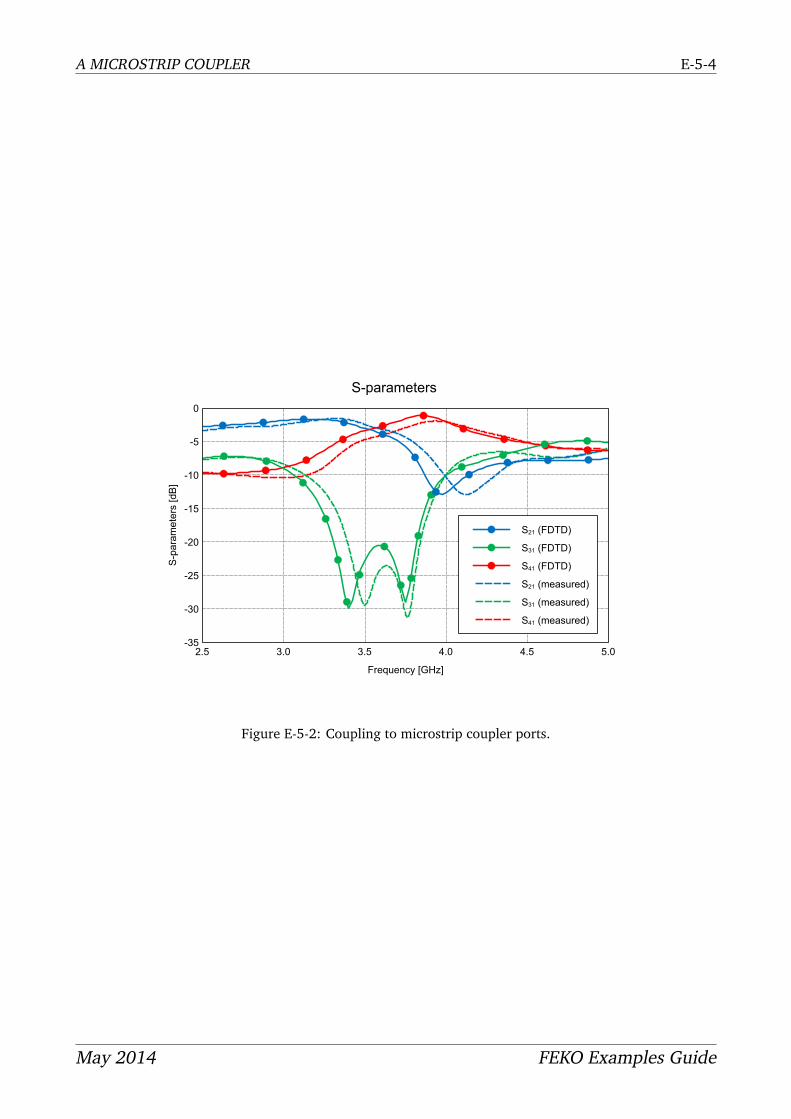
A MICROSTRIP COUPLER E-5-4
-35
-30
-25
-20
-15
-10
-5
0
2.5 3.0 3.5 4.0 4.5 5.0
S-pa
ram
eter
s [d
B]
Frequency [GHz]
S-parameters
S21 (FDTD)
S31 (FDTD)
S41 (FDTD)
S21 (measured)
S31 (measured)
S41 (measured)
Figure E-5-2: Coupling to microstrip coupler ports.
May 2014 FEKO Examples Guide

Chapter F
Bio electromagnetics

EXPOSURE OF MUSCLE TISSUE USING MOM/FEM HYBRID F-1-1
F-1 Exposure of muscle tissue using MoM/FEM hybrid
Keywords: exposure analysis, FEM/MoM hybrid method, SAR, dielectric losses
This example considers the exposure of a sphere of muscle tissue to the field created by a dipoleantenna between 0.1–1 GHz. The geometry of the example is shown in Figure F-1-1.
Figure F-1-1: Sphere of muscle tissue illuminated by a dipole antenna.
F-1.1 Dipole and muscle tissue
Note: There is an air layer used around the sphere of muscle tissue to reduce the number oftriangle elements required on the boundary between the FEM and MoM regions. This is notstrictly necessary, but if this method is not used, the resource requirements for the computation ofthe interaction between the FEM and the MoM regions would be higher without an improvementin the accuracy of the results.
Creating the model
The steps for setting up the model are as follows:
• Define the following variables:
– f_min = 100e6 (Minimum simulation frequency.)
– freq = 900e6 (Operating frequency.)
– f_max = 1e9 (Maximum simulation frequency.)
– d = 0.1 (Distance between the dipole and muscle sphere.)
– rA = 0.03 (Radius of the outer sphere.)
– rM = 0.025 (Radius of the inner sphere.)
– lambda = c0/freq (Free space wavelength.)
– wireRadius = 1e-3 (Radius of the dipole wire.)
• Create the media.
May 2014 FEKO Examples Guide

EXPOSURE OF MUSCLE TISSUE USING MOM/FEM HYBRID F-1-2
– Create a dielectric named Muscle_Parallel_Fibers_Ovine - it is available in themedia library.
– Create a dielectric named air with a relative permittivity of 1 and dielectric losstangent of zero.
• Create a sphere at the origin with a radius set to the defined variable rM. Set the label toMuscle.
• Create a sphere at the origin with a radius set to the defined variable rA. Set the label toAir.
• Union Muscle and Air.
• Use Muscle_Parallel_Fibers_Ovine for the region properties of the inside sphere.
• Set the region properties of the region between the inside and outside sphere to the dielec-tric called air.
• Set both regions to be solved using the finite element method (FEM).
• Create the line a distance of d away from the centre of the sphere. Set the Start point as(0,-lambda/4,-d) and the End point as (0,lambda/4, -d).
• Add wire vertex port on the middle of the wire.
• Add the voltage source on the port. (1 V, 0, 50 Ω)
• Set the total source power (no mismatch) to 1 W.
• Set a continuous frequency range from f_min to f_max.
Requesting calculations
In the X=0 plane, use magnetic symmetry. In the Y=0 plane, use electric symmetry. No symmetrycan be used in the Z=0 plane.
The solution requests are: Create a near field request at (0,0,0) - a single request point.
Meshing information
Use the standard auto-mesh setting. Set the wire segment radius to wireRadius.
CEM validate
After the model has been meshed, run CEM validate. Take note of any warnings and errors.Correct any errors before running the FEKO solution kernel.
F-1.2 Results
The electric field strength as a function of frequency is illustrated in Figure F-1-2.
May 2014 FEKO Examples Guide

EXPOSURE OF MUSCLE TISSUE USING MOM/FEM HYBRID F-1-3
12
15
18
21
24
27
30
0.1 0.2 0.3 0.4 0.5 0.6 0.7 0.8 0.9 1.0
E-Fi
eld
[dBV
/m]
Frequency [GHz]
Near field
Figure F-1-2: Electric field at the centre of the sphere over frequency.
May 2014 FEKO Examples Guide

MAGNETIC RESONANCE IMAGING (MRI) BIRDCAGE HEAD COIL EXAMPLE F-2-1
F-2 Magnetic Resonance Imaging (MRI) birdcage head coil ex-ample
Keywords: MRI, birdcage, S-parameters, Lua scripting, B1+
This example demonstrates the simulation of an MRI birdcage head coil with an elliptical phan-tom, shown in Figure F-2-1. The coil is a 7T highpass design with the tuning capacitors placed inthe end-ring gaps between the 16 rungs.
Figure F-2-1: Geometry for the 7T head coil with elliptical phantom.
F-2.1 Birdcage
Creating the model
This example consists of complicated geometry, the model of which is provided with the FEKOinstallation. The important details for this example are:
• The coil has an inner radius of 15 cm and an RF shield radius of 17.54 cm.
• The elliptical phantom has a major radius of 11 cm and a minor radius of 8.5 cm. Averagehead tissue properties are assigned to the phantom: εr = 36 and σ = 0.657.
• Capacitive loads (C = 4.15 pF) are added to the wire ports between the end-ring gaps onboth sides of the birdcage.
NOTE: this specific example is solved with MoM (SEP), but MoM/FEM or FDTD could also besuitable choices.
Requested calculations
A standard configuration is used to calculate the fields and currents at 300 MHz.
• The frequency (specified per configuration) for the standard configuration is set to 300 MHz.
• 2 voltage sources are added to the I and Q feed ports for the quadrature excitation. Themagnitude is set to 20 V for both and a 90 phase delay is set on the Q port.
May 2014 FEKO Examples Guide

MAGNETIC RESONANCE IMAGING (MRI) BIRDCAGE HEAD COIL EXAMPLE F-2-2
• Currents and the near fields at z = 0 are requested.
A second S-parameter configuration is used to calculated the S-parameters for the coil.
• The frequency is set to continuous (interpolated) covering 290-310 MHz.
• Both the I and Q port are set to active for the calculation.
Meshing information
In order to resolve the geometry of the coil accurately, a custom mesh size is used. The trianglelength is set to 4 cm and a local mesh size of 3 cm is set for the elliptical phantom region.
CEM validate
After the model has been meshed, run CEM validate. Take note of any warnings and errors.Correct any errors before running the FEKO solution kernel.
F-2.2 Results
The S-parameters for the head coil are shown in Figure F-2-2 as a function of frequency.
-70
-60
-50
-40
-30
-20
-10
0
290 292 294 296 298 300 302 304 306 308 310
S-pa
ram
eter
s [d
B]
Frequency [MHz]
S-parameter = S1,1S-parameter = S1,2S-parameter = S1,2S-parameter = S2,2
Figure F-2-2: S-parameters for the I and Q feed ports of the coil.
Figure F-2-3 shows the current and near field results at 300 MHz. The B1+ and ratio (B1+/B1-)plots are obtained using the MRI quantities POSTFEKO automation script, which can be found inthe same folder as the other files for this example. Other scripts and updates can be downloadedfrom www.feko.info/support/lua-scripts.
May 2014 FEKO Examples Guide

MAGNETIC RESONANCE IMAGING (MRI) BIRDCAGE HEAD COIL EXAMPLE F-2-3
Figure F-2-3: Surface currents on the coil rungs with the phantom hidden (left), B1+ field distribution atz=0 (center) and the ratio of (B1+/B1-) (right) are shown.
May 2014 FEKO Examples Guide

Chapter G
Time domain examples

TIME ANALYSIS OF THE EFFECT OF AN INCIDENT PLANE WAVE ON AN OBSTACLE G-1-1
G-1 Time analysis of the effect of an incident plane wave onan obstacle
Keywords: time domain, Fourier transform
A conducting body is placed in the path of an incident plane wave. The effect of this obstacle onthe plane wave is analysed in the time domain. The frequency domain results are first obtainedusing a wide-band simulation using traditional MoM techniques. Post processing analysis of thefrequency domain data is then performed to obtain a time response. Figure G-1-1 shows theobstacle along with the time response of the field and current components at a given time step.
Figure G-1-1: Obstacle and time domain results in the 3D view.
G-1.1 CADFEKO
Creating the model
The steps for setting up the model are as follows:
• Define the following variables:
– d = 1 (Length of the side of the cube obstacle.)
• Create a cuboid whose centre is at the origin and has a side length d.
• Define a plane wave excitation with an incident direction of θ=75 and φ=45.
• A list of discrete frequency points will be used during the simulation. Import the list ofdiscrete frequency points from the file called frequency_list.txt; this will define anarbitrarily sampled frequency span between 2.5 – 300 MHz.
Requesting calculations
Geometric symmetry may be applied to all three symmetry planes.
All surface currents should be calculated.
A near field with the following properties should be requested:
May 2014 FEKO Examples Guide
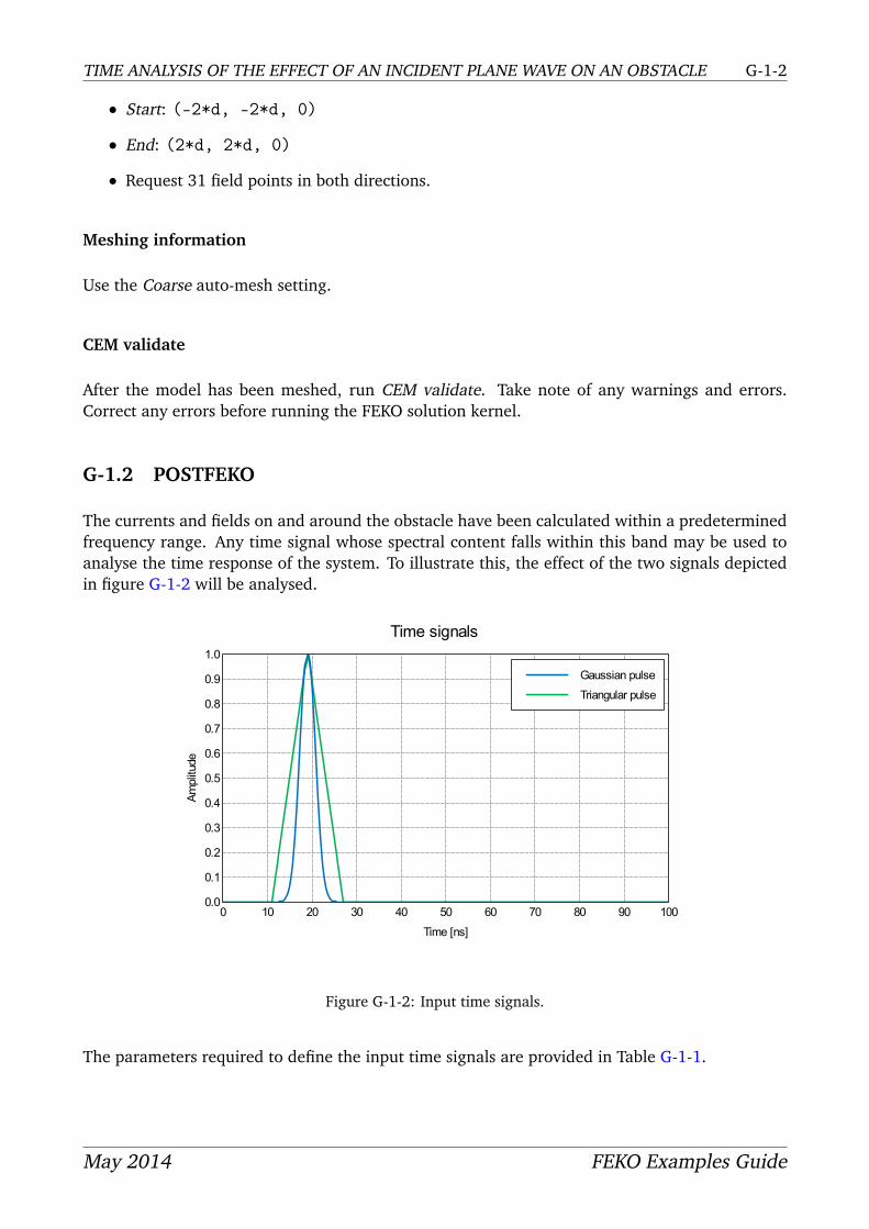
TIME ANALYSIS OF THE EFFECT OF AN INCIDENT PLANE WAVE ON AN OBSTACLE G-1-2
• Start: (-2*d, -2*d, 0)
• End: (2*d, 2*d, 0)
• Request 31 field points in both directions.
Meshing information
Use the Coarse auto-mesh setting.
CEM validate
After the model has been meshed, run CEM validate. Take note of any warnings and errors.Correct any errors before running the FEKO solution kernel.
G-1.2 POSTFEKO
The currents and fields on and around the obstacle have been calculated within a predeterminedfrequency range. Any time signal whose spectral content falls within this band may be used toanalyse the time response of the system. To illustrate this, the effect of the two signals depictedin figure G-1-2 will be analysed.
0.0
0.1
0.2
0.3
0.4
0.5
0.6
0.7
0.8
0.9
1.0
0 10 20 30 40 50 60 70 80 90 100
Ampl
itude
Time [ns]
Time signals
Gaussian pulse
Triangular pulse
Figure G-1-2: Input time signals.
The parameters required to define the input time signals are provided in Table G-1-1.
May 2014 FEKO Examples Guide

TIME ANALYSIS OF THE EFFECT OF AN INCIDENT PLANE WAVE ON AN OBSTACLE G-1-3
Property Gaussian pulse Triangular pulse
Time axis unit ns nsTotal signal duration 100 100Amplitude 1 1Pulse delay 19 19Pulse width 4 8Number of samples 400 400
Table G-1-1: Input time signal properties
G-1.3 Results
The 3D view image depicted in figure G-1-1 shows the response of the near field and currentswhen the triangular pulse is applied to the system. Animating over time is a useful means ofgaining insight into the time domain behaviour of a system.
Figure G-1-3 shows the time response of the system to the Gaussian and triangular pulses after19 ns.
Figure G-1-3: Time response to the Gaussian pulse (left) and triangular pulse (right) after 19 ns.
Time results can also be analysed on graphs. Figure G-1-4 shows the time response of the nearfield magnitude at (-2,-2,0) m to both input signals.
May 2014 FEKO Examples Guide

TIME ANALYSIS OF THE EFFECT OF AN INCIDENT PLANE WAVE ON AN OBSTACLE G-1-4
0
100
200
300
400
500
600
700
800
900
1000
0 10 20 30 40 50 60 70 80 90 100
E-Fi
eld
[mV/
m]
Time [ns]
Time responses
Response to Gaussian pulse
Response to triangular pulse
Figure G-1-4: E-Field Magnitude (X position = -2 m; Y position = -2 m; Z position = 0 m)
May 2014 FEKO Examples Guide

Chapter H
Special solution methods
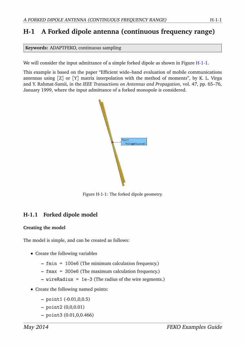
A FORKED DIPOLE ANTENNA (CONTINUOUS FREQUENCY RANGE) H-1-1
H-1 A Forked dipole antenna (continuous frequency range)
Keywords: ADAPTFEKO, continuous sampling
We will consider the input admittance of a simple forked dipole as shown in Figure H-1-1.
This example is based on the paper “Efficient wide–band evaluation of mobile communicationsantennas using [Z] or [Y] matrix interpolation with the method of moments”, by K. L. Virgaand Y. Rahmat-Samii, in the IEEE Transactions on Antennas and Propagation, vol. 47, pp. 65–76,January 1999, where the input admittance of a forked monopole is considered.
Figure H-1-1: The forked dipole geometry.
H-1.1 Forked dipole model
Creating the model
The model is simple, and can be created as follows:
• Create the following variables
– fmin = 100e6 (The minimum calculation frequency.)
– fmax = 300e6 (The maximum calculation frequency.)
– wireRadius = 1e-3 (The radius of the wire segments.)
• Create the following named points:
– point1 (-0.01,0,0.5)
– point2 (0,0,0.01)
– point3 (0.01,0,0.466)
May 2014 FEKO Examples Guide

A FORKED DIPOLE ANTENNA (CONTINUOUS FREQUENCY RANGE) H-1-2
– point4 (0,0,-0.01)
• Create 2 line primitives. One from point1 to point2, and a second from point2 topoint3.
• Apply a Copy, Copy and mirror operation, on the two lines. The mirror operation shouldbe around the UV plane.
• Create a line primitive between the named points point2 and point4. Label this line asfeed.
• Union all of the lines into a single part.
• Add a wire port to the middle of the feed wire.
• Apply a voltage excitation (1V, 0, 50 Ω) to the port.
• Set the solution frequency settings to Continuous (interpolated) range between fmin andfmax.
Requesting calculations
For this example we only wish to view the input impedance of the forked dipole. No calculationstherefore need be specifically requested.
Meshing information
Use the standard auto-mesh setting with the wire segment radius equal to wireRadius.
CEM validate
After the model has been meshed, run CEM validate. Take note of any warnings and errors.Correct any errors before running the FEKO solution kernel.
H-1.2 Results
In order to view the results for this example, we create a Cartesian graph and plot the real andimaginary parts of the input impedance of the voltage source. The input impedance is plotted inFigure H-1-2. Figure H-1-3 shows the same results over a smaller frequency band.
May 2014 FEKO Examples Guide

A FORKED DIPOLE ANTENNA (CONTINUOUS FREQUENCY RANGE) H-1-3
-10
-5
0
5
10
15
20
25
100 120 140 160 180 200 220 240 260 280 300
Adm
ittan
ce [m
S]
Frequency [MHz]
Excitation
Real
Imaginary
Figure H-1-2: Real and imaginary parts of the input admittance of the forked dipole.
-10
-5
0
5
10
15
20
25
202 203 204 205 206 207 208
Adm
ittan
ce [m
S]
Frequency [MHz]
Excitation
Real
Imaginary
Figure H-1-3: Input admittance of the forked dipole around the resonance point.
May 2014 FEKO Examples Guide

USING THE MLFMM FOR ELECTRICALLY LARGE MODELS H-2-1
H-2 Using the MLFMM for electrically large models
Keywords: MLFMM, large model, Radar cross section, trihedral
In this example we consider a single plane wave incident (from θ=60 and φ=0) on a largetrihedral. The size of the trihedral (13.5λ2 surface area) was chosen such that it can still besolved using the standard MoM. This example is large enough to demonstrate the advantage ofusing the MLFMM, but larger examples will show a proportionally larger resource savings.
Figure H-2-1 shows an illustration of the trihedral with a plane wave excitation.
Figure H-2-1: Plane wave incident on an electrically large trihedral.
H-2.1 Large trihedral
Creating the model
The steps for setting up the model are as follows:
• Define the following variables:
– lambda = 1 (Free space wavelength.)
– freq = c0/lambda (The operating frequency.)
– s = 3*lambda (Side lengths of the trihedral.)
• Create the first polygonal plate. The three corner points are (0,0,0), (s,0,0) and (0,s,0).
• Create the second polygonal plate. The three corner points are (0,0,0), (0,0,s) and (s,0,0).
• Create the third polygonal plate. The three corner points are (0,0,0), (0,s,0) and (0,0,s).
• Union the plates.
• Define a linear plane wave excitation at θ=60 and φ=45.
• Set the frequency to freq.
The model is now set up to be solved with the default MoM. The model should be set to usethe MLFMM with default values. All solution method settings, including MLFMM, are set on theSolver settings dialog.
May 2014 FEKO Examples Guide

USING THE MLFMM FOR ELECTRICALLY LARGE MODELS H-2-2
Requesting calculations
The solution requests are:
• Create a 180 vertical far field request. (-180≤θ≤180, with φ=45 and 2 steps)
Meshing information
Use the standard auto-mesh setting.
CEM validate
After the model has been meshed, run CEM validate. Take note of any warnings, notes anderrors. Please correct error before running the FEKO solution kernel.
H-2.2 Results
The runtime and memory that was used for both the MoM and MLFMM models are given inTable H-2-1. As the problem size increases, the difference will become more and more significant.Memory and other detailed information is available in the *.out file as well as in POSTFEKO’sDetails Browser.
Solution method Memory (MBytes) Runtime (seconds)
MoM 487 146MLFMM 165 53
Table H-2-1: Memory and runtime requirements for the Mom and MLFMM models
Figure H-2-2 compares the results obtained with the MLFMM with those obtained with the MoM.
May 2014 FEKO Examples Guide

USING THE MLFMM FOR ELECTRICALLY LARGE MODELS H-2-3
051015202530
030
60
90
120
150180
210
240
270
300
3300
Radar cross section (RCS)
MoM
MLFMM
Figure H-2-2: Bistatic RCS of a trihedral. Comparison of the MLFMM and MoM results.
May 2014 FEKO Examples Guide

HORN FEEDING A LARGE REFLECTOR H-3-1
H-3 Horn feeding a large reflector
Keywords: Waveguide, horn, reflector, PO, MLFMM, aperture source, spherical mode source,equivalent source, decouple, far field
A cylindrical horn is excited with a waveguide port is used to feed a parabolic reflector at12.5 GHz. The reflector is electrically large (diameter of 36 wavelengths) and well separatedfrom the horn. An illustration of the model is shown in figure H-3-1. This example illustratesseveral of the techniques available in FEKO to reduce the required resources for electrically largemodels.
Figure H-3-1: Illustration of a circular horn and parabolic dish reflector.
It is important to understand the problem to be solved and the approximations being made toreduce the required resources. Employ the following techniques to reduce the required resources:
• Use the multilevel fast multipole method (MLFMM) instead of the method of moments(MoM) for electrically large models. The required memory are reduced considerably byusing MLFMM. The MLFMM solution is used as the reference solution in the results section(H-3.7).
• Large element physical optics (LE-PO) used on sub parts of the model.
• Subdivide the problem and use an equivalent source. Possible equivalent sources are:
– Aperture source - using the equivalence principle, a region can be replaced by equiv-alent electric and magnetic field sources on the boundary of the region.
– Spherical modes source - the far field can also be used as an impressed source.
H-3.1 MoM horn and LE-PO reflector
The first example creates the horn and the dish. Simulate the horn using the method of moments(MoM) and the dish reflector using large element physical optics (LE-PO).
May 2014 FEKO Examples Guide

HORN FEEDING A LARGE REFLECTOR H-3-2
Creating the model
The model is created in two parts; create the horn first and second the parabolic dish. Start bydefining the following variables.
• freq = 12.5e9 (The operating frequency.)
• lam = c0/freq (Free space wavelength.)
• lam_w = 0.0293 (The guide wavelength.)
• h_a = 0.51*lam (The waveguide radius.)
• h_b0 = 0.65*lam (Flare base radius.)
• h_b = lam (Flare top radius.)
• h_l = 3.05*lam (Flare length.)
• ph_centre = -2.6821e-3 (Horn phase centre.)
• R = 18*lam (Reflector radius.)
• F = 25*lam (Reflector focal length.)
• w_l = 2*lam_w (The waveguide length.)
The steps for creating the horn are as follows:
• Create a cylinder along the Z axis with the base centre at (0,0,-w_l-h_l), a radius h_aand a height w_l. Label the cylinder waveguide.
• Create a cone with a base centre (0,0,-h_l), a base radius h_b0, a height h_l and a topradius h_b. Label the cone flare.
• Union the two parts and then simplify the resulting union. Rename the new part to horn.
• Delete the face on the end of the horn.
• Rotate the horn with -90 after setting the axis direction to (0,1,0).
• Set a local mesh size of lam/20 on the face at the back of the waveguide section. Create awaveguide port on the same face.
• Add a waveguide excitation on the waveguide port (Excite the fundamental mode - use thedefault settings).
The horn is now complete. The next step is to create the parabolic reflector.
• Create a paraboloid at (0,0,F) with radius R and depth -F.
Label the paraboloid reflector.
• Rotate the reflector with -90 after setting the axis direction to (0,1,0).
May 2014 FEKO Examples Guide

HORN FEEDING A LARGE REFLECTOR H-3-3
• Set the face properties of the reflector to use Large element PO - always illuminated, duringthe solution.
• Decouple the MoM and LE-PO by enabling the Decouple PO and MoM solutions option onthe High frequency tab under Solve/Run→ Solver settings.
• Set a magnetic plane of symmetry at z=0 and an electric plane of symmetry at Y=0.
• Set the frequency to freq.
Requesting calculations
Create a full 3D far field request with an increment of 5 for θ over the range -180≤θ≤180 andan increment of 5 for φ over the range 0≤φ≤180. On the Advanced tab, select continuousfar to be calculated. Spatially continuous far field allow the far field to be re-sampled to anyresolution in POSTFEKO.
Meshing information
Use the coarse auto-mesh setting. Reduce simulation time in this example by using the coarsemesh setting. The standard mesh setting is recommended in general.
CEM validate
After the model has been meshed, run CEM validate. Take note of any warnings and errors.Correct any errors before running the FEKO solution kernel.
Save the file and run the solver. Note that this is a large simulation and may take a relatively longtime to complete. The model that has been created will be referred to as the “original” modelthroughout the rest of this example.
H-3.2 MLFMM horn and PO reflector
For the second example, simulate the horn using the MLFMM and the dish reflector using physicaloptics (PO).
Creating the model
The steps for setting up the model are as follows:
• Open the original model and save it under a new name.
• Solve the model with the multilevel fast multipole method (MLFMM).
• Couple the MLFMM and PO by enabling the Couple PO and MoM/MLFMM solutions (iter-ative technique) option on the High frequency tab under Solve/Run→ Solver settings.
May 2014 FEKO Examples Guide

HORN FEEDING A LARGE REFLECTOR H-3-4
• Set the face properties of the reflector to use PO - always illuminated, during the solution.
Note that a notice will be encountered when running the solution as result of using symmetry inconjunction with the MLFMM. Using symmetry will not lead to reduction of memory or run-time,as only the geometry is mirrored for a model solved by the MLFMM.
Requesting calculations
Ensure that the 3D far field is still requested from the previously generated model. Save the fileand run the solver.
H-3.3 MLFMM horn and LE-PO reflector
For the third example, simulate the horn using the MLFMM and the dish reflector using largeelement physical optics (LE-PO).
The steps for setting up the model are as follows:
• Open the original model and save it under a new name.
• Solve the model with the multilevel fast multipole method (MLFMM).
• Couple the MLFMM and LE-PO by enabling the Couple PO and MoM/MLFMM solutions(iterative technique) option on the High frequency tab under Solve/Run→ Solver settings.
• Set the face properties of the reflector to use Large element PO - always illuminated, duringthe solution.
Note that a notice will be encountered when running the solution as result of using symmetry inconjunction with the MLFMM. Using symmetry will not lead to reduction of memory or run-time,as only the geometry is mirrored for a model solved by the MLFMM.
Requesting calculations
Ensure that the 3D far field is still requested from the previously generated model. Save the fileand run the solver.
H-3.4 Generate equivalent aperture and spherical mode sources using onlythe horn
The model is now simplified by simulating the horn by itself. A set of near field points arecalculated around the horn and then used as a source for the reflector.
May 2014 FEKO Examples Guide

HORN FEEDING A LARGE REFLECTOR H-3-5
Creating the model
The model is created by saving the previous model with a new name and making the requiredchanges. First we delete the dish from the original model and create a model containing only thehorn. The near and far field information is calculated and saved to a file.
The steps for setting up the model containing only the horn are as follows:
• Open the original model and save it under a new name.
• Remove the reflector from the model.
Requesting calculations
Request a 3D far field with an origin at (0, 0, 0); -180≤θ≤180 in θ=5 increments; 0≤φ≤180
in φ=5 increments. This is the default set of values when 3D pattern is selected on the dialog.On the Advanced tab, enable the option to Calculate continuous far field data and also Calculatespherical expansion mode coefficients. This file will be stored with a *.sph extension.
Create a spherical near field request with its origin at (w_l,0,0), radius of 1.3*w_l, 0≤θ≤180,0≤φ≤360 and an increment of 5 for θ and φ. Change the check box setting so that the nearfield is not sampled on the edges. Sampling on the edges would create duplicate request pointsat 0 and 360 and also at the poles of the spherical coordinate system. Ensure that the Exportfields to ASCII file is checked on the Advanced tab of the Near field request dialog - this saves theelectric near fields to a *.efe file and the magnetic near fields to a *.hfe file.
Meshing has already been set up and nothing should be changed. Save the file and run the solver.Once the simulation has completed, the model containing on the reflector can be constructed.
H-3.5 Aperture excitation and LE-PO reflector
The steps for setting up the model containing the reflector and equivalent aperture source are asfollows:
• Open the original model and save it under a new name.
• Remove the waveguide excitation and port.
• Remove the horn from the model.
• Create a new aperture excitation. Set the position of the workplane equal to (w_l,0,0).Enter the name of the *.efe and *.hfe in the Source group box. The coordinate systemis a spherical coordinate system with radius 1.3*w_l and the number of θ and φ points isequal to 36 and 71 respectively.
Requesting calculations
Ensure that the 3D far field is still requested from the previously generated model.
Save the file and run the solver.
May 2014 FEKO Examples Guide

HORN FEEDING A LARGE REFLECTOR H-3-6
H-3.6 Spherical excitation and LE-PO reflector
In this model, the far field that was stored in the *.sph file from the horn model is used. As forthe previous model when the near fields were used, the horn is removed from the full model andreplaced by an equivalent source.
Creating the model
The original model is opened again and saved with a different name. The horn is removed and anew excitation is created for the dish.
The steps for setting up the model containing the reflector and equivalent spherical mode sourceare as follows:
• Open the original model and save it under a new name.
• Remove the waveguide excitation and port.
• Remove the horn from the model.
• Create a new spherical mode source at (0,0,0). Select the *.sph file that has been createdduring the previous simulation.
Requesting calculations
No calculation requests need to be created since the far field request was created in the originalmodel and it has not been removed.
Save the file and run the solver.
H-3.7 Comparative results
The required resources (memory and CPU time) is listed in Table H-3-1. It is clear that therequired resources are decreased by using approximations. By simply using LE-PO as solutionmethod for the reflector, the memory requirement and solution time is reduced by several ordersof magnitude. By sub-dividing the model into equivalent source models, the resource require-ments can be reduced even further.
The differences in the results is shown in figure H-3-2 and H-3-3 respectively.
We can see there is excellent comparison between the results. Difference observed in the resultsare due to coupling between the horn and reflector only taken into account for MLFMM solution.Although there is no restriction on the size of LE-PO triangles, the geometry must be accuratelymeshed. For example, had a flat plate been used, only two triangles would have been requiredto obtain the same results.
May 2014 FEKO Examples Guide

HORN FEEDING A LARGE REFLECTOR H-3-7
Table H-3-1: Comparison of resources using different techniques for large models.
Model RAM Time [s] Total Time [s]
MLFMM (benchmark) 6.300 Gb 1805 1805MLFMM Horn + PO Reflector 700 Mb 4359 4359MLFMM Horn + LE-PO Reflector 473 Mb 998 998MoM Horn + LE-PO Reflector 208 Mb 98 98Generate AP & AS source data 20 Mb 36AP source + LE-PO Reflector 61 Mb 125 161Spherical source + LE-PO Reflector 36 Mb 12 48
-40
-20
0
20
40
60
-90 -60 -30 0 30 60 90
Gai
n [d
Bi]
Theta [deg]
Far field
MLFMM
MLFMM + PO
MLFMM + LE-PO
MoM + LE-PO
Aperture + LE-PO
Spherical + LE-PO
Figure H-3-2: Gain of the reflector antenna calculated using different techniques over a 180 degree angle.
May 2014 FEKO Examples Guide

HORN FEEDING A LARGE REFLECTOR H-3-8
-20
-10
0
10
20
30
40
80 81 82 83 84 85 86 87 88 89 90
Gai
n [d
Bi]
Theta [deg]
Far field
MLFMM
MLFMM + PO
MLFMM + LE-PO
MoM + LE-PO
Aperture + LE-PO
Spherical + LE-PO
Figure H-3-3: Gain of the reflector antenna calculated using different techniques - main lobe.
May 2014 FEKO Examples Guide

OPTIMISE WAVEGUIDE PIN FEED LOCATION H-4-1
H-4 Optimise waveguide pin feed location
Keywords: waveguide, NGF, optimisation, grid search
In practice, a waveguide can be fed using a pin placed a quarter of a waveguide wavelengthfrom a terminated end of the waveguide. This can be a difficult position to determine for ar-bitrary waveguide cross-sections, since the waveguide wavelength is not always known. Thisexample will demonstrate how to use an optimisation grid search and the NGF solution settingsto efficiently analyse the effect of the pin offset on the reflection coefficient.
Figure H-4-1: 3D view of a waveguide fed with a pin feed.
H-4.1 Pin fed waveguide
Creating the model
The steps for setting up the model are as follows:
• Set the model unit to millimetres.
• Define the following variables:
– freq = 10e9 (Centre frequency.)
– lambda = c0/freq*1e3 (Free space wavelength in millimetres.)
– n = 1 (Feed pin position index.)
– pin_step_size = lambda/32 (Distance between pin positions.)
– pin_length = 0.9*lambda/4 (Length of pin feed monopole.)
– pin_offset = pin_step_size*n (Pin offset from waveguide tip.)
– radius = 0.1 (Radius of pin wires.)
– waveguide_length = lambda*2 (Length of waveguide section.)
– wr90_height = 10.16 (Waveguide height for WR90 (X-Band).)
– wr90_width = 22.86 (Waveguide width for WR90 (X-Band).)
• Create a cuboid labelled waveguide. It is created with the Base centre, width, depth,height definition method. The base centre is at (0,0,0) and with
May 2014 FEKO Examples Guide

OPTIMISE WAVEGUIDE PIN FEED LOCATION H-4-2
– width: wr90_width
– depth: waveguide_length
– height: wr90_height
• Set the region of the waveguide to free space.
• Create lines that will be used to imprint vertices on the mesh.
– Create a line labelled imprinted_edge_1 starting at (0, -waveguide_length/2,0) and ending at (0, -waveguide_length/2+pin_step_size, 0).
– Copy and translate the line from (0,0,0) to (0, 2*pin_step_size, 0) a number of 7times.
• Union all geometry and label it waveguide_perforated.
• Activate NGF and set waveguide_perforated as a static part. You’ll see the NGF icon inthe tree next to the part. It will prevent any changes to the static part of the model.
• Create the feed pin using a line:
– start point: (0, pin_offset, 0)
– end point: (0, pin_offset, pin_length)
– workplane origin: (0, -waveguide_length/2, 0)
• Add a segment port at the connection point between the feed and the waveguide floor.
• Place a waveguide port at the other end of the waveguide. This will absorb the powerinjected by the pin feed.
• Apply a voltage excitation (1V, 0, 50 Ω) to the wire port.
• Set the frequency to freq.
Requesting calculations
Magnetic symmetry exists in the X=0 plane, but no performance gain is experienced when usedin conjunction with the NGF.
No solution requests are required since the input impedance and reflection coefficient is alwaysavailable as output for all voltage sources in the model.
Setting up optimisation
• An optimisation search is added with the Grid search method and 15 default points.
• The following parameters are set:
– n (min 1; max 15; grid points 15)
• Set an Impedance goal to minimise the magnitude of the reflection coefficient.
May 2014 FEKO Examples Guide

OPTIMISE WAVEGUIDE PIN FEED LOCATION H-4-3
Meshing information
Use the fine auto-mesh setting and set the wire segment radius to radius.
CEM validate
After the model has been meshed, run CEM validate. Take note of any warnings and errors.Correct any errors before running OPTFEKO.
H-4.2 Results
The first time the solver is run, the full calculation needs to be performed. The solution to thestatic domain is stored in a file, which can be reused in subsequent simulations. By storing thesolution to the static domain, which in this case is the waveguide, FEKO only needs to calculatethe effect of the feed pin location in further simulations.
The resource requirements for each iteration are given in Table H-4-1. Note that the first runtook significantly longer than the rest. This effect will become more pronounced as the size ofthe static domain increases relative to the dynamic domain.
Iteration Memory (MBytes) Runtime (seconds)
1 231.780 87.42 231.863 15.73 231.863 10.64 231.863 9.85 231.863 9.46 231.863 9.37 231.863 9.58 231.863 9.69 231.863 9.710 231.863 9.311 231.863 9.312 231.863 9.113 231.863 9.514 231.863 10.015 231.863 9.0
Table H-4-1: Comparison of resource requirements for each iteration.
The port is optimally matched when the magnitude of the reflection coefficient is as small aspossible or the input impedance is equal to 50 Ω. On the Smith chart depicted in Figure H-4-2,we can see this condition is met roughly at iteration 6. This corresponds to a feed pin positiongiven by Eq. H-4-1
pin_o f f set ≈ 6× pin_step_size =6
32λ. (H-4-1)
May 2014 FEKO Examples Guide

OPTIMISE WAVEGUIDE PIN FEED LOCATION H-4-4
-10
-5
-3
-2
-1.4-1-0.7
-0.5-0.4
-0.3
-0.2
-0.1
0.1
0.2
0.3
0.40.5
0.7 1 1.4
2
3
5
10
0.1
0.2
0.3
0.4
0.5
0.7 1
1.4 2 3 5 10
S-parameter
Figure H-4-2: Smith chart showing the reflection coefficient for each feed pin position.
May 2014 FEKO Examples Guide

Chapter I
User interface tools

POSTFEKO APPLICATION AUTOMATION I-1-1
I-1 POSTFEKO Application automation
Keywords: application automation, API, POSTFEKO, online help, scripting, forms, reporting
Application automation is a tool that can increase productivity when dealing with predictableand repeatable POSTFEKO sessions. This example will illustrate how an automation script canbe used to configure a session and export a report that highlights the antenna properties of themodel.
It will be illustrated that a script can be used on various models with repeatable results. Fig-ure I-1-1 shows equivalent pages for two different antenna types.
Figure I-1-1: Results of the automatic report generation.
Note that the base language for the automation interface is Lua. For a complete guide on theLua language, we refer you to the official Lua Reference Manual (www.lua.org/manual/5.1/)and Programming introduction (www.lua.org/pil/). Another useful resource is the communitymaintained Wiki that is available on the internet at lua-users.org/wiki/.
For documentation and examples on how to use the automation API, see the online help bypressing on the help button in the script editor.
May 2014 FEKO Examples Guide

POSTFEKO APPLICATION AUTOMATION I-1-2
I-1.1 The models
Two models are included with this example that will provide the content of the POSTFEKOsessions. Assumptions are made about both models. For instance:
• It is assumed that the first configuration will contain 3D far field data.
• It is assumed that the far field can be wrapped in the θ direction.
• It is assumed that there is a φ angle calculated at φ=0 and at φ=90. This also impliesthat the main direction of radiation is in the positive Z axis.
Apart from these assumptions, any antenna geometry can be used as an input. The script can beadapted to iterate over multiple models or to display different properties of interest.
I-1.2 Exercises
As an exercise, modify the script from section I-1.3 to:
• change the rendering of the mesh to be 60% opaque.
• Automatically generate reports for all of the models in the modelName list.
• Save the sessions under unique names.
Another exercise that could be useful to try is to reproduce figure I-1-2. It is recommended towrite a new script and make use of the documentation for this exercise. Export the graph to a*.pdf file and save the session.
-50-40-30-20-100
030
60
90
120
150180
210
240
270
300
3300
Total Gain (Phi = 0 deg)
Normalised Gain Patterns
Horn Patch
Figure I-1-2: Gain patterns for both antenna models.
May 2014 FEKO Examples Guide

POSTFEKO APPLICATION AUTOMATION I-1-3
I-1.3 The script
generate_antenna_report.lua
--[[AUTOMATIC QUICK REPORT GENERATION FOR ANTENNA PATTERN ANALYSIS==============================================================This script loads the specified model. It then creates variousviews and graphs that display the far field pattern. Theseviews are then exported to a PDF report]]--
modelName = modelName[1] = "Horn"modelName[2] = "Patch"
-- Get user input through Formsform = pf.Form.New("Select model")comboBox = pf.FormComboBox.New("Model name", modelName)form:Add(comboBox)form:Run()index = comboBox.Index
app = pf.GetApplication()app:NewProject()app:OpenFile(modelName[index]..".fek")
selectedModel = app.Models[modelName[index]]selectedConfig1 = selectedModel.Configurations[1]
ffData = selectedConfig1.FarFields[1] -- This is a handle on the far field data itself
view3D = app.Views[1]ffPlot = view3D.Plots:Add(ffData)ffPlot.Label = "ff3D"ffPlot.Quantity.ValuesScaledToDB = true
view3D_top = view3D:Duplicate()view3D_top:SetViewDirection(pf.Enums.ViewDirectionEnum.Top)
view3D_right = view3D:Duplicate()view3D_right:SetViewDirection(pf.Enums.ViewDirectionEnum.Right)
view3D_front = view3D:Duplicate()view3D_front:SetViewDirection(pf.Enums.ViewDirectionEnum.Front)
polarGraph = app.PolarGraphs:Add()ffTracePhi_00 = polarGraph.Traces:Add(ffData)ffTracePhi_00.IndependentAxis = "Theta (wrapped)"ffTracePhi_00.Quantity.ValuesScaledToDB = trueffTracePhi_90 = polarGraph.Traces:Add(ffData)ffTracePhi_90.IndependentAxis = "Theta (wrapped)"ffTracePhi_90.Quantity.ValuesScaledToDB = trueffTracePhi_90:SetFixedAxisValue(ffTracePhi_90.FixedAxes[2],90,"deg")polarGraph:ZoomToExtents()polarGraph.Title.Text = "Gain"polarGraph.Legend.Position = pf.Enums.GraphLegendPositionEnum.OverlayTopRightpolarGraph.BackColour = pf.Enums.ColourEnum.LightGreypolarGraph:Restore()
quickReport = app:CreateQuickReport(modelName[index].."AntennaQuickReport",pf.Enums.ReportDocumentTypeEnum.PDF)
quickReport.DocumentHeading = modelName[index]..[[ Antenna:Automated Quick Report]]quickReport:SetPageTitle(view3D.WindowTitle, "Isometric View")quickReport:SetPageTitle(view3D_top.WindowTitle, "Top View")quickReport:SetPageTitle(view3D_right.WindowTitle, "Right View")quickReport:SetPageTitle(view3D_front.WindowTitle, "Front View")quickReport:SetPageTitle(polarGraph.WindowTitle, "Theta Cuts")quickReport:Generate()
May 2014 FEKO Examples Guide

Chapter J
Index

Index
AADAPTFEKO . . . . . . . . . . . . . . . . . . . . . . . . . . . . . . . . H-1-1adaptive sampling . . . . . . . . . . . . . . . . . . . . . . . . . . H-1-1antenna placement . . . . . . . . . . . . . . . . . . . . . . . . . .B-1-1API . . . . . . . . . . . . . . . . . . . . . . . . . . . . . . . . . . . . . . . . . . I-1-1application
antenna analysis . . . . . . . . . . A-1-1, A-4-1, A-5-1,A-7-1, A-8-1, A-9-1, A-11-1, A-12-1, D-4-1,E-3-1, H-1-1, H-3-1
antenna optimisation . . . . . . . . . . . . . . . . . . . A-6-1antenna placement . . . . . . . . . . . . . . . . . . . . . B-1-1cable analysis . . . . . . . . . . . . . . . . . . . . . . . . . . .D-2-1EMC . . . . . . . . . . . . . . . . . . . . . .D-1-1, D-2-1, D-3-1exposure analysis . . . . . . . . . . . . . . . . . . . . . . . F-1-1lens antenna . . . . . . . . . . . . . . . . . . . . . . . . . . A-13-1microstrip coupler analysis . . . . . . . . . . . . . . E-5-1microstrip filter analysis . . . . . . . . . . . . . . . . .E-1-1SAR . . . . . . . . . . . . . . . . . . . . . . . . . . . . . . . . . . . . .F-1-1time domain analysis . . . . . . . . . . . . . . . . . . . G-1-1waveguide analysis . . . . . . . . . . . . . . E-2-1, H-4-1
application automationForms . . . . . . . . . . . . . . . . . . . . . . . . . . . . . . . . . . . I-1-1POSTFEKO . . . . . . . . . . . . . . . . . . . . . . . . . . . . . . I-1-1
array . . . . . . . . . . . . . . . . . . . . . . . . . . . . . . . . . . . . . . . A-7-1
Bbirdcage . . . . . . . . . . . . . . . . . . . . . . . . . . . . . . . . . . . . .F-2-1
Ccable analysis . . . . . . . . . . . . . . . . . . . . . . . . . . . . . . . D-2-1cable modelling . . . . . . . . . . . . . . . . . . . . . . . . . . . . .D-2-1CFIE . . . . . . . . . . . . . . . . . . . . . . . . . . . . . . . . . . . . . . . . B-1-1characteristic modes . . . . . . . . . . . . . . . . . . . . . . . A-15-1continuous frequency . . . . . . . . . . . . . . . . . . . . . . . H-1-1coupling . . . . . . . . . . . . . . . . B-1-1, B-2-1, B-3-1, D-2-1current . . . . . . . . . . . . . . . . . . . . . . . . . . . . . . . . . . . . . A-4-1
Ddielectric losses . . . . . . . . . . . . . . . . . . . . . . . . . . . . . .F-1-1dielectric resonator antenna (DRA) . . . . . . . . .A-12-1dielectric solid . . . . . . . . . . . . . . . . . . . . . . . A-2-1, C-2-1dielectric substrate . . . . . . . . . . . . . . . . . . . A-8-1, A-9-1dipole . . . . . . . . . . . . . . . . . . . . . . . . . . . . . . . . A-1-1, A-7-1
forked . . . . . . . . . . . . . . . . . . . . . . . . . . . . . . . . . .H-1-1ideal lumped element matching . . . . . . . . . E-3-1
near a cube . . . . . . . . . . . . . . . . . . . . . . . . . . . . . A-2-1near a dielectric sphere . . . . . . . . . . . . . . . . . .F-1-1near a large metal plate . . . . . . . . . . . . . . . . .A-3-1
Eedge port . . . . . . . . . . . . . . . . . . . . . . . . . . . . . . . . . . . A-9-1electrically large model . B-1-1, B-2-1, B-3-1, H-2-1EMC . . . . . . . . . . . . . . . . . . . . . . . . . . D-1-1, D-2-1, D-3-1excitation
edge excitation . . . . . . . . . . . . . . . . . . . E-1-1, E-5-1FEM current source . . . . . . . . . . . . . . . . . . . .A-12-1FEM modal source . . . . . . . . . . . . . . . . . . . . .A-12-1impressed field distribution . . . . . . . . . . . . A-11-1microstrip feed . . . . . . . . . . . . . . . . . . . . . . . . . A-9-1pin feed . . . . . . . . . . . . . . . . . . . . . . . . . . . . . . . A-11-1plane wave . C-1-1, C-2-1, C-3-1, C-4-1, D-1-1,
D-3-1, H-2-1radiation pattern point source . . .A-13-1, B-3-1voltage on an edge . . . . . . . . . . . . . . . . . . . . . .A-9-1voltage source . . . . . . . . . . . . . . . . . A-16-1, A-17-1waveguide feed . . . . . . . . . . . . . . . . . A-11-1, E-2-1
exposure analysis . . . . . . . . . . . . . . . . . . . . . . . . . . . . F-1-1
Ffar field A-1-1, A-3-1, A-4-1, A-7-1, A-11-1, A-12-1,
A-16-1, A-17-1far field data file . . . . . . . . . . . . . . . . . . . . . .B-2-1, B-3-1FDTD . . . . . . . . . . . . . . . . . . . . . . . . . .A-3-1, A-8-1, E-5-1feed network . . . . . . . . . . . . . . . . . . . . . . . . . . . . . . . . E-4-1FEM current source . . . . . . . . . . . . . . . . . . . . . . . . A-12-1FEM modal source . . . . . . . . . . . . . . . . . A-12-1, A-12-3FEM/MoM hybrid . . . . . . . . . . . . . . . . . . . . . . . . . . . F-1-1finite array . . . . . . . . . . . . . . . . . . . . . . . . . . . . . . . . A-17-1finite conductivity . . . . . . . . . . . . . . . . . . . . . . . . . . .D-1-1finite ground plane . . . . . . . . . . . . . . . . . . . . . . . . . .A-4-1
Ggeometrical optics . . . . . . . . . . . . . . . . . . . . . . . . . A-13-1GO . . . . . . . . . . . . . . . . . . . . . . . . . . . . . . . . . . . . . . . . . A-3-1
Hhalf-wavelength dipole . . . . . . . . . . . . . . . . . . . . . . A-1-1helix antenna . . . . . . . . . . . . . . . . . . . . . . . . . . . . . . . B-2-1HOBF . . . . . . . . . . . . . . . . . . . . . . . . . . . . . . . . . . . . . . .A-3-1horn antenna . . . . . . . . . . . . . . . . . . . . . . . A-11-1, B-3-1
I-1

Iideal matching . . . . . . . . . . . . . . . . . . . . . . . . . . . . . . E-3-1ideal receiving antenna . . . . . . . . . . . . . . . B-2-1, B-3-1infinite ground . . . . . . . . . . . . . . . . . . . . . . A-5-1, A-12-1infinite planar Green’s function . . . . . . A-5-1, A-9-1,
A-12-1input impedance . . . . . . . . . . . . . A-1-1, A-12-1, E-1-1
Llens antenna . . . . . . . . . . . . . . . . . . . . . . . . . . . . . . .A-13-1lossy metal . . . . . . . . . . . . . . . . . . . . . . . . . . . . . . . . . .A-2-1
Mmagnetic field probe . . . . . . . . . . . . . . . . . . . . . . . . D-3-1Magnetic Resonance Imaging . . . . . . . . . . . . . . . . F-2-1materials
dielectric solid . . . . . . . . . . . A-2-1, A-13-1, C-2-1lossy metal . . . . . . . . . . . . . . . . . . . . . . A-2-1, D-1-1PEC . . . . . . . . . . . . . . . . . . . . . . . . . . . . . . . . . . . . A-2-1
method of moments . . . .A-1-1, A-2-1, D-1-1, D-4-1,F-2-1
microstrip . . . . . . . . . . . . . . . . . . . . . . . . . . . . A-8-1, A-9-1feed line . . . . . . . . . . . . . . . . . . . . . . . . . . . . . . . . A-9-1
microstrip coupler . . . . . . . . . . . . . . . . . . . . . . . . . . .E-5-1microstrip feed . . . . . . . . . . . . . . . . . . . . . . . . . . . . . .A-8-1microstrip filter . . . . . . . . . . . . . . . . . . . . . . . . . . . . . E-1-1MIMO . . . . . . . . . . . . . . . . . . . . . . . . . . . . . . . . . . . . . A-15-1MLFMM . . . . . . . . . . . . . . . . . . . . . . . . . . . . . B-1-1, H-2-1MoM . . . . . . . . . . . . . . . . . . . . . . . . . . . . . . . . . . . . . . . A-3-1monopole antenna . . . . . . . . . . . . . . . . . . . . . . . . . . A-4-1MRI . . . . . . . . . . . . . . . . . . . . . . . . . . . . . . . . . . . . . . . . . F-2-1
Nnear fields . . . . . . . . . . . . . . . . . . . . . . . . . . . . . . . . . . D-1-1non-radiating network . . . . . . . . . A-7-1, E-3-1, E-4-1
Oonline help . . . . . . . . . . . . . . . . . . . . . . . . . . . . . . . . . . I-1-1optimisation . . . . . . . . . . . . . . . . . . . . . . . . . A-6-1, H-4-1
Ppatch . . . . . . . . . . . . . . . . . . . . . . . . . . . . . . . . . . . . . . . E-4-1patch antenna . . . . . . . . . . . . . . . . . . . . . . . . A-8-1, A-9-1PEC . . . . . . . . . . . . . . . . . . . . . . . . . . . . . . . . . . . . . . . . .A-2-1pin feed . . . . . . . . . . . . . . . . . . . . . . . . . . . . .A-8-1, A-11-1planar multilayer substrate (Green’s function) A-8-1plane wave . . . . . . . . . . . . . . . . . . . .C-1-1, C-2-1, D-1-1PO . . . . . . . . . . . . . . . . . . . . . . . . . . . . . . . . . . . . . . . . . .A-3-1polygon plate . . . . . . . . . . . . . . . . . . . . . . . . . . . . . . . C-1-1proximity coupling . . . . . . . . . . . . . . . . . . . . . . . . . . A-9-1pulse shape . . . . . . . . . . . . . . . . . . . . . . . . . . . . . . . . . G-1-1
Rradiation pattern . . . . . A-1-1, A-4-1, A-11-1, A-13-1
radiation pattern point source . . . . . . . . . . . . . . . B-3-1ray tracing . . . . . . . . . . . . . . . . . . . . . . . . . . . . . . . . .A-13-1RCS (radar cross section) . . . . . . . . . . . . . . . . . . . C-2-1real ground . . . . . . . . . . . . . . . . . . . . . . . . . . . . . . . . . A-5-1reporting . . . . . . . . . . . . . . . . . . . . . . . . . . . . . . . . . . . . I-1-1resource requirements . . . . . . . . . . . . . . . . . . . . . . H-2-1results
continuous frequency . . . . . . . . . . . . . . . . . . . H-1-1current . . . . . . . . . . . . . . . . . . . . . . . . . . A-4-1, D-3-1far field . . . A-1-1, A-3-1, A-4-1, A-11-1, A-12-1gain . . . . . . . . . . . . . . . . . . . . . . . . . . . . . . . . . . . . A-5-1input impedance . A-1-1, A-12-1, A-14-1, E-1-1RADHAZ . . . . . . . . . . . . . . . . . . . . . . . . . . . . . . . D-4-1radiation pattern . . . . . . . . . . A-1-1, A-4-1, A-6-1RCS (Radar cross section)
bistatic . . . . . . . . . . . . . . . . . . . . . . . . . . . . . . . C-2-1monostatic . . . . . . . . . . . . . . . . . . . . . . . . . . . C-2-1
RCS (radar cross section)bistatic . . . . . . . . . . . . . . . . . . . . . . . . . . . . . . . C-1-1monostatic . . . . . . . . . . . . . . . . . . . . . . . . . . . H-2-1
reflection coefficient . . . . . . . . . . . . . .A-9-1, E-1-1S-parameters B-1-1, E-1-1, E-2-1, E-3-1, E-4-1,
E-5-1, H-4-1
SS-parameters . . . . . . . . . . . . . . . . . . . . . . . . . E-3-1, E-4-1SAR . . . . . . . . . . . . . . . . . . . . . . . . . . . . . . . . . . . . . . . . . F-1-1scripting . . . . . . . . . . . . . . . . . . . . . . . . . . . . . . . . . . . . . I-1-1shielded cable . . . . . . . . . . . . . . . . . . . . . . . . . . . . . . D-2-1shielding . . . . . . . . . . . . . . . . . . . . . . . . . . . . .D-1-1, D-3-1skin effect . . . . . . . . . . . . . . . . . . . . . . . . . . . . . . . . . . D-1-1Smith chart . . . . . . . . . . . . . . . . . . . . . . . . . . . . . . . . . A-9-1solution method
DGFM . . . . . . . . . . . . . . . . . . . . . . . . . . . . . . . . .A-17-1FDTD . . . . . . . . . . . . . . . . . . . . . A-3-1, A-8-1, E-5-1FEM/MoM . . . . . . . . . . . . . . . . . . . . . . . . . . . . . . F-1-1geometrical optics . . . . . . . . . . . . . . . . . . . . . A-13-1infinite planar Green’s function . . A-5-1, A-9-1,
A-12-1method of moments .A-1-1, A-2-1, D-1-1, F-2-1MLFMM . . . . . . . . . . . . . . . . . . . . . . . . . B-1-1, H-2-1MoM . . . . . . . . . . . . . . . . . . . . . . . . . . . . . . . . . . . A-3-1MoM/GO . . . . . . . . . . . . . . . . . . . . . . . . . . . . . . . A-3-1MoM/PO . . . . . . . . . . . . . . . . . . . . . . . . . . . . . . . A-3-1MoM/UTD . . . . . . . . . . . . . . . . . . . . . . . . . . . . . A-3-1NGF . . . . . . . . . . . . . . . . . . . . . . . . . . . . . . . . . . . .H-4-1periodic boundary conditions . . .A-16-1, C-3-1,
C-4-1planar multilayer substrate (Green’s function)
A-8-1surface equivalence principle . . . . A-2-1, A-8-1,
C-2-1, E-1-1
I-2

symmetry . . . . . . . . . . . . . . . . . . . . . . . . . . . . . . .A-9-1thin dielectric sheet approximation . . . . . .C-1-1UTD . . . . . . . . . . . . . . . . . . . . . . . . . . . . . . . . . . . . B-2-1
sphere creation . . . . . . . . . . . . . . . . . . . . . . . . . . . . . C-2-1surface equivalence principle . . . . . . . . . A-2-1, C-2-1
Tthin dielectric sheet approximation . . . . . . . . . . C-1-1time domain . . . . . . . . . . . . . . . . . . . . . . . . . . . . . . . . G-1-1Touchstone . . . . . . . . . . . . . . . . . . . . . . . . . . . E-3-1, E-4-1transmission line . . . . . . . . . . . . . . . . . . . . . . . . . . . . A-7-1trihedral reflector . . . . . . . . . . . . . . . . . . . . . . . . . . . H-2-1
UUTD . . . . . . . . . . . . . . . . . . . . . . . . . . . . . . . . . A-3-1, B-2-1
Wwaveguide . . . . . . . . . . . . . . . . . . . A-11-1, E-2-1, H-4-1waveguide modes . . . . . . . . . . . . . . . . . . . . . . . . . . . E-2-1windscreen . . . . . . . . . . . . . . . . . . . . . . . . . . . . . . . . A-14-1wires . . . . . . . . . . . . . . . . . . . . . . . . . . . . . . . . . . . . . . . A-1-1
YY-parameters . . . . . . . . . . . . . . . . . . . . . . . . . . . . . . . . E-3-1Yagi-Uda antenna . . . . . . . . . . . . . .A-5-1, A-6-1, B-2-1
ZZ-parameters . . . . . . . . . . . . . . . . . . . . . . . . . . . . . . . .E-3-1
I-3

www.feko.info • FEKO is a product of EM Software & Systems - S.A. (Pty) Ltd