Embed Size (px)
Citation preview
SLLS236F − OCTOBER 1996 − REVISED APRIL 2005
1POST OFFICE BOX 655303 • DALLAS, TEXAS 75265
Integrated Transient Voltage Suppression
ESD Protection for Bus Terminals Exceeds: ±30 kV IEC 61000-4-2, Contact Discharge ±15 kV IEC 61000-4-2, Air-Gap Discharge ±15 kV EIA/JEDEC Human Body Model
Circuit Damage Protection of 400-W Peak(Typical) Per IEC 61000-4-5
Controlled Driver Output-Voltage SlewRates Allow Longer Cable Stub Lengths
250-kbps in Electrically NoisyEnvironments
Open-Circuit Fail-Safe Receiver Design
1/4 Unit Load Allows for 128 DevicesConnected on Bus
Thermal Shutdown Protection
Power-Up/-Down Glitch Protection
Each Transceiver Meets or Exceeds theRequirements of TIA/EIA-485 (RS-485) andISO/IEC 8482:1993(E) Standards
Low Disabled Supply Current 300 µA Max
Pin Compatible With SN75176
Applications:− Industrial Networks− Utility Meters− Motor Control
description
The SN75LBC184 and SN65LBC184 are differ-ential data line transceivers in the trade-standardfootprint of the SN75176 with built-in protectionagainst high-energy noise transients. This featureprovides a substantial increase in reliability forbetter immunity to noise transients coupled to thedata cable over most existing devices. Use ofthese circuits provides a reliable low-costdirect-coupled (with no isolation transformer) dataline interface without requiring any externalcomponents.
The SN75LBC184 and SN65LBC184 can with-stand overvoltage transients of 400-W peak(typical). The conventional combination wavecalled out in IEC 61000-4-5 simulates theovervoltage transient and models a unidirectionalsurge caused by overvoltages from switching andsecondary lightning transients.
Please be aware that an important notice concerning availability, standard warranty, and use in critical applications ofTexas Instruments semiconductor products and disclaimers thereto appears at the end of this data sheet.
1
2
3
4
8
7
6
5
RREDE
D
VCCBAGND
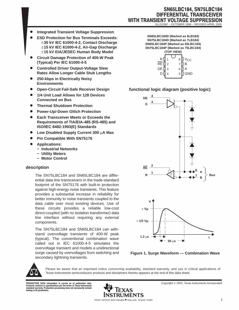
functional logic diagram (positive logic)
DE
RE
R
6
7
3
1
2
B
ABus
D4
Figure 1. Surge Waveform — Combination Wave
1.2 µs50 µs
V
t
± VP
± 1/2 VP
SN65LBC184D (Marked as 6LB184)SN75LBC184D (Marked as 7LB184)
SN65LBC184P (Marked as 65LBC184)SN75LBC184P (Marked as 75LBC184)
(TOP VIEW)
!"#$ % &'!!($ #% )'*+&#$ ,#$(-!,'&$% &!" $ %)(&&#$% )(! $.( $(!"% (/#% %$!'"($%%$#,#!, 0#!!#$1- !,'&$ )!&(%%2 ,(% $ (&(%%#!+1 &+',($(%$2 #++ )#!#"($(!%-
Copyright 2002, Texas Instruments Incorporated
SLLS236F − OCTOBER 1996 − REVISED APRIL 2005
2 POST OFFICE BOX 655303 • DALLAS, TEXAS 75265
description (continued)
A biexponential function defined by separate rise and fall times for voltage and current simulates thecombination wave. The standard 1.2 µs/50 µs combination waveform is shown in Figure 1 and in the testdescription in Figure 15.
The device also includes additional desirable features for party-line data buses in electrically noisy environmentapplications including industrial process control. The differential-driver design incorporates slew-rate-controlledoutputs sufficient to transmit data up to 250 kbps. Slew-rate control allows longer unterminated cable runs andlonger stub lengths from the main backbone than possible with uncontrolled and faster voltage transitions. Aunique receiver design provides a fail-safe output of a high level when the inputs are left floating (open circuit).The SN75LBC184 and SN65LBC184 receiver also includes a high input resistance equivalent to one-fourth unitload allowing connection of up to 128 similar devices on the bus.
The SN75LBC184 is characterized for operation from 0°C to 70°C. The SN65LBC184 is characterized from−40°C to 85°C.
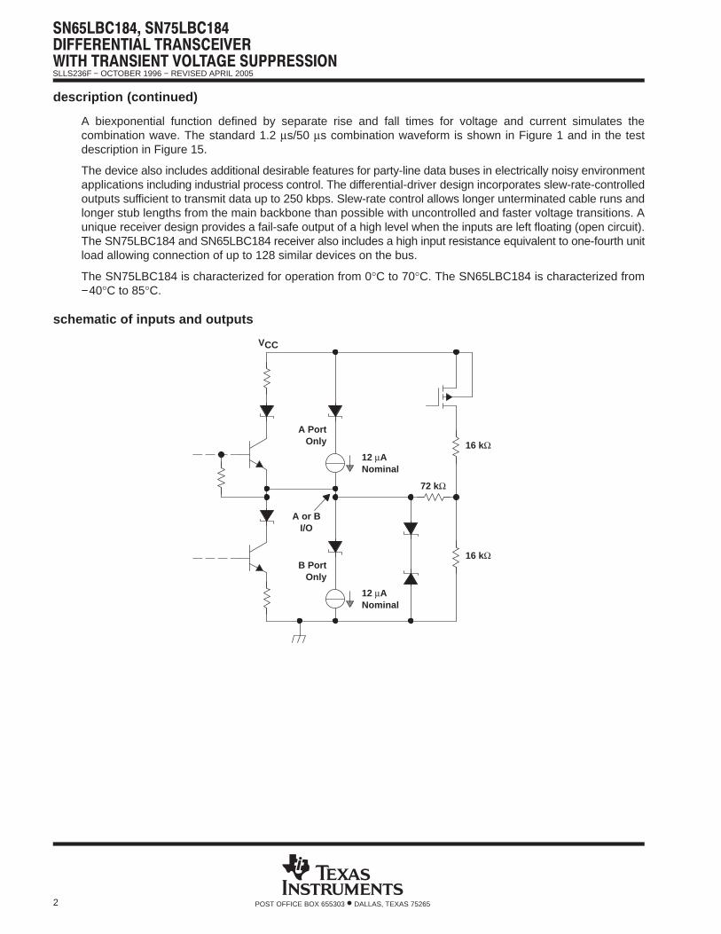
schematic of inputs and outputs
A PortOnly
12 µANominal
A or BI/O
B PortOnly
12 µANominal
72 kΩ
16 kΩ
16 kΩ
VCC
SLLS236F − OCTOBER 1996 − REVISED APRIL 2005
3POST OFFICE BOX 655303 • DALLAS, TEXAS 75265
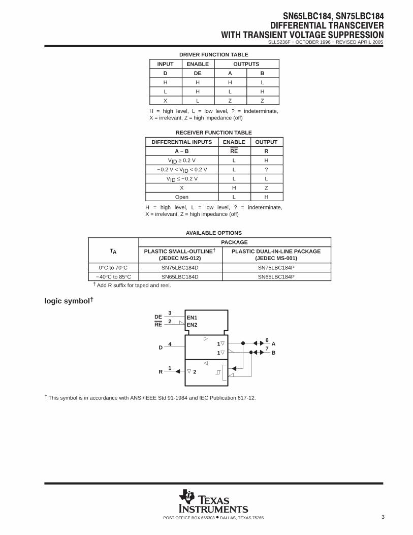
DRIVER FUNCTION TABLE
INPUT ENABLE OUTPUTS
D DE A B
H H H L
L H L H
X L Z Z
H = high level, L = low level, ? = indeterminate,X = irrelevant, Z = high impedance (off)
RECEIVER FUNCTION TABLE
DIFFERENTIAL INPUTS ENABLE OUTPUT
A − B RE R
VID ≥ 0.2 V L H
−0.2 V < VID < 0.2 V L ?
VID ≤ −0.2 V L L
X H Z
Open L H
H = high level, L = low level, ? = indeterminate,X = irrelevant, Z = high impedance (off)
AVAILABLE OPTIONS
PACKAGE
TA PLASTIC SMALL-OUTLINE †
(JEDEC MS-012)PLASTIC DUAL-IN-LINE PACKAGE
(JEDEC MS-001)
0°C to 70°C SN75LBC184D SN75LBC184P
−40°C to 85°C SN65LBC184D SN65LBC184P† Add R suffix for taped and reel.
logic symbol †
REDE
1
1
2
B
A7
6
EN2EN1
R
D
1
4
2
3
† This symbol is in accordance with ANSI/IEEE Std 91-1984 and IEC Publication 617-12.
SLLS236F − OCTOBER 1996 − REVISED APRIL 2005
4 POST OFFICE BOX 655303 • DALLAS, TEXAS 75265
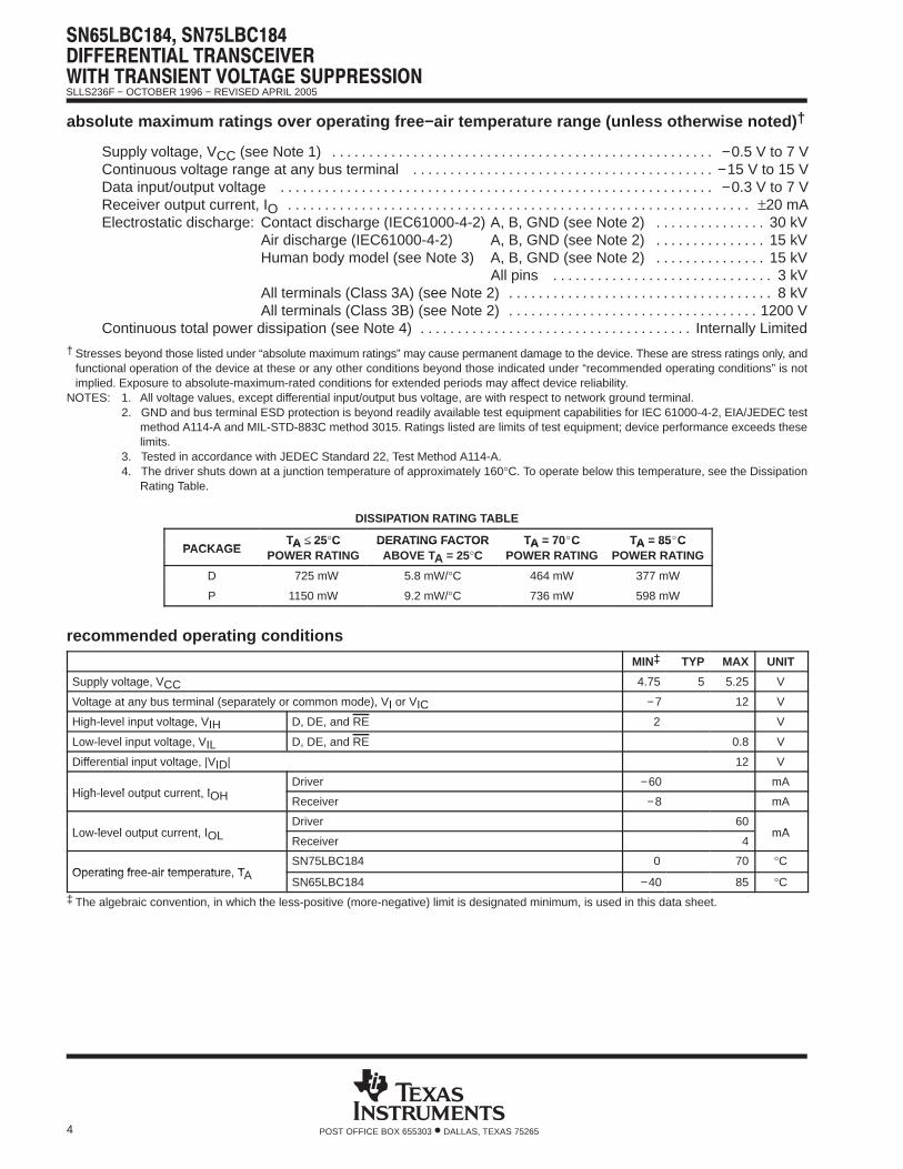
absolute maximum ratings over operating free−air temperature range (unless otherwise noted) †
Supply voltage, VCC (see Note 1) −0.5 V to 7 V. . . . . . . . . . . . . . . . . . . . . . . . . . . . . . . . . . . . . . . . . . . . . . . . . . . . Continuous voltage range at any bus terminal −15 V to 15 V. . . . . . . . . . . . . . . . . . . . . . . . . . . . . . . . . . . . . . . . . Data input/output voltage −0.3 V to 7 V. . . . . . . . . . . . . . . . . . . . . . . . . . . . . . . . . . . . . . . . . . . . . . . . . . . . . . . . . . . Receiver output current, IO ±20 mA. . . . . . . . . . . . . . . . . . . . . . . . . . . . . . . . . . . . . . . . . . . . . . . . . . . . . . . . . . . . . . . Electrostatic discharge: Contact discharge (IEC61000-4-2) A, B, GND (see Note 2) 30 kV. . . . . . . . . . . . . . .
Air discharge (IEC61000-4-2) A, B, GND (see Note 2) 15 kV. . . . . . . . . . . . . . . Human body model (see Note 3) A, B, GND (see Note 2) 15 kV. . . . . . . . . . . . . . .
All pins 3 kV. . . . . . . . . . . . . . . . . . . . . . . . . . . . . . All terminals (Class 3A) (see Note 2) 8 kV. . . . . . . . . . . . . . . . . . . . . . . . . . . . . . . . . . . . All terminals (Class 3B) (see Note 2) 1200 V. . . . . . . . . . . . . . . . . . . . . . . . . . . . . . . . . .
Continuous total power dissipation (see Note 4) Internally Limited. . . . . . . . . . . . . . . . . . . . . . . . . . . . . . . . . . . . .
† Stresses beyond those listed under “absolute maximum ratings” may cause permanent damage to the device. These are stress ratings only, andfunctional operation of the device at these or any other conditions beyond those indicated under “recommended operating conditions” is notimplied. Exposure to absolute-maximum-rated conditions for extended periods may affect device reliability.
NOTES: 1. All voltage values, except differential input/output bus voltage, are with respect to network ground terminal.2. GND and bus terminal ESD protection is beyond readily available test equipment capabilities for IEC 61000-4-2, EIA/JEDEC test
method A114-A and MIL-STD-883C method 3015. Ratings listed are limits of test equipment; device performance exceeds theselimits.
3. Tested in accordance with JEDEC Standard 22, Test Method A114-A.4. The driver shuts down at a junction temperature of approximately 160°C. To operate below this temperature, see the Dissipation
Rating Table.
DISSIPATION RATING TABLE
PACKAGETA ≤ 25°C DERATING FACTOR TA = 70C TA = 85C
PACKAGETA ≤ 25 C
POWER RATINGDERATING FACTORABOVE TA = 25°C
TA = 70 CPOWER RATING
TA = 85 CPOWER RATING
D 725 mW 5.8 mW/°C 464 mW 377 mW
P 1150 mW 9.2 mW/°C 736 mW 598 mW
recommended operating conditions
MIN‡ TYP MAX UNIT
Supply voltage, VCC 4.75 5 5.25 V
Voltage at any bus terminal (separately or common mode), VI or VIC −7 12 V
High-level input voltage, VIH D, DE, and RE 2 V
Low-level input voltage, VIL D, DE, and RE 0.8 V
Differential input voltage, |VID| 12 V
High-level output current, IOHDriver −60 mA
High-level output current, IOH Receiver −8 mA
Low-level output current, IOLDriver 60
mALow-level output current, IOL Receiver 4mA
Operating free-air temperature, TASN75LBC184 0 70 °C
Operating free-air temperature, TASN65LBC184 −40 85 °C
‡ The algebraic convention, in which the less-positive (more-negative) limit is designated minimum, is used in this data sheet.
SLLS236F − OCTOBER 1996 − REVISED APRIL 2005
5POST OFFICE BOX 655303 • DALLAS, TEXAS 75265
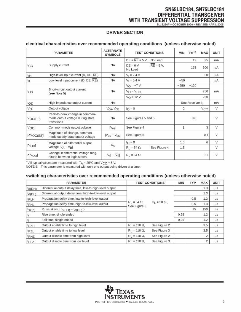
DRIVER SECTION
electrical characteristics over recommended operating conditions (unless otherwise noted)
PARAMETERALTERNATESYMBOLS TEST CONDITIONS MIN TYP† MAX UNIT
DE = RE = 5 V, No Load 12 25 mA
ICC Supply current NA DE = 0 V, RE = 5 V,No Load
175 300 µA
IIH High-level input current (D, DE, RE) NA VI = 2.4 V 50 µA
IIL Low-level input current (D, DE, RE) NA VI = 0.4 V −50 µA
Short-circuit output currentVO = −7 V −250 −120
IOSShort-circuit output current(see Note 5)
NA VO = VCC 250 mAIOS (see Note 5)NA
VO = 12 V 250
mA
IOZ High-impedance output current NA See Receiver II mA
VO Output voltage Voa, Vob IO = 0 0 VCC V
VOC(PP)
Peak-to-peak change in common-mode output voltage during statetransitions
NA See Figures 5 and 6 0.8 V
VOC Common-mode output voltage |Vos| See Figure 4 1 3 V
|∆VOC(SS)|Magnitude of change, common-mode steady-state output voltage
|Vos − Vos| See Figure 5 0.1 V
|VOD|Magnitude of differential output
VoIO = 0 1.5 6 V
|VOD|Magnitude of differential output voltage |VA − VB| Vo RL = 54 Ω, See Figure 4 1.5 V
∆|VOD|Change in differential voltage mag-nitude between logic states
||Vt| − |Vt|| RL = 54 Ω 0.1 V
† All typical values are measured with TA = 25°C and VCC = 5 V.NOTE 5: This parameter is measured with only one output being driven at a time.
switching characteristics over recommended operating conditions (unless otherwise noted)
PARAMETER TEST CONDITIONS MIN TYP MAX UNIT
td(DH) Differential output delay time, low-to-high-level output 1.3 µs
td(DL) Differential-output delay time, high-to-low-level output 1.3 µs
tPLH Propagation delay time, low-to-high-level outputRL = 54 Ω, CL = 50 pF,
0.5 1.3 µs
tPHL Propagation delay time, high-to-low-level outputRL = 54 Ω,See Figure 5
CL = 50 pF,0.5 1.3 µs
tsk(p) Pulse skew (| td(DH) − td(DL) |)See Figure 5
75 150 ns
tr Rise time, single ended 0.25 1.2 µs
tf Fall time, single ended 0.25 1.2 µs
tPZH Output enable time to high level RL = 110 Ω, See Figure 2 3.5 µs
tPZL Output enable time to low level RL = 110 Ω, See Figure 3 3.5 µs
tPHZ Output disable time from high level RL = 110 Ω, See Figure 2 2 µs
tPLZ Output disable time from low level RL = 110 Ω, See Figure 3 2 µs
SLLS236F − OCTOBER 1996 − REVISED APRIL 2005
6 POST OFFICE BOX 655303 • DALLAS, TEXAS 75265
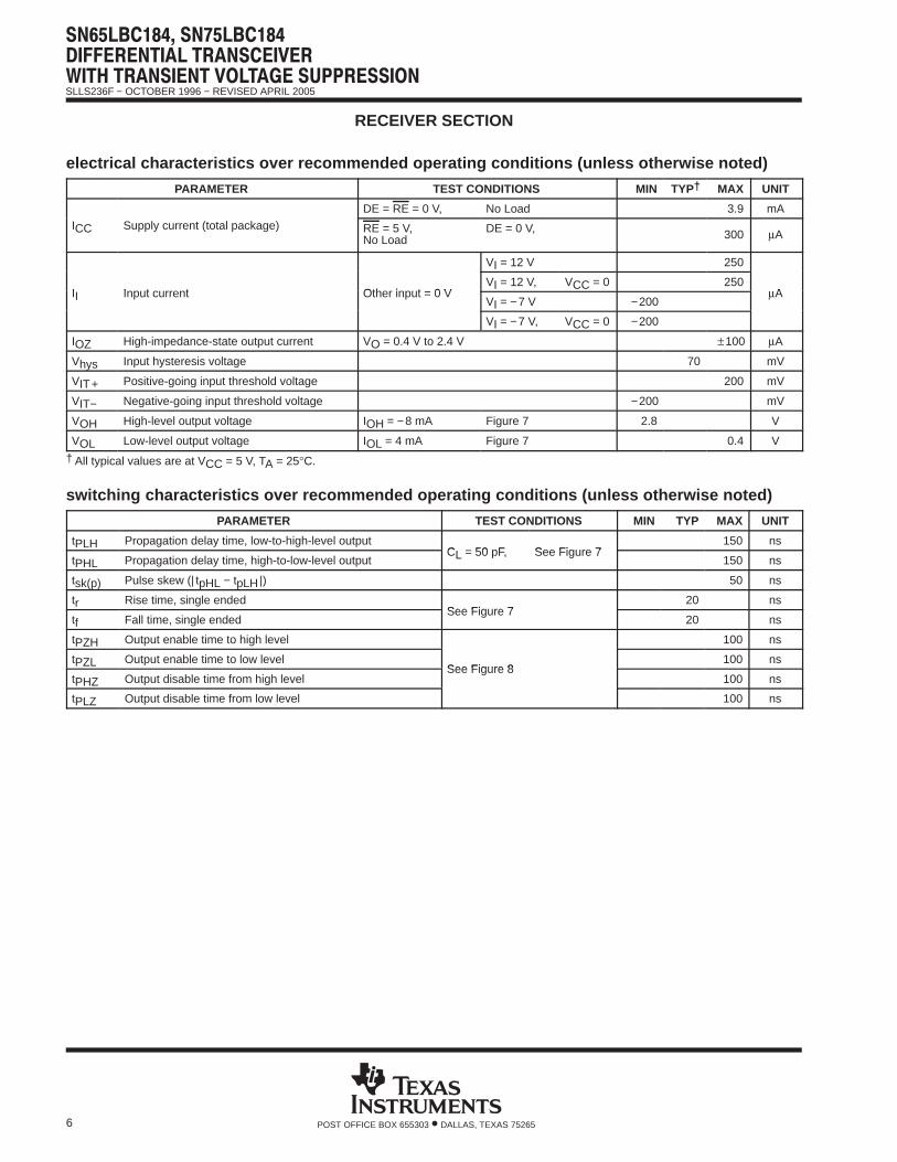
RECEIVER SECTION
electrical characteristics over recommended operating conditions (unless otherwise noted)
PARAMETER TEST CONDITIONS MIN TYP† MAX UNIT
DE = RE = 0 V, No Load 3.9 mAICC Supply current (total package) RE = 5 V,
No LoadDE = 0 V, 300 µA
VI = 12 V 250
II Input current Other input = 0 VVI = 12 V, VCC = 0 250
AII Input current Other input = 0 VVI = −7 V −200
µA
VI = −7 V, VCC = 0 −200
IOZ High-impedance-state output current VO = 0.4 V to 2.4 V ±100 µA
Vhys Input hysteresis voltage 70 mV
VIT+ Positive-going input threshold voltage 200 mV
VIT− Negative-going input threshold voltage −200 mV
VOH High-level output voltage IOH = −8 mA Figure 7 2.8 V
VOL Low-level output voltage IOL = 4 mA Figure 7 0.4 V
† All typical values are at VCC = 5 V, TA = 25°C.
switching characteristics over recommended operating conditions (unless otherwise noted)
PARAMETER TEST CONDITIONS MIN TYP MAX UNIT
tPLH Propagation delay time, low-to-high-level outputCL = 50 pF, See Figure 7
150 ns
tPHL Propagation delay time, high-to-low-level outputCL = 50 pF, See Figure 7
150 ns
tsk(p) Pulse skew (| tpHL − tpLH|) 50 ns
tr Rise time, single endedSee Figure 7
20 ns
tf Fall time, single endedSee Figure 7
20 ns
tPZH Output enable time to high level 100 ns
tPZL Output enable time to low levelSee Figure 8
100 ns
tPHZ Output disable time from high levelSee Figure 8
100 ns
tPLZ Output disable time from low level 100 ns
SLLS236F − OCTOBER 1996 − REVISED APRIL 2005
7POST OFFICE BOX 655303 • DALLAS, TEXAS 75265
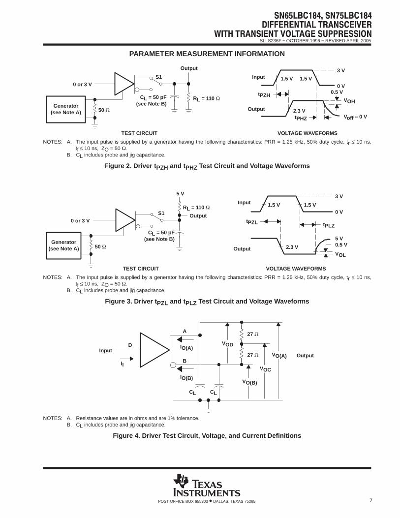
PARAMETER MEASUREMENT INFORMATION
VOLTAGE WAVEFORMS
tPHZ
1.5 V
2.3 V
0.5 V0 V
3 V
tPZH
Output
Input 1.5 VS10 or 3 V
Output
CL = 50 pF(see Note B)
TEST CIRCUIT
50 Ω
VOH
Voff ≈ 0 V
RL = 110 ΩGenerator
(see Note A)
NOTES: A. The input pulse is supplied by a generator having the following characteristics: PRR = 1.25 kHz, 50% duty cycle, tr ≤ 10 ns,tf ≤ 10 ns, ZO = 50 Ω.
B. CL includes probe and jig capacitance.
Figure 2. Driver t PZH and t PHZ Test Circuit and Voltage Waveforms
VOLTAGE WAVEFORMS
5 V
VOL
0.5 V
tPZL
3 V
0 V
tPLZ
2.3 V
1.5 V
Output
Input
TEST CIRCUIT
Output
RL = 110 Ω
5 V
S1
CL = 50 pF(see Note B)
50 Ω
0 or 3 V
Generator(see Note A)
1.5 V
NOTES: A. The input pulse is supplied by a generator having the following characteristics: PRR = 1.25 kHz, 50% duty cycle, tr ≤ 10 ns,tf ≤ 10 ns, ZO = 50 Ω.
B. CL includes probe and jig capacitance.
Figure 3. Driver t PZL and t PLZ Test Circuit and Voltage Waveforms
IO(A)
A
B
IO(B)
CL CL
VOD
VO(B)
VOC
27 Ω
27 Ω VO(A)
D
II
InputOutput
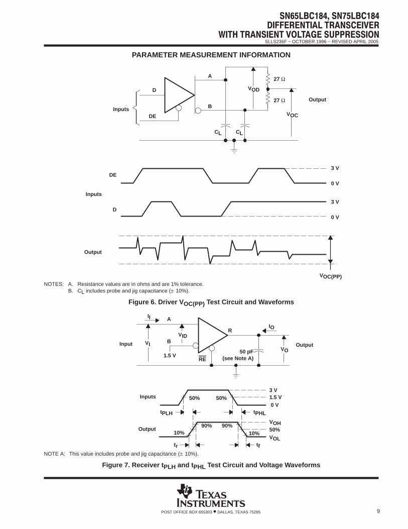
NOTES: A. Resistance values are in ohms and are 1% tolerance.B. CL includes probe and jig capacitance.
Figure 4. Driver Test Circuit, Voltage, and Current Definitions
SLLS236F − OCTOBER 1996 − REVISED APRIL 2005
8 POST OFFICE BOX 655303 • DALLAS, TEXAS 75265
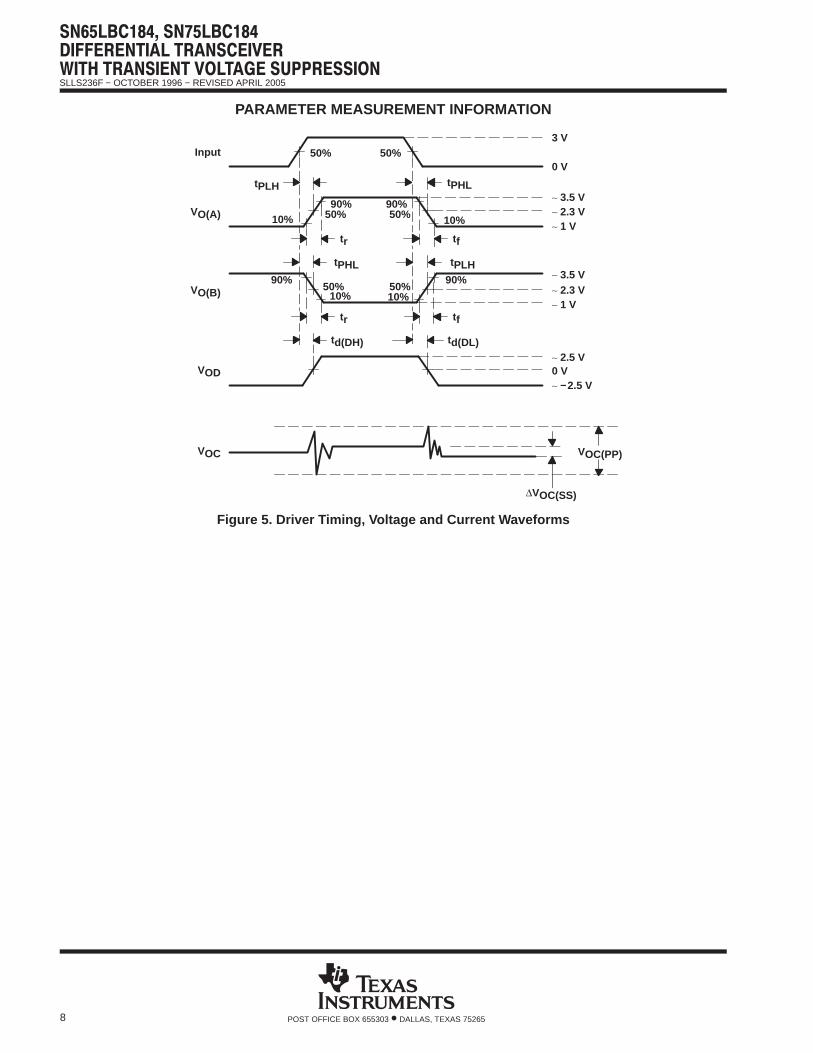
PARAMETER MEASUREMENT INFORMATION
50% 50%
90% 90%50% 50%10% 10%
90%90%50% 50%
10%10%
3 V
0 V
∼ 3.5 V∼ 2.3 V∼ 1 V
∼ 3.5 V∼ 2.3 V∼ 1 V
∼ 2.5 V0 V∼ −2.5 V
Input
VO(A)
VO(B)
VOD
tPLH tPHL
tr tf
tPHL tPLH
tr tf
td(DH) td(DL)
VOC(PP)
∆VOC(SS)
VOC
Figure 5. Driver Timing, Voltage and Current Waveforms
SLLS236F − OCTOBER 1996 − REVISED APRIL 2005
9POST OFFICE BOX 655303 • DALLAS, TEXAS 75265
PARAMETER MEASUREMENT INFORMATION
A
B
CL CL
VOD
VOC
27 Ω
27 Ω
D
Inputs
Output
DE
3 V
0 V
3 V
0 V
DE
D
Inputs
VOC(PP)
Output
NOTES: A. Resistance values are in ohms and are 1% tolerance.B. CL includes probe and jig capacitance (± 10%).
Figure 6. Driver V OC(PP) Test Circuit and Waveforms
R
50 pF(see Note A)
VO
A
Input Output
3 V
0 V
Inputs
Output
IOVID
1.5 V
B
RE
VI
II
tPLH tPHL
tr tf
1.5 V
VOH
VOL
50%90%
10%
50%
90%10%
50%
NOTE A: This value includes probe and jig capacitance (± 10%).
Figure 7. Receiver t PLH and t PHL Test Circuit and Voltage Waveforms
SLLS236F − OCTOBER 1996 − REVISED APRIL 2005
10 POST OFFICE BOX 655303 • DALLAS, TEXAS 75265
PARAMETER MEASUREMENT INFORMATION
3 V
0 V
Inputs
Output
tPHZ tPZH
VOH
∼ 2.5 V
0.5 V
R
50 pF(see Note A)
VO
A
Input
B
RE
620 Ω
620 Ω
5 V
0 V or 3 V
1.5 V
0.5 V
RE
VO
3 V
0 VtPLZ tPZL
VOL
∼ 2.5 V
0.5 V
1.5 V
0.5 V
3 V
0 VA
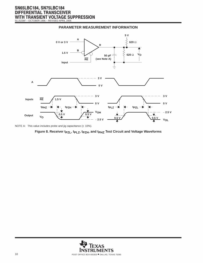
NOTE A: This value includes probe and jig capacitance (± 10%).
Figure 8. Receiver t PZL, tPLZ, tPZH, and t PHZ Test Circuit and Voltage Waveforms
SLLS236F − OCTOBER 1996 − REVISED APRIL 2005
11POST OFFICE BOX 655303 • DALLAS, TEXAS 75265
TYPICAL CHARACTERISTICS
1.0
1.5
2.0
2.5
3.0
−40 −20 0 20 40 60 80
Figure 9
TA − Free-Air Temperature − °C
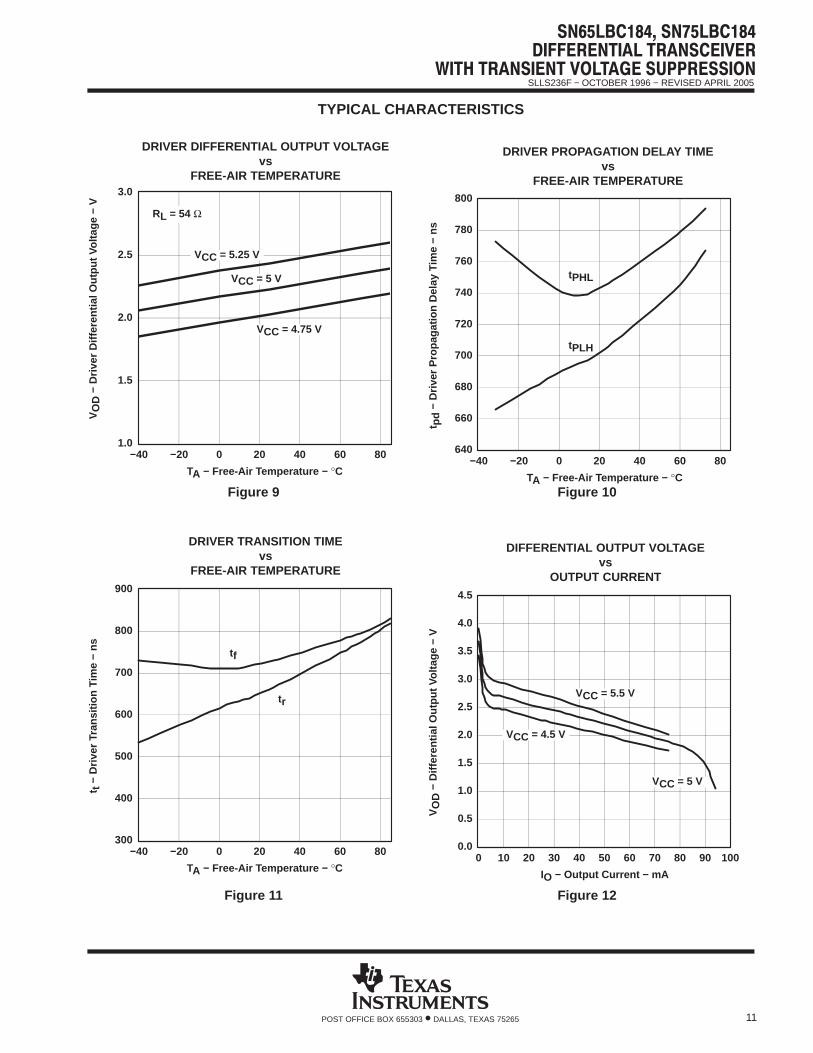
RL = 54 Ω
VO
D −
Driv
er D
iffer
entia
l Out
put V
olta
ge −
V
DRIVER DIFFERENTIAL OUTPUT VOLTAGEvs
FREE-AIR TEMPERATURE
VCC = 4.75 V
VCC = 5 V
VCC = 5.25 V
TA − Free-Air Temperature − °C
640
660
680
700
720
740
760
780
800
−40 −20 0 20 40 60 80
t pd
− D
river
Pro
paga
tion
Del
ay T
ime
− ns
DRIVER PROPAGATION DELAY TIMEvs
FREE-AIR TEMPERATURE
tPLH
tPHL
Figure 10
300
400
500
600
700
800
900
−40 −20 0 20 40 60 80
Figure 11
TA − Free-Air Temperature − °C
t t −
Driv
er T
rans
ition
Ti
me
− ns
DRIVER TRANSITION TIMEvs
FREE-AIR TEMPERATURE
tf
tr
IO − Output Current − mA
0.0
0.5
1.0
1.5
2.0
2.5
3.0
3.5
4.0
4.5
0 10 20 30 40 50 60 70 80 90 100
VO
D −
Diff
eren
tial O
utpu
t Vol
tage
− V
DIFFERENTIAL OUTPUT VOLTAGEvs
OUTPUT CURRENT
VCC = 5.5 V
VCC = 5 V
VCC = 4.5 V
Figure 12
SLLS236F − OCTOBER 1996 − REVISED APRIL 2005
12 POST OFFICE BOX 655303 • DALLAS, TEXAS 75265
TYPICAL CHARACTERISTICS
VI − Input Voltage − V
−0.20
−0.15
−0.10
−0.05
−0.00
0.05
0.10
0.15
0.20
0.25
−10 −5 0 5 10 15
I (I)
− R
ecei
ver
Inpu
t Cur
rent
− m
A
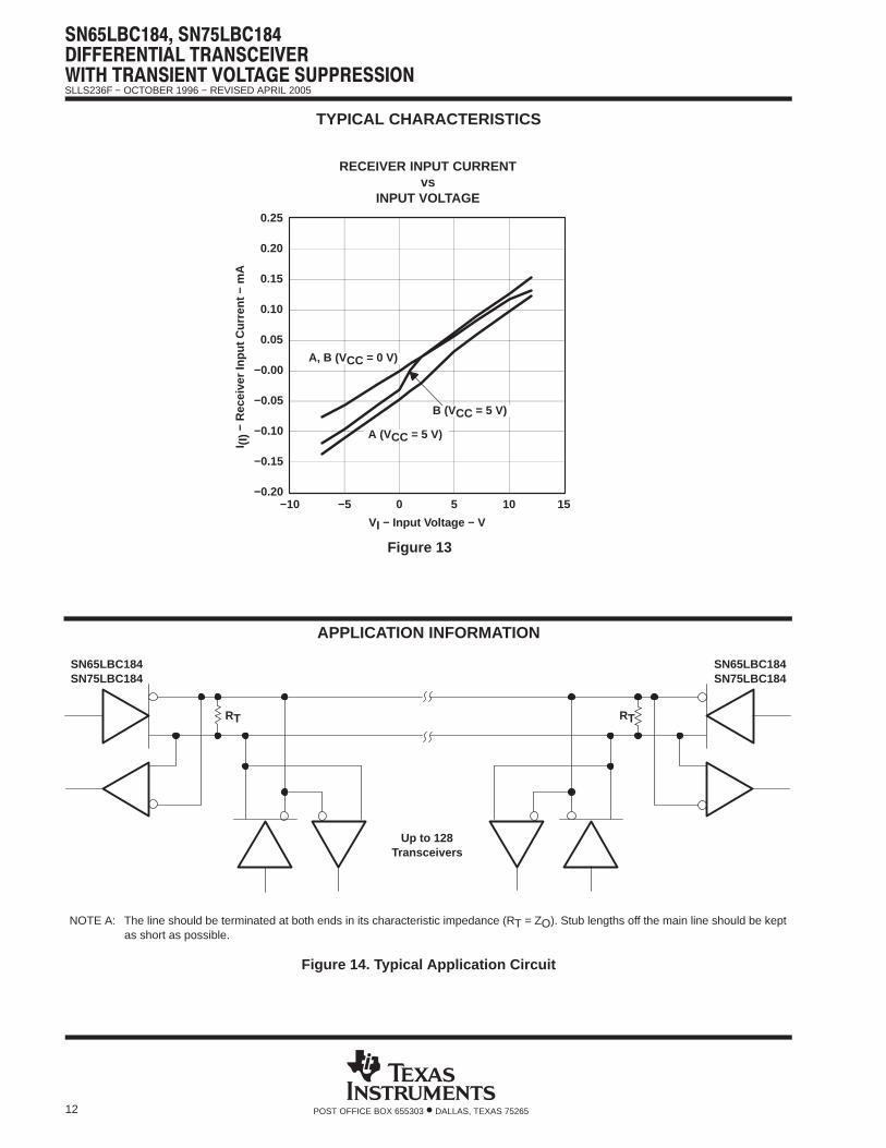
RECEIVER INPUT CURRENTvs
INPUT VOLTAGE
A, B (VCC = 0 V)
A (VCC = 5 V)
B (VCC = 5 V)
Figure 13
APPLICATION INFORMATION
Up to 128Transceivers
SN65LBC184SN75LBC184
SN65LBC184SN75LBC184
RT RT
NOTE A: The line should be terminated at both ends in its characteristic impedance (RT = ZO). Stub lengths off the main line should be keptas short as possible.
Figure 14. Typical Application Circuit
SLLS236F − OCTOBER 1996 − REVISED APRIL 2005
13POST OFFICE BOX 655303 • DALLAS, TEXAS 75265
APPLICATION INFORMATION
’LBC184 test description
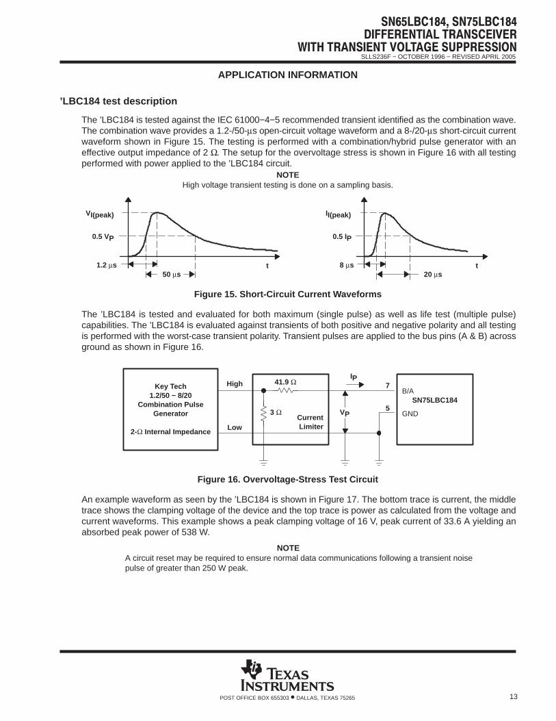
The ’LBC184 is tested against the IEC 61000−4−5 recommended transient identified as the combination wave.The combination wave provides a 1.2-/50-µs open-circuit voltage waveform and a 8-/20-µs short-circuit currentwaveform shown in Figure 15. The testing is performed with a combination/hybrid pulse generator with aneffective output impedance of 2 Ω. The setup for the overvoltage stress is shown in Figure 16 with all testingperformed with power applied to the ’LBC184 circuit.
NOTEHigh voltage transient testing is done on a sampling basis.
VI(peak) II(peak)
0.5 VP 0.5 IP
1.2 µs50 µs 20 µs
8 µst t
Figure 15. Short-Circuit Current Waveforms
The ’LBC184 is tested and evaluated for both maximum (single pulse) as well as life test (multiple pulse)capabilities. The ’LBC184 is evaluated against transients of both positive and negative polarity and all testingis performed with the worst-case transient polarity. Transient pulses are applied to the bus pins (A & B) acrossground as shown in Figure 16.
SN75LBC184
Key Tech1.2/50 − 8/20
Combination PulseGenerator
2-Ω Internal Impedance
7
5
IP41.9 Ω
3 ΩCurrentLimiter
VP
High
Low
GND
B/A
Figure 16. Overvoltage-Stress Test Circuit
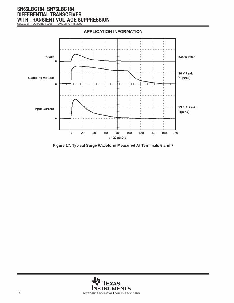
An example waveform as seen by the ’LBC184 is shown in Figure 17. The bottom trace is current, the middletrace shows the clamping voltage of the device and the top trace is power as calculated from the voltage andcurrent waveforms. This example shows a peak clamping voltage of 16 V, peak current of 33.6 A yielding anabsorbed peak power of 538 W.
NOTEA circuit reset may be required to ensure normal data communications following a transient noisepulse of greater than 250 W peak.
SLLS236F − OCTOBER 1996 − REVISED APRIL 2005
14 POST OFFICE BOX 655303 • DALLAS, TEXAS 75265
APPLICATION INFORMATION
Power
Clamping Voltage
Input Current
0 20 40 60
t − 20 µs/Div
538 W Peak
16 V Peak,VI(peak)
33.6 A Peak,II(peak)
0
0
0
80 100 120 140 160 180
Figure 17. Typical Surge Waveform Measured At Terminals 5 and 7
SLLS236F − OCTOBER 1996 − REVISED APRIL 2005
15POST OFFICE BOX 655303 • DALLAS, TEXAS 75265
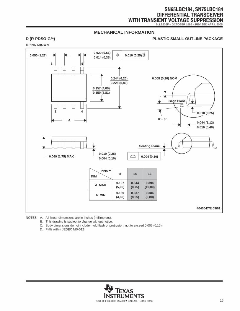
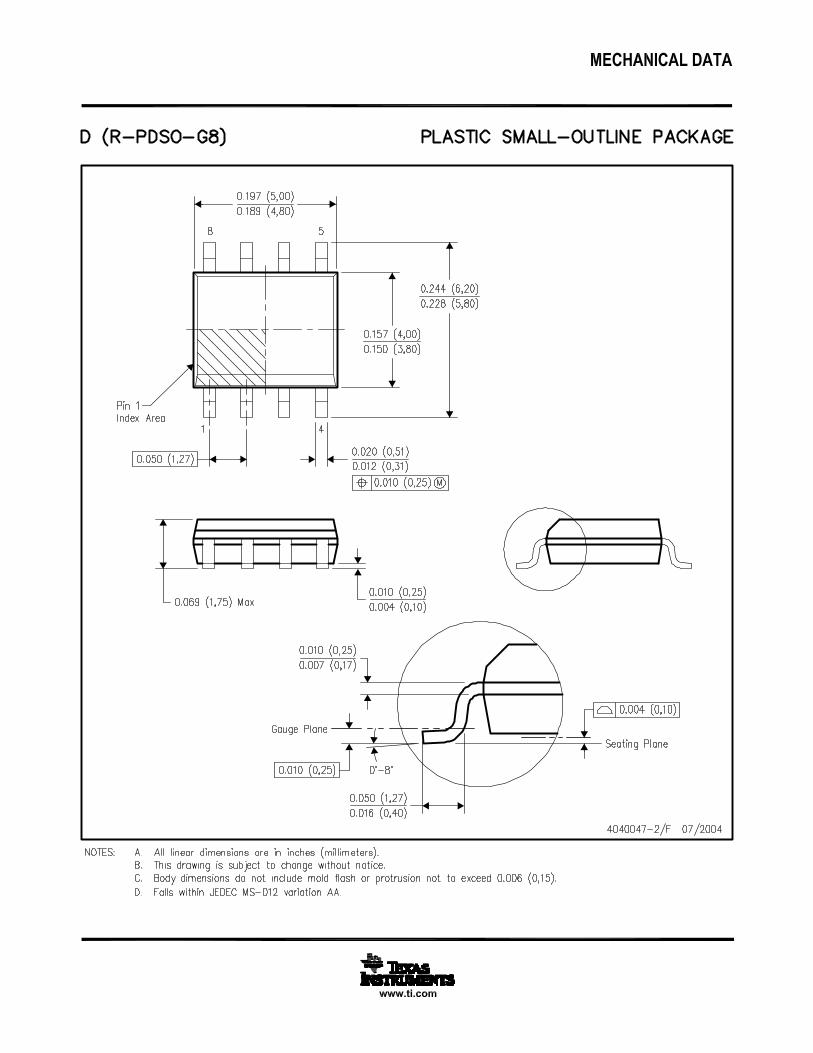
MECHANICAL INFORMATIOND (R-PDSO-G**) PLASTIC SMALL-OUTLINE PACKAGE8 PINS SHOWN
8
0.197(5,00)
A MAX
A MIN(4,80)0.189 0.337
(8,55)
(8,75)0.344
14
0.386(9,80)
(10,00)0.394
16DIM
PINS **
4040047/E 09/01
0.069 (1,75) MAX
Seating Plane
0.004 (0,10)0.010 (0,25)
0.010 (0,25)
0.016 (0,40)0.044 (1,12)
0.244 (6,20)0.228 (5,80)
0.020 (0,51)0.014 (0,35)
1 4
8 5
0.150 (3,81)0.157 (4,00)
0.008 (0,20) NOM
0°− 8°
Gage Plane
A
0.004 (0,10)
0.010 (0,25)0.050 (1,27)
NOTES: A. All linear dimensions are in inches (millimeters).B. This drawing is subject to change without notice.C. Body dimensions do not include mold flash or protrusion, not to exceed 0.006 (0,15).D. Falls within JEDEC MS-012
SLLS236F − OCTOBER 1996 − REVISED APRIL 2005
16 POST OFFICE BOX 655303 • DALLAS, TEXAS 75265
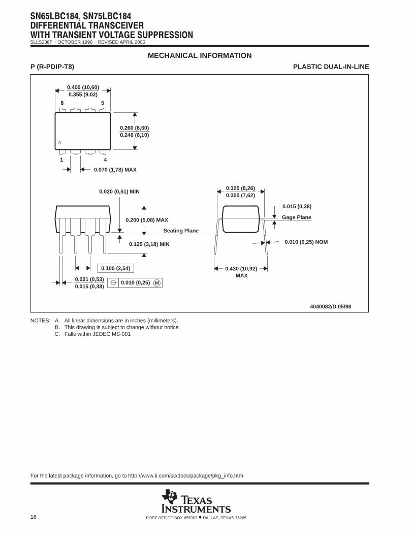
MECHANICAL INFORMATIONP (R-PDIP-T8) PLASTIC DUAL-IN-LINE
8
4
0.015 (0,38)
Gage Plane
0.325 (8,26)0.300 (7,62)
0.010 (0,25) NOM
MAX0.430 (10,92)
4040082/D 05/98
0.200 (5,08) MAX
0.125 (3,18) MIN
5
0.355 (9,02)
0.020 (0,51) MIN
0.070 (1,78) MAX
0.240 (6,10)0.260 (6,60)
0.400 (10,60)
1
0.015 (0,38)0.021 (0,53)
Seating Plane
M0.010 (0,25)
0.100 (2,54)
NOTES: A. All linear dimensions are in inches (millimeters).B. This drawing is subject to change without notice.C. Falls within JEDEC MS-001
For the latest package information, go to http://www.ti.com/sc/docs/package/pkg_info.htm
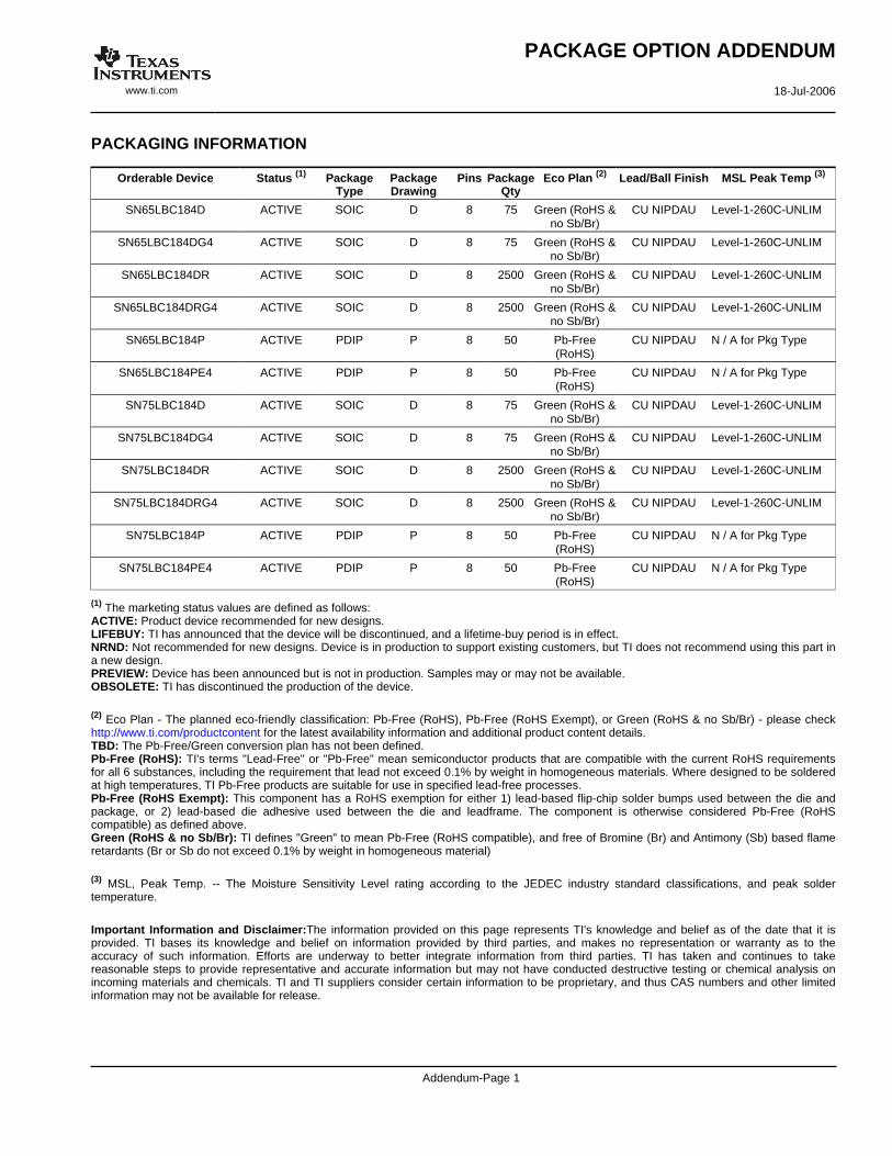
PACKAGING INFORMATION
Orderable Device Status (1) PackageType
PackageDrawing
Pins PackageQty
Eco Plan (2) Lead/Ball Finish MSL Peak Temp (3)
SN65LBC184D ACTIVE SOIC D 8 75 Green (RoHS &no Sb/Br)
CU NIPDAU Level-1-260C-UNLIM
SN65LBC184DG4 ACTIVE SOIC D 8 75 Green (RoHS &no Sb/Br)
CU NIPDAU Level-1-260C-UNLIM
SN65LBC184DR ACTIVE SOIC D 8 2500 Green (RoHS &no Sb/Br)
CU NIPDAU Level-1-260C-UNLIM
SN65LBC184DRG4 ACTIVE SOIC D 8 2500 Green (RoHS &no Sb/Br)
CU NIPDAU Level-1-260C-UNLIM
SN65LBC184P ACTIVE PDIP P 8 50 Pb-Free(RoHS)
CU NIPDAU N / A for Pkg Type
SN65LBC184PE4 ACTIVE PDIP P 8 50 Pb-Free(RoHS)
CU NIPDAU N / A for Pkg Type
SN75LBC184D ACTIVE SOIC D 8 75 Green (RoHS &no Sb/Br)
CU NIPDAU Level-1-260C-UNLIM
SN75LBC184DG4 ACTIVE SOIC D 8 75 Green (RoHS &no Sb/Br)
CU NIPDAU Level-1-260C-UNLIM
SN75LBC184DR ACTIVE SOIC D 8 2500 Green (RoHS &no Sb/Br)
CU NIPDAU Level-1-260C-UNLIM
SN75LBC184DRG4 ACTIVE SOIC D 8 2500 Green (RoHS &no Sb/Br)
CU NIPDAU Level-1-260C-UNLIM
SN75LBC184P ACTIVE PDIP P 8 50 Pb-Free(RoHS)
CU NIPDAU N / A for Pkg Type
SN75LBC184PE4 ACTIVE PDIP P 8 50 Pb-Free(RoHS)
CU NIPDAU N / A for Pkg Type
(1) The marketing status values are defined as follows:ACTIVE: Product device recommended for new designs.LIFEBUY: TI has announced that the device will be discontinued, and a lifetime-buy period is in effect.NRND: Not recommended for new designs. Device is in production to support existing customers, but TI does not recommend using this part ina new design.PREVIEW: Device has been announced but is not in production. Samples may or may not be available.OBSOLETE: TI has discontinued the production of the device.
(2) Eco Plan - The planned eco-friendly classification: Pb-Free (RoHS), Pb-Free (RoHS Exempt), or Green (RoHS & no Sb/Br) - please checkhttp://www.ti.com/productcontent for the latest availability information and additional product content details.TBD: The Pb-Free/Green conversion plan has not been defined.Pb-Free (RoHS): TI's terms "Lead-Free" or "Pb-Free" mean semiconductor products that are compatible with the current RoHS requirementsfor all 6 substances, including the requirement that lead not exceed 0.1% by weight in homogeneous materials. Where designed to be solderedat high temperatures, TI Pb-Free products are suitable for use in specified lead-free processes.Pb-Free (RoHS Exempt): This component has a RoHS exemption for either 1) lead-based flip-chip solder bumps used between the die andpackage, or 2) lead-based die adhesive used between the die and leadframe. The component is otherwise considered Pb-Free (RoHScompatible) as defined above.Green (RoHS & no Sb/Br): TI defines "Green" to mean Pb-Free (RoHS compatible), and free of Bromine (Br) and Antimony (Sb) based flameretardants (Br or Sb do not exceed 0.1% by weight in homogeneous material)
(3) MSL, Peak Temp. -- The Moisture Sensitivity Level rating according to the JEDEC industry standard classifications, and peak soldertemperature.
Important Information and Disclaimer:The information provided on this page represents TI's knowledge and belief as of the date that it isprovided. TI bases its knowledge and belief on information provided by third parties, and makes no representation or warranty as to theaccuracy of such information. Efforts are underway to better integrate information from third parties. TI has taken and continues to takereasonable steps to provide representative and accurate information but may not have conducted destructive testing or chemical analysis onincoming materials and chemicals. TI and TI suppliers consider certain information to be proprietary, and thus CAS numbers and other limitedinformation may not be available for release.
PACKAGE OPTION ADDENDUM
www.ti.com 18-Jul-2006
Addendum-Page 1
In no event shall TI's liability arising out of such information exceed the total purchase price of the TI part(s) at issue in this document sold by TIto Customer on an annual basis.
PACKAGE OPTION ADDENDUM
www.ti.com 18-Jul-2006
Addendum-Page 2
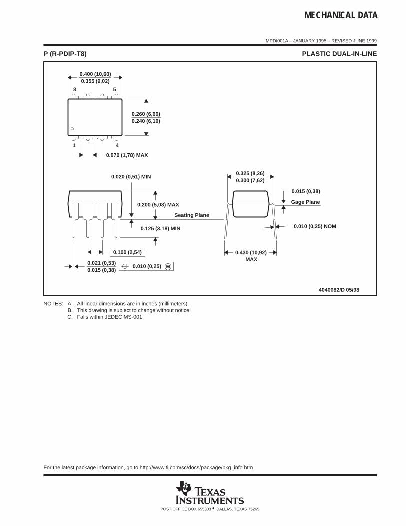
MECHANICAL DATA
MPDI001A – JANUARY 1995 – REVISED JUNE 1999
POST OFFICE BOX 655303 • DALLAS, TEXAS 75265
P (R-PDIP-T8) PLASTIC DUAL-IN-LINE
8
4
0.015 (0,38)
Gage Plane
0.325 (8,26)0.300 (7,62)
0.010 (0,25) NOM
MAX0.430 (10,92)
4040082/D 05/98
0.200 (5,08) MAX
0.125 (3,18) MIN
5
0.355 (9,02)
0.020 (0,51) MIN
0.070 (1,78) MAX
0.240 (6,10)0.260 (6,60)
0.400 (10,60)
1
0.015 (0,38)0.021 (0,53)
Seating Plane
M0.010 (0,25)
0.100 (2,54)
NOTES: A. All linear dimensions are in inches (millimeters).B. This drawing is subject to change without notice.C. Falls within JEDEC MS-001
For the latest package information, go to http://www.ti.com/sc/docs/package/pkg_info.htm
IMPORTANT NOTICE
Texas Instruments Incorporated and its subsidiaries (TI) reserve the right to make corrections, modifications,enhancements, improvements, and other changes to its products and services at any time and to discontinueany product or service without notice. Customers should obtain the latest relevant information before placingorders and should verify that such information is current and complete. All products are sold subject to TI’s termsand conditions of sale supplied at the time of order acknowledgment.
TI warrants performance of its hardware products to the specifications applicable at the time of sale inaccordance with TI’s standard warranty. Testing and other quality control techniques are used to the extent TIdeems necessary to support this warranty. Except where mandated by government requirements, testing of allparameters of each product is not necessarily performed.
TI assumes no liability for applications assistance or customer product design. Customers are responsible fortheir products and applications using TI components. To minimize the risks associated with customer productsand applications, customers should provide adequate design and operating safeguards.
TI does not warrant or represent that any license, either express or implied, is granted under any TI patent right,copyright, mask work right, or other TI intellectual property right relating to any combination, machine, or processin which TI products or services are used. Information published by TI regarding third-party products or servicesdoes not constitute a license from TI to use such products or services or a warranty or endorsement thereof.Use of such information may require a license from a third party under the patents or other intellectual propertyof the third party, or a license from TI under the patents or other intellectual property of TI.
Reproduction of information in TI data books or data sheets is permissible only if reproduction is withoutalteration and is accompanied by all associated warranties, conditions, limitations, and notices. Reproductionof this information with alteration is an unfair and deceptive business practice. TI is not responsible or liable forsuch altered documentation.
Resale of TI products or services with statements different from or beyond the parameters stated by TI for thatproduct or service voids all express and any implied warranties for the associated TI product or service andis an unfair and deceptive business practice. TI is not responsible or liable for any such statements.
Following are URLs where you can obtain information on other Texas Instruments products and applicationsolutions:
Products Applications
Amplifiers amplifier.ti.com Audio www.ti.com/audio
Data Converters dataconverter.ti.com Automotive www.ti.com/automotive
DSP dsp.ti.com Broadband www.ti.com/broadband
Interface interface.ti.com Digital Control www.ti.com/digitalcontrol
Logic logic.ti.com Military www.ti.com/military
Power Mgmt power.ti.com Optical Networking www.ti.com/opticalnetwork
Microcontrollers microcontroller.ti.com Security www.ti.com/security
Low Power Wireless www.ti.com/lpw Telephony www.ti.com/telephony
Video & Imaging www.ti.com/video
Wireless www.ti.com/wireless
Mailing Address: Texas Instruments
Post Office Box 655303 Dallas, Texas 75265
Copyright 2006, Texas Instruments Incorporated


