Embed Size (px)
Citation preview
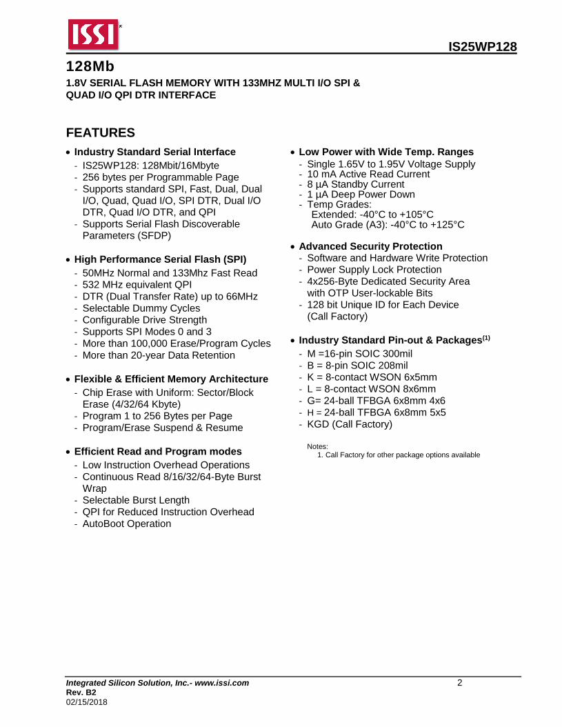
IS25WP128
128Mb 1.8V SERIAL FLASH MEMORY WITH 133MHZ MULTI I/O SPI &
QUAD I/O QPI DTR INTERFACE
DATA SHEET
IS25WP128
Integrated Silicon Solution, Inc.- www.issi.com 2 Rev. B2
02/15/2018
FEATURES
Industry Standard Serial Interface
- IS25WP128: 128Mbit/16Mbyte - 256 bytes per Programmable Page - Supports standard SPI, Fast, Dual, Dual
I/O, Quad, Quad I/O, SPI DTR, Dual I/O DTR, Quad I/O DTR, and QPI
- Supports Serial Flash Discoverable Parameters (SFDP)
High Performance Serial Flash (SPI)
- 50MHz Normal and 133Mhz Fast Read - 532 MHz equivalent QPI - DTR (Dual Transfer Rate) up to 66MHz - Selectable Dummy Cycles - Configurable Drive Strength - Supports SPI Modes 0 and 3 - More than 100,000 Erase/Program Cycles - More than 20-year Data Retention
Flexible & Efficient Memory Architecture
- Chip Erase with Uniform: Sector/Block Erase (4/32/64 Kbyte)
- Program 1 to 256 Bytes per Page - Program/Erase Suspend & Resume
Efficient Read and Program modes
- Low Instruction Overhead Operations - Continuous Read 8/16/32/64-Byte Burst
Wrap - Selectable Burst Length - QPI for Reduced Instruction Overhead - AutoBoot Operation
Low Power with Wide Temp. Ranges
- Single 1.65V to 1.95V Voltage Supply - 10 mA Active Read Current - 8 µA Standby Current - 1 µA Deep Power Down - Temp Grades:
Extended: -40°C to +105°C Auto Grade (A3): -40°C to +125°C
Advanced Security Protection
- Software and Hardware Write Protection - Power Supply Lock Protection - 4x256-Byte Dedicated Security Area
with OTP User-lockable Bits - 128 bit Unique ID for Each Device
(Call Factory)
Industry Standard Pin-out & Packages(1)
- M =16-pin SOIC 300mil - B = 8-pin SOIC 208mil - K = 8-contact WSON 6x5mm - L = 8-contact WSON 8x6mm - G= 24-ball TFBGA 6x8mm 4x6 - H = 24-ball TFBGA 6x8mm 5x5 - KGD (Call Factory)
Notes: 1. Call Factory for other package options available
128Mb 1.8V SERIAL FLASH MEMORY WITH 133MHZ MULTI I/O SPI &
QUAD I/O QPI DTR INTERFACE
IS25WP128
Integrated Silicon Solution, Inc.- www.issi.com 3 Rev. B2
02/15/2018
GENERAL DESCRIPTION The IS25WP128 Serial Flash memory offers a versatile storage solution with high flexibility and performance in a simplified pin count package. ISSI’s “Industry Standard Serial Interface” Flash is for systems that require limited space, a low pin count, and low power consumption. The device is accessed through a 4-wire SPI Interface consisting of a Serial Data Input (SI), Serial Data Output (SO), Serial Clock (SCK), and Chip Enable (CE#) pins, which can also be configured to serve as multi-I/O (see pin descriptions). The device supports Dual and Quad I/O as well as standard, Dual Output, and Quad Output SPI. Clock frequencies of up to 133MHz allow for equivalent clock rates of up to 532MHz (133MHz x 4) which equates to 66Mbytes/s of data throughput. The IS25xP series of Flash adds support for DTR (Double Transfer Rate) commands that transfer addresses and read data on both edges of the clock. These transfer rates can outperform 16-bit Parallel Flash memories allowing for efficient memory access to support XIP (execute in place) operation. The memory array is organized into programmable pages of 256-bytes. This family supports page program mode where 1 to 256 bytes of data are programmed in a single command. QPI (Quad Peripheral Interface) supports 2-cycle instruction further reducing instruction times. Pages can be erased in groups of 4Kbyte sectors, 32Kbyte blocks, 64Kbyte blocks, and/or the entire chip. The uniform sector and block architecture allows for a high degree of flexibility so that the device can be utilized for a broad variety of applications requiring solid data retention.
GLOSSARY Standard SPI In this operation, a 4-wire SPI Interface is utilized, consisting of Serial Data Input (SI), Serial Data Output (SO), Serial Clock (SCK), and Chip Enable (CE#) pins. Instructions are sent via the SI pin to encode instructions, addresses, or input data to the device on the rising edge of SCK. The SO pin is used to read data or to check the status of the device. This device supports SPI bus operation modes (0,0) and (1,1). Mutil I/O SPI Multi-I/O operation utilizes an enhanced SPI protocol to allow the device to function with Dual Output, Dual Input and Output, Quad Output, and Quad Input and Output capability. Executing these instructions through SPI mode will achieve double or quadruple the transfer bandwidth for READ and PROGRAM operations. QPI The device supports Quad Peripheral Interface (QPI) operations only when the device is switched from Standard/Dual/Quad SPI mode to QPI mode using the enter QPI (35h) instruction. The typical SPI protocol requires that the byte-long instruction code being shifted into the device only via SI pin in eight serial clocks. The QPI mode utilizes all four I/O pins to input the instruction code thus requiring only two serial clocks. This can significantly reduce the SPI instruction overhead and improve system performance. Only QPI mode or SPI/Dual/Quad mode can be active at any given time. Enter QPI (35h) and Exit QPI (F5h) instructions are used to switch between these two modes, regardless of the non-volatile Quad Enable (QE) bit status in the Status Register. Power Reset or Hardware/Software Reset will return the device into the standard SPI mode. SI and SO pins become bidirectional I/O0 and I/O1, and WP# and HOLD# pins become I/O2 and I/O3 respectively during QPI mode. DTR In addition to SPI and QPI features, the device also supports Fast READ DTR operation. DTR operation allows high data throughput while running at lower clock frequencies. Fast READ DTR operation uses both rising and falling edges of the clock for address inputs, and data outputs, resulting in reducing input and output cycles by half.
IS25WP128
Integrated Silicon Solution, Inc.- www.issi.com 4 Rev. B2
02/15/2018
TABLE OF CONTENTS
FEATURES ............................................................................................................................................................ 2
GENERAL DESCRIPTION .................................................................................................................................... 3
TABLE OF CONTENTS ......................................................................................................................................... 4
1. PIN CONFIGURATION ................................................................................................................................... 7
2. PIN DESCRIPTIONS ...................................................................................................................................... 9
3. BLOCK DIAGRAM ........................................................................................................................................ 11
4. SPI MODES DESCRIPTION ........................................................................................................................ 12
5. SYSTEM CONFIGURATION ........................................................................................................................ 14
5.1 BLOCK/SECTOR ADDRESSES ............................................................................................................ 14
6. REGISTERS ................................................................................................................................................. 15
6.1 STATUS REGISTER .............................................................................................................................. 15
6.2 FUNCTION REGISTER .......................................................................................................................... 18
6.3 READ REGISTER AND EXTENDED READ REGISTER....................................................................... 19
6.4 AUTOBOOT REGISTER ........................................................................................................................ 22
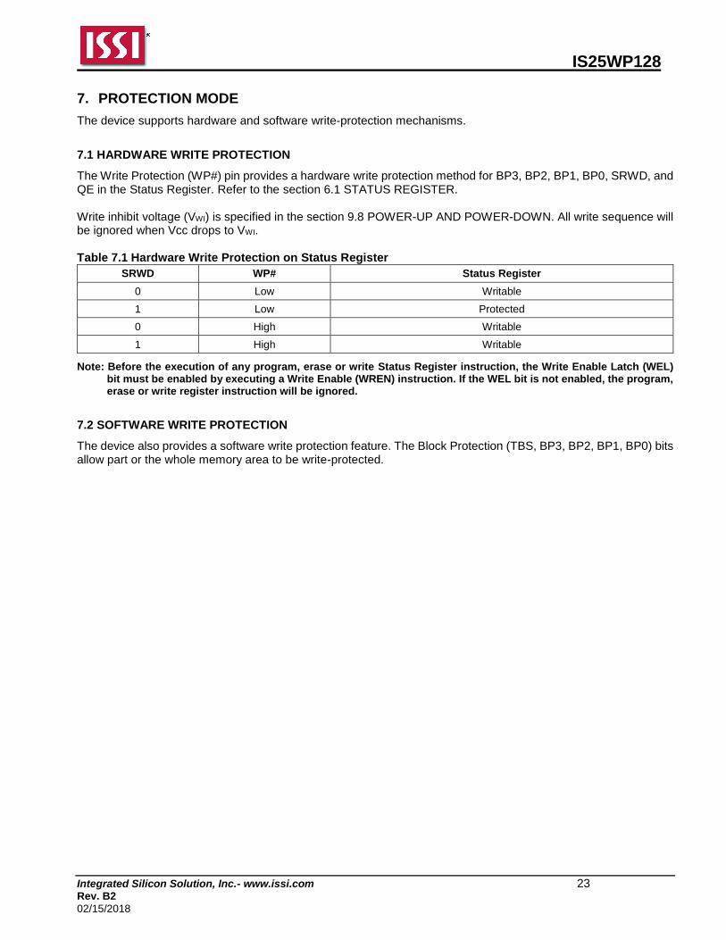
7. PROTECTION MODE................................................................................................................................... 23
7.1 HARDWARE WRITE PROTECTION...................................................................................................... 23
7.2 SOFTWARE WRITE PROTECTION ...................................................................................................... 23
8. DEVICE OPERATION .................................................................................................................................. 24
8.1 NORMAL READ OPERATION (NORD, 03h) ......................................................................................... 27
8.2 FAST READ OPERATION (FRD, 0Bh) .................................................................................................. 29
8.3 HOLD OPERATION ................................................................................................................................ 31
8.4 FAST READ DUAL I/O OPERATION (FRDIO, BBh) ............................................................................. 31
8.5 FAST READ DUAL OUTPUT OPERATION (FRDO, 3Bh) ..................................................................... 34
8.6 FAST READ QUAD OUTPUT OPERATION (FRQO, 6Bh).................................................................... 35
8.7 FAST READ QUAD I/O OPERATION (FRQIO, EBh) ............................................................................ 37
8.8 PAGE PROGRAM OPERATION (PP, 02h) ............................................................................................ 41
8.9 QUAD INPUT PAGE PROGRAM OPERATION (PPQ, 32h/38h) .......................................................... 43
8.10 ERASE OPERATION ........................................................................................................................... 44
8.11 SECTOR ERASE OPERATION (SER, D7h/20h) ................................................................................. 45
8.12 BLOCK ERASE OPERATION (BER32K:52h, BER64K:D8h) .............................................................. 46
8.13 CHIP ERASE OPERATION (CER, C7h/60h) ....................................................................................... 48
8.14 WRITE ENABLE OPERATION (WREN, 06h) ...................................................................................... 49
8.15 WRITE DISABLE OPERATION (WRDI, 04h) ....................................................................................... 50
8.16 READ STATUS REGISTER OPERATION (RDSR, 05h) ..................................................................... 51
8.17 WRITE STATUS REGISTER OPERATION (WRSR, 01h) ................................................................... 52
8.18 READ FUNCTION REGISTER OPERATION (RDFR, 48h) ................................................................. 53
8.19 WRITE FUNCTION REGISTER OPERATION (WRFR, 42h)............................................................... 54
8.20 ENTER QUAD PERIPHERAL INTERFACE (QPI) MODE OPERATION (QPIEN,35h; QPIDI,F5h) .... 55
IS25WP128
Integrated Silicon Solution, Inc.- www.issi.com 5 Rev. B2
02/15/2018
8.21 PROGRAM/ERASE SUSPEND & RESUME ........................................................................................ 56
8.22 ENTER DEEP POWER DOWN (DP, B9h) ........................................................................................... 58
8.23 RELEASE DEEP POWER DOWN (RDPD, ABh) ................................................................................. 59
8.24 SET READ PARAMETERS OPERATION (SRPNV: 65h, SRPV: C0h/63h) ........................................ 60
8.25 SET EXTENDED READ PARAMETERS OPERATION (SERPNV: 85h, SERPV: 83h) ...................... 62
8.26 READ READ PARAMETERS OPERATION (RDRPNV, 61h) .............................................................. 63
8.27 READ EXTENDED READ PARAMETERS OPERATION (RDERPNV, 81h) ....................................... 64
8.28 READ PRODUCT IDENTIFICATION (RDID, ABh) .............................................................................. 65
8.29 READ JEDEC ID OPERATION (RDJDID, 9Fh; RDJDIDQ, AFh) ........................................................ 67
8.30 READ DEVICE MANUFACTURER AND DEVICE ID OPERATION (RDMDID, 90h) .......................... 68
8.31 READ UNIQUE ID NUMBER (RDUID, 4Bh) ........................................................................................ 69
8.32 READ SFDP OPERATION (RDSFDP, 5Ah) ........................................................................................ 70
8.33 NO OPERATION (NOP, 00h) ............................................................................................................... 70
8.34 SOFTWARE RESET (RESET-ENABLE (RSTEN, 66h) AND RESET (RST, 99h)) AND HARDWARE RESET .......................................................................................................................................................... 71
8.35 SECURITY INFORMATION ROW ........................................................................................................ 72
8.36 INFORMATION ROW ERASE OPERATION (IRER, 64h) ................................................................... 73
8.37 INFORMATION ROW PROGRAM OPERATION (IRP, 62h) ............................................................... 74
8.38 INFORMATION ROW READ OPERATION (IRRD, 68h) ..................................................................... 75
8.39 FAST READ DTR MODE OPERATION IN SPI MODE (FRDTR, 0Dh) ............................................... 76
8.40 FAST READ DUAL IO DTR MODE OPERATION (FRDDTR, BDh) .................................................... 78
8.41 FAST READ QUAD IO DTR MODE OPERATION IN SPI MODE (FRQDTR, EDh) ............................ 81
8.42 SECTOR LOCK/UNLOCK FUNCTIONS .............................................................................................. 85
8.43 AUTOBOOT .......................................................................................................................................... 87
9. ELECTRICAL CHARACTERISTICS ............................................................................................................. 91
9.1 ABSOLUTE MAXIMUM RATINGS (1) ..................................................................................................... 91
9.2 OPERATING RANGE ............................................................................................................................. 91
9.3 DC CHARACTERISTICS ........................................................................................................................ 92
9.4 AC MEASUREMENT CONDITIONS ...................................................................................................... 93
9.5 PIN CAPACITANCE (TA = 25°C, VCC=3V, 1MHz) ............................................................................... 93
9.6 AC CHARACTERISTICS ........................................................................................................................ 94
9.7 SERIAL INPUT/OUTPUT TIMING .......................................................................................................... 96
9.8 POWER-UP AND POWER-DOWN ........................................................................................................ 98
9.9 PROGRAM/ERASE PERFORMANCE ................................................................................................... 99
9.10 RELIABILITY CHARACTERISTICS ..................................................................................................... 99
10. PACKAGE TYPE INFORMATION ......................................................................................................... 100
10.1 8-Pin JEDEC 208mil Broad Small Outline Integrated Circuit (SOIC) Package (B) ............................ 100
10.2 8-Contact Ultra-Thin Small Outline No-Lead (WSON) Package 6x5mm (K)...................................... 101
10.3 8-Contact Ultra-Thin Small Outline No-Lead (WSON) Package 8x6mm (L) ...................................... 102
10.4 16-lead Plastic Small Outline package (300 mils body width) (M) ..................................................... 103
IS25WP128
Integrated Silicon Solution, Inc.- www.issi.com 6 Rev. B2
02/15/2018
10.5 24-Ball Thin Profile Fine Pitch BGA 6x8mm 4x6 BALL ARRAY (G) .................................................. 104
10.6 24-Ball Thin Profile Fine Pitch BGA 6x8mm 5x5 BALL ARRAY (H) ................................................... 105
11. ORDERING INFORMATION – Valid Part Numbers .............................................................................. 106
IS25WP128
Integrated Silicon Solution, Inc.- www.issi.com 7 Rev. B2
02/15/2018
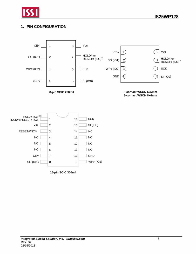
1. PIN CONFIGURATION
HOLD# or RESET# (IO3)
Vcc CE#
GND
SCK
1
2
3
4
7
6
5
SO (IO1)
SI (IO0)
8
WP# (IO2) 6 3
CE# Vcc
SCK
SI (IO0)
7
8
5 4
1
2
GND
WP# (IO2)
SO (IO1) HOLD# or RESET# (IO3)
8-pin SOIC 208mil 8-contact WSON 6x5mm
8-contact WSON 8x6mm
(1) (1)
(1,2)
16-pin SOIC 300mil
12
10
11
9
13
15
14
5
7
6
8
4
2
3
16 1
Vcc
HOLD# (IO3) HOLD# or RESET# (IO3) SCK
CE#
WP# (IO2)
GND
NC
NC
NC
NC
NC
SI (IO0)
SO (IO1)
NC
NC
RESET#/NC(3)
IS25WP128
Integrated Silicon Solution, Inc.- www.issi.com 8 Rev. B2
02/15/2018
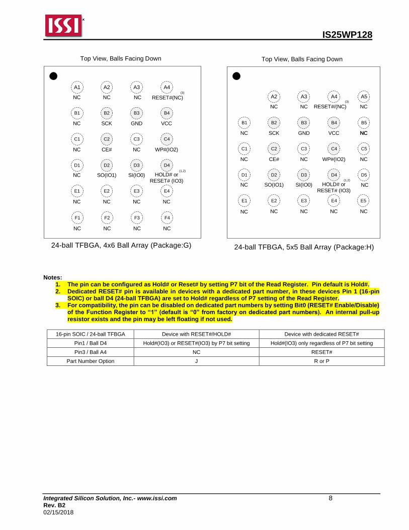
Top View, Balls Facing Down
NC NC NC NC
F1 F2 F3 F4
NC RESET#(NC)
NC SCK GND VCC
NC CE# NC WP#(IO2)
NC SO(IO1) SI(IO0) HOLD# or
RESET# (IO3)
NC NC NC NC
NC
A2 A3 A4
B1 B2 B3 B4
C1 C2 C3 C4
D1 D2 D3 D4
E1 E2 E3 E4
A1(3)
(1,2)
24-ball TFBGA, 4x6 Ball Array (Package:G)
NC NC RESET#/(NC)
NC SCK GND VCC
NC CE# NC WP#(IO2)
NC SO(IO1) SI(IO0) HOLD# or
RESET# (IO3)
NC NC NC NC
NC
NC
NC
NC
Top View, Balls Facing Down
NC
24-ball TFBGA, 5x5 Ball Array (Package:H)
A2 A3 A4
B1 B2 B3 B4
C1 C2 C3 C4
D1 D2 D3 D4
E1 E2 E3 E4
A5
B5
C5
D5
E5
NC
(3)
(1,2)
NC
Notes:
1. The pin can be configured as Hold# or Reset# by setting P7 bit of the Read Register. Pin default is Hold#. 2. Dedicated RESET# pin is available in devices with a dedicated part number, in these devices Pin 1 (16-pin
SOIC) or ball D4 (24-ball TFBGA) are set to Hold# regardless of P7 setting of the Read Register. 3. For compatibility, the pin can be disabled on dedicated part numbers by setting Bit0 (RESET# Enable/Disable)
of the Function Register to “1” (default is “0” from factory on dedicated part numbers). An internal pull-up resistor exists and the pin may be left floating if not used.
16-pin SOIC / 24-ball TFBGA Device with RESET#/HOLD# Device with dedicated RESET#
Pin1 / Ball D4 Hold#(IO3) or RESET#(IO3) by P7 bit setting Hold#(IO3) only regardless of P7 bit setting
Pin3 / Ball A4 NC RESET#
Part Number Option J R or P
IS25WP128
Integrated Silicon Solution, Inc.- www.issi.com 9 Rev. B2
02/15/2018
2. PIN DESCRIPTIONS
For the device with RESET#/Hold#
SYMBOL TYPE DESCRIPTION
CE# INPUT
Chip Enable: The Chip Enable (CE#) pin enables and disables the devices
operation. When CE# is high the device is deselected and output pins are in a high impedance state. When deselected the devices non-critical internal circuitry power down to allow minimal levels of power consumption while in a standby state.
When CE# is pulled low the device will be selected and brought out of standby mode. The device is considered active and instructions can be written to, data read, and written to the device. After power-up, CE# must transition from high to low before a new instruction will be accepted.
Keeping CE# in a high state deselects the device and switches it into its low power state. Data will not be accepted when CE# is high.
SI (IO0), SO (IO1)
INPUT/OUTPUT
Serial Data Input, Serial Output, and IOs (SI, SO, IO0, and IO1):
This device supports standard SPI, Dual SPI, and Quad SPI operation. Standard SPI instructions use the unidirectional SI (Serial Input) pin to write instructions, addresses, or data to the device on the rising edge of the Serial Clock (SCK). Standard SPI also uses the unidirectional SO (Serial Output) to read data or status from the device on the falling edge of the serial clock (SCK).
In Dual and Quad SPI mode, SI and SO become bidirectional IO pins to write instructions, addresses or data to the device on the rising edge of the Serial Clock (SCK) and read data or status from the device on the falling edge of SCK. Quad SPI instructions use the WP# and HOLD# pins as IO2 and IO3 respectively.
WP# (IO2) INPUT/OUTPUT
Write Protect/Serial Data IO (IO2): The WP# pin protects the Status Register from
being written in conjunction with the SRWD bit. When the SRWD is set to “1” and the WP# is pulled low, the Status Register bits (SRWD, QE, BP3, BP2, BP1, BP0) are write-protected and vice-versa for WP# high. When the SRWD is set to “0”, the Status Register is not write-protected regardless of WP# state.
When the QE bit is set to “1”, the WP# pin (Write Protect) function is not available since this pin is used for IO2.
HOLD# or RESET# (IO3)
INPUT/OUTPUT
HOLD# or RESET#/Serial Data IO (IO3): When the QE bit of Status Register is set
to “1”, HOLD# pin or RESET# is not available since it becomes IO3. When QE=0, the pin acts as HOLD# or RESET# and either one can be selected by the P7 bit setting in Read Register. HOLD# will be selected if P7=0 (Default) and RESET# will be selected if P7=1.
The HOLD# pin allows the device to be paused while it is selected. It pauses serial communication by the master device without resetting the serial sequence. The HOLD# pin is active low. When HOLD# is in a low state and CE# is low, the SO pin will be at high impedance. Device operation can resume when HOLD# pin is brought to a high state.
RESET# pin is a hardware RESET signal. When RESET# is driven HIGH, the memory is in the normal operating mode. When RESET# is driven LOW, the memory enters reset mode and output is High-Z. If RESET# is driven LOW while an internal WRITE, PROGRAM, or ERASE operation is in progress, data may be lost.
SCK INPUT Serial Data Clock: Synchronized Clock for input and output timing operations.
Vcc POWER Power: Device Core Power Supply
GND GROUND Ground: Connect to ground when referenced to Vcc
NC Unused NC: Pins labeled “NC” stand for “No Connect” and should be left unconnected.
IS25WP128
Integrated Silicon Solution, Inc.- www.issi.com 10 Rev. B2
02/15/2018
For the device with a dedicated RESET#
SYMBOL TYPE DESCRIPTION
CE# INPUT Same as the description in previous page
SI (IO0), SO (IO1)
INPUT/OUTPUT Same as the description in previous page
WP# (IO2) INPUT/OUTPUT Same as the description in previous page
HOLD# (IO3) INPUT/OUTPUT
HOLD#/Serial Data IO (IO3): When the QE bit of Status Register is set to “1”, HOLD#
pin is not available since it becomes IO3. When QE=0 the pin acts as HOLD# regardless of the P7 bit of Read Register.
The HOLD# pin allows the device to be paused while it is selected. It pauses serial communication by the master device without resetting the serial sequence. The HOLD# pin is active low. When HOLD# is in a low state and CE# is low, the SO pin will be at high impedance. Device operation can resume when HOLD# pin is brought to a high state.
RESET# INPUT/OUTPUT
RESET#: This additional RESET# pin is available only for dedicated parts.
The RESET# pin is a hardware RESET signal. When RESET# is driven HIGH, the memory is in the normal operating mode. When RESET# is driven LOW, the memory enters reset mode and output is High-Z. If RESET# is driven LOW while an internal WRITE, PROGRAM, or ERASE operation is in progress, data may be lost.
SCK INPUT Same as the description in previous page
Vcc POWER Same as the description in previous page
GND GROUND Same as the description in previous page
NC Unused Same as the description in previous page
IS25WP128
Integrated Silicon Solution, Inc.- www.issi.com 11 Rev. B2
02/15/2018
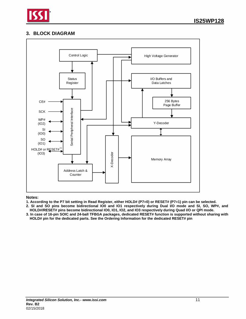
3. BLOCK DIAGRAM
Notes: 1. According to the P7 bit setting in Read Register, either HOLD# (P7=0) or RESET# (P7=1) pin can be selected. 2. SI and SO pins become bidirectional IO0 and IO1 respectively during Dual I/O mode and SI, SO, WP#, and
HOLD#/RESET# pins become bidirectional IO0, IO1, IO2, and IO3 respectively during Quad I/O or QPI mode. 3. In case of 16-pin SOIC and 24-ball TFBGA packages, dedicated RESET# function is supported without sharing with
HOLD# pin for the dedicated parts. See the Ordering Information for the dedicated RESET# pin
Control Logic High Voltage Generator
I/O Buffers and
Data Latches
256 Bytes
Page Buffer
Y-Decoder
X-D
eco
der
Se
ria
l P
erip
hera
l In
terf
ace
Status
Register
Address Latch &
Counter
Memory Array
CE#
SCK
WP#
(IO2)
SI
(IO0)
SO
(IO1)
HOLD# or RESET#
(IO3)
WP# (IO2)
(1)
IS25WP128
Integrated Silicon Solution, Inc.- www.issi.com 12 Rev. B2
02/15/2018
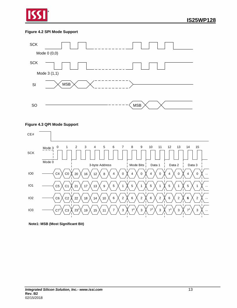
4. SPI MODES DESCRIPTION
Multiple IS25WP128 device can be connected on the SPI serial bus and controlled by a SPI Master, i.e. microcontroller, as shown in Figure 4.1. The devices support either of two SPI modes:
Mode 0 (0, 0) Mode 3 (1, 1)
The difference between these two modes is the clock polarity. When the SPI master is in stand-by mode, the serial clock remains at “0” (SCK = 0) for Mode 0 and the clock remains at “1” (SCK = 1) for Mode 3. Please refer to Figure 4.2 and Figure 4.3 for SPI and QPI mode. In both modes, the input data is latched on the rising edge of Serial Clock (SCK), and the output data is available from the falling edge of SCK. Figure 4.1 Connection Diagram among SPI Master and SPI Slaves (Memory Devices)
SPI interface with
(0,0) or (1,1)
SPI Master
(i.e. Microcontroller)SPI
Memory
Device
SPI
Memory
Device
SPI
Memory
Device
SCK SO SI
SCK
SDI
SDO
CE#
WP#
SCK SO SI
CE#
WP#
SCK SO SI
CE#
WP# HOLD#
or RESET#
CS3 CS2 CS1
HOLD#
or RESET#
HOLD#
or RESET#
Notes: 1. According to the P7 bit setting in Read Register, either HOLD# (P7=0) or RESET# (P7=1) pin can be selected. 2. SI and SO pins become bidirectional IO0 and IO1 respectively during Dual I/O mode and SI, SO, WP#, and
RESET#/HOLD# pins become bidirectional IO0, IO1, IO2, and IO3 respectively during Quad I/O or QPI mode. 3. In case of 16-pin SOIC and 24-ball TFBGA packages, dedicated RESET# function is supported without sharing with
HOLD# pin for the dedicated parts. See the Ordering Information for the dedicated RESET# pin
IS25WP128
Integrated Silicon Solution, Inc.- www.issi.com 13 Rev. B2
02/15/2018
Figure 4.2 SPI Mode Support
SCK
SO
SI
Mode 0 (0,0)
Mode 3 (1,1)
MSB
MSB
SCK
Figure 4.3 QPI Mode Support
20
CE#
SCK
4 0 4 0
3-byte Address
16 12 8
0 1 2 3 4 5 6 7 8 9 10 11 12 13 14 15Mode 3
Mode 0
IO0
IO1 21 5 1 5 117 13 9
22 6 2 6 218 14 10
7 3 319 15 11
Mode Bits
IO2
IO3
C4 C0
C1C5
C2C6
C3C71
4 0 4 0
5 1 5 1
6 2 6 2
3 3
4
5
6
0
1
2
3
...
...
...
...
Data 1 Data 2 Data 3
231
71 7
17
1 71
6
Note1: MSB (Most Significant Bit)
IS25WP128
Integrated Silicon Solution, Inc.- www.issi.com 14 Rev. B2
02/15/2018
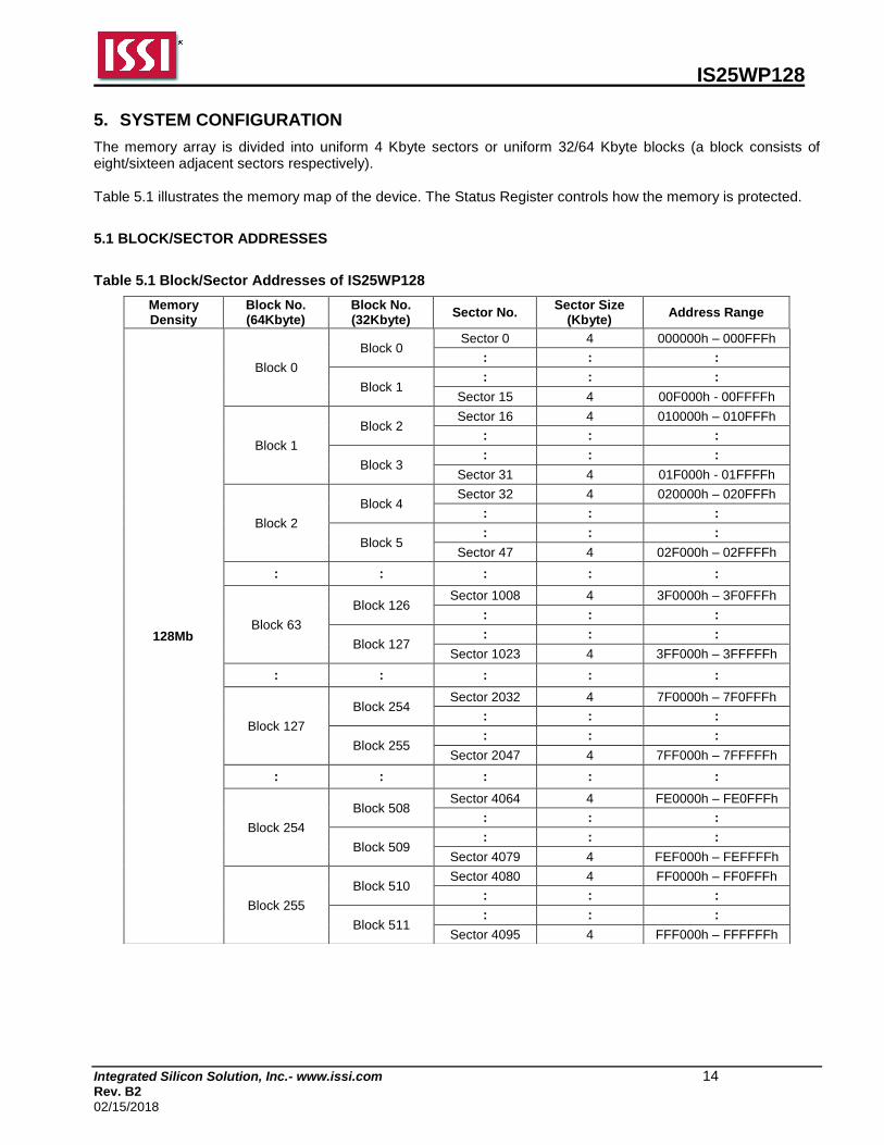
5. SYSTEM CONFIGURATION
The memory array is divided into uniform 4 Kbyte sectors or uniform 32/64 Kbyte blocks (a block consists of eight/sixteen adjacent sectors respectively). Table 5.1 illustrates the memory map of the device. The Status Register controls how the memory is protected.
5.1 BLOCK/SECTOR ADDRESSES
Table 5.1 Block/Sector Addresses of IS25WP128
Memory Density
Block No. (64Kbyte)
Block No. (32Kbyte)
Sector No. Sector Size
(Kbyte) Address Range
128Mb
Block 0
Block 0 Sector 0 4 000000h – 000FFFh
: : :
Block 1 : : :
Sector 15 4 00F000h - 00FFFFh
Block 1
Block 2 Sector 16 4 010000h – 010FFFh
: : :
Block 3 : : :
Sector 31 4 01F000h - 01FFFFh
Block 2
Block 4 Sector 32 4 020000h – 020FFFh
: : :
Block 5 : : :
Sector 47 4 02F000h – 02FFFFh
: : : : :
Block 63
Block 126 Sector 1008 4 3F0000h – 3F0FFFh
: : :
Block 127 : : :
Sector 1023 4 3FF000h – 3FFFFFh
: : : : :
Block 127
Block 254 Sector 2032 4 7F0000h – 7F0FFFh
: : :
Block 255 : : :
Sector 2047 4 7FF000h – 7FFFFFh
: : : : :
Block 254
Block 508 Sector 4064 4 FE0000h – FE0FFFh
: : :
Block 509 : : :
Sector 4079 4 FEF000h – FEFFFFh
Block 255
Block 510 Sector 4080 4 FF0000h – FF0FFFh
: : :
Block 511 : : :
Sector 4095 4 FFF000h – FFFFFFh
IS25WP128
Integrated Silicon Solution, Inc.- www.issi.com 15 Rev. B2
02/15/2018
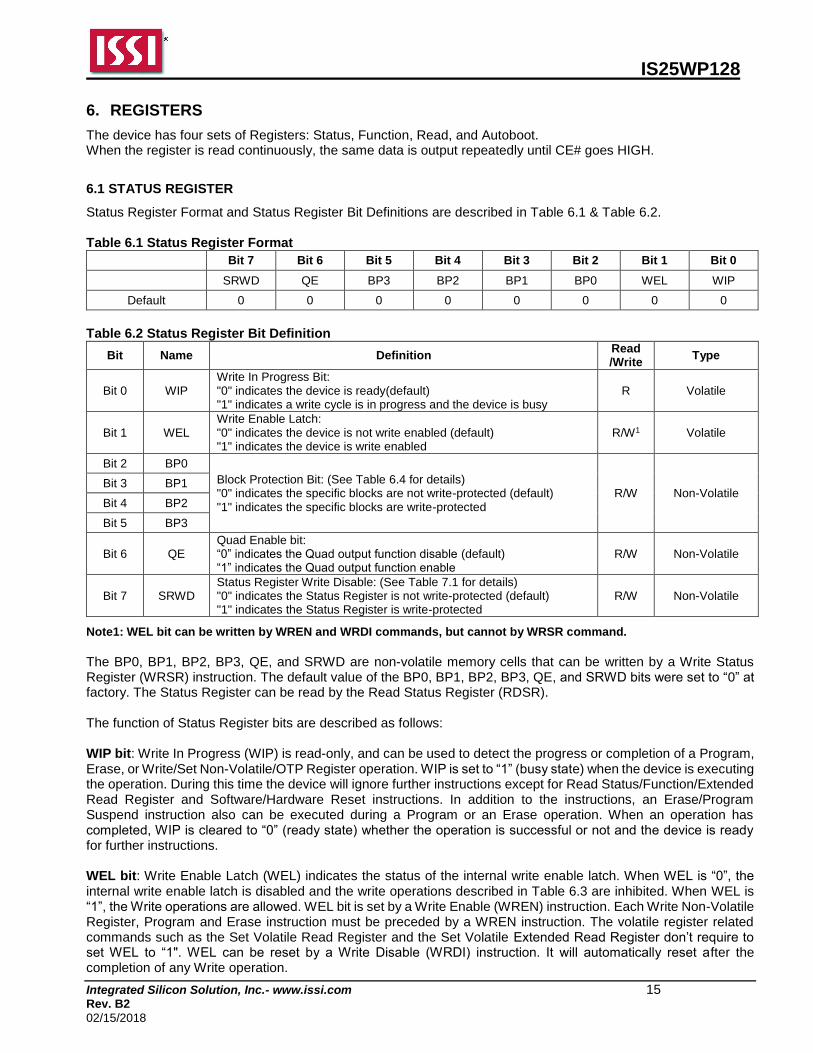
6. REGISTERS
The device has four sets of Registers: Status, Function, Read, and Autoboot. When the register is read continuously, the same data is output repeatedly until CE# goes HIGH.
6.1 STATUS REGISTER
Status Register Format and Status Register Bit Definitions are described in Table 6.1 & Table 6.2. Table 6.1 Status Register Format
Bit 7 Bit 6 Bit 5 Bit 4 Bit 3 Bit 2 Bit 1 Bit 0
SRWD QE BP3 BP2 BP1 BP0 WEL WIP
Default 0 0 0 0 0 0 0 0
Table 6.2 Status Register Bit Definition
Bit Name Definition Read /Write
Type
Bit 0 WIP Write In Progress Bit: "0" indicates the device is ready(default) "1" indicates a write cycle is in progress and the device is busy
R Volatile
Bit 1 WEL Write Enable Latch: "0" indicates the device is not write enabled (default) "1" indicates the device is write enabled
R/W1 Volatile
Bit 2 BP0
Block Protection Bit: (See Table 6.4 for details) "0" indicates the specific blocks are not write-protected (default) "1" indicates the specific blocks are write-protected
R/W Non-Volatile Bit 3 BP1
Bit 4 BP2
Bit 5 BP3
Bit 6 QE Quad Enable bit: “0” indicates the Quad output function disable (default) “1” indicates the Quad output function enable
R/W Non-Volatile
Bit 7 SRWD Status Register Write Disable: (See Table 7.1 for details) "0" indicates the Status Register is not write-protected (default) "1" indicates the Status Register is write-protected
R/W Non-Volatile
Note1: WEL bit can be written by WREN and WRDI commands, but cannot by WRSR command. The BP0, BP1, BP2, BP3, QE, and SRWD are non-volatile memory cells that can be written by a Write Status Register (WRSR) instruction. The default value of the BP0, BP1, BP2, BP3, QE, and SRWD bits were set to “0” at factory. The Status Register can be read by the Read Status Register (RDSR). The function of Status Register bits are described as follows: WIP bit: Write In Progress (WIP) is read-only, and can be used to detect the progress or completion of a Program, Erase, or Write/Set Non-Volatile/OTP Register operation. WIP is set to “1” (busy state) when the device is executing the operation. During this time the device will ignore further instructions except for Read Status/Function/Extended Read Register and Software/Hardware Reset instructions. In addition to the instructions, an Erase/Program Suspend instruction also can be executed during a Program or an Erase operation. When an operation has completed, WIP is cleared to “0” (ready state) whether the operation is successful or not and the device is ready for further instructions. WEL bit: Write Enable Latch (WEL) indicates the status of the internal write enable latch. When WEL is “0”, the internal write enable latch is disabled and the write operations described in Table 6.3 are inhibited. When WEL is “1”, the Write operations are allowed. WEL bit is set by a Write Enable (WREN) instruction. Each Write Non-Volatile Register, Program and Erase instruction must be preceded by a WREN instruction. The volatile register related commands such as the Set Volatile Read Register and the Set Volatile Extended Read Register don’t require to set WEL to “1". WEL can be reset by a Write Disable (WRDI) instruction. It will automatically reset after the completion of any Write operation.
IS25WP128
Integrated Silicon Solution, Inc.- www.issi.com 16 Rev. B2
02/15/2018
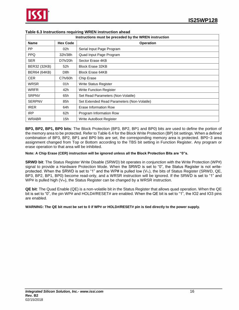
Table 6.3 Instructions requiring WREN instruction ahead
Instructions must be preceded by the WREN instruction
Name Hex Code Operation
PP 02h Serial Input Page Program
PPQ 32h/38h Quad Input Page Program
SER D7h/20h Sector Erase 4KB
BER32 (32KB) 52h Block Erase 32KB
BER64 (64KB) D8h Block Erase 64KB
CER C7h/60h Chip Erase
WRSR 01h Write Status Register
WRFR 42h Write Function Register
SRPNV 65h Set Read Parameters (Non-Volatile)
SERPNV 85h Set Extended Read Parameters (Non-Volatile)
IRER 64h Erase Information Row
IRP 62h Program Information Row
WRABR 15h Write AutoBoot Register
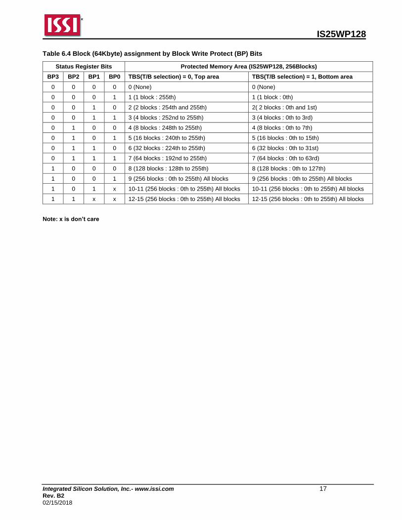
BP3, BP2, BP1, BP0 bits: The Block Protection (BP3, BP2, BP1 and BP0) bits are used to define the portion of the memory area to be protected. Refer to Table 6.4 for the Block Write Protection (BP) bit settings. When a defined combination of BP3, BP2, BP1 and BP0 bits are set, the corresponding memory area is protected. BP0~3 area assignment changed from Top or Bottom according to the TBS bit setting in Function Register. Any program or erase operation to that area will be inhibited.
Note: A Chip Erase (CER) instruction will be ignored unless all the Block Protection Bits are “0”s.
SRWD bit: The Status Register Write Disable (SRWD) bit operates in conjunction with the Write Protection (WP#) signal to provide a Hardware Protection Mode. When the SRWD is set to “0”, the Status Register is not write-protected. When the SRWD is set to “1” and the WP# is pulled low (VIL), the bits of Status Register (SRWD, QE, BP3, BP2, BP1, BP0) become read-only, and a WRSR instruction will be ignored. If the SRWD is set to “1” and WP# is pulled high (VIH), the Status Register can be changed by a WRSR instruction. QE bit: The Quad Enable (QE) is a non-volatile bit in the Status Register that allows quad operation. When the QE bit is set to “0”, the pin WP# and HOLD#/RESET# are enabled. When the QE bit is set to “1”, the IO2 and IO3 pins are enabled. WARNING: The QE bit must be set to 0 if WP# or HOLD#/RESET# pin is tied directly to the power supply.
IS25WP128
Integrated Silicon Solution, Inc.- www.issi.com 17 Rev. B2
02/15/2018
Table 6.4 Block (64Kbyte) assignment by Block Write Protect (BP) Bits
Status Register Bits Protected Memory Area (IS25WP128, 256Blocks)
BP3 BP2 BP1 BP0 TBS(T/B selection) = 0, Top area TBS(T/B selection) = 1, Bottom area
0 0 0 0 0 (None) 0 (None)
0 0 0 1 1 (1 block : 255th) 1 (1 block : 0th)
0 0 1 0 2 (2 blocks : 254th and 255th) 2( 2 blocks : 0th and 1st)
0 0 1 1 3 (4 blocks : 252nd to 255th) 3 (4 blocks : 0th to 3rd)
0 1 0 0 4 (8 blocks : 248th to 255th) 4 (8 blocks : 0th to 7th)
0 1 0 1 5 (16 blocks : 240th to 255th) 5 (16 blocks : 0th to 15th)
0 1 1 0 6 (32 blocks : 224th to 255th) 6 (32 blocks : 0th to 31st)
0 1 1 1 7 (64 blocks : 192nd to 255th) 7 (64 blocks : 0th to 63rd)
1 0 0 0 8 (128 blocks : 128th to 255th) 8 (128 blocks : 0th to 127th)
1 0 0 1 9 (256 blocks : 0th to 255th) All blocks 9 (256 blocks : 0th to 255th) All blocks
1 0 1 x 10-11 (256 blocks : 0th to 255th) All blocks 10-11 (256 blocks : 0th to 255th) All blocks
1 1 x x 12-15 (256 blocks : 0th to 255th) All blocks 12-15 (256 blocks : 0th to 255th) All blocks
Note: x is don’t care
IS25WP128
Integrated Silicon Solution, Inc.- www.issi.com 18 Rev. B2
02/15/2018
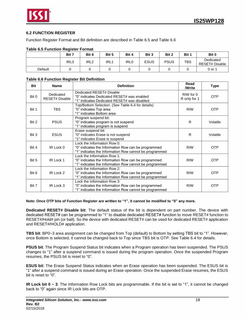
6.2 FUNCTION REGISTER
Function Register Format and Bit definition are described in Table 6.5 and Table 6.6 Table 6.5 Function Register Format
Bit 7 Bit 6 Bit 5 Bit 4 Bit 3 Bit 2 Bit 1 Bit 0
IRL3 IRL2 IRL1 IRL0 ESUS PSUS TBS Dedicated
RESET# Disable
Default 0 0 0 0 0 0 0 0 or 1
Table 6.6 Function Register Bit Definition
Bit Name Definition Read /Write
Type
Bit 0 Dedicated
RESET# Disable
Dedicated RESET# Disable “0” indicates Dedicated RESET# was enabled “1” indicates Dedicated RESET# was disabled
R/W for 0 R only for 1
OTP
Bit 1 TBS Top/Bottom Selection. (See Table 6.4 for details) “0” indicates Top area “1” indicates Bottom area
R/W OTP
Bit 2 PSUS Program suspend bit: “0” indicates program is not suspend “1” indicates program is suspend
R Volatile
Bit 3 ESUS Erase suspend bit: "0" indicates Erase is not suspend "1" indicates Erase is suspend
R Volatile
Bit 4
IR Lock 0
Lock the Information Row 0: “0” indicates the Information Row can be programmed “1” indicates the Information Row cannot be programmed
R/W OTP
Bit 5 IR Lock 1 Lock the Information Row 1: “0” indicates the Information Row can be programmed “1” indicates the Information Row cannot be programmed
R/W OTP
Bit 6 IR Lock 2 Lock the Information Row 2: “0” indicates the Information Row can be programmed “1” indicates the Information Row cannot be programmed
R/W OTP
Bit 7 IR Lock 3 Lock the Information Row 3: “0” indicates the Information Row can be programmed “1” indicates the Information Row cannot be programmed
R/W OTP
Note: Once OTP bits of Function Register are written to “1”, it cannot be modified to “0” any more.
Dedicated RESET# Disable bit: The default status of the bit is dependent on part number. The device with dedicated RESET# can be programmed to “1” to disable dedicated RESET# function to move RESET# function to RESET#/Hold# pin (or ball). So the device with dedicated RESET# can be used for dedicated RESET# application and RESET#/HOLD# application. TBS bit: BP0~3 area assignment can be changed from Top (default) to Bottom by setting TBS bit to “1”. However, once Bottom is selected, it cannot be changed back to Top since TBS bit is OTP. See Table 6.4 for details. PSUS bit: The Program Suspend Status bit indicates when a Program operation has been suspended. The PSUS changes to “1” after a suspend command is issued during the program operation. Once the suspended Program resumes, the PSUS bit is reset to “0”. ESUS bit: The Erase Suspend Status indicates when an Erase operation has been suspended. The ESUS bit is “1” after a suspend command is issued during an Erase operation. Once the suspended Erase resumes, the ESUS bit is reset to “0”. IR Lock bit 0 ~ 3: The Information Row Lock bits are programmable. If the bit is set to “1”, it cannot be changed back to “0” again since IR Lock bits are OTP.
IS25WP128
Integrated Silicon Solution, Inc.- www.issi.com 19 Rev. B2
02/15/2018
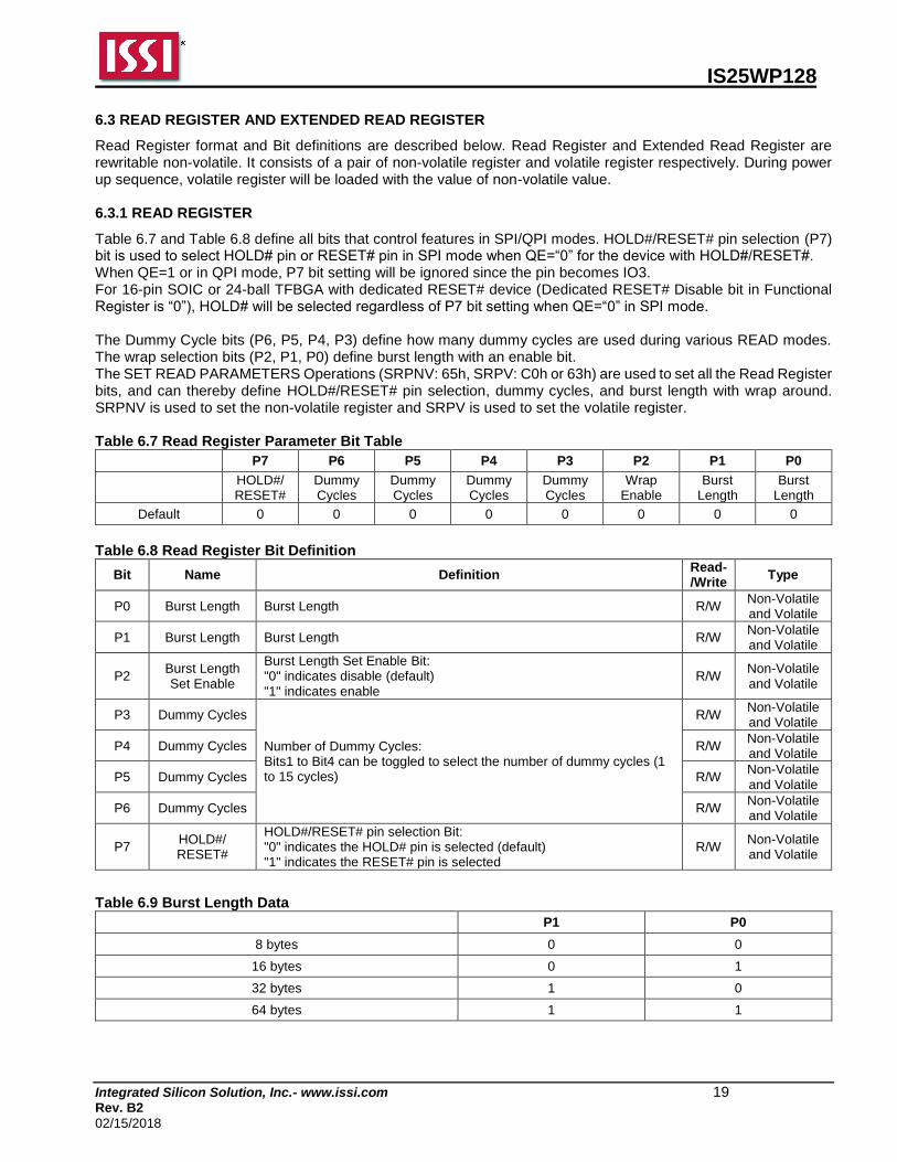
6.3 READ REGISTER AND EXTENDED READ REGISTER
Read Register format and Bit definitions are described below. Read Register and Extended Read Register are rewritable non-volatile. It consists of a pair of non-volatile register and volatile register respectively. During power up sequence, volatile register will be loaded with the value of non-volatile value. 6.3.1 READ REGISTER
Table 6.7 and Table 6.8 define all bits that control features in SPI/QPI modes. HOLD#/RESET# pin selection (P7) bit is used to select HOLD# pin or RESET# pin in SPI mode when QE=“0” for the device with HOLD#/RESET#. When QE=1 or in QPI mode, P7 bit setting will be ignored since the pin becomes IO3. For 16-pin SOIC or 24-ball TFBGA with dedicated RESET# device (Dedicated RESET# Disable bit in Functional Register is “0”), HOLD# will be selected regardless of P7 bit setting when QE=“0” in SPI mode. The Dummy Cycle bits (P6, P5, P4, P3) define how many dummy cycles are used during various READ modes. The wrap selection bits (P2, P1, P0) define burst length with an enable bit. The SET READ PARAMETERS Operations (SRPNV: 65h, SRPV: C0h or 63h) are used to set all the Read Register bits, and can thereby define HOLD#/RESET# pin selection, dummy cycles, and burst length with wrap around. SRPNV is used to set the non-volatile register and SRPV is used to set the volatile register. Table 6.7 Read Register Parameter Bit Table
P7 P6 P5 P4 P3 P2 P1 P0
HOLD#/ RESET#
Dummy Cycles
Dummy Cycles
Dummy Cycles
Dummy Cycles
Wrap Enable
Burst Length
Burst Length
Default 0 0 0 0 0 0 0 0
Table 6.8 Read Register Bit Definition
Bit Name Definition Read- /Write
Type
P0 Burst Length Burst Length R/W Non-Volatile and Volatile
P1 Burst Length Burst Length R/W Non-Volatile and Volatile
P2 Burst Length Set Enable
Burst Length Set Enable Bit: "0" indicates disable (default) "1" indicates enable
R/W Non-Volatile and Volatile
P3 Dummy Cycles
Number of Dummy Cycles: Bits1 to Bit4 can be toggled to select the number of dummy cycles (1 to 15 cycles)
R/W Non-Volatile and Volatile
P4 Dummy Cycles R/W Non-Volatile and Volatile
P5 Dummy Cycles R/W Non-Volatile and Volatile
P6 Dummy Cycles R/W Non-Volatile and Volatile
P7 HOLD#/ RESET#
HOLD#/RESET# pin selection Bit: "0" indicates the HOLD# pin is selected (default) "1" indicates the RESET# pin is selected
R/W Non-Volatile and Volatile
Table 6.9 Burst Length Data
P1 P0
8 bytes 0 0
16 bytes 0 1
32 bytes 1 0
64 bytes 1 1
IS25WP128
Integrated Silicon Solution, Inc.- www.issi.com 20 Rev. B2
02/15/2018
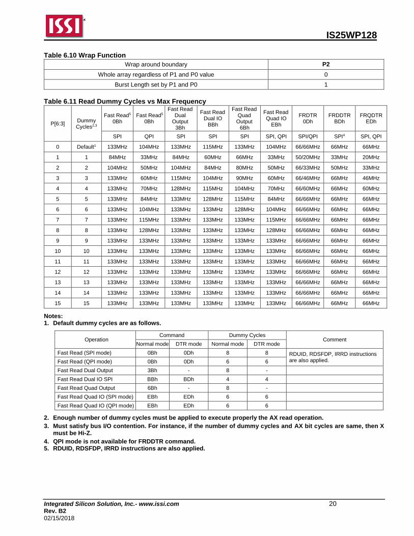
Table 6.10 Wrap Function
Wrap around boundary P2
Whole array regardless of P1 and P0 value 0
Burst Length set by P1 and P0 1
Table 6.11 Read Dummy Cycles vs Max Frequency
P[6:3] Dummy Cycles2,3
Fast Read5 0Bh
Fast Read5 0Bh
Fast Read Dual
Output 3Bh
Fast Read Dual IO
BBh
Fast Read Quad
Output 6Bh
Fast Read Quad IO
EBh
FRDTR 0Dh
FRDDTR BDh
FRQDTR EDh
SPI QPI SPI SPI SPI SPI, QPI SPI/QPI SPI4 SPI, QPI
0 Default1 133MHz 104MHz 133MHz 115MHz 133MHz 104MHz 66/66MHz 66MHz 66MHz
1 1 84MHz 33MHz 84MHz 60MHz 66MHz 33MHz 50/20MHz 33MHz 20MHz
2 2 104MHz 50MHz 104MHz 84MHz 80MHz 50MHz 66/33MHz 50MHz 33MHz
3 3 133MHz 60MHz 115MHz 104MHz 90MHz 60MHz 66/46MHz 66MHz 46MHz
4 4 133MHz 70MHz 128MHz 115MHz 104MHz 70MHz 66/60MHz 66MHz 60MHz
5 5 133MHz 84MHz 133MHz 128MHz 115MHz 84MHz 66/66MHz 66MHz 66MHz
6 6 133MHz 104MHz 133MHz 133MHz 128MHz 104MHz 66/66MHz 66MHz 66MHz
7 7 133MHz 115MHz 133MHz 133MHz 133MHz 115MHz 66/66MHz 66MHz 66MHz
8 8 133MHz 128MHz 133MHz 133MHz 133MHz 128MHz 66/66MHz 66MHz 66MHz
9 9 133MHz 133MHz 133MHz 133MHz 133MHz 133MHz 66/66MHz 66MHz 66MHz
10 10 133MHz 133MHz 133MHz 133MHz 133MHz 133MHz 66/66MHz 66MHz 66MHz
11 11 133MHz 133MHz 133MHz 133MHz 133MHz 133MHz 66/66MHz 66MHz 66MHz
12 12 133MHz 133MHz 133MHz 133MHz 133MHz 133MHz 66/66MHz 66MHz 66MHz
13 13 133MHz 133MHz 133MHz 133MHz 133MHz 133MHz 66/66MHz 66MHz 66MHz
14 14 133MHz 133MHz 133MHz 133MHz 133MHz 133MHz 66/66MHz 66MHz 66MHz
15 15 133MHz 133MHz 133MHz 133MHz 133MHz 133MHz 66/66MHz 66MHz 66MHz
Notes: 1. Default dummy cycles are as follows.
Operation Command Dummy Cycles
Comment Normal mode DTR mode Normal mode DTR mode
Fast Read (SPI mode) 0Bh 0Dh 8 8 RDUID, RDSFDP, IRRD instructions are also applied. Fast Read (QPI mode) 0Bh 0Dh 6 6
Fast Read Dual Output 3Bh - 8 -
Fast Read Dual IO SPI BBh BDh 4 4
Fast Read Quad Output 6Bh - 8 -
Fast Read Quad IO (SPI mode) EBh EDh 6 6
Fast Read Quad IO (QPI mode) EBh EDh 6 6
2. Enough number of dummy cycles must be applied to execute properly the AX read operation.
3. Must satisfy bus I/O contention. For instance, if the number of dummy cycles and AX bit cycles are same, then X must be Hi-Z.
4. QPI mode is not available for FRDDTR command. 5. RDUID, RDSFDP, IRRD instructions are also applied.
IS25WP128
Integrated Silicon Solution, Inc.- www.issi.com 21 Rev. B2
02/15/2018
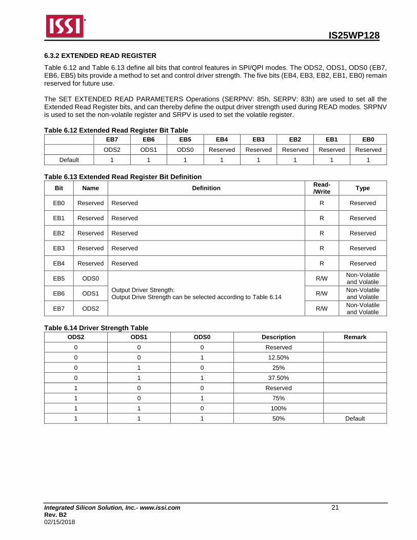
6.3.2 EXTENDED READ REGISTER
Table 6.12 and Table 6.13 define all bits that control features in SPI/QPI modes. The ODS2, ODS1, ODS0 (EB7, EB6, EB5) bits provide a method to set and control driver strength. The five bits (EB4, EB3, EB2, EB1, EB0) remain reserved for future use. The SET EXTENDED READ PARAMETERS Operations (SERPNV: 85h, SERPV: 83h) are used to set all the Extended Read Register bits, and can thereby define the output driver strength used during READ modes. SRPNV is used to set the non-volatile register and SRPV is used to set the volatile register. Table 6.12 Extended Read Register Bit Table
EB7 EB6 EB5 EB4 EB3 EB2 EB1 EB0
ODS2 ODS1 ODS0 Reserved Reserved Reserved Reserved Reserved
Default 1 1 1 1 1 1 1 1
Table 6.13 Extended Read Register Bit Definition
Bit Name Definition Read- /Write
Type
EB0 Reserved Reserved R Reserved
EB1 Reserved Reserved R Reserved
EB2 Reserved Reserved R Reserved
EB3 Reserved Reserved R Reserved
EB4 Reserved Reserved R Reserved
EB5 ODS0
Output Driver Strength: Output Drive Strength can be selected according to Table 6.14
R/W Non-Volatile and Volatile
EB6 ODS1 R/W Non-Volatile and Volatile
EB7 ODS2 R/W Non-Volatile and Volatile
Table 6.14 Driver Strength Table
ODS2 ODS1 ODS0 Description Remark
0 0 0 Reserved
0 0 1 12.50%
0 1 0 25%
0 1 1 37.50%
1 0 0 Reserved
1 0 1 75%
1 1 0 100%
1 1 1 50% Default
IS25WP128
Integrated Silicon Solution, Inc.- www.issi.com 22 Rev. B2
02/15/2018
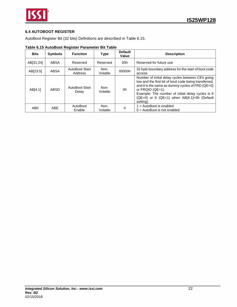
6.4 AUTOBOOT REGISTER
AutoBoot Register Bit (32 bits) Definitions are described in Table 6.15. Table 6.15 AutoBoot Register Parameter Bit Table
Bits Symbols Function Type Default Value
Description
AB[31:24] ABSA Reserved Reserved 00h Reserved for future use
AB[23:5] ABSA AutoBoot Start
Address Non-
Volatile 00000h
32 byte boundary address for the start of boot code access
AB[4:1] ABSD AutoBoot Start
Delay Non-
Volatile 0h
Number of initial delay cycles between CE# going low and the first bit of boot code being transferred, and it is the same as dummy cycles of FRD (QE=0) or FRQIO (QE=1). Example: The number of initial delay cycles is 8 (QE=0) or 6 (QE=1) when AB[4:1]=0h (Default setting).
AB0 ABE AutoBoot Enable
Non-Volatile
0 1 = AutoBoot is enabled 0 = AutoBoot is not enabled
IS25WP128
Integrated Silicon Solution, Inc.- www.issi.com 23 Rev. B2
02/15/2018
7. PROTECTION MODE
The device supports hardware and software write-protection mechanisms.
7.1 HARDWARE WRITE PROTECTION
The Write Protection (WP#) pin provides a hardware write protection method for BP3, BP2, BP1, BP0, SRWD, and QE in the Status Register. Refer to the section 6.1 STATUS REGISTER. Write inhibit voltage (VWI) is specified in the section 9.8 POWER-UP AND POWER-DOWN. All write sequence will be ignored when Vcc drops to VWI. Table 7.1 Hardware Write Protection on Status Register
SRWD WP# Status Register
0 Low Writable
1 Low Protected
0 High Writable
1 High Writable
Note: Before the execution of any program, erase or write Status Register instruction, the Write Enable Latch (WEL) bit must be enabled by executing a Write Enable (WREN) instruction. If the WEL bit is not enabled, the program, erase or write register instruction will be ignored.
7.2 SOFTWARE WRITE PROTECTION
The device also provides a software write protection feature. The Block Protection (TBS, BP3, BP2, BP1, BP0) bits allow part or the whole memory area to be write-protected.
IS25WP128
Integrated Silicon Solution, Inc.- www.issi.com 24 Rev. B2
02/15/2018
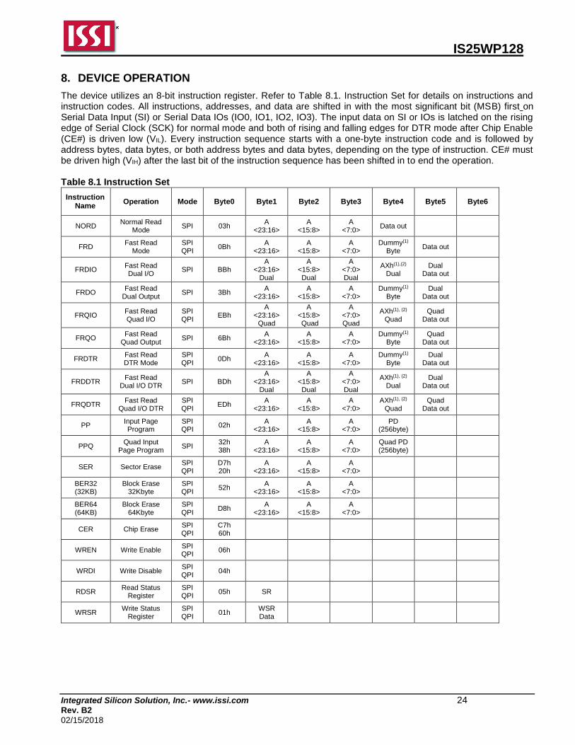
8. DEVICE OPERATION
The device utilizes an 8-bit instruction register. Refer to Table 8.1. Instruction Set for details on instructions and instruction codes. All instructions, addresses, and data are shifted in with the most significant bit (MSB) first on Serial Data Input (SI) or Serial Data IOs (IO0, IO1, IO2, IO3). The input data on SI or IOs is latched on the rising edge of Serial Clock (SCK) for normal mode and both of rising and falling edges for DTR mode after Chip Enable (CE#) is driven low (VIL). Every instruction sequence starts with a one-byte instruction code and is followed by address bytes, data bytes, or both address bytes and data bytes, depending on the type of instruction. CE# must be driven high (VIH) after the last bit of the instruction sequence has been shifted in to end the operation. Table 8.1 Instruction Set
Instruction Name
Operation Mode Byte0 Byte1 Byte2 Byte3 Byte4 Byte5 Byte6
NORD Normal Read
Mode SPI 03h
A <23:16>
A <15:8>
A <7:0>
Data out
FRD Fast Read
Mode SPI QPI
0Bh A
<23:16> A
<15:8> A
<7:0> Dummy(1)
Byte Data out
FRDIO Fast Read Dual I/O
SPI BBh A
<23:16> Dual
A <15:8> Dual
A <7:0> Dual
AXh(1),(2) Dual
Dual Data out
FRDO Fast Read
Dual Output SPI 3Bh
A <23:16>
A <15:8>
A <7:0>
Dummy(1) Byte
Dual Data out
FRQIO Fast Read Quad I/O
SPI QPI
EBh A
<23:16> Quad
A <15:8> Quad
A <7:0> Quad
AXh(1), (2) Quad
Quad Data out
FRQO Fast Read
Quad Output SPI 6Bh
A <23:16>
A <15:8>
A <7:0>
Dummy(1) Byte
Quad Data out
FRDTR Fast Read DTR Mode
SPI QPI
0Dh A
<23:16> A
<15:8> A
<7:0> Dummy(1)
Byte Dual
Data out
FRDDTR Fast Read
Dual I/O DTR SPI BDh
A <23:16>
Dual
A <15:8> Dual
A <7:0> Dual
AXh(1), (2) Dual
Dual Data out
FRQDTR Fast Read
Quad I/O DTR SPI QPI
EDh A
<23:16> A
<15:8> A
<7:0> AXh(1), (2)
Quad Quad
Data out
PP Input Page Program
SPI QPI
02h A
<23:16> A
<15:8> A
<7:0> PD
(256byte)
PPQ Quad Input
Page Program SPI
32h 38h
A <23:16>
A <15:8>
A <7:0>
Quad PD (256byte)
SER Sector Erase SPI QPI
D7h 20h
A <23:16>
A <15:8>
A <7:0>
BER32 (32KB)
Block Erase 32Kbyte
SPI QPI
52h A
<23:16> A
<15:8> A
<7:0>
BER64 (64KB)
Block Erase 64Kbyte
SPI QPI
D8h A
<23:16> A
<15:8> A
<7:0>
CER Chip Erase SPI QPI
C7h 60h
WREN Write Enable SPI QPI
06h
WRDI Write Disable SPI QPI
04h
RDSR Read Status
Register SPI QPI
05h SR
WRSR Write Status
Register SPI QPI
01h WSR Data
IS25WP128
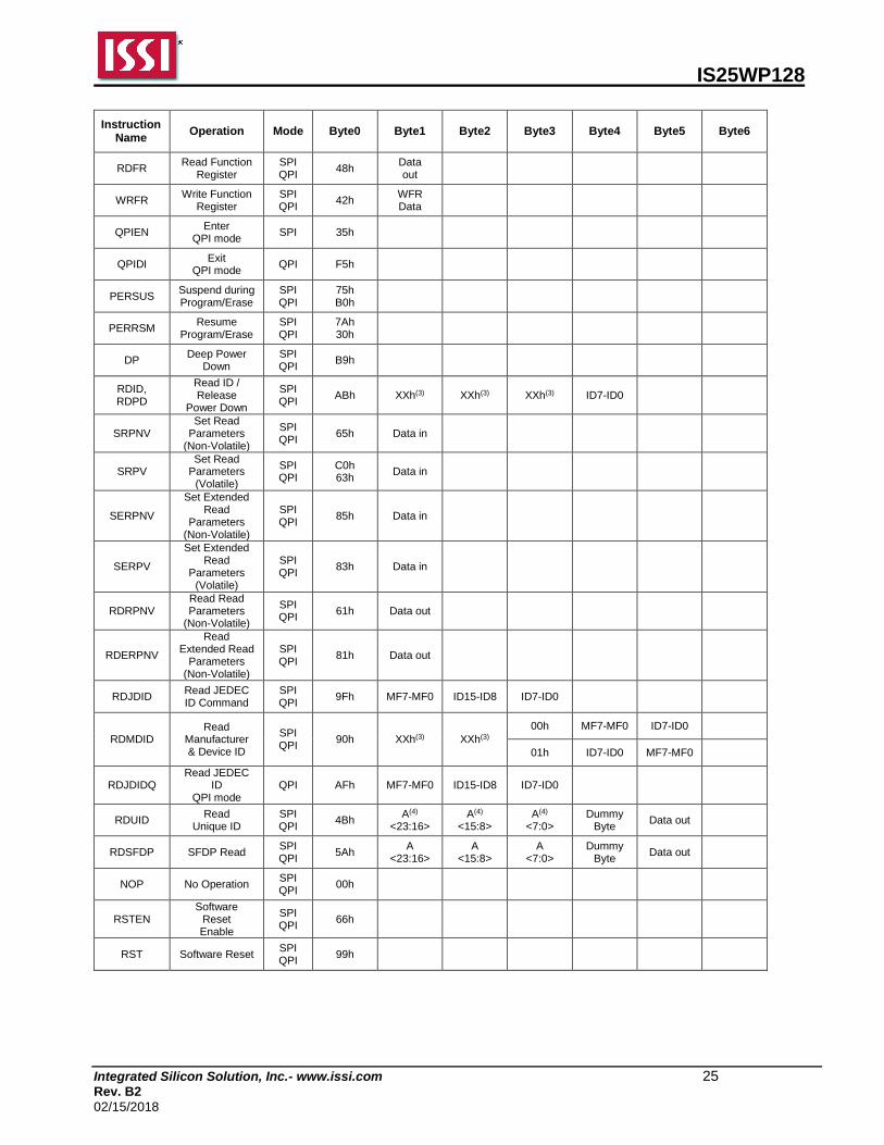
Integrated Silicon Solution, Inc.- www.issi.com 25 Rev. B2
02/15/2018
Instruction Name
Operation Mode Byte0 Byte1 Byte2 Byte3 Byte4 Byte5 Byte6
RDFR Read Function
Register SPI QPI
48h Data out
WRFR Write Function
Register SPI QPI
42h WFR Data
QPIEN Enter
QPI mode SPI 35h
QPIDI Exit
QPI mode QPI F5h
PERSUS Suspend during Program/Erase
SPI QPI
75h B0h
PERRSM Resume
Program/Erase SPI QPI
7Ah 30h
DP Deep Power
Down SPI QPI
B9h
RDID, RDPD
Read ID / Release
Power Down
SPI QPI
ABh XXh(3) XXh(3) XXh(3) ID7-ID0
SRPNV Set Read
Parameters (Non-Volatile)
SPI QPI
65h Data in
SRPV Set Read
Parameters (Volatile)
SPI QPI
C0h 63h
Data in
SERPNV
Set Extended Read
Parameters (Non-Volatile)
SPI QPI
85h Data in
SERPV
Set Extended Read
Parameters (Volatile)
SPI QPI
83h Data in
RDRPNV Read Read Parameters
(Non-Volatile)
SPI QPI
61h Data out
RDERPNV
Read Extended Read
Parameters (Non-Volatile)
SPI QPI
81h Data out
RDJDID Read JEDEC ID Command
SPI QPI
9Fh MF7-MF0 ID15-ID8 ID7-ID0
RDMDID Read
Manufacturer & Device ID
SPI QPI
90h XXh(3) XXh(3)
00h MF7-MF0 ID7-ID0
01h ID7-ID0 MF7-MF0
RDJDIDQ Read JEDEC
ID QPI mode
QPI AFh MF7-MF0 ID15-ID8 ID7-ID0
RDUID Read
Unique ID SPI QPI
4Bh A(4)
<23:16> A(4)
<15:8> A(4)
<7:0> Dummy
Byte Data out
RDSFDP SFDP Read SPI QPI
5Ah A
<23:16> A
<15:8> A
<7:0> Dummy
Byte Data out
NOP No Operation SPI QPI
00h
RSTEN Software
Reset Enable
SPI QPI
66h
RST Software Reset SPI QPI
99h

IS25WP128
Integrated Silicon Solution, Inc.- www.issi.com 26 Rev. B2
02/15/2018
Instruction Name
Operation Mode Byte0 Byte1 Byte2 Byte3 Byte4 Byte5 Byte6
IRER Erase
Information Row
SPI QPI
64h A
<23:16> A
<15:8> A
<7:0>
IRP Program
Information Row
SPI QPI
62h A
<23:16> A
<15:8> A
<7:0> PD
(256byte)
IRRD Read
Information Row
SPI QPI
68h A
<23:16> A
<15:8> A
<7:0> Dummy
Byte Data out
SECUN-LOCK
Sector Unlock SPI QPI
26h A
<23:16> A
<15:8> A
<7:0>
SECLOCK Sector Lock SPI QPI
24h
RDABR Read AutoBoot
Register SPI QPI
14h Data out 1 Data out 2 Data out 3 Data out 4
WRABR Write AutoBoot
Register SPI QPI
15h Data in 1 Data in 2 Data in 3 Data in 4
Notes: 1. The number of dummy cycles depends on the value setting in the Table 6.11 Read Dummy Cycles. 2. AXh has to be counted as a part of dummy cycles. X means “don’t care”. 3. XX means “don’t care”. 4. A<23:9> are “don’t care” and A<8:4> are always “0”.
IS25WP128
Integrated Silicon Solution, Inc.- www.issi.com 27 Rev. B2
02/15/2018
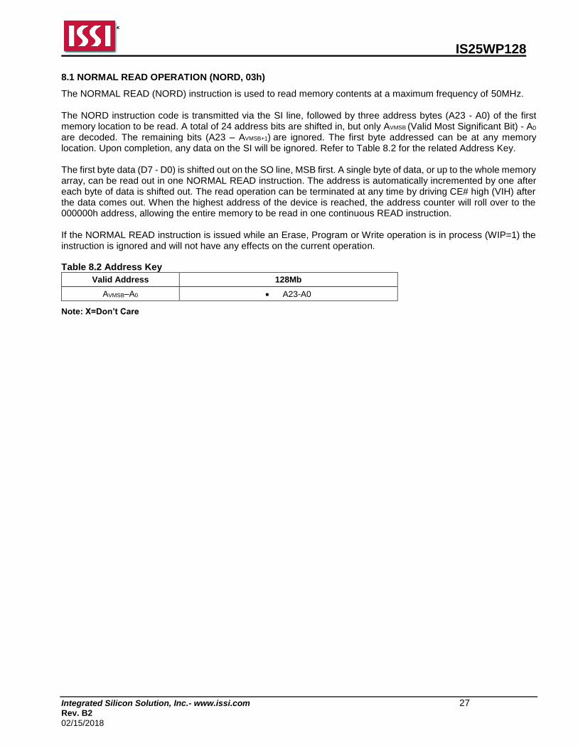
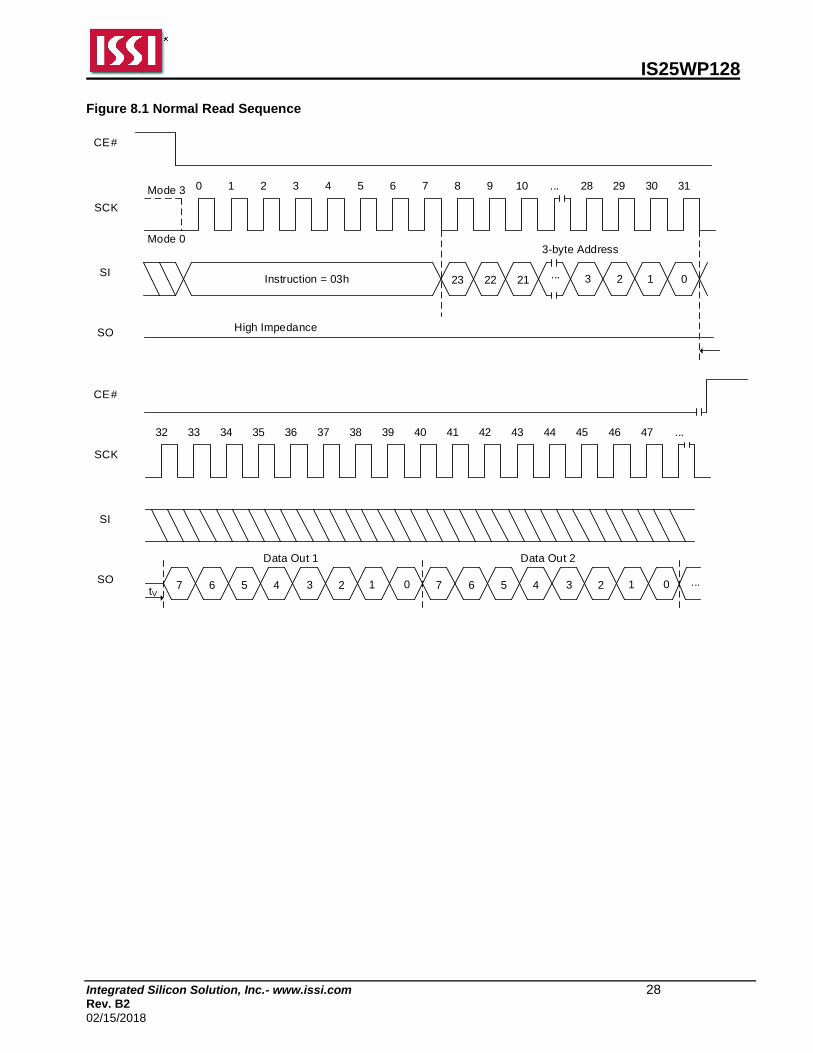
8.1 NORMAL READ OPERATION (NORD, 03h)
The NORMAL READ (NORD) instruction is used to read memory contents at a maximum frequency of 50MHz. The NORD instruction code is transmitted via the SI line, followed by three address bytes (A23 - A0) of the first memory location to be read. A total of 24 address bits are shifted in, but only AVMSB (Valid Most Significant Bit) - A0 are decoded. The remaining bits (A23 – AVMSB+1) are ignored. The first byte addressed can be at any memory location. Upon completion, any data on the SI will be ignored. Refer to Table 8.2 for the related Address Key. The first byte data (D7 - D0) is shifted out on the SO line, MSB first. A single byte of data, or up to the whole memory array, can be read out in one NORMAL READ instruction. The address is automatically incremented by one after each byte of data is shifted out. The read operation can be terminated at any time by driving CE# high (VIH) after the data comes out. When the highest address of the device is reached, the address counter will roll over to the 000000h address, allowing the entire memory to be read in one continuous READ instruction. If the NORMAL READ instruction is issued while an Erase, Program or Write operation is in process (WIP=1) the instruction is ignored and will not have any effects on the current operation.
Table 8.2 Address Key
Valid Address 128Mb
AVMSB–A0 A23-A0
Note: X=Don’t Care
IS25WP128
Integrated Silicon Solution, Inc.- www.issi.com 28 Rev. B2
02/15/2018
Figure 8.1 Normal Read Sequence
7 6
CE#
SCK
SI
5 3 2SO
4 1 0
Data Out 1
Instruction = 03h 23
CE#
SCK
SI3 2
SO
1 0
3-byte Address
High Impedance
22 21 ...
0 1 2 3 4 5 6 7 8 9 10 ... 28 29 30 31
32 33 34 35 36 37 38 39 40 41 42 43 44 45 46 47
Mode 3
Mode 0
...
7 6 5 3 24 1 0tV
Data Out 2
...
IS25WP128
Integrated Silicon Solution, Inc.- www.issi.com 29 Rev. B2
02/15/2018
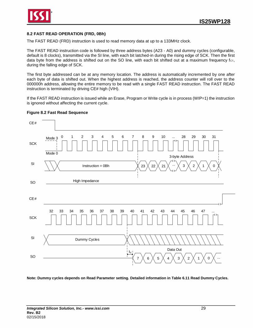
8.2 FAST READ OPERATION (FRD, 0Bh)
The FAST READ (FRD) instruction is used to read memory data at up to a 133MHz clock. The FAST READ instruction code is followed by three address bytes (A23 - A0) and dummy cycles (configurable, default is 8 clocks), transmitted via the SI line, with each bit latched-in during the rising edge of SCK. Then the first data byte from the address is shifted out on the SO line, with each bit shifted out at a maximum frequency fCT, during the falling edge of SCK. The first byte addressed can be at any memory location. The address is automatically incremented by one after each byte of data is shifted out. When the highest address is reached, the address counter will roll over to the 000000h address, allowing the entire memory to be read with a single FAST READ instruction. The FAST READ instruction is terminated by driving CE# high (VIH). If the FAST READ instruction is issued while an Erase, Program or Write cycle is in process (WIP=1) the instruction is ignored without affecting the current cycle. Figure 8.2 Fast Read Sequence
Instruction = 0Bh
3-byte Address
28 29 30 31
32 33 34 35 36 37 38 39 40 41 42 43 44 45 46 47 ...
7 6
CE#
SCK
SI
5 3 2SO
4 1
Data Out
23
CE#
SCK
SI3 2
SO
1 0
High Impedance
22 21 ...
0 1 2 3 4 5 6 7 8 9 10 ...Mode 3
Mode 0
tV
Dummy Cycles
0 ...
Note: Dummy cycles depends on Read Parameter setting. Detailed information in Table 6.11 Read Dummy Cycles.
IS25WP128
Integrated Silicon Solution, Inc.- www.issi.com 30 Rev. B2
02/15/2018
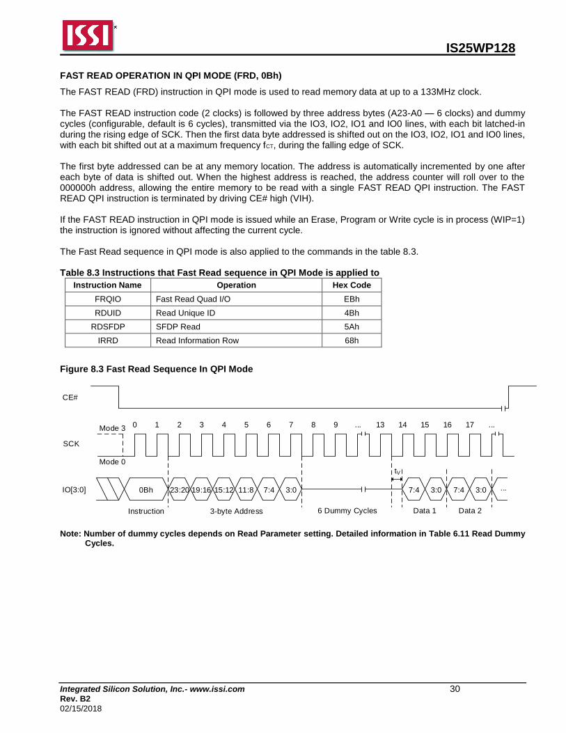
FAST READ OPERATION IN QPI MODE (FRD, 0Bh)
The FAST READ (FRD) instruction in QPI mode is used to read memory data at up to a 133MHz clock. The FAST READ instruction code (2 clocks) is followed by three address bytes (A23-A0 — 6 clocks) and dummy cycles (configurable, default is 6 cycles), transmitted via the IO3, IO2, IO1 and IO0 lines, with each bit latched-in during the rising edge of SCK. Then the first data byte addressed is shifted out on the IO3, IO2, IO1 and IO0 lines, with each bit shifted out at a maximum frequency fCT, during the falling edge of SCK. The first byte addressed can be at any memory location. The address is automatically incremented by one after each byte of data is shifted out. When the highest address is reached, the address counter will roll over to the 000000h address, allowing the entire memory to be read with a single FAST READ QPI instruction. The FAST READ QPI instruction is terminated by driving CE# high (VIH). If the FAST READ instruction in QPI mode is issued while an Erase, Program or Write cycle is in process (WIP=1) the instruction is ignored without affecting the current cycle. The Fast Read sequence in QPI mode is also applied to the commands in the table 8.3. Table 8.3 Instructions that Fast Read sequence in QPI Mode is applied to
Instruction Name Operation Hex Code
FRQIO Fast Read Quad I/O EBh
RDUID Read Unique ID 4Bh
RDSFDP SFDP Read 5Ah
IRRD Read Information Row 68h
Figure 8.3 Fast Read Sequence In QPI Mode
0Bh
CE#
SCK
IO[3:0]
6 Dummy Cycles3-byte Address
0 1 2 3 4 5 6 7 8 9 ... 13 14 15 16 17Mode 3
Mode 0
23:20 7:4 3:0 7:4 3:0
Data 1 Data 2
19:16 15:12 11:8 7:4 3:0
...
tV
...
Instruction
Note: Number of dummy cycles depends on Read Parameter setting. Detailed information in Table 6.11 Read Dummy
Cycles.
IS25WP128
Integrated Silicon Solution, Inc.- www.issi.com 31 Rev. B2
02/15/2018
8.3 HOLD OPERATION
HOLD# is used in conjunction with CE# to select the device. When the device is selected and a serial sequence is underway, HOLD# can be used to pause the serial communication with the master device without resetting the serial sequence. To pause, HOLD# is brought low while the SCK signal is low. To resume serial communication, HOLD# is brought high while the SCK signal is low (SCK may still toggle during HOLD). Inputs to SI will be ignored while SO is in the high impedance state, during HOLD.
Note: HOLD is not supported in DTR mode or with QE=1 or when RESET# is selected for the HOLD# or RESET# pin.
Timing graph can be referenced in AC Parameters Figure 9.4
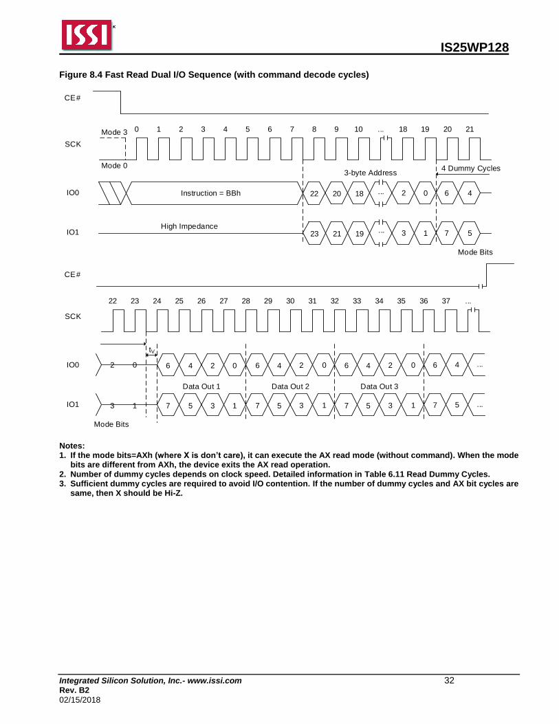
8.4 FAST READ DUAL I/O OPERATION (FRDIO, BBh)
The FRDIO allows the address bits to be input two bits at a time. This may allow for code to be executed directly from the SPI in some applications. The FRDIO instruction code is followed by three address bytes (A23 – A0) and dummy cycles (configurable, default is 4 clocks), transmitted via the IO1 and IO0 lines, with each pair of bits latched-in during the rising edge of SCK. The address MSB is input on IO1, the next bit on IO0, and this shift pattern continues to alternate between the two lines. Depending on the usage of AX read operation mode, a mode byte may be located after address input. The first data byte addressed is shifted out on the IO1 and IO0 lines, with each pair of bits shifted out at a maximum frequency fCT, during the falling edge of SCK. The MSB is output on IO1, while simultaneously the second bit is output on IO0. Figure 8.4 illustrates the timing sequence. The first byte addressed can be at any memory location. The address is automatically incremented by one after each byte of data is shifted out. When the highest address is reached, the address counter will roll over to the 000000h address, allowing the entire memory to be read with a single FRDIO instruction. FRDIO instruction is terminated by driving CE# high (VIH). The device supports the AX read operation by applying mode bits during dummy period. Mode bits consist of 8 bits, such as M7 to M0. Four cycles after address input are reserved for Mode bits in FRDIO execution. M7 to M4 are important for enabling this mode. M3 to M0 become don’t care for future use. When M[7:4]=1010(Ah), it enables the AX read operation and subsequent FRDIO execution skips command code. It saves cycles as described in Figure 8.5. When the code is different from AXh (where X is don’t care), the device exits the AX read operation. After finishing the read operation, device becomes ready to receive a new command. SPI or QPI mode configuration retains the prior setting. Mode bit must be applied during dummy cycles. Number of dummy cycles in Table 6.11 includes number of mode bit cycles. If dummy cycles are configured as 4 cycles, data output will start right after mode bit is applied. If the FRDIO instruction is issued while an Erase, Program or Write cycle is in process (WIP=1) the instruction is ignored and will not affect the current cycle.
IS25WP128
Integrated Silicon Solution, Inc.- www.issi.com 32 Rev. B2
02/15/2018
Figure 8.4 Fast Read Dual I/O Sequence (with command decode cycles)
7 5 3 7 51 3 1
Data Out 1
Instruction = BBh 22
CE#
SCK
2 0 6 4
3-byte Address
High Impedance
20 18 ...
0 1 2 3 4 5 6 7 8 9 10 ... 18 19 20 21
22 23 24 25 26 27 28 29 30 31 32 33 34 35 36 37
Mode 3
Mode 0
...
tV
23 3 1 7 521 19 ...
IO0
IO1
3 1
2 0 6 4 2 6 40 2 0
4 Dummy Cycles
7 5 3 1
6 4 2 0
7 5 ...
6 4 ...
CE#
SCK
IO0
IO1
Data Out 2 Data Out 3
Mode Bits
Mode Bits Notes: 1. If the mode bits=AXh (where X is don’t care), it can execute the AX read mode (without command). When the mode
bits are different from AXh, the device exits the AX read operation. 2. Number of dummy cycles depends on clock speed. Detailed information in Table 6.11 Read Dummy Cycles. 3. Sufficient dummy cycles are required to avoid I/O contention. If the number of dummy cycles and AX bit cycles are
same, then X should be Hi-Z.
IS25WP128
Integrated Silicon Solution, Inc.- www.issi.com 33 Rev. B2
02/15/2018
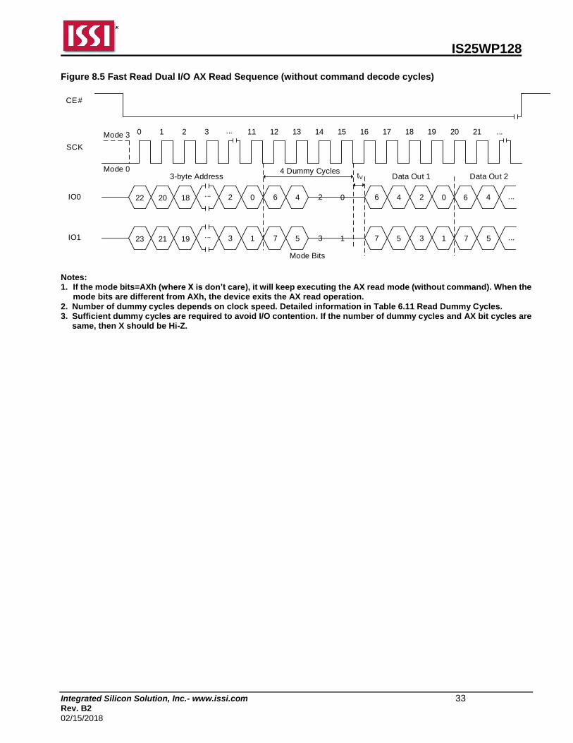
Figure 8.5 Fast Read Dual I/O AX Read Sequence (without command decode cycles)
22
CE#
SCK
2 0
3-byte Address
20 18 ...
0 1 2 3 ... 11 12 13 14 15 16 17 18 19 20 21Mode 3
Mode 0
23 3 121 19 ...
IO0
IO1
4 Dummy Cycles
6
7
6 4
7 5
2 0
3 1
Data Out 1tV
6 4
7 5
2 0
3 1
4
5
Mode Bits
...
...
Data Out 2
...
Notes: 1. If the mode bits=AXh (where X is don’t care), it will keep executing the AX read mode (without command). When the
mode bits are different from AXh, the device exits the AX read operation. 2. Number of dummy cycles depends on clock speed. Detailed information in Table 6.11 Read Dummy Cycles. 3. Sufficient dummy cycles are required to avoid I/O contention. If the number of dummy cycles and AX bit cycles are
same, then X should be Hi-Z.
IS25WP128
Integrated Silicon Solution, Inc.- www.issi.com 34 Rev. B2
02/15/2018
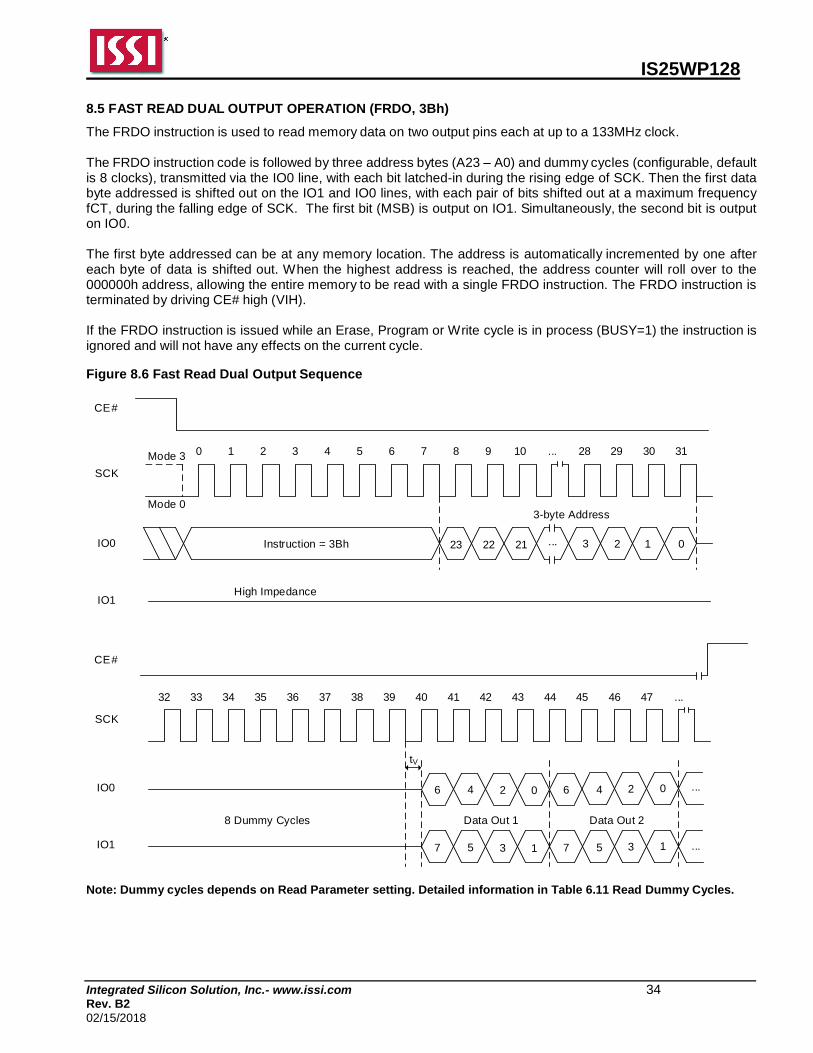
8.5 FAST READ DUAL OUTPUT OPERATION (FRDO, 3Bh)
The FRDO instruction is used to read memory data on two output pins each at up to a 133MHz clock. The FRDO instruction code is followed by three address bytes (A23 – A0) and dummy cycles (configurable, default is 8 clocks), transmitted via the IO0 line, with each bit latched-in during the rising edge of SCK. Then the first data byte addressed is shifted out on the IO1 and IO0 lines, with each pair of bits shifted out at a maximum frequency fCT, during the falling edge of SCK. The first bit (MSB) is output on IO1. Simultaneously, the second bit is output on IO0. The first byte addressed can be at any memory location. The address is automatically incremented by one after each byte of data is shifted out. When the highest address is reached, the address counter will roll over to the 000000h address, allowing the entire memory to be read with a single FRDO instruction. The FRDO instruction is terminated by driving CE# high (VIH). If the FRDO instruction is issued while an Erase, Program or Write cycle is in process (BUSY=1) the instruction is ignored and will not have any effects on the current cycle. Figure 8.6 Fast Read Dual Output Sequence
CE#
SCK
7 5
Data Out 1
Instruction = 3Bh 23
CE#
SCK
3 2 1 0
3-byte Address
High Impedance
22 21 ...
0 1 2 3 4 5 6 7 8 9 10 ... 28 29 30 31
32 33 34 35 36 37 38 39 40 41 42 43 44 45 46 47
Mode 3
Mode 0
...
tV
IO0
IO1
6 4
3 1 7 5
2 0 6 4
3 1 ...
2 0 ...
Data Out 2
IO0
IO1
8 Dummy Cycles
Note: Dummy cycles depends on Read Parameter setting. Detailed information in Table 6.11 Read Dummy Cycles.
IS25WP128
Integrated Silicon Solution, Inc.- www.issi.com 35 Rev. B2
02/15/2018
8.6 FAST READ QUAD OUTPUT OPERATION (FRQO, 6Bh)
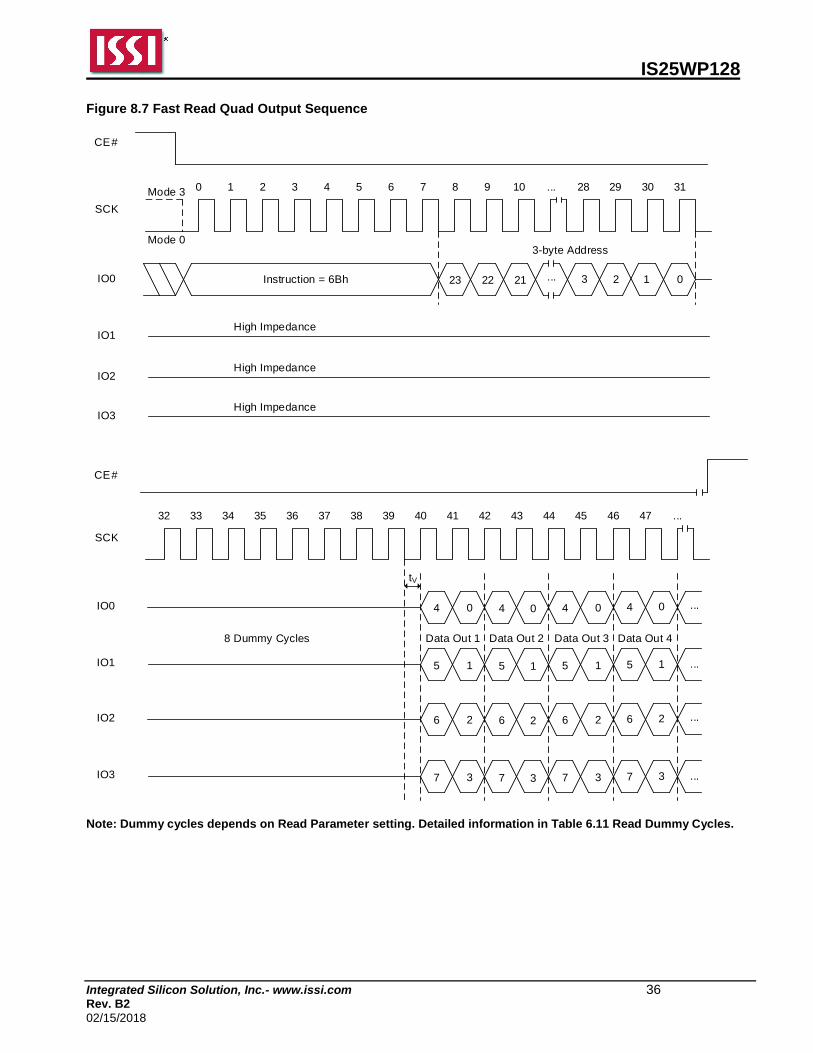
The FRQO instruction is used to read memory data on four output pins each at up to a 133 MHz clock. The FRQO instruction code is followed by three address bytes (A23 – A0) and dummy cycles (configurable, default is 8 clocks), transmitted via the IO0 line, with each bit latched-in during the rising edge of SCK. Then the first data byte addressed is shifted out on the IO3, IO2, IO1 and IO0 lines, with each group of four bits shifted out at a maximum frequency fCT, during the falling edge of SCK. The fi rst bit (MSB) is output on IO3, while simultaneously the second bit is output on IO2, the third bit is output on IO1, etc. The first byte addressed can be at any memory location. The address is automatically incremented after each byte of data is shifted out. When the highest address is reached, the address counter will roll over to the 000000h address, allowing the entire memory to be read with a single FRQO instruction. FRQO instruction is terminated by driving CE# high (VIH). If a FRQO instruction is issued while an Erase, Program or Write cycle is in process (BUSY=1) the instruction is ignored and will not have any effects on the current cycle.
IS25WP128
Integrated Silicon Solution, Inc.- www.issi.com 36 Rev. B2
02/15/2018
Figure 8.7 Fast Read Quad Output Sequence
CE#
SCK
5 1
Data Out 1
Instruction = 6Bh 23
CE#
SCK
3 2 1 0
3-byte Address
High Impedance
22 21 ...
0 1 2 3 4 5 6 7 8 9 10 ... 28 29 30 31
32 33 34 35 36 37 38 39 40 41 42 43 44 45 46 47
Mode 3
Mode 0
...
tV
IO0
IO1
4 0
5 1 5 1
4 0 4 0
5 1 ...
4 0 ...IO0
IO1
8 Dummy Cycles
High ImpedanceIO2
High ImpedanceIO3
7 3
6 2
7 3 7 3
6 2 6 2
7 3 ...
6 2 ...IO2
IO3
Data Out 2 Data Out 3 Data Out 4
Note: Dummy cycles depends on Read Parameter setting. Detailed information in Table 6.11 Read Dummy Cycles.
IS25WP128
Integrated Silicon Solution, Inc.- www.issi.com 37 Rev. B2
02/15/2018
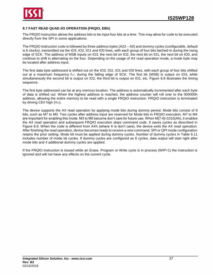
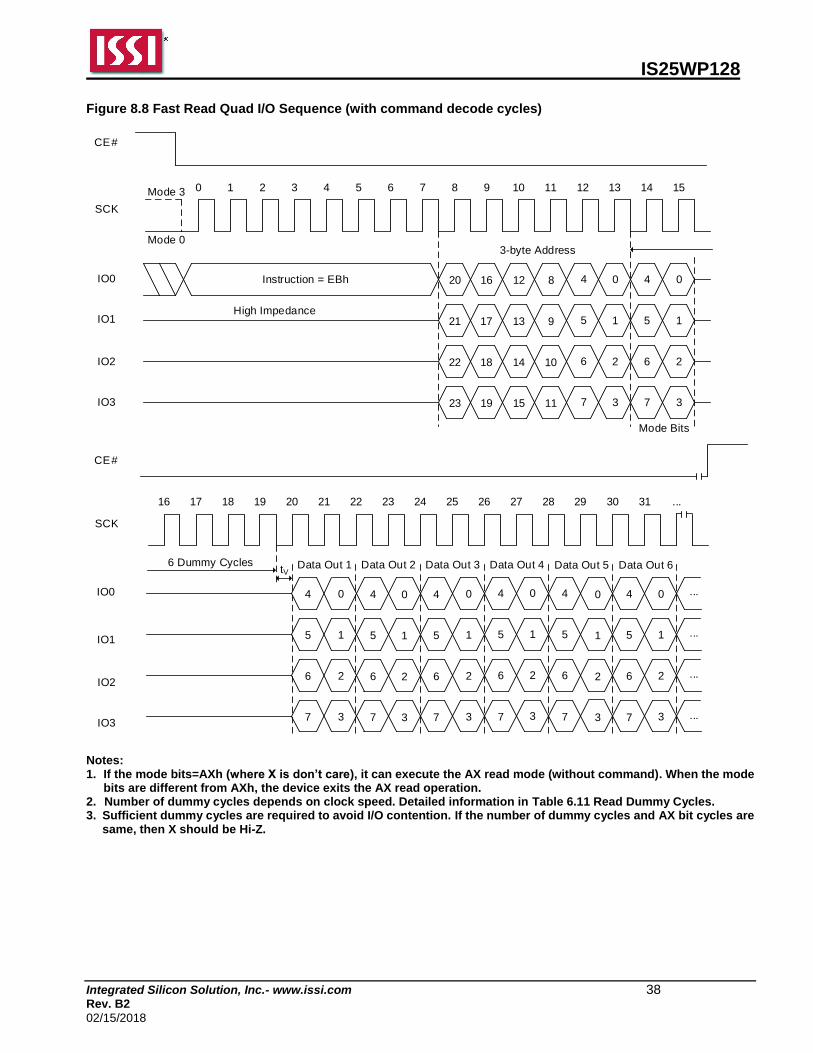
8.7 FAST READ QUAD I/O OPERATION (FRQIO, EBh)
The FRQIO instruction allows the address bits to be input four bits at a time. This may allow for code to be executed directly from the SPI in some applications. The FRQIO instruction code is followed by three address bytes (A23 – A0) and dummy cycles (configurable, default is 6 clocks), transmitted via the IO3, IO2, IO1 and IO0 lines, with each group of four bits latched-in during the rising edge of SCK. The address of MSB inputs on IO3, the next bit on IO2, the next bit on IO1, the next bit on IO0, and continue to shift in alternating on the four. Depending on the usage of AX read operation mode, a mode byte may be located after address input. The first data byte addressed is shifted out on the IO3, IO2, IO1 and IO0 lines, with each group of four bits shifted out at a maximum frequency fCT, during the falling edge of SCK. The first bit (MSB) is output on IO3, while simultaneously the second bit is output on IO2, the third bit is output on IO1, etc. Figure 8.8 illustrates the timing sequence. The first byte addressed can be at any memory location. The address is automatically incremented after each byte of data is shifted out. When the highest address is reached, the address counter will roll over to the 000000h address, allowing the entire memory to be read with a single FRQIO instruction. FRQIO instruction is terminated by driving CE# high (VIH). The device supports the AX read operation by applying mode bits during dummy period. Mode bits consist of 8 bits, such as M7 to M0. Two cycles after address input are reserved for Mode bits in FRQIO execution. M7 to M4 are important for enabling this mode. M3 to M0 become don’t care for future use. When M[7:4]=1010(Ah), it enables the AX read operation and subsequent FRQIO execution skips command code. It saves cycles as described in Figure 8.9. When the code is different from AXh (where X is don’t care), the device exits the AX read operation. After finishing the read operation, device becomes ready to receive a new command. SPI or QPI mode configuration retains the prior setting. Mode bit must be applied during dummy cycles. Number of dummy cycles in Table 6.11 includes number of mode bit cycles. If dummy cycles are configured as 6 cycles, data output will start right after mode bits and 4 additional dummy cycles are applied. If the FRQIO instruction is issued while an Erase, Program or Write cycle is in process (WIP=1) the instruction is ignored and will not have any effects on the current cycle.
IS25WP128
Integrated Silicon Solution, Inc.- www.issi.com 38 Rev. B2
02/15/2018
Figure 8.8 Fast Read Quad I/O Sequence (with command decode cycles)
CE#
SCK
5 1
Data Out 1
Instruction = EBh 20
CE#
SCK
4 0 4 0
3-byte Address
High Impedance
16 12 8
0 1 2 3 4 5 6 7 8 9 10 11 12 13 14 15
16 17 18 19 20 21 22 23 24 25 26 27 28 29 30 31
Mode 3
Mode 0
...
tV
IO0
IO1
4 0
5 1 5 1
4 0 4 0
5 1
4 0IO0
IO1
21 5 1 5 117 13 9
22 6 2 6 218 14 10
23 7 3 7 319 15 11
Mode Bits
IO2
IO3
6 2 6 2 6 2 6 2
7 3 7 3 7 3 7 3
Data Out 2 Data Out 3 Data Out 4
IO2
IO3
1
0
5 1 ...
4 0 ...
2 6 2 ...
3 7 3 ...
5
4
6
7
6 Dummy Cycles Data Out 5 Data Out 6
Notes: 1. If the mode bits=AXh (where X is don’t care), it can execute the AX read mode (without command). When the mode
bits are different from AXh, the device exits the AX read operation. 2. Number of dummy cycles depends on clock speed. Detailed information in Table 6.11 Read Dummy Cycles. 3. Sufficient dummy cycles are required to avoid I/O contention. If the number of dummy cycles and AX bit cycles are
same, then X should be Hi-Z.
IS25WP128
Integrated Silicon Solution, Inc.- www.issi.com 39 Rev. B2
02/15/2018
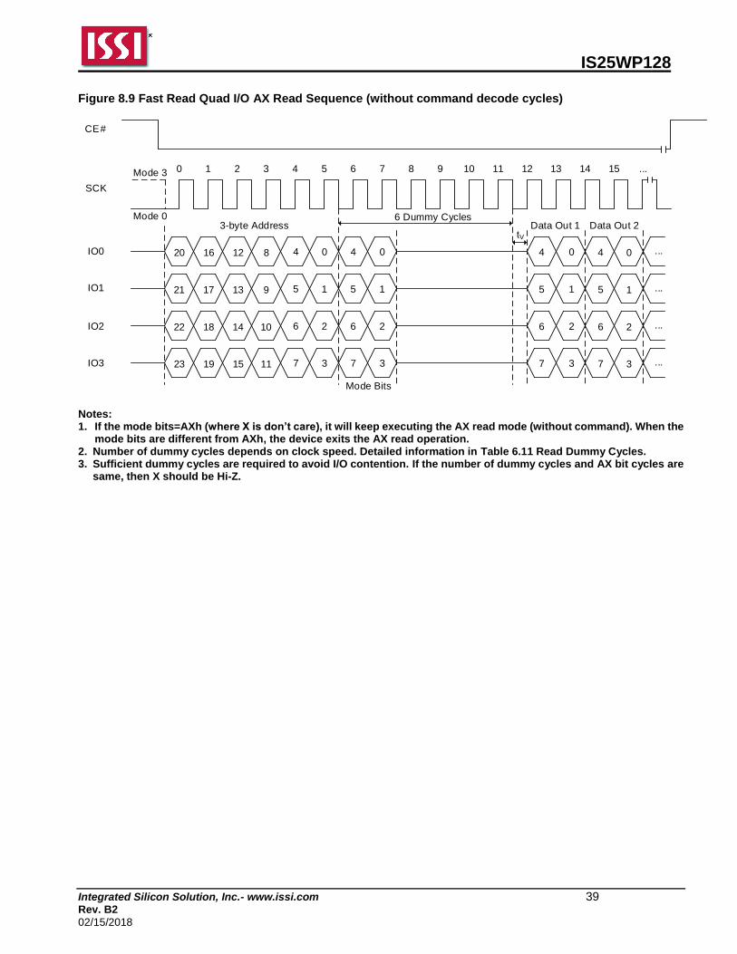
Figure 8.9 Fast Read Quad I/O AX Read Sequence (without command decode cycles)
20
CE#
SCK
4 0 4 0
3-byte Address
16 12 8
0 1 2 3 4 5 6 7 8 9 10 11 12 13 14 15Mode 3
Mode 0
IO0
IO1 21 5 1 5 117 13 9
22 6 2 6 218 14 10
23 7 3 7 319 15 11
Mode Bits
IO2
IO3
5 1
4 0
5 1
4 0
6 2 6 2
7 3 7 3
...
...
...
...
Data Out 1 Data Out 2
...
tV
6 Dummy Cycles
Notes: 1. If the mode bits=AXh (where X is don’t care), it will keep executing the AX read mode (without command). When the
mode bits are different from AXh, the device exits the AX read operation. 2. Number of dummy cycles depends on clock speed. Detailed information in Table 6.11 Read Dummy Cycles. 3. Sufficient dummy cycles are required to avoid I/O contention. If the number of dummy cycles and AX bit cycles are
same, then X should be Hi-Z.
IS25WP128
Integrated Silicon Solution, Inc.- www.issi.com 40 Rev. B2
02/15/2018
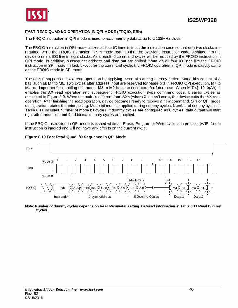
FAST READ QUAD I/O OPERATION IN QPI MODE (FRQIO, EBh)
The FRQIO instruction in QPI mode is used to read memory data at up to a 133MHz clock. The FRQIO instruction in QPI mode utilizes all four IO lines to input the instruction code so that only two clocks are required, while the FRQIO instruction in SPI mode requires that the byte-long instruction code is shifted into the device only via IO0 line in eight clocks. As a result, 6 command cycles will be reduced by the FRQIO instruction in QPI mode. In addition, subsequent address and data out are shifted in/out via all four IO lines like the FRQIO instruction in SPI mode. In fact, except for the command cycle, the FRQIO operation in QPI mode is exactly same as the FRQIO mode in SPI mode. The device supports the AX read operation by applying mode bits during dummy period. Mode bits consist of 8 bits, such as M7 to M0. Two cycles after address input are reserved for Mode bits in FRQIO QPI execution. M7 to M4 are important for enabling this mode. M3 to M0 become don’t care for future use. When M[7:4]=1010(Ah), it enables the AX read operation and subsequent FRQIO execution skips command code. It saves cycles as described in Figure 8.9. When the code is different from AXh (where X is don’t care), the device exits the AX read operation. After finishing the read operation, device becomes ready to receive a new command. SPI or QPI mode configuration retains the prior setting. Mode bit must be applied during dummy cycles. Number of dummy cycles in Table 6.11 includes number of mode bit cycles. If dummy cycles are configured as 6 cycles, data output will start right after mode bits and 4 additional dummy cycles are applied. If the FRQIO instruction in QPI mode is issued while an Erase, Program or Write cycle is in process (WIP=1) the instruction is ignored and will not have any effects on the current cycle. Figure 8.10 Fast Read Quad I/O Sequence In QPI Mode
EBh
CE#
SCK
IO[3:0]
6 Dummy Cycles3-byte Address
0 1 2 3 4 5 6 7 8 9
...
13 14 15 16 17Mode 3
Mode 0
23:20 7:4 3:0 7:4 3:0
Data 1 Data 2
19:16 15:12 11:8 7:4 3:0
...
tV
Instruction
Mode Bits
7:4 3:0
...
Note: Number of dummy cycles depends on Read Parameter setting. Detailed information in Table 6.11 Read Dummy
Cycles.
IS25WP128
Integrated Silicon Solution, Inc.- www.issi.com 41 Rev. B2
02/15/2018
8.8 PAGE PROGRAM OPERATION (PP, 02h)
The Page Program (PP) instruction allows up to 256 bytes data to be programmed into memory in a single operation. The destination of the memory to be programmed must be outside the protected memory area set by the Block Protection (TBS, BP3, BP2, BP1, BP0) bits. A PP instruction which attempts to program into a page that is write-protected will be ignored. Before the execution of PP instruction, the Write Enable Latch (WEL) must be enabled through a Write Enable (WREN) instruction. The PP instruction code, three address bytes and program data (1 to 256 bytes) are input via the SI line. Program operation will start immediately after the CE# is brought high, otherwise the PP instruction will not be executed. The internal control logic automatically handles the programming voltages and timing.The progress or completion of the program operation can be determined by reading the WIP bit in Status Register via a RDSR instruction. If the WIP bit is “1”, the program operation is still in progress. If WIP bit is “0”, the program operation has completed. If more than 256 bytes data are sent to a device, the address counter rolls over within the same page, the previously latched data are discarded, and the last 256 bytes are kept to be programmed into the page. The starting byte can be anywhere within the page. When the end of the page is reached, the address will wrap around to the beginning of the same page. If the data to be programmed are less than a full page, the data of all other bytes on the same page will remain unchanged.
Note: A program operation can alter “1”s into “0”s, but an erase operation is required to change “0”s back to “1”s. A byte cannot be reprogrammed without first erasing the whole sector or block.
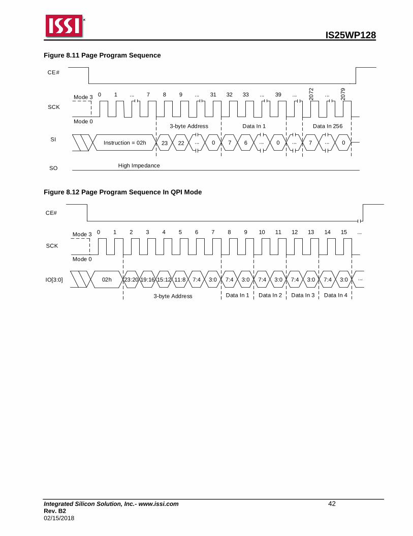
IS25WP128
Integrated Silicon Solution, Inc.- www.issi.com 42 Rev. B2
02/15/2018
Figure 8.11 Page Program Sequence
Instruction = 02h 23
CE#
SCK
SI7 6
SO
7
3-byte Address
High Impedance
22 ... 0
Data In 1 Data In 256
0 1 ... 7 8 9 ... 31 32 33 ... 39 ...
20
72
...
20
79
Mode 3
Mode 0
... 0 ... ... 0
Figure 8.12 Page Program Sequence In QPI Mode
02h
CE#
SCK
IO[3:0]
3-byte Address
0 1 2 3 4 5 6 7 8 9 10 11 12 13 14 15Mode 3
Mode 0
23:20 7:4 3:0 7:4 3:0
Data In 1 Data In 2
19:16 15:12 11:8 7:4 3:0 7:4 3:0 7:4 3:0
Data In 3 Data In 4
...
...
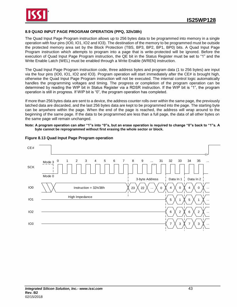
IS25WP128
Integrated Silicon Solution, Inc.- www.issi.com 43 Rev. B2
02/15/2018
8.9 QUAD INPUT PAGE PROGRAM OPERATION (PPQ, 32h/38h)
The Quad Input Page Program instruction allows up to 256 bytes data to be programmed into memory in a single operation with four pins (IO0, IO1, IO2 and IO3). The destination of the memory to be programmed must be outside the protected memory area set by the Block Protection (TBS, BP3, BP2, BP1, BP0) bits. A Quad Input Page Program instruction which attempts to program into a page that is write-protected will be ignored. Before the execution of Quad Input Page Program instruction, the QE bit in the Status Register must be set to “1” and the Write Enable Latch (WEL) must be enabled through a Write Enable (WREN) instruction. The Quad Input Page Program instruction code, three address bytes and program data (1 to 256 bytes) are input via the four pins (IO0, IO1, IO2 and IO3). Program operation will start immediately after the CE# is brought high, otherwise the Quad Input Page Program instruction will not be executed. The internal control logic automatically handles the programming voltages and timing. The progress or completion of the program operation can be determined by reading the WIP bit in Status Register via a RDSR instruction. If the WIP bit is “1”, the program operation is still in progress. If WIP bit is “0”, the program operation has completed. If more than 256 bytes data are sent to a device, the address counter rolls over within the same page, the previously latched data are discarded, and the last 256 bytes data are kept to be programmed into the page. The starting byte can be anywhere within the page. When the end of the page is reached, the address will wrap around to the beginning of the same page. If the data to be programmed are less than a full page, the data of all other bytes on the same page will remain unchanged.
Note: A program operation can alter “1”s into “0”s, but an erase operation is required to change “0”s back to “1”s. A byte cannot be reprogrammed without first erasing the whole sector or block.
Figure 8.13 Quad Input Page Program operation
Instruction = 32h/38h 23
CE#
SCK
4 0 4 0
3-byte Address
High Impedance
22 ... 0
0 1 2 3 4 5 6 7 8 9 31 32 33 34 35Mode 3
Mode 0
IO0
IO1 5 1 5 1
6 2 6 2
7 3 7 3
Data In 2
IO2
IO3
...
Data In 1
...
...
...
...
...
IS25WP128
Integrated Silicon Solution, Inc.- www.issi.com 44 Rev. B2
02/15/2018
8.10 ERASE OPERATION
The memory array of the device is organized into uniform 4 Kbyte sectors or 32/64 Kbyte uniform blocks (a block consists of eight/sixteen adjacent sectors respectively). Before a byte is reprogrammed, the sector or block that contains the byte must be erased (erasing sets bits to “1”). In order to erase the device, there are three erase instructions available: Sector Erase (SER), Block Erase (BER) and Chip Erase (CER). A sector erase operation allows any individual sector to be erased without affecting the data in other sectors. A block erase operation erases any individual block. A chip erase operation erases the whole memory array of a device. A sector erase, block erase, or chip erase operation can be executed prior to any programming operation.
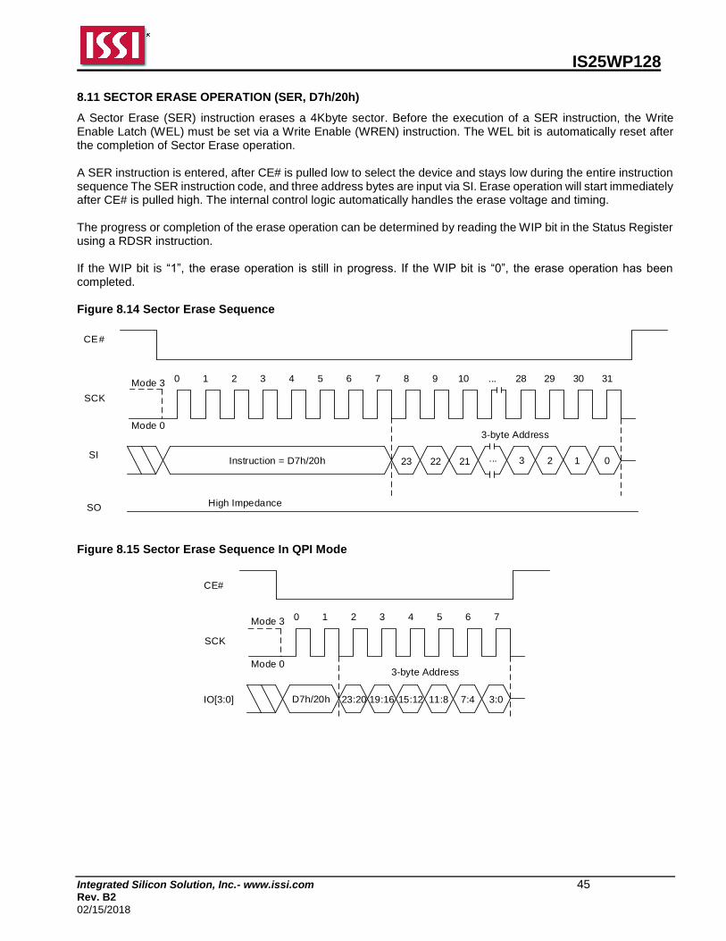
IS25WP128
Integrated Silicon Solution, Inc.- www.issi.com 45 Rev. B2
02/15/2018
8.11 SECTOR ERASE OPERATION (SER, D7h/20h)
A Sector Erase (SER) instruction erases a 4Kbyte sector. Before the execution of a SER instruction, the Write Enable Latch (WEL) must be set via a Write Enable (WREN) instruction. The WEL bit is automatically reset after the completion of Sector Erase operation. A SER instruction is entered, after CE# is pulled low to select the device and stays low during the entire instruction sequence The SER instruction code, and three address bytes are input via SI. Erase operation will start immediately after CE# is pulled high. The internal control logic automatically handles the erase voltage and timing. The progress or completion of the erase operation can be determined by reading the WIP bit in the Status Register using a RDSR instruction. If the WIP bit is “1”, the erase operation is still in progress. If the WIP bit is “0”, the erase operation has been completed. Figure 8.14 Sector Erase Sequence
Instruction = D7h/20h 23
CE#
SCK
SI3 2
SO
1 0
3-byte Address
High Impedance
22 21 ...
0 1 2 3 4 5 6 7 8 9 10 ... 28 29 30 31Mode 3
Mode 0
Figure 8.15 Sector Erase Sequence In QPI Mode
D7h/20h
CE#
SCK
IO[3:0]
3-byte Address
0 1 2 3 4 5 6 7Mode 3
Mode 0
23:20 19:16 15:12 11:8 7:4 3:0
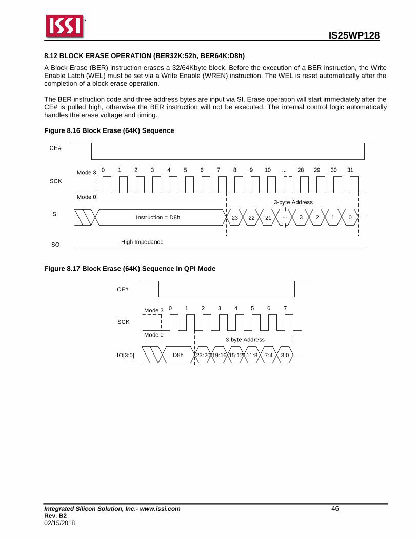
IS25WP128
Integrated Silicon Solution, Inc.- www.issi.com 46 Rev. B2
02/15/2018
8.12 BLOCK ERASE OPERATION (BER32K:52h, BER64K:D8h)
A Block Erase (BER) instruction erases a 32/64Kbyte block. Before the execution of a BER instruction, the Write Enable Latch (WEL) must be set via a Write Enable (WREN) instruction. The WEL is reset automatically after the completion of a block erase operation. The BER instruction code and three address bytes are input via SI. Erase operation will start immediately after the CE# is pulled high, otherwise the BER instruction will not be executed. The internal control logic automatically handles the erase voltage and timing. Figure 8.16 Block Erase (64K) Sequence
Instruction = D8h 23
CE#
SCK
SI3 2
SO
1 0
3-byte Address
High Impedance
22 21 ...
0 1 2 3 4 5 6 7 8 9 10 ... 28 29 30 31Mode 3
Mode 0
Figure 8.17 Block Erase (64K) Sequence In QPI Mode
D8h
CE#
SCK
IO[3:0]
3-byte Address
0 1 2 3 4 5 6 7Mode 3
Mode 0
23:20 19:16 15:12 11:8 7:4 3:0
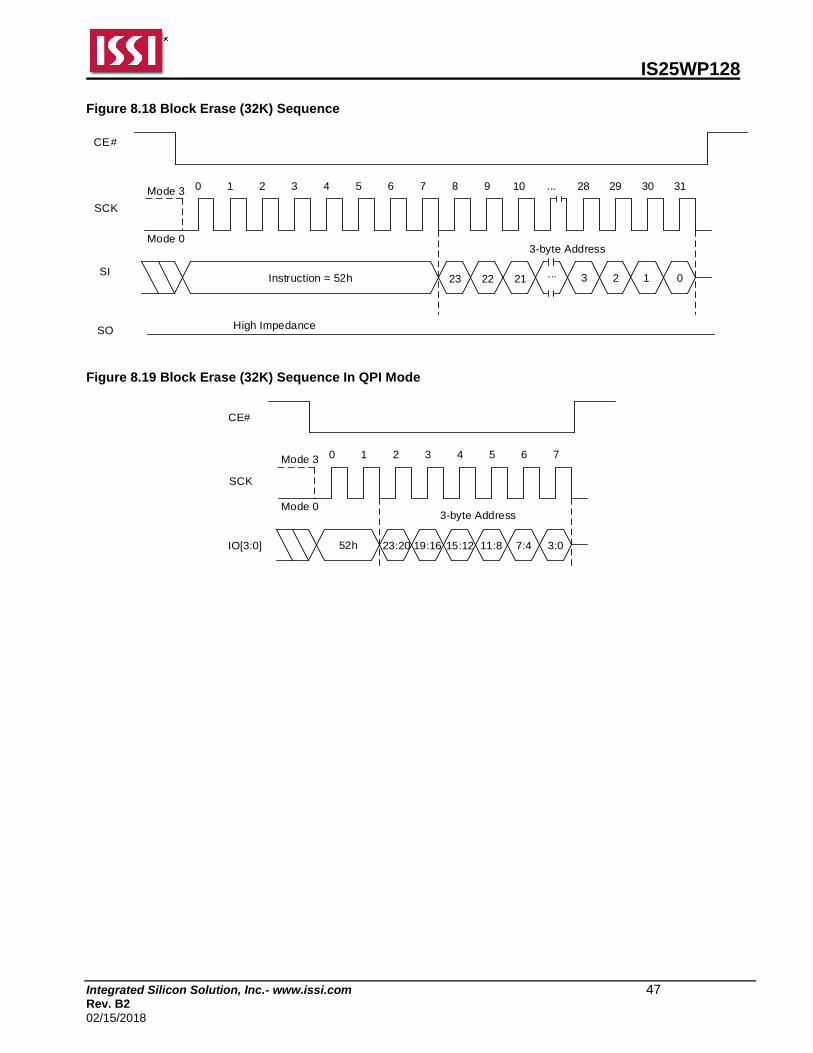
IS25WP128
Integrated Silicon Solution, Inc.- www.issi.com 47 Rev. B2
02/15/2018
Figure 8.18 Block Erase (32K) Sequence
Instruction = 52h 23
CE#
SCK
SI3 2
SO
1 0
3-byte Address
High Impedance
22 21...
0 1 2 3 4 5 6 7 8 9 10 ... 28 29 30 31Mode 3
Mode 0
Figure 8.19 Block Erase (32K) Sequence In QPI Mode
52h
CE#
SCK
IO[3:0]
3-byte Address
0 1 2 3 4 5 6 7Mode 3
Mode 0
23:20 19:16 15:12 11:8 7:4 3:0
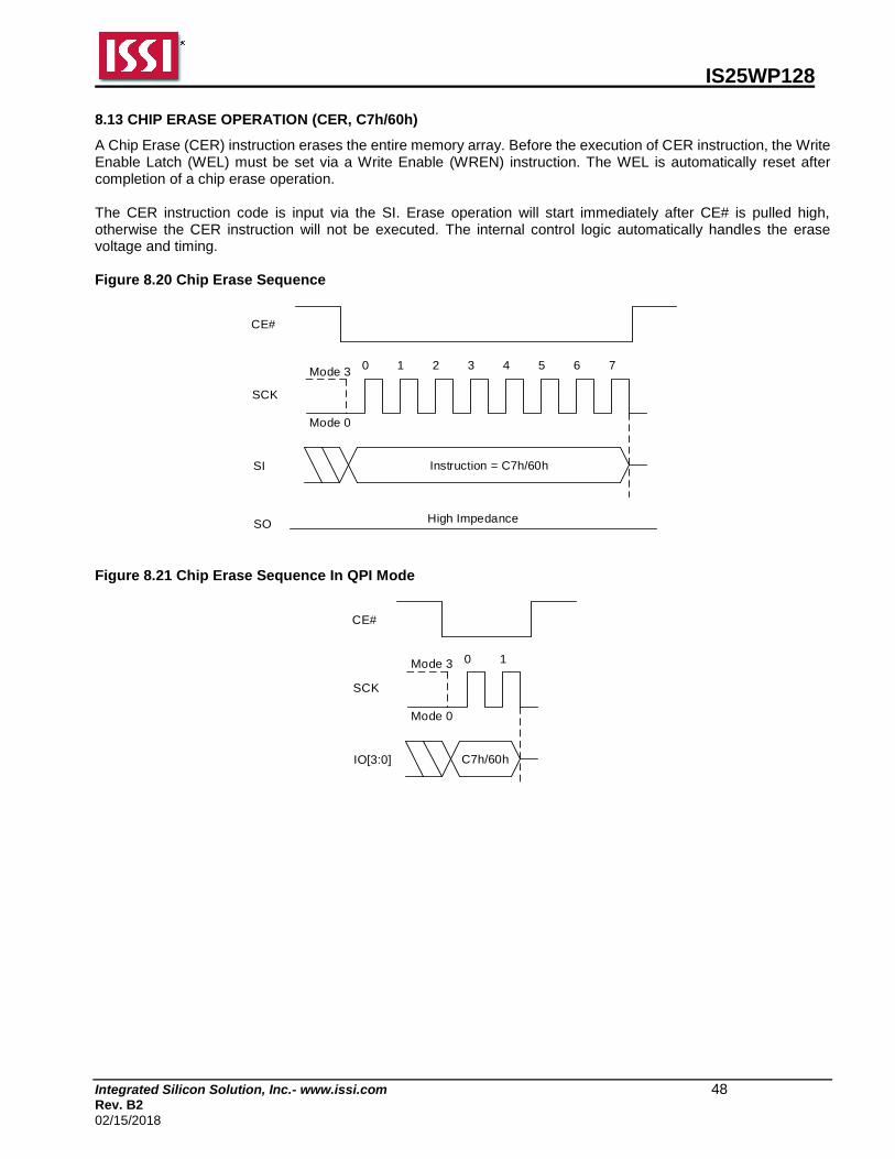
IS25WP128
Integrated Silicon Solution, Inc.- www.issi.com 48 Rev. B2
02/15/2018
8.13 CHIP ERASE OPERATION (CER, C7h/60h)
A Chip Erase (CER) instruction erases the entire memory array. Before the execution of CER instruction, the Write Enable Latch (WEL) must be set via a Write Enable (WREN) instruction. The WEL is automatically reset after completion of a chip erase operation. The CER instruction code is input via the SI. Erase operation will start immediately after CE# is pulled high, otherwise the CER instruction will not be executed. The internal control logic automatically handles the erase voltage and timing. Figure 8.20 Chip Erase Sequence
Instruction = C7h/60h
CE#
SCK
SI
0 1 2 3 4 5 6 7Mode 3
Mode 0
SOHigh Impedance
Figure 8.21 Chip Erase Sequence In QPI Mode
C7h/60h
CE#
SCK
IO[3:0]
0 1Mode 3
Mode 0
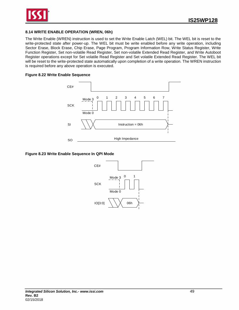
IS25WP128
Integrated Silicon Solution, Inc.- www.issi.com 49 Rev. B2
02/15/2018
8.14 WRITE ENABLE OPERATION (WREN, 06h)
The Write Enable (WREN) instruction is used to set the Write Enable Latch (WEL) bit. The WEL bit is reset to the write-protected state after power-up. The WEL bit must be write enabled before any write operation, including Sector Erase, Block Erase, Chip Erase, Page Program, Program Information Row, Write Status Register, Write Function Register, Set non-volatile Read Register, Set non-volatile Extended Read Register, and Write Autoboot Register operations except for Set volatile Read Register and Set volatile Extended Read Register. The WEL bit will be reset to the write-protected state automatically upon completion of a write operation. The WREN instruction is required before any above operation is executed. Figure 8.22 Write Enable Sequence
Instruction = 06h
CE#
SCK
SI
0 1 2 3 4 5 6 7Mode 3
Mode 0
SOHigh Impedance
Figure 8.23 Write Enable Sequence In QPI Mode
06h
CE#
SCK
IO[3:0]
0 1Mode 3
Mode 0
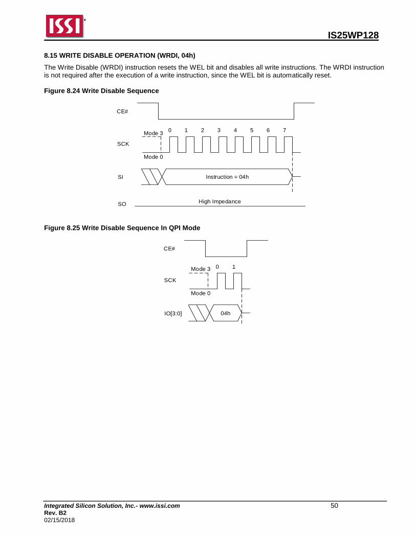
IS25WP128
Integrated Silicon Solution, Inc.- www.issi.com 50 Rev. B2
02/15/2018
8.15 WRITE DISABLE OPERATION (WRDI, 04h)
The Write Disable (WRDI) instruction resets the WEL bit and disables all write instructions. The WRDI instruction is not required after the execution of a write instruction, since the WEL bit is automatically reset. Figure 8.24 Write Disable Sequence
Instruction = 04h
CE#
SCK
SI
0 1 2 3 4 5 6 7Mode 3
Mode 0
SOHigh Impedance
Figure 8.25 Write Disable Sequence In QPI Mode
04h
CE#
SCK
IO[3:0]
0 1Mode 3
Mode 0
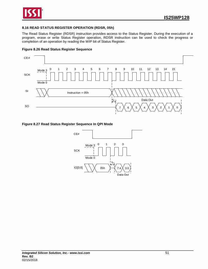
IS25WP128
Integrated Silicon Solution, Inc.- www.issi.com 51 Rev. B2
02/15/2018
8.16 READ STATUS REGISTER OPERATION (RDSR, 05h)
The Read Status Register (RDSR) instruction provides access to the Status Register. During the execution of a program, erase or write Status Register operation, RDSR instruction can be used to check the progress or completion of an operation by reading the WIP bit of Status Register. Figure 8.26 Read Status Register Sequence
Instruction = 05h
7
CE#
SCK
SI
3 2SO 1 0
Data Out
6 5
0 1 2 3 4 5 6 7 8 9 10 11 12 13 14 15Mode 3
Mode 0
4
tV
Figure 8.27 Read Status Register Sequence In QPI Mode
05h
0 1Mode 3
Mode 0
2 3
7:4 3:0
CE#
SCK
IO[3:0]
tV
Data Out
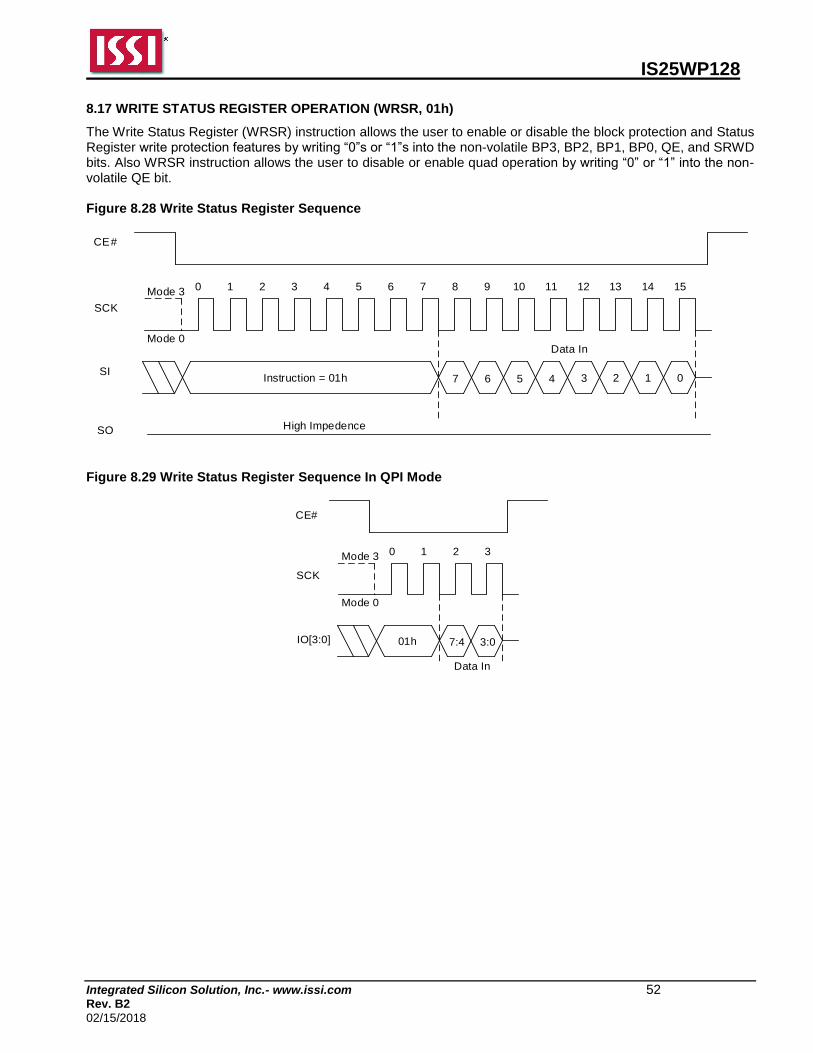
IS25WP128
Integrated Silicon Solution, Inc.- www.issi.com 52 Rev. B2
02/15/2018
8.17 WRITE STATUS REGISTER OPERATION (WRSR, 01h)
The Write Status Register (WRSR) instruction allows the user to enable or disable the block protection and Status Register write protection features by writing “0”s or “1”s into the non-volatile BP3, BP2, BP1, BP0, QE, and SRWD bits. Also WRSR instruction allows the user to disable or enable quad operation by writing “0” or “1” into the non-volatile QE bit. Figure 8.28 Write Status Register Sequence
Instruction = 01h
CE#
SCK
SI
SO
Data In
0 1 2 3 4 5 6 7 8 9 10 11 12 13 14 15Mode 3
Mode 0
7 3 2 1 06 5 4
High Impedence
Figure 8.29 Write Status Register Sequence In QPI Mode
01h
0 1Mode 3
Mode 0
2 3
7:4 3:0
CE#
SCK
IO[3:0]
Data In
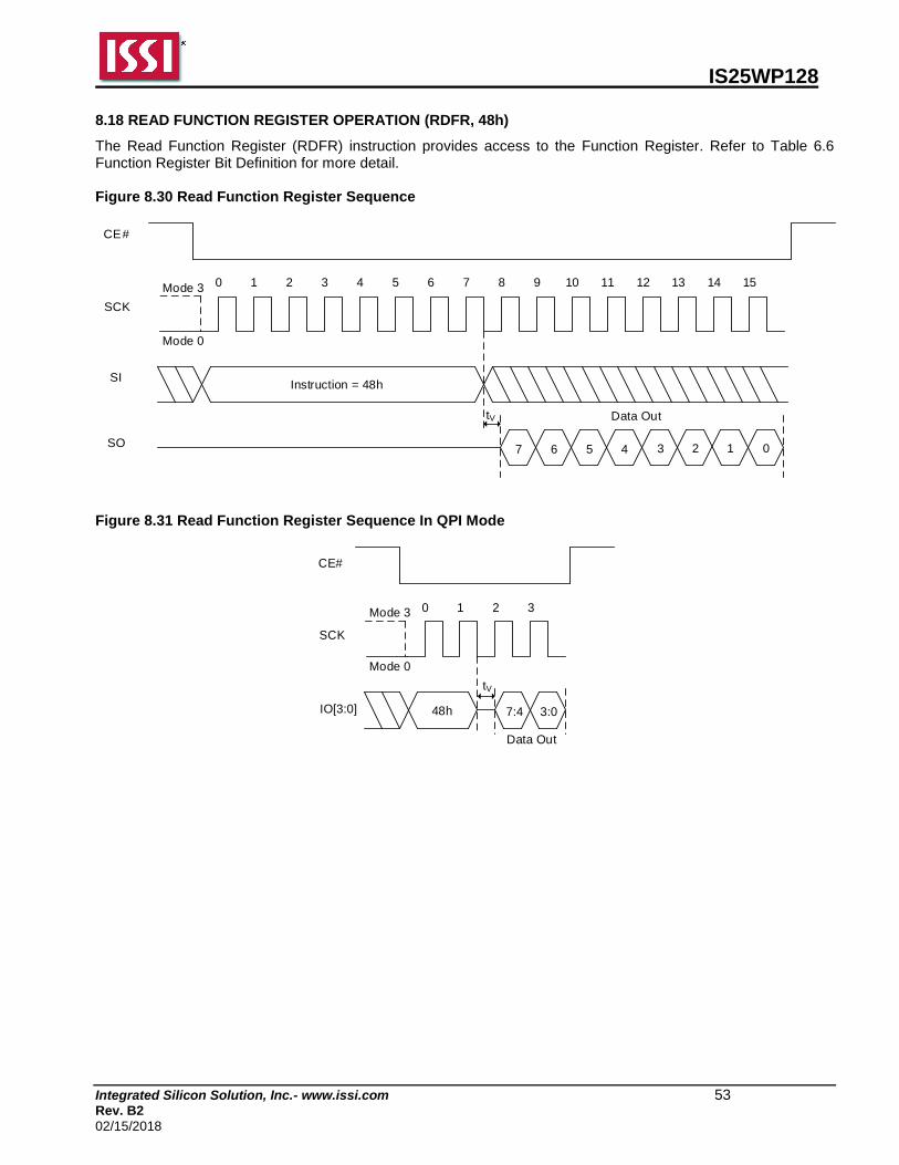
IS25WP128
Integrated Silicon Solution, Inc.- www.issi.com 53 Rev. B2
02/15/2018
8.18 READ FUNCTION REGISTER OPERATION (RDFR, 48h)
The Read Function Register (RDFR) instruction provides access to the Function Register. Refer to Table 6.6 Function Register Bit Definition for more detail. Figure 8.30 Read Function Register Sequence
Instruction = 48h
7
CE#
SCK
SI
3 2SO 1 0
Data Out
6 5
0 1 2 3 4 5 6 7 8 9 10 11 12 13 14 15Mode 3
Mode 0
4
tV
Figure 8.31 Read Function Register Sequence In QPI Mode
48h
0 1Mode 3
Mode 0
2 3
7:4 3:0
CE#
SCK
IO[3:0]
tV
Data Out
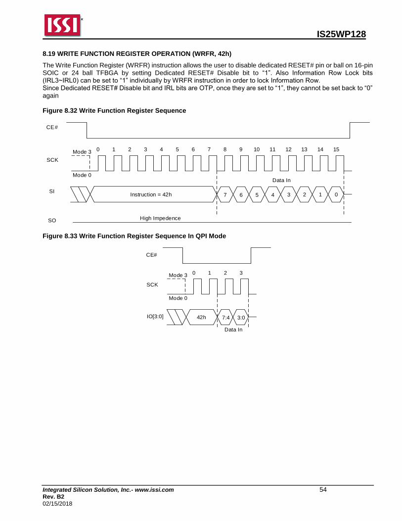
IS25WP128
Integrated Silicon Solution, Inc.- www.issi.com 54 Rev. B2
02/15/2018
8.19 WRITE FUNCTION REGISTER OPERATION (WRFR, 42h)
The Write Function Register (WRFR) instruction allows the user to disable dedicated RESET# pin or ball on 16-pin SOIC or 24 ball TFBGA by setting Dedicated RESET# Disable bit to “1”. Also Information Row Lock bits (IRL3~IRL0) can be set to “1” individually by WRFR instruction in order to lock Information Row. Since Dedicated RESET# Disable bit and IRL bits are OTP, once they are set to “1”, they cannot be set back to “0” again Figure 8.32 Write Function Register Sequence
Instruction = 42h
CE#
SCK
SI
SO
Data In
0 1 2 3 4 5 6 7 8 9 10 11 12 13 14 15Mode 3
Mode 0
7 3 2 1 06 5 4
High Impedence
Figure 8.33 Write Function Register Sequence In QPI Mode
42h
0 1Mode 3
Mode 0
2 3
7:4 3:0
CE#
SCK
IO[3:0]
Data In
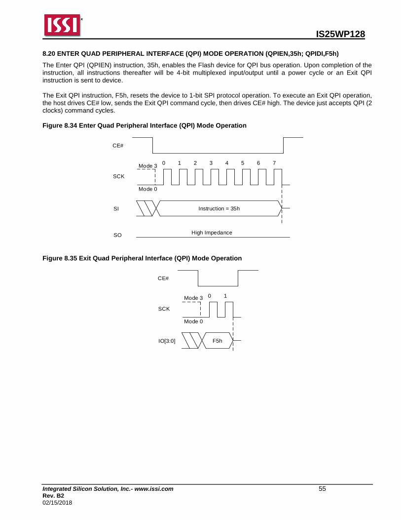
IS25WP128
Integrated Silicon Solution, Inc.- www.issi.com 55 Rev. B2
02/15/2018
8.20 ENTER QUAD PERIPHERAL INTERFACE (QPI) MODE OPERATION (QPIEN,35h; QPIDI,F5h)
The Enter QPI (QPIEN) instruction, 35h, enables the Flash device for QPI bus operation. Upon completion of the instruction, all instructions thereafter will be 4-bit multiplexed input/output until a power cycle or an Exit QPI instruction is sent to device. The Exit QPI instruction, F5h, resets the device to 1-bit SPI protocol operation. To execute an Exit QPI operation, the host drives CE# low, sends the Exit QPI command cycle, then drives CE# high. The device just accepts QPI (2 clocks) command cycles. Figure 8.34 Enter Quad Peripheral Interface (QPI) Mode Operation
Instruction = 35h
CE#
SCK
SI
0 1 2 3 4 5 6 7Mode 3
Mode 0
SOHigh Impedance
Figure 8.35 Exit Quad Peripheral Interface (QPI) Mode Operation
F5h
CE#
SCK
IO[3:0]
0 1Mode 3
Mode 0
IS25WP128
Integrated Silicon Solution, Inc.- www.issi.com 56 Rev. B2
02/15/2018
8.21 PROGRAM/ERASE SUSPEND & RESUME
The device allows the interruption of Sector Erase, Block Erase, or Page Program operations to conduct other operations. 75h/B0h command for suspend and 7Ah/30h for resume will be used. (SPI/QPI all acceptable) Function Register bit2 (PSUS) and bit3 (ESUS) are used to check whether or not the device is in suspend mode. Suspend to read ready timing: 100µs Resume to another suspend timing: 400µs PROGRAM/ERASE SUSPEND DURING SECTOR-ERASE OR BLOCK-ERASE (PERSUS 75h/B0h) The Program/Erase Suspend allows the interruption of Sector Erase and Block Erase operations. After the Program/Erase Suspend, WEL bit will be disabled, therefore only read related, resume and reset commands can be accepted. Refer to Table 8.4 for more detail. To execute the Program/Erase Suspend operation, the host drives CE# low, sends the Program/Erase Suspend command cycle (75h/B0h), then drives CE# high. The Function Register indicates that the erase has been suspended by changing the ESUS bit from “0” to “1”, but the device will not accept another command until it is ready. To determine when the device will accept a new command, poll the WIP bit in the Status Register or wait the specified time tSUS. When ESUS bit is issued, the Write Enable Latch (WEL) bit will be reset. PROGRAM/ERASE SUSPEND DURING PAGE PROGRAMMING (PERSUS 75h/B0h) The Program/Erase Suspend allows the interruption of all array program operations. After the Program/Erase Suspend command, WEL bit will be disabled, therefore only read related, resume and reset command can be accepted. Refer to Table 8.4 for more detail. To execute the Program/Erase Suspend operation, the host drives CE# low, sends the Program/Erase Suspend command cycle (75h/B0h), then drives CE# high. The Function Register indicates that the programming has been suspended by changing the PSUS bit from “0” to “1”, but the device will not accept another command until it is ready. To determine when the device will accept a new command, poll the WIP bit in the Status Register or wait the specified time tSUS. PROGRAM/ERASE RESUME (PERRSM 7Ah/30h) The Program/Erase Resume restarts the Program or Erase command that was suspended, and changes the suspend status bit in the Function Register (ESUS or PSUS bits) back to “0”. To execute the Program/Erase Resume operation, the host drives CE# low, sends the Program/Erase Resume command cycle (7Ah/30h), then drives CE# high. A cycle is two nibbles long, most significant nibble first. To determine if the internal, self-timed Write operation completed, poll the WIP bit in the Status Register, or wait the specified time tSE, tBE or tPP for Sector Erase, Block Erase, or Page Programming, respectively. The total write time before suspend and after resume will not exceed the uninterrupted write times tSE, tBE or tPP.
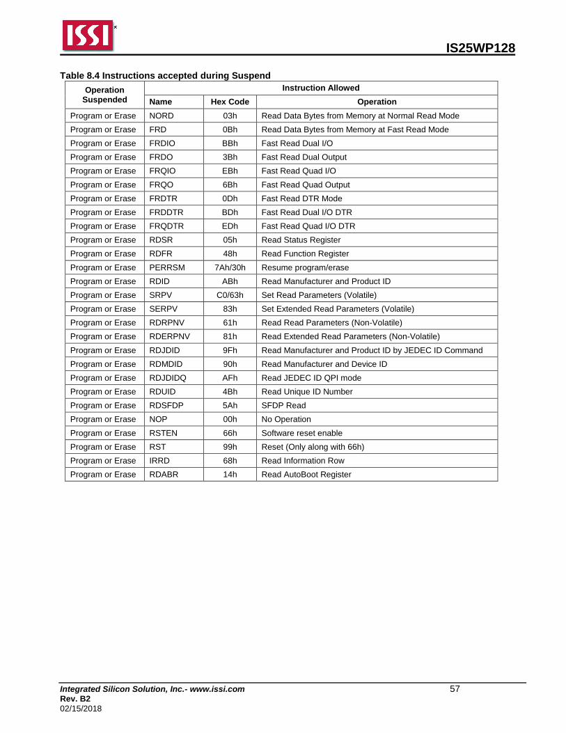
IS25WP128
Integrated Silicon Solution, Inc.- www.issi.com 57 Rev. B2
02/15/2018
Table 8.4 Instructions accepted during Suspend
Operation Suspended
Instruction Allowed
Name Hex Code Operation
Program or Erase NORD 03h Read Data Bytes from Memory at Normal Read Mode
Program or Erase FRD 0Bh Read Data Bytes from Memory at Fast Read Mode
Program or Erase FRDIO BBh Fast Read Dual I/O
Program or Erase FRDO 3Bh Fast Read Dual Output
Program or Erase FRQIO EBh Fast Read Quad I/O
Program or Erase FRQO 6Bh Fast Read Quad Output
Program or Erase FRDTR 0Dh Fast Read DTR Mode
Program or Erase FRDDTR BDh Fast Read Dual I/O DTR
Program or Erase FRQDTR EDh Fast Read Quad I/O DTR
Program or Erase RDSR 05h Read Status Register
Program or Erase RDFR 48h Read Function Register
Program or Erase PERRSM 7Ah/30h Resume program/erase
Program or Erase RDID ABh Read Manufacturer and Product ID
Program or Erase SRPV C0/63h Set Read Parameters (Volatile)
Program or Erase SERPV 83h Set Extended Read Parameters (Volatile)
Program or Erase RDRPNV 61h Read Read Parameters (Non-Volatile)
Program or Erase RDERPNV 81h Read Extended Read Parameters (Non-Volatile)
Program or Erase RDJDID 9Fh Read Manufacturer and Product ID by JEDEC ID Command
Program or Erase RDMDID 90h Read Manufacturer and Device ID
Program or Erase RDJDIDQ AFh Read JEDEC ID QPI mode
Program or Erase RDUID 4Bh Read Unique ID Number
Program or Erase RDSFDP 5Ah SFDP Read
Program or Erase NOP 00h No Operation
Program or Erase RSTEN 66h Software reset enable
Program or Erase RST 99h Reset (Only along with 66h)
Program or Erase IRRD 68h Read Information Row
Program or Erase RDABR 14h Read AutoBoot Register
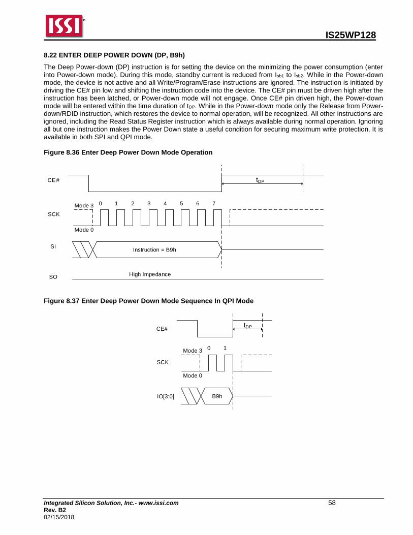
IS25WP128
Integrated Silicon Solution, Inc.- www.issi.com 58 Rev. B2
02/15/2018
8.22 ENTER DEEP POWER DOWN (DP, B9h)
The Deep Power-down (DP) instruction is for setting the device on the minimizing the power consumption (enter into Power-down mode). During this mode, standby current is reduced from Isb1 to Isb2. While in the Power-down mode, the device is not active and all Write/Program/Erase instructions are ignored. The instruction is initiated by driving the CE# pin low and shifting the instruction code into the device. The CE# pin must be driven high after the instruction has been latched, or Power-down mode will not engage. Once CE# pin driven high, the Power-down mode will be entered within the time duration of tDP. While in the Power-down mode only the Release from Power-down/RDID instruction, which restores the device to normal operation, will be recognized. All other instructions are ignored, including the Read Status Register instruction which is always available during normal operation. Ignoring all but one instruction makes the Power Down state a useful condition for securing maximum write protection. It is available in both SPI and QPI mode. Figure 8.36 Enter Deep Power Down Mode Operation
Instruction = B9h
CE#
SCK
SI
0 1 2 3 4 5 6 7Mode 3
Mode 0
tDP
SO High Impedance
Figure 8.37 Enter Deep Power Down Mode Sequence In QPI Mode
B9h
CE#
SCK
IO[3:0]
0 1Mode 3
Mode 0
tDP
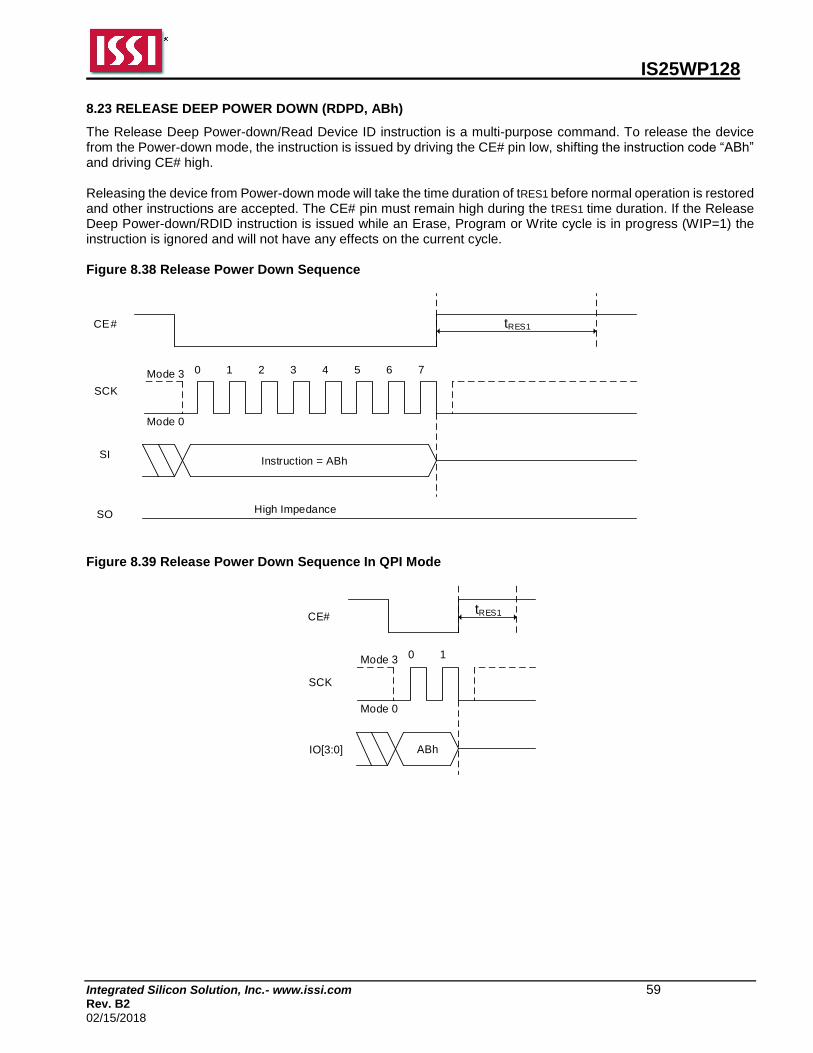
IS25WP128
Integrated Silicon Solution, Inc.- www.issi.com 59 Rev. B2
02/15/2018
8.23 RELEASE DEEP POWER DOWN (RDPD, ABh)
The Release Deep Power-down/Read Device ID instruction is a multi-purpose command. To release the device from the Power-down mode, the instruction is issued by driving the CE# pin low, shifting the instruction code “ABh” and driving CE# high. Releasing the device from Power-down mode will take the time duration of tRES1 before normal operation is restored and other instructions are accepted. The CE# pin must remain high during the tRES1 time duration. If the Release Deep Power-down/RDID instruction is issued while an Erase, Program or Write cycle is in progress (WIP=1) the instruction is ignored and will not have any effects on the current cycle. Figure 8.38 Release Power Down Sequence
tRES1
Instruction = ABh
CE#
SCK
SI
0 1 2 3 4 5 6 7Mode 3
Mode 0
SO High Impedance
Figure 8.39 Release Power Down Sequence In QPI Mode
tRES1
ABh
CE#
SCK
IO[3:0]
0 1Mode 3
Mode 0
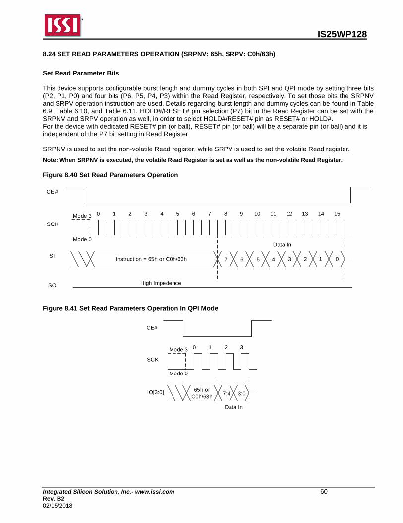
IS25WP128
Integrated Silicon Solution, Inc.- www.issi.com 60 Rev. B2
02/15/2018
8.24 SET READ PARAMETERS OPERATION (SRPNV: 65h, SRPV: C0h/63h)
Set Read Parameter Bits This device supports configurable burst length and dummy cycles in both SPI and QPI mode by setting three bits (P2, P1, P0) and four bits (P6, P5, P4, P3) within the Read Register, respectively. To set those bits the SRPNV and SRPV operation instruction are used. Details regarding burst length and dummy cycles can be found in Table 6.9, Table 6.10, and Table 6.11. HOLD#/RESET# pin selection (P7) bit in the Read Register can be set with the SRPNV and SRPV operation as well, in order to select HOLD#/RESET# pin as RESET# or HOLD#. For the device with dedicated RESET# pin (or ball), RESET# pin (or ball) will be a separate pin (or ball) and it is independent of the P7 bit setting in Read Register SRPNV is used to set the non-volatile Read register, while SRPV is used to set the volatile Read register.
Note: When SRPNV is executed, the volatile Read Register is set as well as the non-volatile Read Register.
Figure 8.40 Set Read Parameters Operation
Instruction = 65h or C0h/63h
CE#
SCK
SI
SO
Data In
0 1 2 3 4 5 6 7 8 9 10 11 12 13 14 15Mode 3
Mode 0
7 3 2 1 06 5 4
High Impedence
Figure 8.41 Set Read Parameters Operation In QPI Mode
65h or
C0h/63h
0 1Mode 3
Mode 0
2 3
7:4 3:0
CE#
SCK
IO[3:0]
Data In
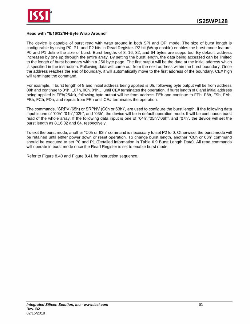
IS25WP128
Integrated Silicon Solution, Inc.- www.issi.com 61 Rev. B2
02/15/2018
Read with “8/16/32/64-Byte Wrap Around”
The device is capable of burst read with wrap around in both SPI and QPI mode. The size of burst length is configurable by using P0, P1, and P2 bits in Read Register. P2 bit (Wrap enable) enables the burst mode feature. P0 and P1 define the size of burst. Burst lengths of 8, 16, 32, and 64 bytes are supported. By default, address increases by one up through the entire array. By setting the burst length, the data being accessed can be limited to the length of burst boundary within a 256 byte page. The first output will be the data at the initial address which is specified in the instruction. Following data will come out from the next address within the burst boundary. Once the address reaches the end of boundary, it will automatically move to the first address of the boundary. CE# high will terminate the command. For example, if burst length of 8 and initial address being applied is 0h, following byte output will be from address 00h and continue to 01h,..,07h, 00h, 01h… until CE# terminates the operation. If burst length of 8 and initial address being applied is FEh(254d), following byte output will be from address FEh and continue to FFh, F8h, F9h, FAh, FBh, FCh, FDh, and repeat from FEh until CE# terminates the operation. The commands, “SRPV (65h) or SRPNV (C0h or 63h)”, are used to configure the burst length. If the following data input is one of “00h”,”01h”,”02h”, and ”03h”, the device will be in default operation mode. It will be continuous burst read of the whole array. If the following data input is one of “04h”,”05h”,”06h”, and ”07h”, the device will set the burst length as 8,16,32 and 64, respectively. To exit the burst mode, another “C0h or 63h” command is necessary to set P2 to 0. Otherwise, the burst mode will be retained until either power down or reset operation. To change burst length, another “C0h or 63h” command should be executed to set P0 and P1 (Detailed information in Table 6.9 Burst Length Data). All read commands will operate in burst mode once the Read Register is set to enable burst mode. Refer to Figure 8.40 and Figure 8.41 for instruction sequence.
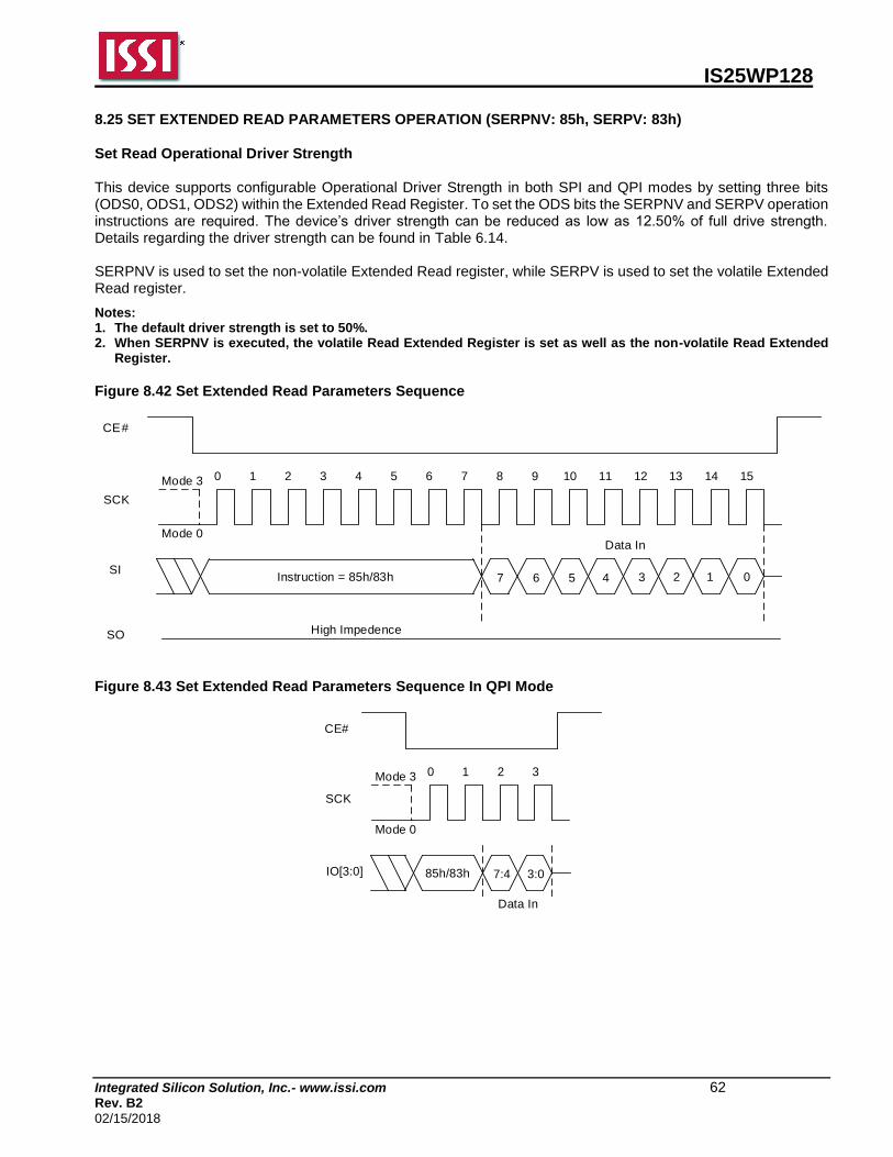
IS25WP128
Integrated Silicon Solution, Inc.- www.issi.com 62 Rev. B2
02/15/2018
8.25 SET EXTENDED READ PARAMETERS OPERATION (SERPNV: 85h, SERPV: 83h)
Set Read Operational Driver Strength This device supports configurable Operational Driver Strength in both SPI and QPI modes by setting three bits (ODS0, ODS1, ODS2) within the Extended Read Register. To set the ODS bits the SERPNV and SERPV operation instructions are required. The device’s driver strength can be reduced as low as 12.50% of full drive strength. Details regarding the driver strength can be found in Table 6.14. SERPNV is used to set the non-volatile Extended Read register, while SERPV is used to set the volatile Extended Read register.
Notes: 1. The default driver strength is set to 50%. 2. When SERPNV is executed, the volatile Read Extended Register is set as well as the non-volatile Read Extended
Register.
Figure 8.42 Set Extended Read Parameters Sequence
Instruction = 85h/83h
CE#
SCK
SI
SO
Data In
0 1 2 3 4 5 6 7 8 9 10 11 12 13 14 15Mode 3
Mode 0
7 3 2 1 06 5 4
High Impedence
Figure 8.43 Set Extended Read Parameters Sequence In QPI Mode
85h/83h
0 1Mode 3
Mode 0
2 3
7:4 3:0
CE#
SCK
IO[3:0]
Data In
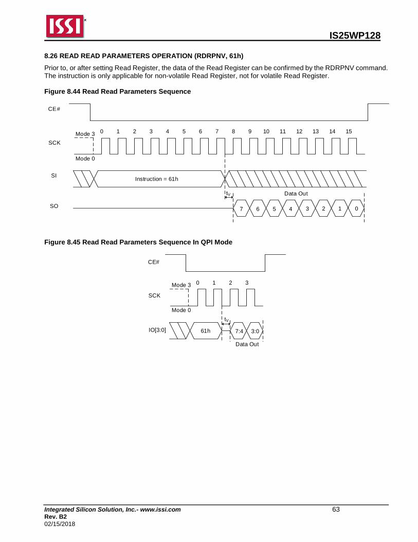
IS25WP128
Integrated Silicon Solution, Inc.- www.issi.com 63 Rev. B2
02/15/2018
8.26 READ READ PARAMETERS OPERATION (RDRPNV, 61h)
Prior to, or after setting Read Register, the data of the Read Register can be confirmed by the RDRPNV command. The instruction is only applicable for non-volatile Read Register, not for volatile Read Register. Figure 8.44 Read Read Parameters Sequence
Instruction = 61h
7
CE#
SCK
SI
3 2SO 1 0
Data Out
6 5
0 1 2 3 4 5 6 7 8 9 10 11 12 13 14 15Mode 3
Mode 0
4
tV
Figure 8.45 Read Read Parameters Sequence In QPI Mode
61h
0 1Mode 3
Mode 0
2 3
7:4 3:0
CE#
SCK
IO[3:0]
tV
Data Out
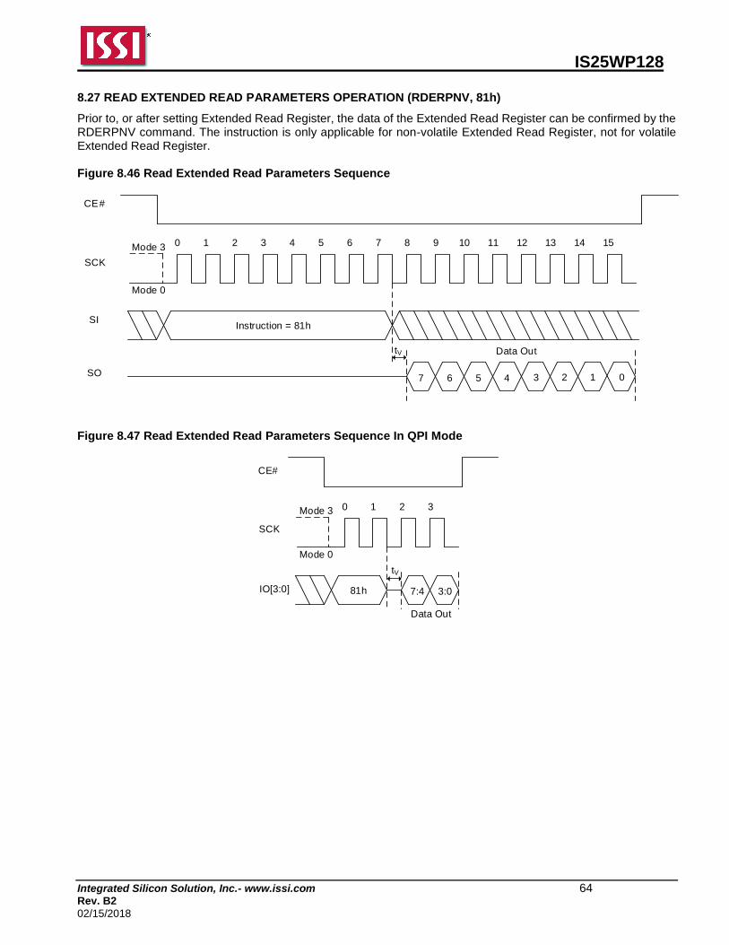
IS25WP128
Integrated Silicon Solution, Inc.- www.issi.com 64 Rev. B2
02/15/2018
8.27 READ EXTENDED READ PARAMETERS OPERATION (RDERPNV, 81h)
Prior to, or after setting Extended Read Register, the data of the Extended Read Register can be confirmed by the RDERPNV command. The instruction is only applicable for non-volatile Extended Read Register, not for volatile Extended Read Register. Figure 8.46 Read Extended Read Parameters Sequence
Instruction = 81h
7
CE#
SCK
SI
3 2SO 1 0
Data Out
6 5
0 1 2 3 4 5 6 7 8 9 10 11 12 13 14 15Mode 3
Mode 0
4
tV
Figure 8.47 Read Extended Read Parameters Sequence In QPI Mode
81h
0 1Mode 3
Mode 0
2 3
7:4 3:0
CE#
SCK
IO[3:0]
tV
Data Out
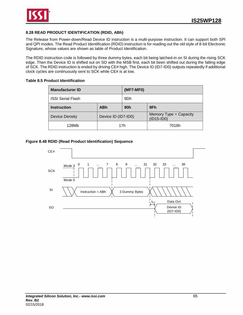
IS25WP128
Integrated Silicon Solution, Inc.- www.issi.com 65 Rev. B2
02/15/2018
8.28 READ PRODUCT IDENTIFICATION (RDID, ABh)
The Release from Power-down/Read Device ID instruction is a multi-purpose instruction. It can support both SPI and QPI modes. The Read Product Identification (RDID) instruction is for reading out the old style of 8-bit Electronic Signature, whose values are shown as table of Product Identification. The RDID instruction code is followed by three dummy bytes, each bit being latched-in on SI during the rising SCK edge. Then the Device ID is shifted out on SO with the MSB first, each bit been shifted out during the falling edge of SCK. The RDID instruction is ended by driving CE# high. The Device ID (ID7-ID0) outputs repeatedly if additional clock cycles are continuously sent to SCK while CE# is at low. Table 8.5 Product Identification
Manufacturer ID (MF7-MF0)
ISSI Serial Flash 9Dh
Instruction ABh 90h 9Fh
Device Density Device ID (ID7-ID0) Memory Type + Capacity (ID15-ID0)
128Mb 17h 7018h
Figure 8.48 RDID (Read Product Identification) Sequence
Device ID
(ID7-ID0)
Data Out
32 33 ... 39
Instruction = ABh
CE#
SCK
SI
SO
0 1 ... 7 8 9 ... 31Mode 3
Mode 0
3 Dummy Bytes
tV
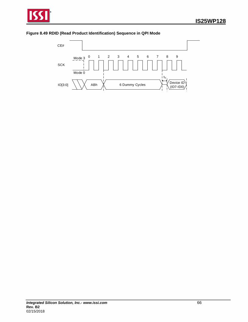
IS25WP128
Integrated Silicon Solution, Inc.- www.issi.com 66 Rev. B2
02/15/2018
Figure 8.49 RDID (Read Product Identification) Sequence in QPI Mode
ABh
CE#
SCK
IO[3:0]
0 1Mode 3
Mode 0
2 3 4 5 6 7 8 9
6 Dummy CyclesDevice ID
(ID7-ID0)
tV
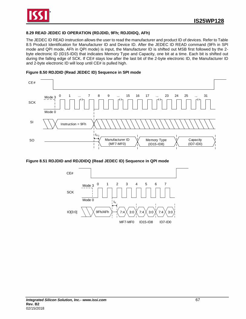
IS25WP128
Integrated Silicon Solution, Inc.- www.issi.com 67 Rev. B2
02/15/2018
8.29 READ JEDEC ID OPERATION (RDJDID, 9Fh; RDJDIDQ, AFh)
The JEDEC ID READ instruction allows the user to read the manufacturer and product ID of devices. Refer to Table 8.5 Product Identification for Manufacturer ID and Device ID. After the JEDEC ID READ command (9Fh in SPI mode and QPI mode, AFh in QPI mode) is input, the Manufacturer ID is shifted out MSB first followed by the 2-byte electronic ID (ID15-ID0) that indicates Memory Type and Capacity, one bit at a time. Each bit is shifted out during the falling edge of SCK. If CE# stays low after the last bit of the 2-byte electronic ID, the Manufacturer ID and 2-byte electronic ID will loop until CE# is pulled high. Figure 8.50 RDJDID (Read JEDEC ID) Sequence in SPI mode
Instruction = 9Fh
Memory Type
(ID15-ID8)
CE#
SCK
SI
Capacity
(ID7-ID0)SO
0 1 ... 7 8 9 ... 15 16 17 ... 23 24 25 ... 31Mode 3
Mode 0
Manufacturer ID
(MF7-MF0)
tV
Figure 8.51 RDJDID and RDJDIDQ (Read JEDEC ID) Sequence in QPI mode
9Fh/AFh
CE#
SCK
IO[3:0]
0 1Mode 3
Mode 0
2 3
7:4 3:0
4 5
7:4 3:0
6 7
7:4 3:0
MF7-MF0 ID15-ID8 ID7-ID0
tV
IS25WP128
Integrated Silicon Solution, Inc.- www.issi.com 68 Rev. B2
02/15/2018
8.30 READ DEVICE MANUFACTURER AND DEVICE ID OPERATION (RDMDID, 90h)
The Read Device Manufacturer and Device ID (RDMDID) instruction allows the user to read the Manufacturer and Device ID of the products. Refer to Table 8.4 Product Identification for Manufacturer ID and Device ID. The RDMDID instruction code is followed by two dummy bytes and one byte address (A7~A0), each bit being latched-in on SI during the rising edge of SCK. If one byte address is initially set as A0 = 0, then the Manufacturer ID is shifted out on SO with the MSB first followed by the Device ID (ID7- ID0). Each bit is shifted out during the falling edge of SCK. If one byte address is initially set as A0 = 1, then Device ID will be read first followed by the Manufacturer ID. The Manufacturer and Device ID can be read continuously alternating between the two until CE# is driven high. Figure 8.52 RDMDID (Read Product Identification) Sequence
Instruction = 90h
Manufacturer ID
(MF7-MF0)
CE#
SCK
SI
Device ID
(ID7-ID0)SO
0 1 ... 7 8 9 ... 31 32 33 ... 39 40 41 ... 47Mode 3
Mode 0
3-byte Address
tV
Notes: 1. ADDRESS A0 = 0, will output the 1-byte Manufacturer ID (MF7-MF0) 1-byte Device ID (ID7-ID0)
ADDRESS A0 = 1, will output the 1-byte Device ID (ID7-ID0) 1-byte Manufacturer ID (MF7-MF0) 2. The Manufacturer and Device ID can be read continuously and will alternate from one to the other until CE# pin is
pulled high.
Figure 8.53 RDMDID (Read Product Identification) Sequence in QPI Mode
90h
CE#
SCK
IO[3:0]
3-byte Address
0 1 2 3 4 5 6 7 8 9 10 11Mode 3
Mode 0
23:20 7:4 3:0 7:4 3:019:16 15:12 11:8 7:4 3:0
tV
Instruction Manufacturer
ID (MF7-MF0)
Device ID
(ID7-ID0) Notes: 1. ADDRESS A0 = 0, will output the 1-byte Manufacturer ID (MF7-MF0) 1-byte Device ID (ID7-ID0)
ADDRESS A0 = 1, will output the 1-byte Device ID (ID7-ID0) 1-byte Manufacturer ID (MF7-MF0) 2. The Manufacturer and Device ID can be read continuously and will alternate from one to the other until CE# pin is
pulled high.
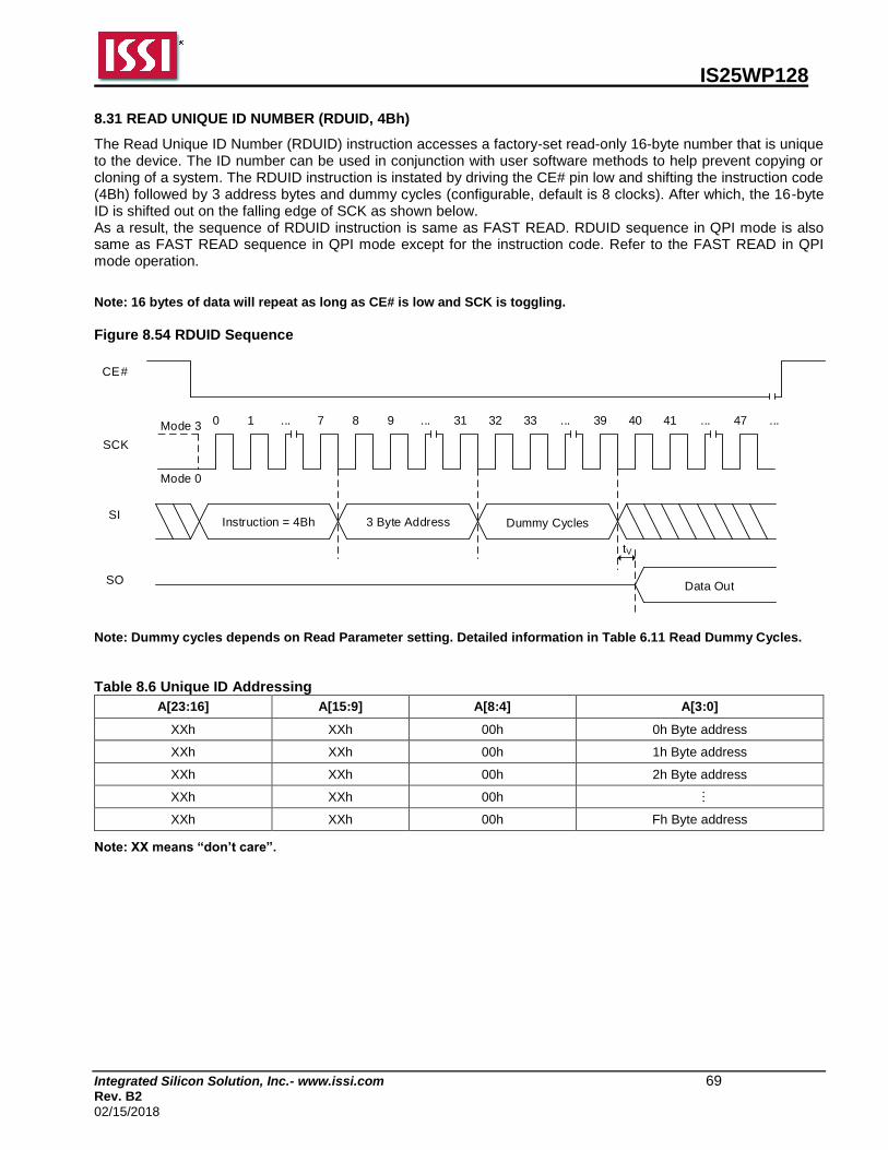
IS25WP128
Integrated Silicon Solution, Inc.- www.issi.com 69 Rev. B2
02/15/2018
8.31 READ UNIQUE ID NUMBER (RDUID, 4Bh)
The Read Unique ID Number (RDUID) instruction accesses a factory-set read-only 16-byte number that is unique to the device. The ID number can be used in conjunction with user software methods to help prevent copying or cloning of a system. The RDUID instruction is instated by driving the CE# pin low and shifting the instruction code (4Bh) followed by 3 address bytes and dummy cycles (configurable, default is 8 clocks). After which, the 16-byte ID is shifted out on the falling edge of SCK as shown below. As a result, the sequence of RDUID instruction is same as FAST READ. RDUID sequence in QPI mode is also same as FAST READ sequence in QPI mode except for the instruction code. Refer to the FAST READ in QPI mode operation.
Note: 16 bytes of data will repeat as long as CE# is low and SCK is toggling.
Figure 8.54 RDUID Sequence
Instruction = 4Bh Dummy Cycles
CE#
SCK
SI
SO
0 1 ... 7 8 9 ... 31 32 33 ... 39 40 41 ... 47Mode 3
Mode 0
3 Byte Address
Data Out
tV
...
Note: Dummy cycles depends on Read Parameter setting. Detailed information in Table 6.11 Read Dummy Cycles. Table 8.6 Unique ID Addressing
A[23:16] A[15:9] A[8:4] A[3:0]
XXh XXh 00h 0h Byte address
XXh XXh 00h 1h Byte address
XXh XXh 00h 2h Byte address
XXh XXh 00h …
XXh XXh 00h Fh Byte address
Note: XX means “don’t care”.
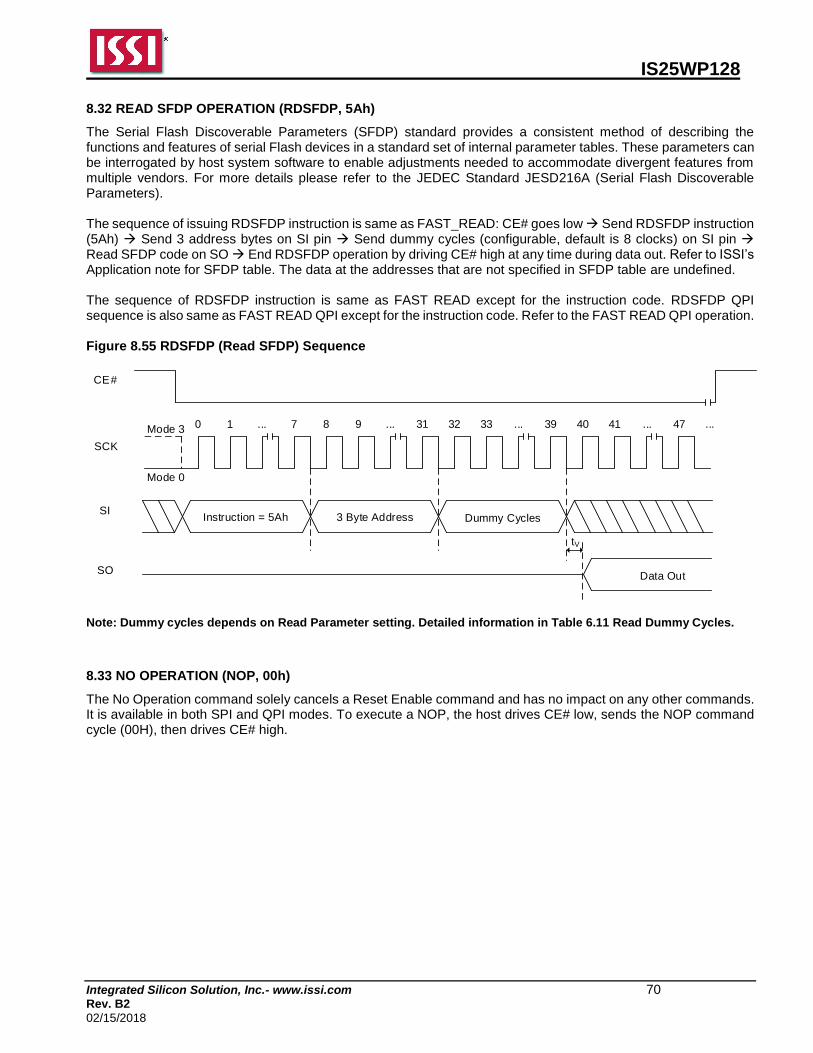
IS25WP128
Integrated Silicon Solution, Inc.- www.issi.com 70 Rev. B2
02/15/2018
8.32 READ SFDP OPERATION (RDSFDP, 5Ah)
The Serial Flash Discoverable Parameters (SFDP) standard provides a consistent method of describing the functions and features of serial Flash devices in a standard set of internal parameter tables. These parameters can be interrogated by host system software to enable adjustments needed to accommodate divergent features from multiple vendors. For more details please refer to the JEDEC Standard JESD216A (Serial Flash Discoverable Parameters). The sequence of issuing RDSFDP instruction is same as FAST_READ: CE# goes low Send RDSFDP instruction (5Ah) Send 3 address bytes on SI pin Send dummy cycles (configurable, default is 8 clocks) on SI pin Read SFDP code on SO End RDSFDP operation by driving CE# high at any time during data out. Refer to ISSI’s Application note for SFDP table. The data at the addresses that are not specified in SFDP table are undefined. The sequence of RDSFDP instruction is same as FAST READ except for the instruction code. RDSFDP QPI sequence is also same as FAST READ QPI except for the instruction code. Refer to the FAST READ QPI operation. Figure 8.55 RDSFDP (Read SFDP) Sequence
Instruction = 5Ah Dummy Cycles
CE#
SCK
SI
SO
0 1 ... 7 8 9 ... 31 32 33 ... 39 40 41 ... 47Mode 3
Mode 0
3 Byte Address
Data Out
tV
...
Note: Dummy cycles depends on Read Parameter setting. Detailed information in Table 6.11 Read Dummy Cycles.
8.33 NO OPERATION (NOP, 00h)
The No Operation command solely cancels a Reset Enable command and has no impact on any other commands. It is available in both SPI and QPI modes. To execute a NOP, the host drives CE# low, sends the NOP command cycle (00H), then drives CE# high.
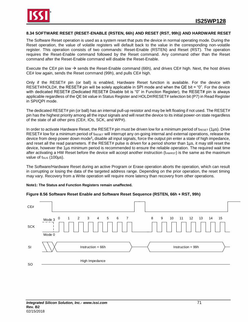
IS25WP128
Integrated Silicon Solution, Inc.- www.issi.com 71 Rev. B2
02/15/2018
8.34 SOFTWARE RESET (RESET-ENABLE (RSTEN, 66h) AND RESET (RST, 99h)) AND HARDWARE RESET
The Software Reset operation is used as a system reset that puts the device in normal operating mode. During the Reset operation, the value of volatile registers will default back to the value in the corresponding non-volatile register. This operation consists of two commands: Reset-Enable (RSTEN) and Reset (RST). The operation requires the Reset-Enable command followed by the Reset command. Any command other than the Reset command after the Reset-Enable command will disable the Reset-Enable. Execute the CE# pin low sends the Reset-Enable command (66h), and drives CE# high. Next, the host drives CE# low again, sends the Reset command (99h), and pulls CE# high. Only if the RESET# pin (or ball) is enabled, Hardware Reset function is available. For the device with RESET#/HOLD#, the RESET# pin will be solely applicable in SPI mode and when the QE bit = “0”. For the device with dedicated RESET# (Dedicated RESET# Disable bit is “0” in Function Register), the RESET# pin is always applicable regardless of the QE bit value in Status Register and HOLD#/RESET# selection bit (P7) in Read Register in SPI/QPI mode. The dedicated RESET# pin (or ball) has an internal pull-up resistor and may be left floating if not used. The RESET# pin has the highest priority among all the input signals and will reset the device to its initial power-on state regardless of the state of all other pins (CE#, IOs, SCK, and WP#). In order to activate Hardware Reset, the RESET# pin must be driven low for a minimum period of tRESET (1µs). Drive RESET# low for a minimum period of tRESET will interrupt any on-going internal and external operations, release the device from deep power down mode1, disable all input signals, force the output pin enter a state of high impedance, and reset all the read parameters. If the RESET# pulse is driven for a period shorter than 1µs, it may still reset the device, however the 1µs minimum period is recommended to ensure the reliable operation. The required wait time after activating a HW Reset before the device will accept another instruction (tHWRST) is the same as the maximum value of tSUS (100µs). The Software/Hardware Reset during an active Program or Erase operation aborts the operation, which can result in corrupting or losing the data of the targeted address range. Depending on the prior operation, the reset timing may vary. Recovery from a Write operation will require more latency than recovery from other operations. Note1: The Status and Function Registers remain unaffected. Figure 8.56 Software Reset Enable and Software Reset Sequence (RSTEN, 66h + RST, 99h)
Instruction = 66h
CE#
SCK
SI
0 1Mode 3
Mode 0
2 3 4 5 6 7
Instruction = 99h
8 9 10 11 12 13 14 15
SOHigh Impedance
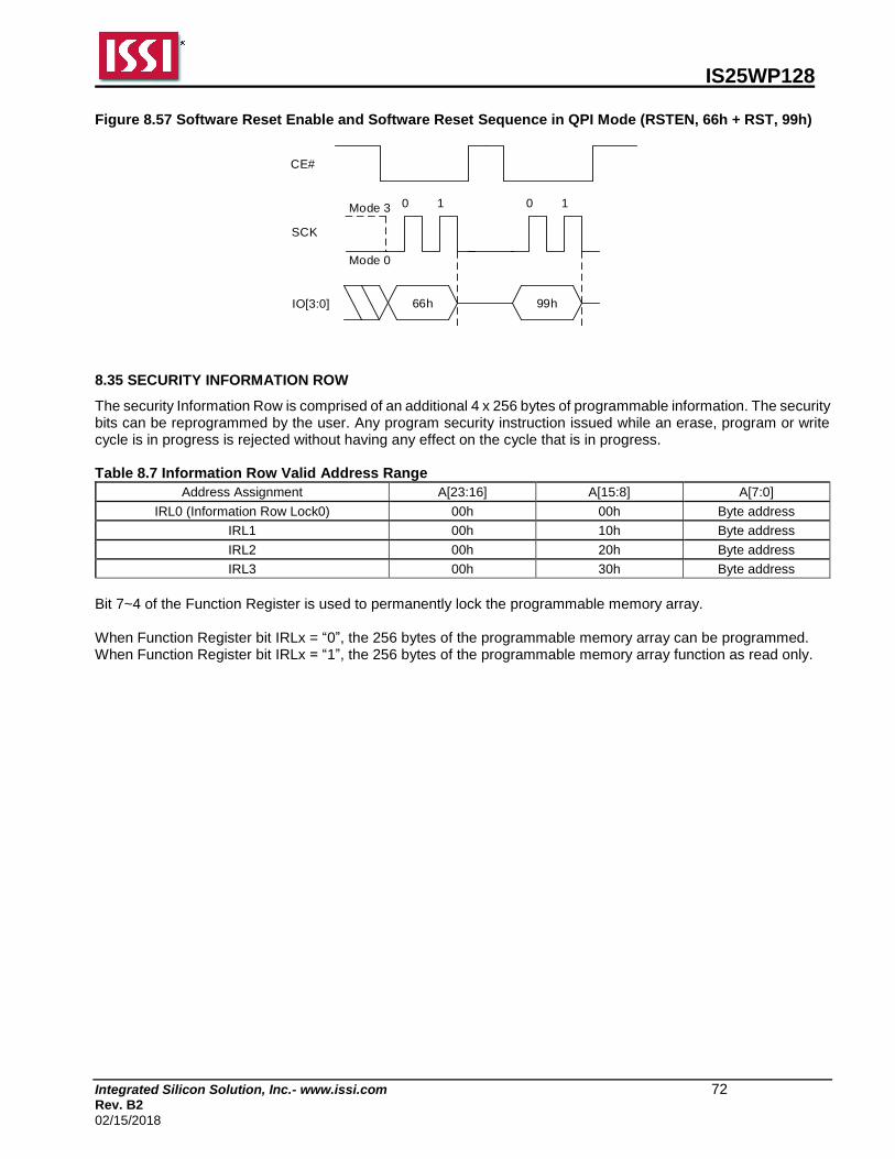
IS25WP128
Integrated Silicon Solution, Inc.- www.issi.com 72 Rev. B2
02/15/2018
Figure 8.57 Software Reset Enable and Software Reset Sequence in QPI Mode (RSTEN, 66h + RST, 99h)
66h
CE#
SCK
IO[3:0]
0 1Mode 3
Mode 0
99h
0 1
8.35 SECURITY INFORMATION ROW
The security Information Row is comprised of an additional 4 x 256 bytes of programmable information. The security bits can be reprogrammed by the user. Any program security instruction issued while an erase, program or write cycle is in progress is rejected without having any effect on the cycle that is in progress. Table 8.7 Information Row Valid Address Range
Address Assignment A[23:16] A[15:8] A[7:0]
IRL0 (Information Row Lock0) 00h 00h Byte address
IRL1 00h 10h Byte address
IRL2 00h 20h Byte address
IRL3 00h 30h Byte address
Bit 7~4 of the Function Register is used to permanently lock the programmable memory array. When Function Register bit IRLx = “0”, the 256 bytes of the programmable memory array can be programmed. When Function Register bit IRLx = “1”, the 256 bytes of the programmable memory array function as read only.
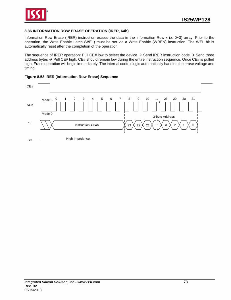
IS25WP128
Integrated Silicon Solution, Inc.- www.issi.com 73 Rev. B2
02/15/2018
8.36 INFORMATION ROW ERASE OPERATION (IRER, 64h)
Information Row Erase (IRER) instruction erases the data in the Information Row x (x: 0~3) array. Prior to the operation, the Write Enable Latch (WEL) must be set via a Write Enable (WREN) instruction. The WEL bit is automatically reset after the completion of the operation. The sequence of IRER operation: Pull CE# low to select the device Send IRER instruction code Send three address bytes Pull CE# high. CE# should remain low during the entire instruction sequence. Once CE# is pulled high, Erase operation will begin immediately. The internal control logic automatically handles the erase voltage and timing. Figure 8.58 IRER (Information Row Erase) Sequence
Instruction = 64h 23
CE#
SCK
SI3 2
SO
1 0
3-byte Address
High Impedance
22 21...
0 1 2 3 4 5 6 7 8 9 10 ... 28 29 30 31Mode 3
Mode 0
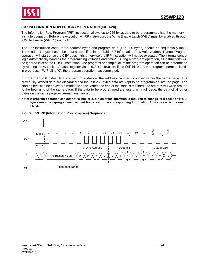
IS25WP128
Integrated Silicon Solution, Inc.- www.issi.com 74 Rev. B2
02/15/2018
8.37 INFORMATION ROW PROGRAM OPERATION (IRP, 62h)
The Information Row Program (IRP) instruction allows up to 256 bytes data to be programmed into the memory in a single operation. Before the execution of IRP instruction, the Write Enable Latch (WEL) must be enabled through a Write Enable (WREN) instruction. The IRP instruction code, three address bytes and program data (1 to 256 bytes) should be sequentially input. Three address bytes has to be input as specified in the Table 8.7 Information Row Valid Address Range. Program operation will start once the CE# goes high, otherwise the IRP instruction will not be executed. The internal control logic automatically handles the programming voltages and timing. During a program operation, all instructions will be ignored except the RDSR instruction. The progress or completion of the program operation can be determined by reading the WIP bit in Status Register via a RDSR instruction. If the WIP bit is “1”, the program operation is still in progress. If WIP bit is “0”, the program operation has completed. If more than 256 bytes data are sent to a device, the address counter rolls over within the same page. The previously latched data are discarded and the last 256 bytes data are kept to be programmed into the page. The starting byte can be anywhere within the page. When the end of the page is reached, the address will wrap around to the beginning of the same page. If the data to be programmed are less than a full page, the data of all other bytes on the same page will remain unchanged.
Note: A program operation can alter “1”s into “0”s, but an erase operation is required to change “0”s back to “1”s. A byte cannot be reprogrammed without first erasing the corresponding Information Row array which is one of IR0~3.
Figure 8.59 IRP (Information Row Program) Sequence
Instruction = 62h 23
CE#
SCK
SI7 6
SO
7
3-byte Address
High Impedance
22 ... 0
Data In 1 Data In 256
0 1 ... 7 8 9 ... 31 32 33 ... 39 ...
20
72
...
20
79
Mode 3
Mode 0
... 0 ... ... 0
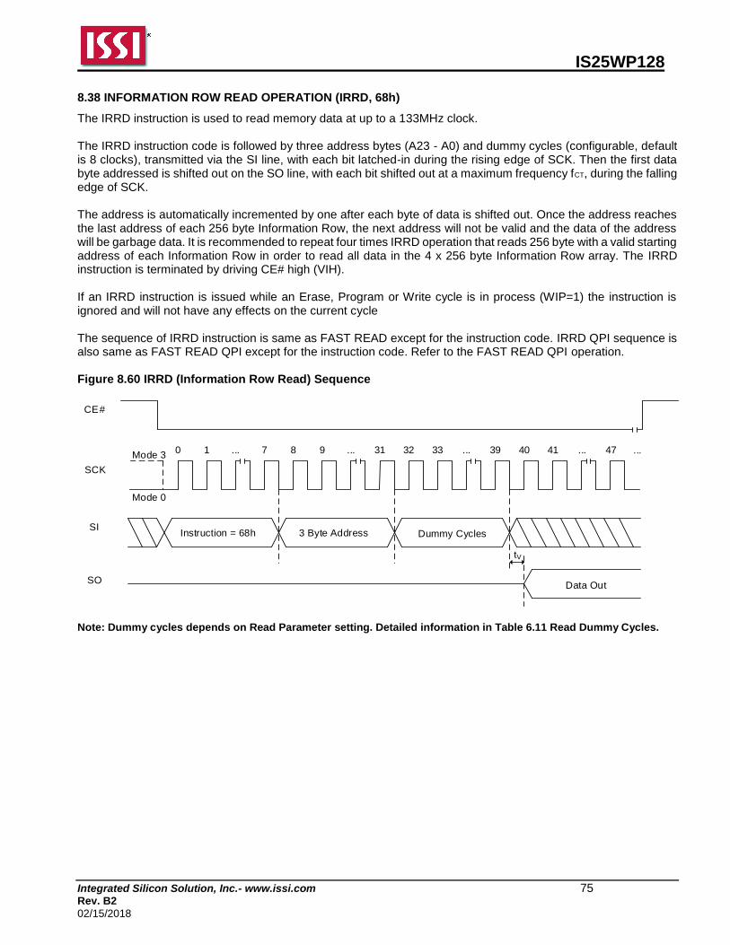
IS25WP128
Integrated Silicon Solution, Inc.- www.issi.com 75 Rev. B2
02/15/2018
8.38 INFORMATION ROW READ OPERATION (IRRD, 68h)
The IRRD instruction is used to read memory data at up to a 133MHz clock. The IRRD instruction code is followed by three address bytes (A23 - A0) and dummy cycles (configurable, default is 8 clocks), transmitted via the SI line, with each bit latched-in during the rising edge of SCK. Then the first data byte addressed is shifted out on the SO line, with each bit shifted out at a maximum frequency fCT, during the falling edge of SCK. The address is automatically incremented by one after each byte of data is shifted out. Once the address reaches the last address of each 256 byte Information Row, the next address will not be valid and the data of the address will be garbage data. It is recommended to repeat four times IRRD operation that reads 256 byte with a valid starting address of each Information Row in order to read all data in the 4 x 256 byte Information Row array. The IRRD instruction is terminated by driving CE# high (VIH). If an IRRD instruction is issued while an Erase, Program or Write cycle is in process (WIP=1) the instruction is ignored and will not have any effects on the current cycle The sequence of IRRD instruction is same as FAST READ except for the instruction code. IRRD QPI sequence is also same as FAST READ QPI except for the instruction code. Refer to the FAST READ QPI operation. Figure 8.60 IRRD (Information Row Read) Sequence
Instruction = 68h Dummy Cycles
CE#
SCK
SI
SO
0 1 ... 7 8 9 ... 31 32 33 ... 39 40 41 ... 47Mode 3
Mode 0
3 Byte Address
Data Out
tV
...
Note: Dummy cycles depends on Read Parameter setting. Detailed information in Table 6.11 Read Dummy Cycles.
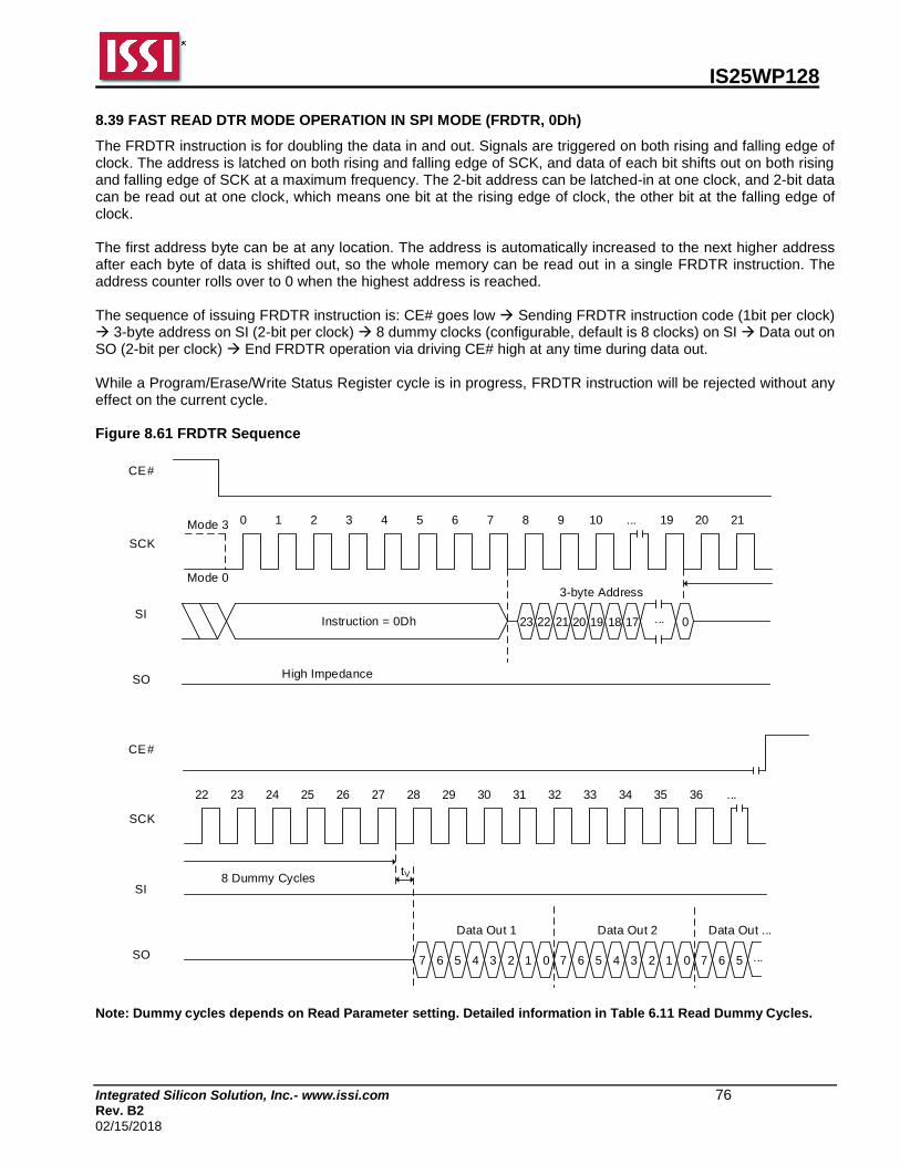
IS25WP128
Integrated Silicon Solution, Inc.- www.issi.com 76 Rev. B2
02/15/2018
8.39 FAST READ DTR MODE OPERATION IN SPI MODE (FRDTR, 0Dh)
The FRDTR instruction is for doubling the data in and out. Signals are triggered on both rising and falling edge of clock. The address is latched on both rising and falling edge of SCK, and data of each bit shifts out on both rising and falling edge of SCK at a maximum frequency. The 2-bit address can be latched-in at one clock, and 2-bit data can be read out at one clock, which means one bit at the rising edge of clock, the other bit at the falling edge of clock. The first address byte can be at any location. The address is automatically increased to the next higher address after each byte of data is shifted out, so the whole memory can be read out in a single FRDTR instruction. The address counter rolls over to 0 when the highest address is reached. The sequence of issuing FRDTR instruction is: CE# goes low Sending FRDTR instruction code (1bit per clock) 3-byte address on SI (2-bit per clock) 8 dummy clocks (configurable, default is 8 clocks) on SI Data out on SO (2-bit per clock) End FRDTR operation via driving CE# high at any time during data out. While a Program/Erase/Write Status Register cycle is in progress, FRDTR instruction will be rejected without any effect on the current cycle. Figure 8.61 FRDTR Sequence
CE#
SCK
SI
SO
Data Out 1
Instruction = 0Dh
CE#
SCK
SI
SO
3-byte Address
High Impedance
0 1 2 3 4 5 6 7 8 9 10 ... 19 20 21
22 23 24 25 26 27 28 29 30 31 32 33 34 35 36 ...
Mode 3
Mode 0
tV
23 22 21 0
7 6 5 4 3 2 1 0
Data Out 2
7 6 5 4 3 2 1 0
Data Out ...
7 6
8 Dummy Cycles
20 19 18 17
5 ...
...
Note: Dummy cycles depends on Read Parameter setting. Detailed information in Table 6.11 Read Dummy Cycles.
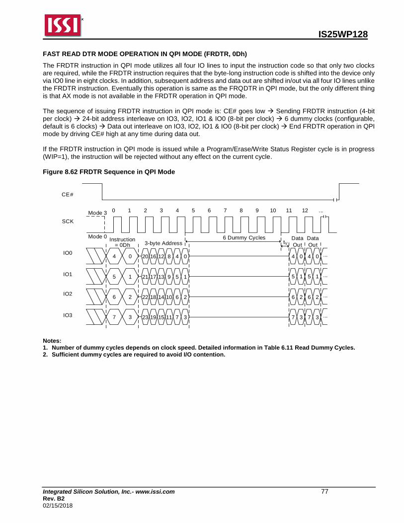
IS25WP128
Integrated Silicon Solution, Inc.- www.issi.com 77 Rev. B2
02/15/2018
FAST READ DTR MODE OPERATION IN QPI MODE (FRDTR, 0Dh)
The FRDTR instruction in QPI mode utilizes all four IO lines to input the instruction code so that only two clocks are required, while the FRDTR instruction requires that the byte-long instruction code is shifted into the device only via IO0 line in eight clocks. In addition, subsequent address and data out are shifted in/out via all four IO lines unlike the FRDTR instruction. Eventually this operation is same as the FRQDTR in QPI mode, but the only different thing is that AX mode is not available in the FRDTR operation in QPI mode. The sequence of issuing FRDTR instruction in QPI mode is: CE# goes low Sending FRDTR instruction (4-bit per clock) 24-bit address interleave on IO3, IO2, IO1 & IO0 (8-bit per clock) 6 dummy clocks (configurable, default is 6 clocks) Data out interleave on IO3, IO2, IO1 & IO0 (8-bit per clock) End FRDTR operation in QPI mode by driving CE# high at any time during data out. If the FRDTR instruction in QPI mode is issued while a Program/Erase/Write Status Register cycle is in progress (WIP=1), the instruction will be rejected without any effect on the current cycle. Figure 8.62 FRDTR Sequence in QPI Mode
Instruction= 0Dh
CE#
SCK
3-byte Address
0 1 2 3 4 5 6 7 8 9 10 11 12Mode 3
Mode 0tV
20 16 12
5 121 17 13
4 0IO0
IO1
22 18 14
23 19 15
8 4 0
9 5 1
10 6 2
11 7 3
6 Dummy Cycles
IO2
IO3
6 2
7 3
5 1
4 0
6 2
7 3
Data
Out
Data
Out
...
4 0
5 1
6 2
7 3
...
...
...
...
Notes: 1. Number of dummy cycles depends on clock speed. Detailed information in Table 6.11 Read Dummy Cycles. 2. Sufficient dummy cycles are required to avoid I/O contention.
IS25WP128
Integrated Silicon Solution, Inc.- www.issi.com 78 Rev. B2
02/15/2018
8.40 FAST READ DUAL IO DTR MODE OPERATION (FRDDTR, BDh)
The FRDDTR instruction enables Double Transfer Rate throughput on dual I/O of the device in read mode. The address (interleave on dual I/O pins) is latched on both rising and falling edge of SCK, and the data (interleave on dual I/O pins) shift out on both rising and falling edge of SCK at a maximum frequency. The 4-bit address can be latched-in at one clock, and 4-bit data can be read out at one clock, which means two bits at the rising edge of clock, the other two bits at the falling edge of clock. The first address byte can be at any location. The address is automatically increased to the next higher address after each byte of data is shifted out, so the whole memory can be read out with a single FRDDTR instruction. The address counter rolls over to 0 when the highest address is reached. Once writing FRDDTR instruction, the following address/dummy/data out will perform as 4-bit instead of previous 1-bit. The sequence of issuing FRDDTR instruction is: CE# goes low Sending FRDDTR instruction (1-bit per clock) 24-bit address interleave on IO1 & IO0 (4-bit per clock) 4 dummy clocks (configurable, default is 4 clocks) on IO1 & IO0 Data out interleave on IO1 & IO0 (4-bit per clock) End FRDDTR operation via pulling CE# high at any time during data out (Please refer to Figure 8.63 for 2 x I/O Double Transfer Rate Read Mode Timing Waveform). If AXh (where X is don’t care) is input for the mode bits during dummy cycles, the device will enter AX read operation mode which enables subsequent FRDDTR execution skips command code. It saves cycles as described in Figure 8.64. When the code is different from AXh, the device exits the AX read operation. After finishing the read operation, device becomes ready to receive a new command. If the FRDDTR instruction is issued while a Program/Erase/Write Status Register cycle is in progress (WIP=1), the instruction will be rejected without any effect on the current cycle.
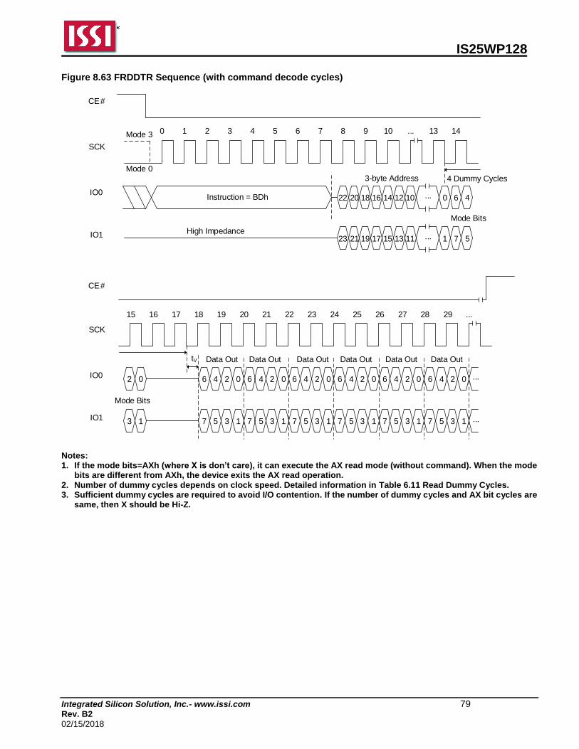
IS25WP128
Integrated Silicon Solution, Inc.- www.issi.com 79 Rev. B2
02/15/2018
Figure 8.63 FRDDTR Sequence (with command decode cycles)
CE#
SCK
IO0
IO1
Instruction = BDh
CE#
SCK
IO0
IO1
3-byte Address
High Impedance
0 1 2 3 4 5 6 7 8 9 10 ... 13 14
15 16 17 18 19 20 21 22 23 24 25 26 27 28 29
Mode 3
Mode 0
...
tV
22 20 18 0
7 5 3 1 7 5 3 1 7 5 3 1 7 5 3 1 7 5 3 1 7 5 3 1
4 Dummy Cycles
23 21 19 1
Data Out
...6 4 2 0 6 4 2 0 6 4 2 0 6 4 2 0 6 4 2 0 6 4 2 0
Data Out Data Out Data Out Data Out Data Out
16 14 12
17 15 13
10
11 7 5
6 4
3 1
2 0
Mode Bits
...
Mode Bits
...
...
Notes: 1. If the mode bits=AXh (where X is don’t care), it can execute the AX read mode (without command). When the mode
bits are different from AXh, the device exits the AX read operation. 2. Number of dummy cycles depends on clock speed. Detailed information in Table 6.11 Read Dummy Cycles. 3. Sufficient dummy cycles are required to avoid I/O contention. If the number of dummy cycles and AX bit cycles are
same, then X should be Hi-Z.
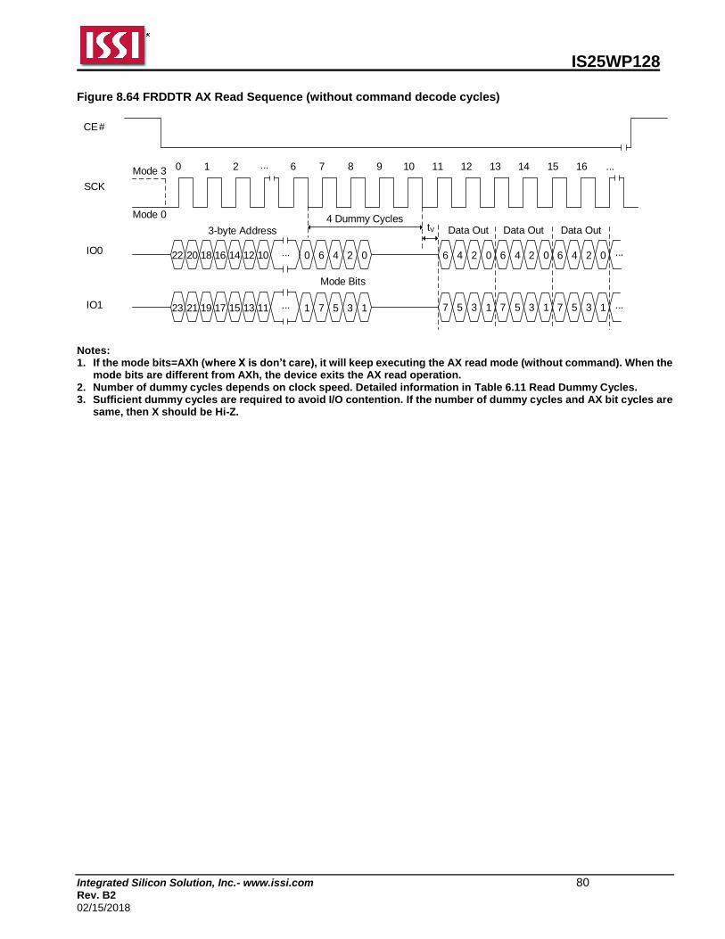
IS25WP128
Integrated Silicon Solution, Inc.- www.issi.com 80 Rev. B2
02/15/2018
Figure 8.64 FRDDTR AX Read Sequence (without command decode cycles)
IO0
IO1
3-byte Address
...
...
tV
22 20 18
7 5 3 1 7 5 3 1 7 5 3 1
4 Dummy Cycles
23 21 19
...6 4 2 0 6 4 2 0 6 4 2 0
Data Out Data Out Data Out
16 14 12
17 15 13
10
11
SCK
0 1 2 ... 6 7 8 9 10 11 12 13 14 15 16Mode 3
Mode 0
CE#
7 5 3 1
6 4 2 00
1
Mode Bits
...
...
Notes: 1. If the mode bits=AXh (where X is don’t care), it will keep executing the AX read mode (without command). When the
mode bits are different from AXh, the device exits the AX read operation. 2. Number of dummy cycles depends on clock speed. Detailed information in Table 6.11 Read Dummy Cycles. 3. Sufficient dummy cycles are required to avoid I/O contention. If the number of dummy cycles and AX bit cycles are
same, then X should be Hi-Z.

IS25WP128
Integrated Silicon Solution, Inc.- www.issi.com 81 Rev. B2
02/15/2018
8.41 FAST READ QUAD IO DTR MODE OPERATION IN SPI MODE (FRQDTR, EDh)
The FRQDTR instruction enables Double Transfer Rate throughput on quad I/O of the device in read mode. A Quad Enable (QE) bit of Status Register must be set to "1" before sending the FRQDTR instruction. The address (interleave on 4 I/O pins) is latched on both rising and falling edge of SCK, and data (interleave on 4 I/O pins) shift out on both rising and falling edge of SCK at a maximum frequency. The 8-bit address can be latched-in at one clock, and 8-bit data can be read out at one clock, which means four bits at the rising edge of clock, the other four bits at the falling edge of clock. The first address byte can be at any location. The address is automatically increased to the next higher address after each byte data is shifted out, so the whole memory can be read out with a single FRQDTR instruction. The address counter rolls over to 0 when the highest address is reached. Once writing FRQDTR instruction, the following address/dummy/data out will perform as 8-bit instead of previous 1-bit. The sequence of issuing FRQDTR instruction is: CE# goes low Sending FRQDTR instruction (1-bit per clock) 24-bit address interleave on IO3, IO2, IO1 & IO0 (8-bit per clock) 6 dummy clocks (configurable, default is 6 clocks) Data out interleave on IO3, IO2, IO1 & IO0 (8-bit per clock) End FRQDTR operation by driving CE# high at any time during data out. If AXh (where X is don’t care) is input for the mode bits during dummy cycles, the device will enter AX read operation mode which enables subsequent FRQDTR execution skips command code. It saves cycles as described in Figure 8.66. When the code is different from AXh, the device exits the AX read operation. After finishing the read operation, device becomes ready to receive a new command. If the FRQDTR instruction is issued while a Program/Erase/Write Status Register cycle is in progress (WIP=1), the instruction will be rejected without any effect on the current cycle.
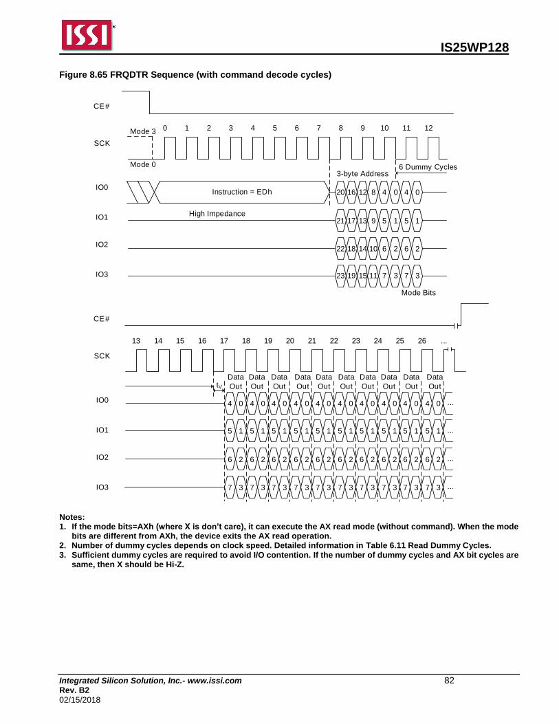
IS25WP128
Integrated Silicon Solution, Inc.- www.issi.com 82 Rev. B2
02/15/2018
Figure 8.65 FRQDTR Sequence (with command decode cycles)
CE#
SCK
Instruction = EDh
CE#
SCK
3-byte Address
High Impedance
0 1 2 3 4 5 6 7 8 9 10 11 12
14 15 16 17 18 19 20 21 22 23 24 25 26 ...
Mode 3
Mode 0
tV
20 16 12
5 1
21 17 13
Data
Out
4 0
IO0
IO1
IO0
22 18 14
23 19 15
8 4 0
9 5 1
10 6 2
11 7 3
6 Dummy Cycles
IO2
IO3
IO1
IO2
IO3
6 2
7 3
5 1
4 0
6 2
7 3
5 1
4 0
6 2
7 3
5 1
4 0
6 2
7 3
5 1
4 0
6 2
7 3
5 1
4 0
6 2
7 3
5 1
4 0
6 2
7 3
5 1
4 0
6 2
7 3
5 1
4 0
6 2
7 3
5 1
4 0
6 2
7 3
Data
Out
Data
Out
Data
Out
Data
Out
Data
Out
Data
Out
Data
Out
Data
Out
Data
Out
13
5 1
4 0
6 2
7 3
Mode Bits
...
...
...
...
Notes: 1. If the mode bits=AXh (where X is don’t care), it can execute the AX read mode (without command). When the mode
bits are different from AXh, the device exits the AX read operation. 2. Number of dummy cycles depends on clock speed. Detailed information in Table 6.11 Read Dummy Cycles. 3. Sufficient dummy cycles are required to avoid I/O contention. If the number of dummy cycles and AX bit cycles are
same, then X should be Hi-Z.
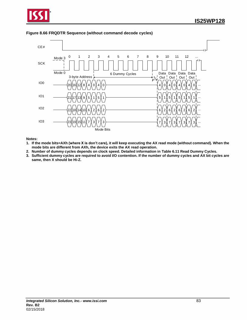
IS25WP128
Integrated Silicon Solution, Inc.- www.issi.com 83 Rev. B2
02/15/2018
Figure 8.66 FRQDTR Sequence (without command decode cycles)
CE#
SCK
3-byte Address
0 1 2 3 4 5 6 7 8 9 10 11Mode 3
Mode 0
tV
20 16 12
5 121 17 13
4 0IO0
IO1
22 18 14
23 19 15
8 4 0
9 5 1
10 6 2
11 7 3
6 Dummy Cycles
IO2
IO3
6 2
7 3
5 1
4 0
6 2
7 3
5 1
4 0
6 2
7 3
5 1
4 0
6 2
7 3
Data
Out
Data
Out
Data
Out
Data
Out
5 1
4 0
6 2
7 3
Mode Bits
12 ...
...
...
...
...
Notes: 1. If the mode bits=AXh (where X is don’t care), it will keep executing the AX read mode (without command). When the
mode bits are different from AXh, the device exits the AX read operation. 2. Number of dummy cycles depends on clock speed. Detailed information in Table 6.11 Read Dummy Cycles. 3. Sufficient dummy cycles are required to avoid I/O contention. If the number of dummy cycles and AX bit cycles are
same, then X should be Hi-Z.
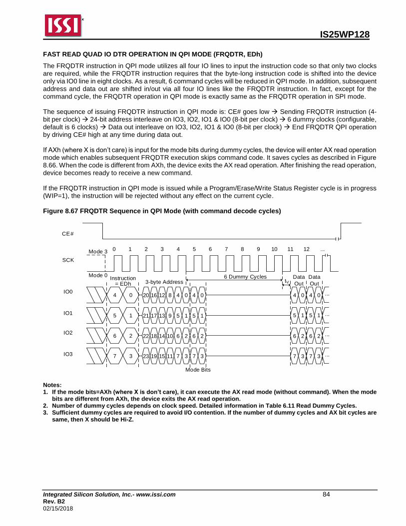
IS25WP128
Integrated Silicon Solution, Inc.- www.issi.com 84 Rev. B2
02/15/2018
FAST READ QUAD IO DTR OPERATION IN QPI MODE (FRQDTR, EDh)
The FRQDTR instruction in QPI mode utilizes all four IO lines to input the instruction code so that only two clocks are required, while the FRQDTR instruction requires that the byte-long instruction code is shifted into the device only via IO0 line in eight clocks. As a result, 6 command cycles will be reduced in QPI mode. In addition, subsequent address and data out are shifted in/out via all four IO lines like the FRQDTR instruction. In fact, except for the command cycle, the FRQDTR operation in QPI mode is exactly same as the FRQDTR operation in SPI mode. The sequence of issuing FRQDTR instruction in QPI mode is: CE# goes low Sending FRQDTR instruction (4-bit per clock) 24-bit address interleave on IO3, IO2, IO1 & IO0 (8-bit per clock) 6 dummy clocks (configurable, default is 6 clocks) Data out interleave on IO3, IO2, IO1 & IO0 (8-bit per clock) End FRQDTR QPI operation by driving CE# high at any time during data out. If AXh (where X is don’t care) is input for the mode bits during dummy cycles, the device will enter AX read operation mode which enables subsequent FRQDTR execution skips command code. It saves cycles as described in Figure 8.66. When the code is different from AXh, the device exits the AX read operation. After finishing the read operation, device becomes ready to receive a new command. If the FRQDTR instruction in QPI mode is issued while a Program/Erase/Write Status Register cycle is in progress (WIP=1), the instruction will be rejected without any effect on the current cycle. Figure 8.67 FRQDTR Sequence in QPI Mode (with command decode cycles)
Instruction= EDh
CE#
SCK
3-byte Address
0 1 2 3 4 5 6 7 8 9 10 11 12Mode 3
Mode 0tV
20 16 12
5 121 17 13
4 0IO0
IO1
22 18 14
23 19 15
8 4 0
9 5 1
10 6 2
11 7 3
6 Dummy Cycles
IO2
IO3
6 2
7 3
5 1
4 0
6 2
7 3
Data
Out
Data
Out
5 1
4 0
6 2
7 3
Mode Bits
...
4 0
5 1
6 2
7 3
...
...
...
...
Notes: 1. If the mode bits=AXh (where X is don’t care), it can execute the AX read mode (without command). When the mode
bits are different from AXh, the device exits the AX read operation. 2. Number of dummy cycles depends on clock speed. Detailed information in Table 6.11 Read Dummy Cycles. 3. Sufficient dummy cycles are required to avoid I/O contention. If the number of dummy cycles and AX bit cycles are
same, then X should be Hi-Z.
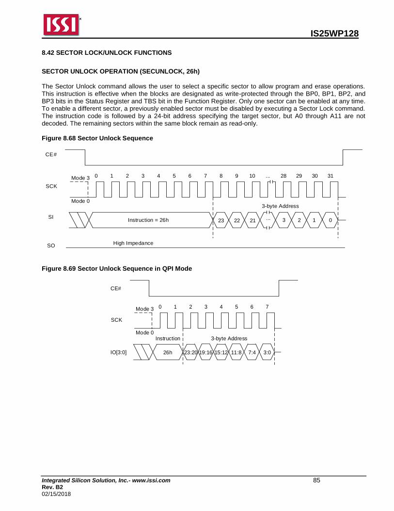
IS25WP128
Integrated Silicon Solution, Inc.- www.issi.com 85 Rev. B2
02/15/2018
8.42 SECTOR LOCK/UNLOCK FUNCTIONS
SECTOR UNLOCK OPERATION (SECUNLOCK, 26h) The Sector Unlock command allows the user to select a specific sector to allow program and erase operations. This instruction is effective when the blocks are designated as write-protected through the BP0, BP1, BP2, and BP3 bits in the Status Register and TBS bit in the Function Register. Only one sector can be enabled at any time. To enable a different sector, a previously enabled sector must be disabled by executing a Sector Lock command. The instruction code is followed by a 24-bit address specifying the target sector, but A0 through A11 are not decoded. The remaining sectors within the same block remain as read-only. Figure 8.68 Sector Unlock Sequence
Instruction = 26h 23
CE#
SCK
SI3 2
SO
1 0
3-byte Address
High Impedance
22 21 ...
0 1 2 3 4 5 6 7 8 9 10 ... 28 29 30 31Mode 3
Mode 0
Figure 8.69 Sector Unlock Sequence in QPI Mode
26h
CE#
SCK
IO[3:0]
3-byte Address
0 1 2 3 4 5 6 7Mode 3
Mode 0
23:20 19:16 15:12 11:8 7:4 3:0
Instruction
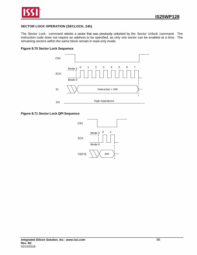
IS25WP128
Integrated Silicon Solution, Inc.- www.issi.com 86 Rev. B2
02/15/2018
SECTOR LOCK OPERATION (SECLOCK, 24h) The Sector Lock command relocks a sector that was previously unlocked by the Sector Unlock command. The instruction code does not require an address to be specified, as only one sector can be enabled at a time. The remaining sectors within the same block remain in read-only mode. Figure 8.70 Sector Lock Sequence
Instruction = 24h
CE#
SCK
SI
0 1 2 3 4 5 6 7Mode 3
Mode 0
SOHigh Impedance
Figure 8.71 Sector Lock QPI Sequence
24h
CE#
SCK
IO[3:0]
0 1Mode 3
Mode 0
IS25WP128
Integrated Silicon Solution, Inc.- www.issi.com 87 Rev. B2
02/15/2018
8.43 AUTOBOOT
SPI devices normally require 32 or more cycles of command and address shifting to initiate a read command. And, in order to read boot code from an SPI device, the host memory controller or processor must supply the read command from a hardwired state machine or from some host processor internal ROM code. Parallel NOR devices need only an initial address, supplied in parallel in a single cycle, and initial access time to start reading boot code. The AutoBoot feature allows the host memory controller to take boot code from the device immediately after the end of reset, without having to send a read command. This saves 32 or more cycles and simplifies the logic needed to initiate the reading of boot code.
As part of the power up reset, hardware reset, or command reset process the AutoBoot feature automatically starts a read access from a pre-specified address. At the time the reset process is completed, the device is ready to deliver code from the starting address. The host memory controller only needs to drive CE# signal from high to low and begin toggling the SCK signal. The device will delay code output for a pre-specified number of clock cycles before code streams out.
– The Auto Boot Start Delay (ABSD) field of the AutoBoot Register specifies the initial delay if any is needed
by the host. – The host cannot send commands during this time. – If QE bit (Bit 6) in the Status Register is set to “1”, Fast Read Quad I/O operation will be selected and initial
delay is the same as dummy cycles of Fast Read Quad I/O Read operation. If it is set to “0”, Fast Read operation will be applied and initial delay is the same as dummy cycles of Fast Read operation. Maximum operation frequency will be 133MHz for both operations.
The starting address of the boot code is selected by the value programmed into the AutoBoot Start Address (ABSA) field of the AutoBoot Register
– Data will continuously shift out until CE# returns high.
At any point after the first data byte is transferred, when CE# returns high, the SPI device will reset to standard SPI mode; able to accept normal command operations.
– A minimum of one byte must be transferred. – AutoBoot mode will not initiate again until another power cycle or a reset occurs.
An AutoBoot Enable bit (ABE) is set to enable the AutoBoot feature. The AutoBoot Register bits are non-volatile and provide:
The starting address set by the AutoBoot Start Address (ABSA).
The number of initial delay cycles, set by the AutoBoot Start Delay (ABSD) 4-bit count value.
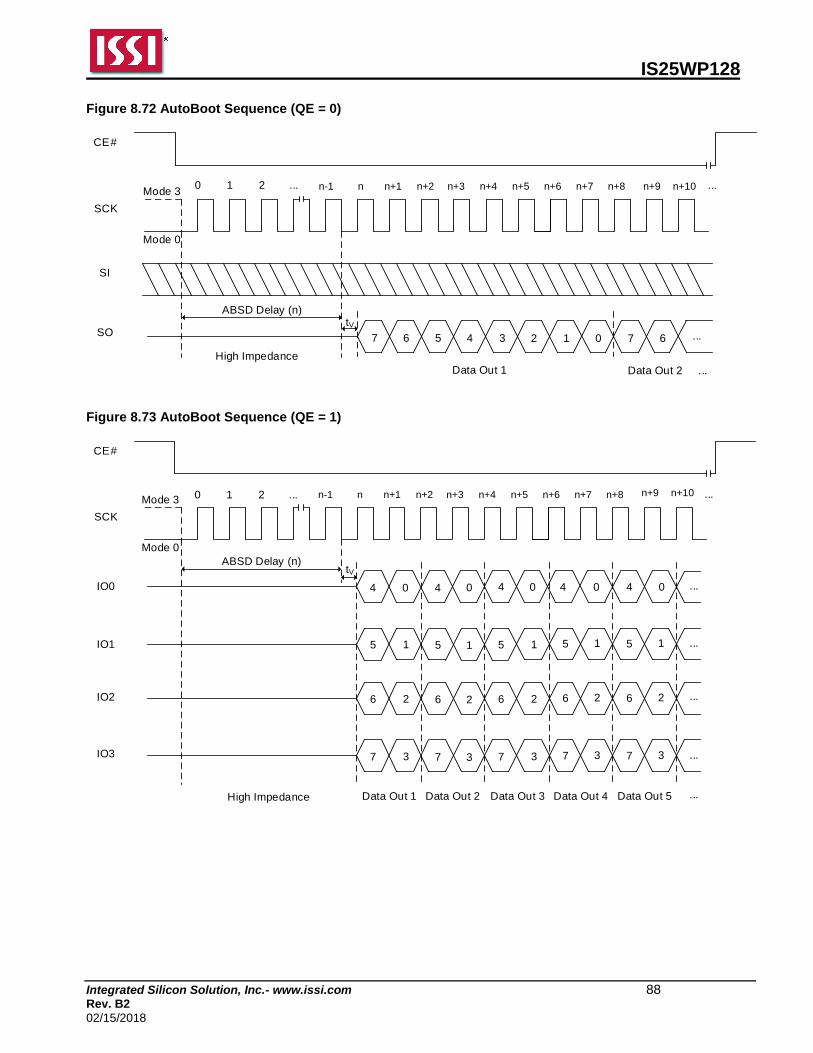
IS25WP128
Integrated Silicon Solution, Inc.- www.issi.com 88 Rev. B2
02/15/2018
Figure 8.72 AutoBoot Sequence (QE = 0)
7
CE#
SCK
SI
3 2SO
1 0
Data Out 1
High Impedance
6 5 4
0 1 2 ... n-1 n n+1 n+2 n+3 n+4 n+5 n+6 n+7 n+8 n+9 n+10Mode 3
Mode 0
tV
ABSD Delay (n)
7 6 ...
Data Out 2 ...
...
Figure 8.73 AutoBoot Sequence (QE = 1)
4
CE#
SCK
4 0 4 0
High Impedance
0 4 0
Mode 3
Mode 0
IO0
IO1
IO2
IO3
5 1
Data Out 1
5 1 5 1 5 1
7 3
6 2
7 3 7 3
6 2 6 2
7 3
6 2
Data Out 2 Data Out 3 Data Out 4
tVABSD Delay (n)
0 1 2 ... n-1 n n+1 n+2 n+3 n+4 n+5 n+6 n+7 n+8 n+9 n+10 ...
4 0
5 1 ...
7 3 ...
6 2 ...
Data Out 5
...
...
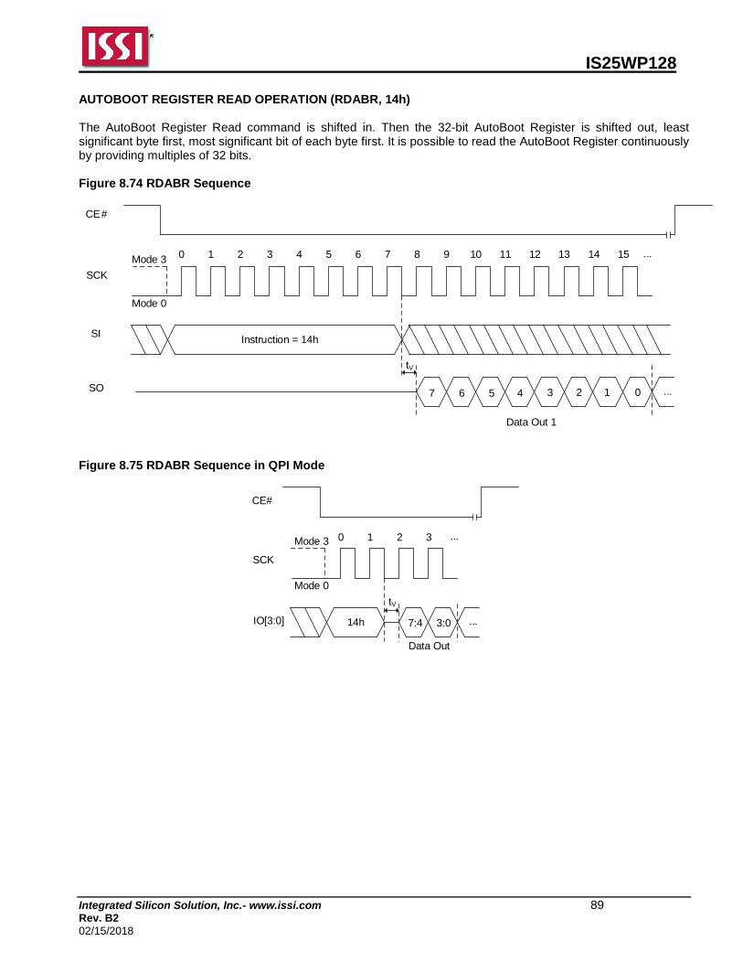
IS25WP128
Integrated Silicon Solution, Inc.- www.issi.com 89 Rev. B2
02/15/2018
AUTOBOOT REGISTER READ OPERATION (RDABR, 14h) The AutoBoot Register Read command is shifted in. Then the 32-bit AutoBoot Register is shifted out, least significant byte first, most significant bit of each byte first. It is possible to read the AutoBoot Register continuously by providing multiples of 32 bits. Figure 8.74 RDABR Sequence
Instruction = 14h
7
CE#
SCK
SI
3 2SO 1 0
Data Out 1
6 5
0 1 2 3 4 5 6 7 8 9 10 11 12 13 14 15Mode 3
Mode 0
4
tV
...
...
Figure 8.75 RDABR Sequence in QPI Mode
14h
0 1Mode 3
Mode 0
2 3
7:4 3:0
CE#
SCK
IO[3:0]
tV
Data Out
...
...
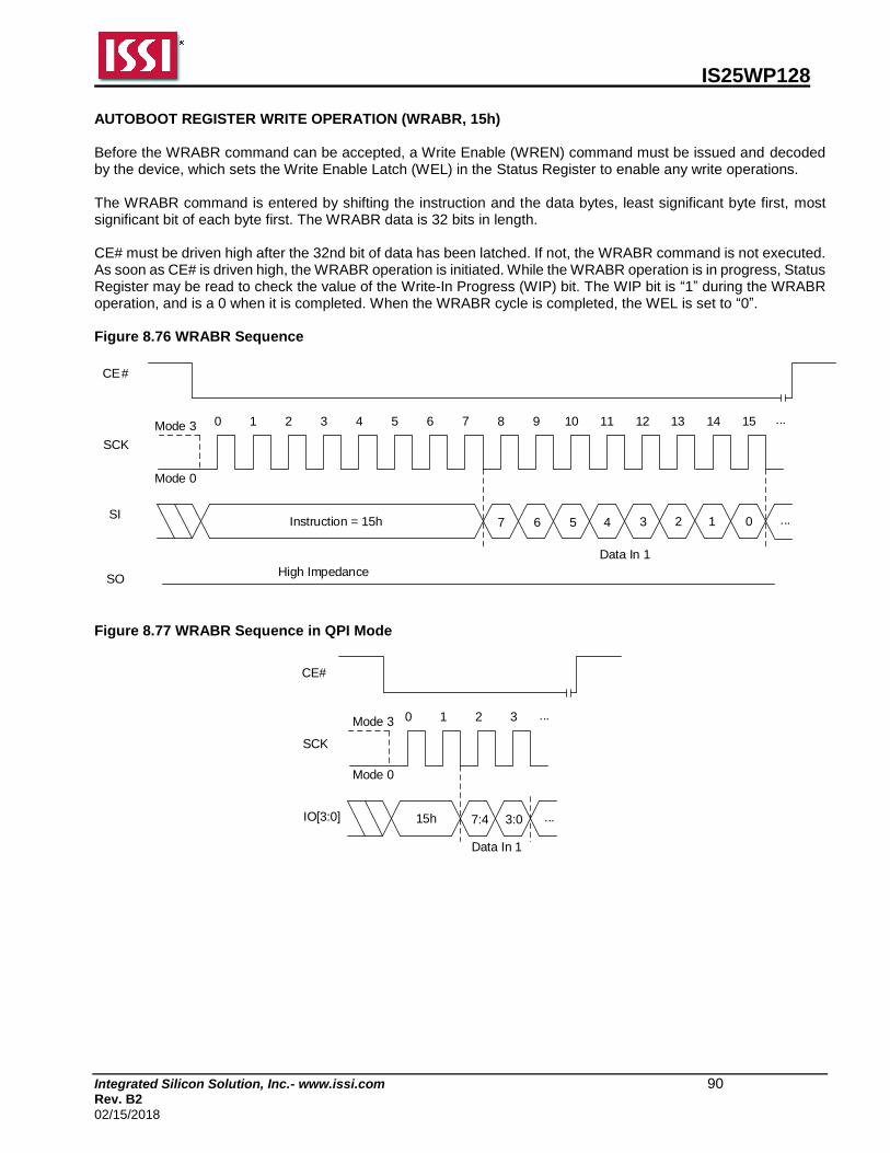
IS25WP128
Integrated Silicon Solution, Inc.- www.issi.com 90 Rev. B2
02/15/2018
AUTOBOOT REGISTER WRITE OPERATION (WRABR, 15h) Before the WRABR command can be accepted, a Write Enable (WREN) command must be issued and decoded by the device, which sets the Write Enable Latch (WEL) in the Status Register to enable any write operations. The WRABR command is entered by shifting the instruction and the data bytes, least significant byte first, most significant bit of each byte first. The WRABR data is 32 bits in length. CE# must be driven high after the 32nd bit of data has been latched. If not, the WRABR command is not executed. As soon as CE# is driven high, the WRABR operation is initiated. While the WRABR operation is in progress, Status Register may be read to check the value of the Write-In Progress (WIP) bit. The WIP bit is “1” during the WRABR operation, and is a 0 when it is completed. When the WRABR cycle is completed, the WEL is set to “0”. Figure 8.76 WRABR Sequence
Instruction = 15h 7
CE#
SCK
SI3 2
SO
1 0
Data In 1
6 5
0 1 2 3 4 5 6 7 8 9 10 11 12 13 14 15Mode 3
Mode 0
4
High Impedance
...
...
Figure 8.77 WRABR Sequence in QPI Mode
15h
0 1Mode 3
Mode 0
2 3
7:4 3:0
CE#
SCK
IO[3:0]
Data In 1
...
...
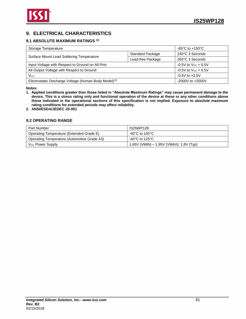
IS25WP128
Integrated Silicon Solution, Inc.- www.issi.com 91 Rev. B2
02/15/2018
9. ELECTRICAL CHARACTERISTICS
9.1 ABSOLUTE MAXIMUM RATINGS (1)
Storage Temperature -65°C to +150°C
Surface Mount Lead Soldering Temperature Standard Package 240°C 3 Seconds
Lead-free Package 260°C 3 Seconds
Input Voltage with Respect to Ground on All Pins -0.5V to VCC + 0.5V
All Output Voltage with Respect to Ground -0.5V to VCC + 0.5V
VCC -0.5V to +2.5V
Electrostatic Discharge Voltage (Human Body Model)(2) -2000V to +2000V
Notes: 1. Applied conditions greater than those listed in “Absolute Maximum Ratings” may cause permanent damage to the
device. This is a stress rating only and functional operation of the device at these or any other conditions above those indicated in the operational sections of this specification is not implied. Exposure to absolute maximum rating conditions for extended periods may affect reliability.
2. ANSI/ESDA/JEDEC JS-001
9.2 OPERATING RANGE
Part Number IS25WP128
Operating Temperature (Extended Grade E) -40°C to 105°C
Operating Temperature (Automotive Grade A3) -40°C to 125°C
VCC Power Supply 1.65V (VMIN) – 1.95V (VMAX); 1.8V (Typ)
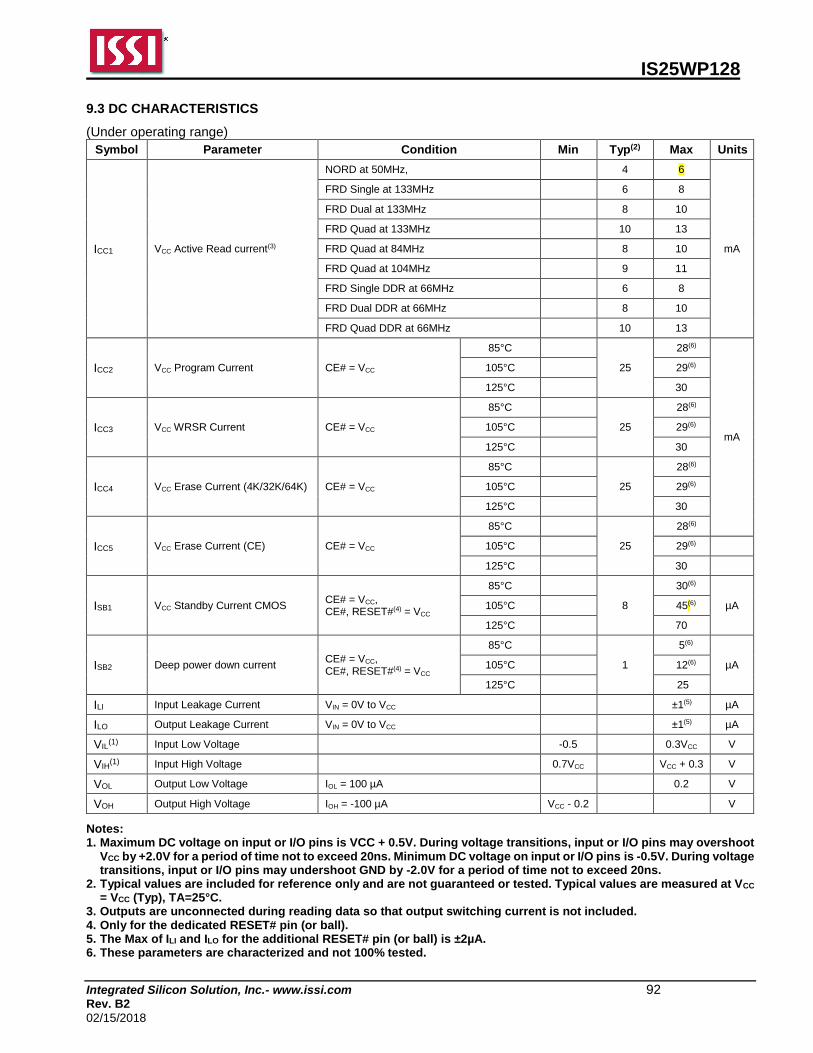
IS25WP128
Integrated Silicon Solution, Inc.- www.issi.com 92 Rev. B2
02/15/2018
9.3 DC CHARACTERISTICS
(Under operating range)
Symbol Parameter Condition Min Typ(2) Max Units
ICC1 VCC Active Read current(3)
NORD at 50MHz, 4 6
mA
FRD Single at 133MHz 6 8
FRD Dual at 133MHz 8 10
FRD Quad at 133MHz 10 13
FRD Quad at 84MHz 8 10
FRD Quad at 104MHz 9 11
FRD Single DDR at 66MHz 6 8
FRD Dual DDR at 66MHz 8 10
FRD Quad DDR at 66MHz 10 13
ICC2 VCC Program Current CE# = VCC
85°C
25
28(6)
mA
105°C 29(6)
125°C 30
ICC3 VCC WRSR Current CE# = VCC
85°C
25
28(6)
105°C 29(6)
125°C 30
ICC4 VCC Erase Current (4K/32K/64K) CE# = VCC
85°C
25
28(6)
105°C 29(6)
125°C 30
ICC5 VCC Erase Current (CE) CE# = VCC
85°C
25
28(6)
105°C 29(6)
125°C 30
ISB1 VCC Standby Current CMOS CE# = VCC, CE#, RESET#(4) = VCC
85°C
8
30(6)
µA 105°C 45(6)
125°C 70
ISB2 Deep power down current CE# = VCC, CE#, RESET#(4) = VCC
85°C
1
5(6)
µA 105°C 12(6)
125°C 25
ILI Input Leakage Current VIN = 0V to VCC ±1(5) µA
ILO Output Leakage Current VIN = 0V to VCC ±1(5) µA
VIL(1) Input Low Voltage -0.5 0.3VCC V
VIH(1) Input High Voltage 0.7VCC VCC + 0.3 V
VOL Output Low Voltage IOL = 100 µA 0.2 V
VOH Output High Voltage IOH = -100 µA VCC - 0.2 V
Notes: 1. Maximum DC voltage on input or I/O pins is VCC + 0.5V. During voltage transitions, input or I/O pins may overshoot
VCC by +2.0V for a period of time not to exceed 20ns. Minimum DC voltage on input or I/O pins is -0.5V. During voltage transitions, input or I/O pins may undershoot GND by -2.0V for a period of time not to exceed 20ns.
2. Typical values are included for reference only and are not guaranteed or tested. Typical values are measured at VCC = VCC (Typ), TA=25°C.
3. Outputs are unconnected during reading data so that output switching current is not included. 4. Only for the dedicated RESET# pin (or ball). 5. The Max of ILI and ILO for the additional RESET# pin (or ball) is ±2µA. 6. These parameters are characterized and not 100% tested.
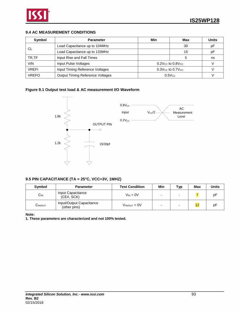
IS25WP128
Integrated Silicon Solution, Inc.- www.issi.com 93 Rev. B2
02/15/2018
9.4 AC MEASUREMENT CONDITIONS
Symbol Parameter Min Max Units
CL Load Capacitance up to 104MHz 30 pF
Load Capacitance up to 133MHz 15 pF
TR,TF Input Rise and Fall Times 5 ns
VIN Input Pulse Voltages 0.2VCC to 0.8VCC V
VREFI Input Timing Reference Voltages 0.3VCC to 0.7VCC V
VREFO Output Timing Reference Voltages 0.5VCC V
Figure 9.1 Output test load & AC measurement I/O Waveform
OUTPUT PIN
1.8k
1.2k 15/30pf
0.8VCC
0.2VCC
Input VCC/2AC
Measurement
Level
9.5 PIN CAPACITANCE (TA = 25°C, VCC=3V, 1MHZ)
Symbol Parameter Test Condition Min Typ Max Units
CIN Input Capacitance (CE#, SCK)
VIN = 0V - - 7 pF
CIN/OUT Input/Output Capacitance (other pins)
VIN/OUT = 0V - - 12 pF
Note: 1. These parameters are characterized and not 100% tested.
IS25WP128
Integrated Silicon Solution, Inc.- www.issi.com 94 Rev. B2
02/15/2018
9.6 AC CHARACTERISTICS
(Under operating range, refer to section 9.4 for AC measurement conditions)
Symbol Parameter Min Typ(3) Max Units
fCT
Clock Frequency except for fast read DTR and read (03h)
0 133 MHz
Clock Frequency for fast read DTR: SPI DTR, Dual DTR, Dual I/O DTR, Quad I/O DTR, and QPI DTR
0 66 MHz
fC Clock Frequency for read (03h) 0 50 MHz
tCLCH(1) SCK Rise Time (peak to peak) 0.1 V/ns
tCHCL(1) SCK Fall Time ( peak to peak) 0.1 V/ns
tCKH SCK High Time For read (03h) 0.45 x 1/fCmax
ns For others 0.45 x 1/fCTmax
tCKL SCK Low Time For read (03h) 0.45 x 1/fCmax
ns For others 0.45 x 1/fCTmax
tCEH CE# High Time For read mode 7 ns
For write mode 10 ns
tCS CE# Setup Time 5 ns
tCH CE# Hold Time 6 ns
tDS Data In Setup Time STR 2
ns DTR 1.5
tDH Data in Hold Time STR 2
ns DTR 1.5
tV Output Valid @ 133MHz (CL = 15pF) 7
ns @ 104MHz (CL = 30pF) 8
tOH Output Hold Time 2 ns
tDIS(1) Output Disable Time 8 ns
tHLCH HOLD Active Setup Time relative to SCK 2 ns
tCHHH HOLD Active Hold Time relative to SCK 2 ns
tHHCH HOLD Not Active Setup Time relative to SCK 2 ns
tCHHL HOLD Not Active Hold Time relative to SCK 2 ns
tLZ(1) HOLD to Output Low Z 12 ns
tHZ(1) HOLD to Output High Z 12 ns
tEC
Sector Erase Time (4Kbyte) 70 300 ms
Block Erase Time (32Kbyte) 0.1 0.5 s
Block Erase time (64Kbyte) 0.15 1.0 s
Chip Erase Time 30 90 s
tPP Page Program Time 0.2 0.8 ms
IS25WP128
Integrated Silicon Solution, Inc.- www.issi.com 95 Rev. B2
02/15/2018
Symbol Parameter Min Typ(3) Max Units
tRES1(1) Release deep power down 15 µs
tDP(1) Deep power down 3 µs
tW Write Status Register time 2 15 ms
tSUS(1) Suspend to read ready 100 µs
tSRST(1) Software Reset recovery time 100 µs
tRESET(1) RESET# pin low pulse width 1(2) µs
tHWRST(1) Hardware Reset recovery time 100 µs
Notes: 1. These parameters are characterized and not 100% tested. 2. If the RESET# pulse is driven for a period shorter than 1µs (tRESET minimum), it may still reset the device, however
the 1µs minimum period is recommended to ensure reliable operation. 3. Typical values are included for reference only and are not guaranteed or tested. Typical values are measured at VCC
= VCC (Typ), TA=25°C
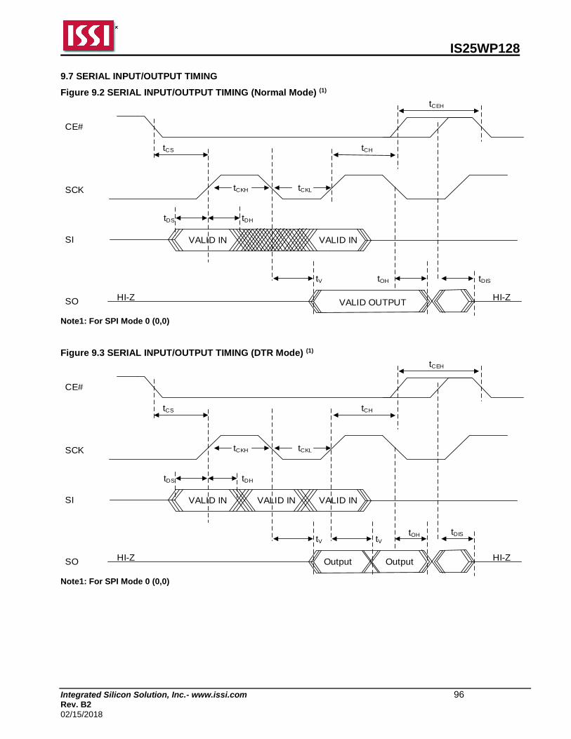
IS25WP128
Integrated Silicon Solution, Inc.- www.issi.com 96 Rev. B2
02/15/2018
9.7 SERIAL INPUT/OUTPUT TIMING
Figure 9.2 SERIAL INPUT/OUTPUT TIMING (Normal Mode) (1)
HI-ZSO
SI
SCK
CE#
VALID IN
tCS
tCKH tCKL
tDS tDH
tCH
tCEH
tV tDIS
HI-Z
tOH
VALID IN
VALID OUTPUT
Note1: For SPI Mode 0 (0,0)
Figure 9.3 SERIAL INPUT/OUTPUT TIMING (DTR Mode) (1)
HI-ZSO
SI
SCK
CE#
VALID IN
tCS
tCKH tCKL
tDS tDH
tCH
tCEH
tVtDIS
HI-Z
tOH
VALID INVALID IN
OutputOutput
tV
Note1: For SPI Mode 0 (0,0)
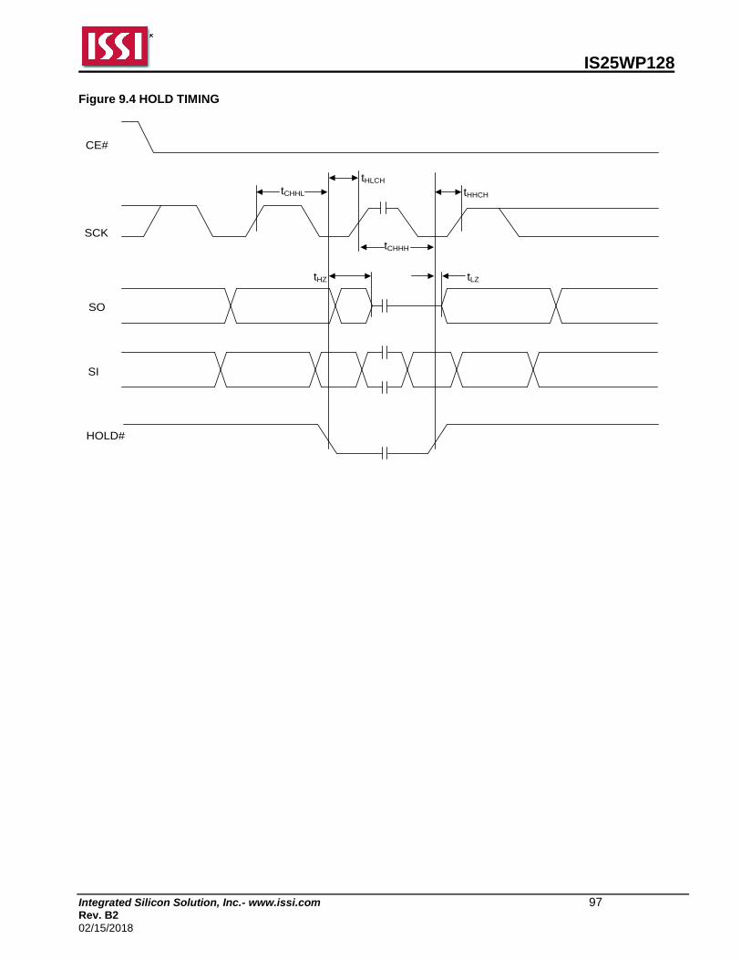
IS25WP128
Integrated Silicon Solution, Inc.- www.issi.com 97 Rev. B2
02/15/2018
Figure 9.4 HOLD TIMING
SI
SO
SCK
CE#
HOLD#
tCHHL
tHLCH
tCHHH
tHHCH
tHZ tLZ
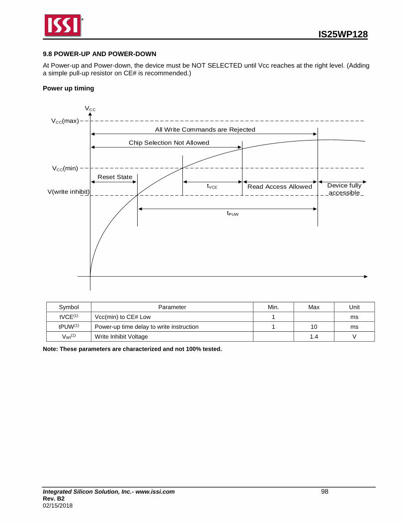
IS25WP128
Integrated Silicon Solution, Inc.- www.issi.com 98 Rev. B2
02/15/2018
9.8 POWER-UP AND POWER-DOWN
At Power-up and Power-down, the device must be NOT SELECTED until Vcc reaches at the right level. (Adding a simple pull-up resistor on CE# is recommended.) Power up timing
VCC
VCC(max)
VCC(min)
V(write inhibit)
Reset State
tVCE
tPUW
Read Access Allowed Device fully
accessible
Chip Selection Not Allowed
All Write Commands are Rejected
Symbol Parameter Min. Max Unit
tVCE(1) Vcc(min) to CE# Low 1 ms
tPUW(1) Power-up time delay to write instruction 1 10 ms
VWI(1) Write Inhibit Voltage 1.4 V
Note: These parameters are characterized and not 100% tested.
IS25WP128
Integrated Silicon Solution, Inc.- www.issi.com 99 Rev. B2
02/15/2018
9.9 PROGRAM/ERASE PERFORMANCE
Parameter Typ Max Unit
Sector Erase Time (4Kbyte) 70 300 ms
Block Erase Time (32Kbyte) 0.1 0.5 s
Block Erase Time (64Kbyte) 0.15 1.0 s
Chip Erase Time 30 90 s
Page Programming Time 0.2 0.8 ms
Byte Program 8 40 µs
Note: These parameters are characterized and not 100% tested.
9.10 RELIABILITY CHARACTERISTICS
Parameter Min Max Unit Test Method
Endurance 100,000 - Cycles JEDEC Standard A117
Data Retention 20 - Years JEDEC Standard A117
Latch-Up -100 +100 mA JEDEC Standard 78
Note: These parameters are characterized and not 100% tested.
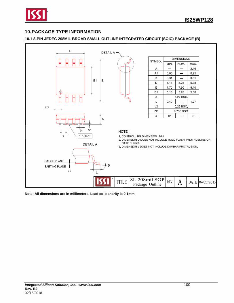
IS25WP128
Integrated Silicon Solution, Inc.- www.issi.com 100 Rev. B2
02/15/2018
10. PACKAGE TYPE INFORMATION
10.1 8-PIN JEDEC 208MIL BROAD SMALL OUTLINE INTEGRATED CIRCUIT (SOIC) PACKAGE (B)
Note: All dimensions are in millimeters. Lead co-planarity is 0.1mm.
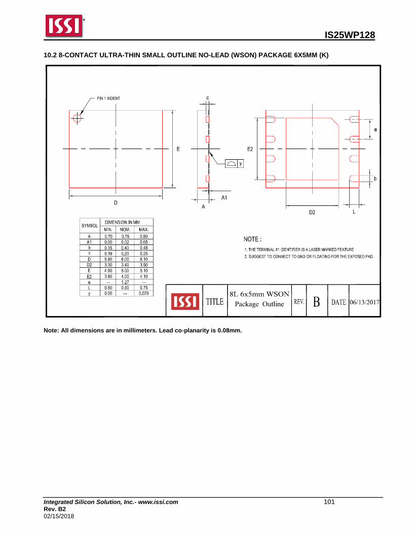
IS25WP128
Integrated Silicon Solution, Inc.- www.issi.com 101 Rev. B2
02/15/2018
10.2 8-CONTACT ULTRA-THIN SMALL OUTLINE NO-LEAD (WSON) PACKAGE 6X5MM (K)
Note: All dimensions are in millimeters. Lead co-planarity is 0.08mm.
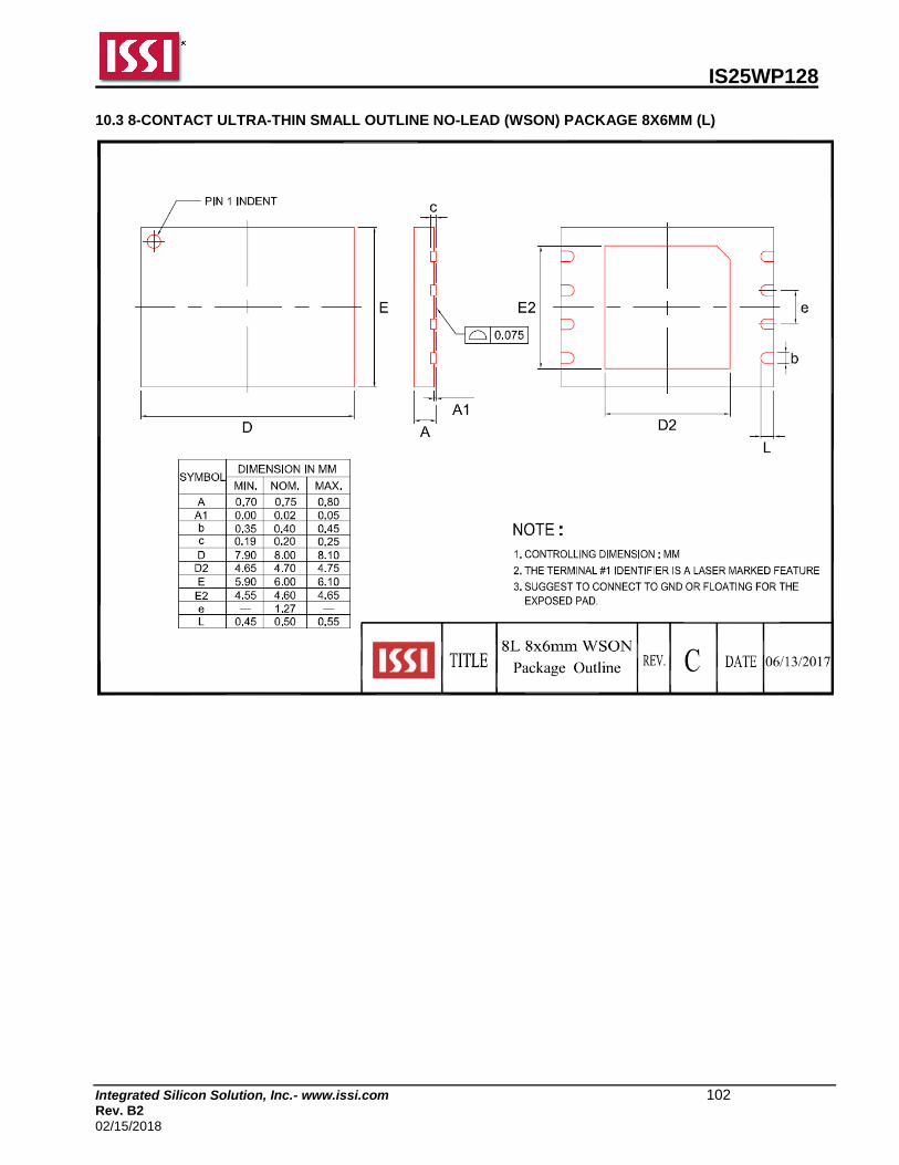
IS25WP128
Integrated Silicon Solution, Inc.- www.issi.com 102 Rev. B2
02/15/2018
10.3 8-CONTACT ULTRA-THIN SMALL OUTLINE NO-LEAD (WSON) PACKAGE 8X6MM (L)
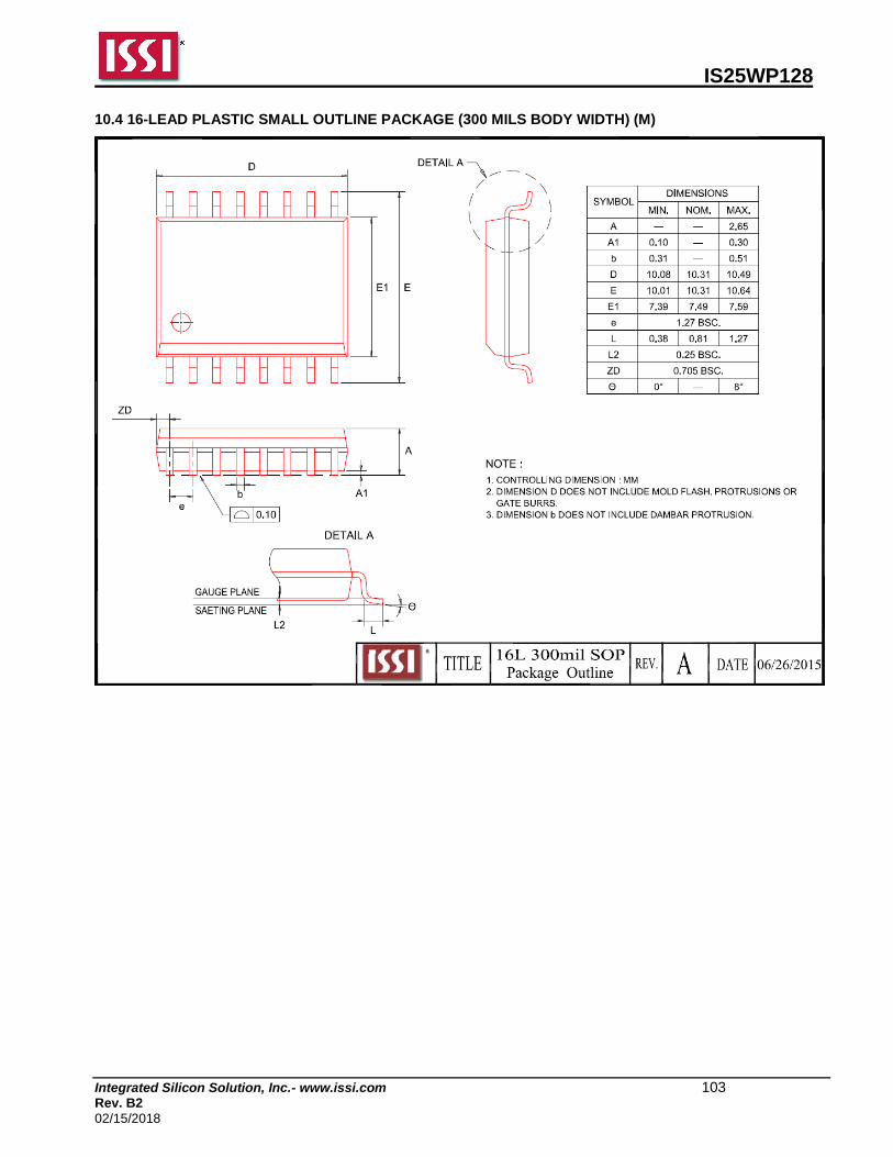
IS25WP128
Integrated Silicon Solution, Inc.- www.issi.com 103 Rev. B2
02/15/2018
10.4 16-LEAD PLASTIC SMALL OUTLINE PACKAGE (300 MILS BODY WIDTH) (M)
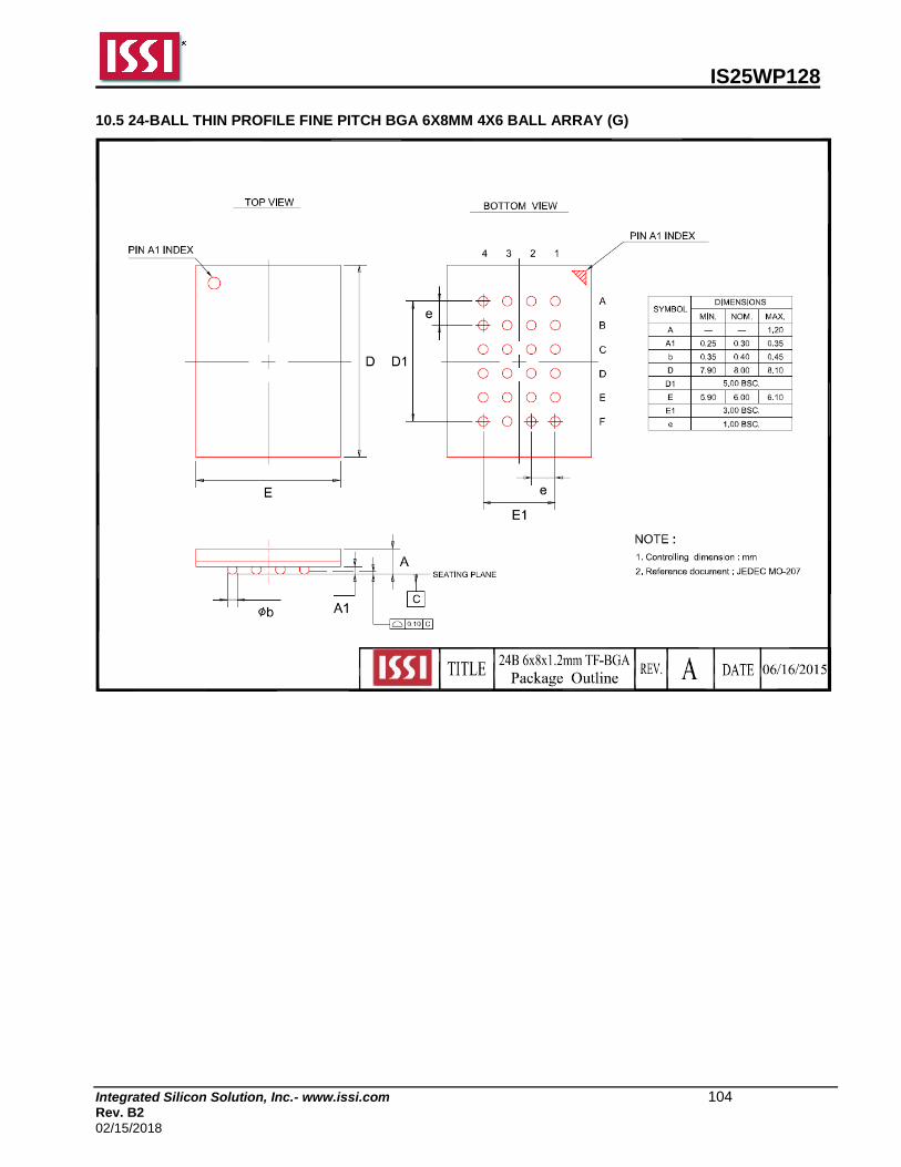
IS25WP128
Integrated Silicon Solution, Inc.- www.issi.com 104 Rev. B2
02/15/2018
10.5 24-BALL THIN PROFILE FINE PITCH BGA 6X8MM 4X6 BALL ARRAY (G)
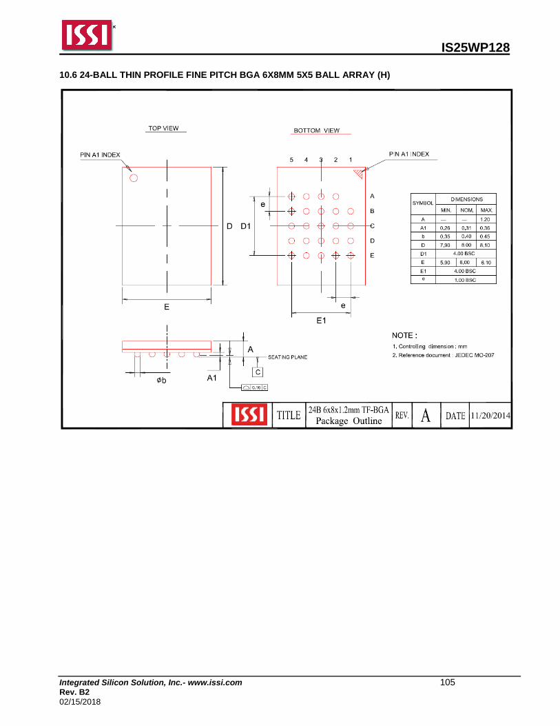
IS25WP128
Integrated Silicon Solution, Inc.- www.issi.com 105 Rev. B2
02/15/2018
10.6 24-BALL THIN PROFILE FINE PITCH BGA 6X8MM 5X5 BALL ARRAY (H)
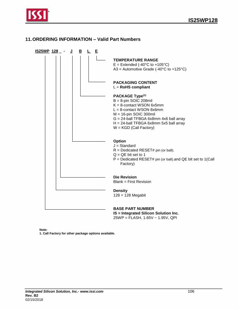
IS25WP128
Integrated Silicon Solution, Inc.- www.issi.com 106 Rev. B2
02/15/2018
11. ORDERING INFORMATION – Valid Part Numbers
IS25WP 128 - J B L E
TEMPERATURE RANGE E = Extended (-40°C to +105°C) A3 = Automotive Grade (-40°C to +125°C) PACKAGING CONTENT L = RoHS compliant PACKAGE Type(1) B = 8-pin SOIC 208mil K = 8-contact WSON 6x5mm L = 8-contact WSON 8x6mm M = 16-pin SOIC 300mil G = 24-ball TFBGA 6x8mm 4x6 ball array H = 24-ball TFBGA 6x8mm 5x5 ball array W = KGD (Call Factory) Option J = Standard R = Dedicated RESET# pin (or ball). Q = QE bit set to 1 P = Dedicated RESET# pin (or ball).and QE bit set to 1(Call
Factory) Die Revision Blank = First Revision Density 128 = 128 Megabit BASE PART NUMBER IS = Integrated Silicon Solution Inc. 25WP = FLASH, 1.65V ~ 1.95V, QPI
Note: 1. Call Factory for other package options available.
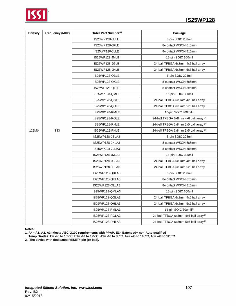
IS25WP128
Integrated Silicon Solution, Inc.- www.issi.com 107 Rev. B2
02/15/2018
Notes: 1. A* = A1, A2, A3: Meets AEC-Q100 requirements with PPAP, E1= Extended+ non-Auto qualified Temp Grades: E= -40 to 105°C, E1= -40 to 125°C, A1= -40 to 85°C, A2= -40 to 105°C, A3= -40 to 125°C 2. .The device with dedicated RESET# pin (or ball).
Density Frequency (MHz) Order Part Number(1) Package
128Mb 133
IS25WP128-JBLE 8-pin SOIC 208mil
IS25WP128-JKLE 8-contact WSON 6x5mm
IS25WP128-JLLE 8-contact WSON 8x6mm
IS25WP128-JMLE 16-pin SOIC 300mil
IS25WP128-JGLE 24-ball TFBGA 6x8mm 4x6 ball array
IS25WP128-JHLE 24-ball TFBGA 6x8mm 5x5 ball array
IS25WP128-QBLE 8-pin SOIC 208mil
IS25WP128-QKLE 8-contact WSON 6x5mm
IS25WP128-QLLE 8-contact WSON 8x6mm
IS25WP128-QMLE 16-pin SOIC 300mil
IS25WP128-QGLE 24-ball TFBGA 6x8mm 4x6 ball array
IS25WP128-QHLE 24-ball TFBGA 6x8mm 5x5 ball array
IS25WP128-RMLE 16-pin SOIC 300mil(2)
IS25WP128-RGLE 24-ball TFBGA 6x8mm 4x6 ball array (2)
IS25WP128-RHLE 24-ball TFBGA 6x8mm 5x5 ball array (2)
IS25WP128-PHLE 24-ball TFBGA 6x8mm 5x5 ball array (2)
IS25WP128-JBLA3 8-pin SOIC 208mil
IS25WP128-JKLA3 8-contact WSON 6x5mm
IS25WP128-JLLA3 8-contact WSON 8x6mm
IS25WP128-JMLA3 16-pin SOIC 300mil
IS25WP128-JGLA3 24-ball TFBGA 6x8mm 4x6 ball array
IS25WP128-JHLA3 24-ball TFBGA 6x8mm 5x5 ball array
IS25WP128-QBLA3 8-pin SOIC 208mil
IS25WP128-QKLA3 8-contact WSON 6x5mm
IS25WP128-QLLA3 8-contact WSON 8x6mm
IS25WP128-QMLA3 16-pin SOIC 300mil
IS25WP128-QGLA3 24-ball TFBGA 6x8mm 4x6 ball array
IS25WP128-QHLA3 24-ball TFBGA 6x8mm 5x5 ball array
IS25WP128-RMLA3 16-pin SOIC 300mil(2)
IS25WP128-RGLA3 24-ball TFBGA 6x8mm 4x6 ball array(2)
IS25WP128-RHLA3 24-ball TFBGA 6x8mm 5x5 ball array(2)