Embed Size (px)
Citation preview
IS25LP256 IS25WP256
256MBIT SERIAL FLASH MEMORY WITH 166MHZ MULTI I/O SPI & QUAD I/O QPI DTR INTERFACE
ADVANCED DATA SHEET

IS25LP256, IS25WP256
Integrated Silicon Solution, Inc.- www.issi.com 2 Rev.00A 05/14/2015
FEATURES
• Industry Standard Serial Interface - IS25LP256: 256Mbit/32Mbyte - IS25WP256: 256Mbit/32Mbyte - 3 or 4 Byte Addressing Mode - Supports Standard SPI, Fast, Dual, Dual
I/O, Quad, Quad I/O, SPI DTR, Dual I/O DTR, Quad I/O DTR, and QPI
- Software & Hardware Reset - Supports Serial Flash Discoverable
Parameters (SFDP)
• High Performance Serial Flash (SPI) - 80MHz Normal Read - Up to166Mhz Fast Read - Up to 80MHz DTR (Dual Transfer Rate) - Equivalent Throughput of 664 Mb/s - Selectable Dummy Cycles - Configurable Drive Strength - Supports SPI Modes 0 and 3 - More than 100,000 Erase/Program Cycles - More than 20-year Data Retention
• Flexible & Efficient Memory Architecture
- Chip Erase with Uniform Sector/Block Erase (4/32/64 Kbyte)
- Program 1 to 256 Byte per Page - Program/Erase Suspend & Resume
• Efficient Read and Program modes
- Low Instruction Overhead Operations - Continuous Read 8/16/32/64 Byte Burst - Selectable Burst Length - QPI for Reduced Instruction Overhead - AutoBoot Operation
• Low Power with Wide Temp. Ranges - Single Voltage Supply
IS25LP: 2.30V to 3.60V IS25WP: 1.65V to 1.95V
- 10 mA Active Read Current - 8 µA Standby Current - 1 µA Deep Power Down - Temp Grades:
Extended: -40°C to +105°C Extended+: -40°C to +125°C Auto Grade: up to +125°C
Note: Extended+ should not be used for Automotive.
• Advanced Security Protection - Software and Hardware Write Protection - Advanced Sector/Block Protection - Top/Bottom Block protection - Power Supply Lock Protection - 4x256 Byte Dedicated Security Area
with OTP User-lockable Bits - 128 bit Unique ID for Each Device
(Call Factory)
• Industry Standard Pin-out & Packages - M =16-pin SOIC 300mil - L = 8-contact WSON 8x6mm - G = 24-ball TFBGA 6x8mm (4x6 ball array)(1) - H = 24-ball TFBGA 6x8mm (5x5 ball array)(1) - KGD (Call Factory)
Note: For the additional RESET# pin option, call Factory
256MBIT SERIAL FLASH MEMORY WITH 166MHZ MULTI I/O SPI & QUAD I/O QPI DTR INTERFACE
ADVANCED INFORMATION

IS25LP256, IS25WP256
Integrated Silicon Solution, Inc.- www.issi.com 3 Rev.00A 05/14/2015
GENERAL DESCRIPTION The IS25LP256 and IS25WP256 Serial Flash memory offers a versatile storage solution with high flexibility and performance in a simplified pin count package. ISSI’s “Industry Standard Serial Interface” Flash is for systems that require limited space, a low pin count, and low power consumption. The device is accessed through a 4-wire SPI Interface consisting of a Serial Data Input (SI), Serial Data Output (SO), Serial Clock (SCK), and Chip Enable (CE#) pins, which can also be configured to serve as multi-I/O (see pin descriptions). The device supports Dual and Quad I/O as well as standard, Dual Output, and Quad Output SPI. Clock frequencies of up to 166MHz allow for equivalent clock rates of up to 664MHz (166MHz x 4) which equates to 83Mbytes/s of data throughput. The IS25xP series of Flash adds support for DTR (Double Transfer Rate) commands that transfer addresses and read data on both edges of the clock. These transfer rates can outperform 16-bit Parallel Flash memories allowing for efficient memory access to support XIP (execute in place) operation. The memory array is organized into programmable pages of 256 bytes. This family supports page program mode where 1 to 256 bytes of data are programmed in a single command. QPI (Quad Peripheral Interface) supports 2-cycle instruction further reducing instruction times. Pages can be erased in groups of 4Kbyte sectors, 32Kbyte blocks, 64Kbyte blocks, and/or the entire chip. The uniform sector and block architecture allows for a high degree of flexibility so that the device can be utilized for a broad variety of applications requiring solid data retention. GLOSSARY Standard SPI In this operation, a 4-wire SPI Interface is utilized, consisting of Serial Data Input (SI), Serial Data Output (SO), Serial Clock (SCK), and Chip Enable (CE#) pins. Instructions are sent via the SI pin to encode instructions, addresses, or input data to the device on the rising edge of SCK. The SO pin is used to read data or to check the status of the device. This device supports SPI bus operation modes (0,0) and (1,1). Mutil I/O SPI Multi-I/O operation utilizes an enhanced SPI protocol to allow the device to function with Dual Output, Dual Input and Output, Quad Output, and Quad Input and Output capability. Executing these instructions through SPI mode will achieve double or quadruple the transfer bandwidth for READ and PROGRAM operations. Quad I/O QPI The device enables QPI protocol by issuing an “Enter QPI mode (35h)” command. The QPI mode uses four IO pins for input and output to decrease SPI instruction overhead and increase output bandwidth. SI and SO pins become bidirectional IO0 and IO1, and WP# and HOLD# pins become IO2 and IO3 respectively during QPI mode. Issuing an “Exit QPI (F5h) command will cause the device to exit QPI mode. Power Reset or Hardware/Software Reset can also return the device into the standard SPI mode. DTR In addition to SPI and QPI features, the device also supports SPI DTR READ. SPI DTR allows high data throughput while running at lower clock frequencies. SPI DTR READ mode uses both rising and falling edges of the clock to drive output, resulting in reducing input and output cycles by half. Programmable drive strength and Selectable burst setting. The device offers programmable output drive strength and selectable burst (wrap) length features to increase the efficiency and performance of READ operation. The driver strength and burst setting features are controlled by setting the Read Registers. A total of six different drive strengths and four different burst sizes (8/16/32/64 Byte) are available for selection.
IS25LP256, IS25WP256
Integrated Silicon Solution, Inc.- www.issi.com 4 Rev.00A 05/14/2015
TABLE OF CONTENTS
FEATURES .......................................................................................................................................................... 2 GENERAL DESCRIPTION .................................................................................................................................. 3 TABLE OF CONTENTS ....................................................................................................................................... 4 1. PIN CONFIGURATION ................................................................................................................................. 7 2. PIN DESCRIPTIONS .................................................................................................................................... 9 3. BLOCK DIAGRAM ...................................................................................................................................... 11 4. SPI MODES DESCRIPTION ...................................................................................................................... 12 5. SYSTEM CONFIGURATION ...................................................................................................................... 14
5.1 BLOCK/SECTOR ADDRESSES .......................................................................................................... 14 6. REGISTERS ............................................................................................................................................... 15
6.1 STATUS REGISTER ............................................................................................................................ 15 6.2 FUNCTION REGISTER ........................................................................................................................ 18 6.3 READ REGISTER AND EXTENDED REGISTER ................................................................................ 19
6.3.1 READ REGISTER ........................................................................................................................ 19 6.3.2 EXTENDED READ REGISTER .................................................................................................... 21
6.4 AUTOBOOT REGISTER ...................................................................................................................... 23 6.5 BANK ADDRESS REGISTER .............................................................................................................. 23 6.6 ADVANCED SECTOR/BLOCK PROTECTION (ASP) RELATED REGISTER .................................... 24
6.6.1 ADVANCED SECTOR/BLOCK PROTECTION REGISTER (ASPR) ........................................... 24 6.6.2 PASSWORD REGISTER ............................................................................................................. 25 6.6.3 PPB LOCK REGISTER ................................................................................................................ 25 6.6.4 PPB REGISTER ........................................................................................................................... 26 6.6.5 DYB REGISTER ........................................................................................................................... 26
7. PROTECTION MODE................................................................................................................................. 27 7.1 HARDWARE WRITE PROTECTION.................................................................................................... 27 7.2 SOFTWARE WRITE PROTECTION .................................................................................................... 27
7.2.1 BLOCK PROTECTION BITS ........................................................................................................ 27
7.2.2 ADVANCED SECTOR/BLOCK PROTECTION (ASP) ................................................................. 28 8. DEVICE OPERATION ................................................................................................................................ 35
8.1 COMMAND OVERVIEW ...................................................................................................................... 35 8.2 COMMAND SET SUMMARY ............................................................................................................... 36 8.3 NORMAL READ OPERATION (NORD, 03h or 4NORD, 13h) ............................................................. 45 8.4 FAST READ OPERATION (FRD, 0Bh or 4FRD, 0Ch) ......................................................................... 48 8.5 HOLD OPERATION .............................................................................................................................. 52 8.6 FAST READ DUAL I/O OPERATION (FRDIO, BBh or 4FRDIO, BCh) ................................................ 53 8.7 FAST READ DUAL OUTPUT OPERATION (FRDO, 3Bh or 4FRDO, 3Ch)......................................... 57 8.8 FAST READ QUAD OUTPUT OPERATION (FRQO, 6Bh or 4FRQO 6Ch) ........................................ 60 8.9 FAST READ QUAD I/O OPERATION (FRQIO, EBh or 4FRQIO, ECh) ............................................... 63

IS25LP256, IS25WP256
Integrated Silicon Solution, Inc.- www.issi.com 5 Rev.00A 05/14/2015
8.10 PAGE PROGRAM OPERATION (PP, 02h or 4PP, 12h).................................................................... 70 8.11 QUAD INPUT PAGE PROGRAM OPERATION (PPQ, 32h/38h or 4PPQ, 34h/3Eh) ........................ 73 8.12 ERASE OPERATION ......................................................................................................................... 74 8.13 SECTOR ERASE OPERATION (SER, D7h/20h or 4SER, 21h) ........................................................ 75 8.14 BLOCK ERASE OPERATION (BER32K:52h or 4BER32K:5Ch, BER64K:D8h or 4BER64K:DCh) .. 77 8.15 CHIP ERASE OPERATION (CER, C7h/60h) ..................................................................................... 80 8.16 WRITE ENABLE OPERATION (WREN, 06h) .................................................................................... 81 8.17 WRITE DISABLE OPERATION (WRDI, 04h) ..................................................................................... 82 8.18 READ STATUS REGISTER OPERATION (RDSR, 05h) ................................................................... 83 8.19 WRITE STATUS REGISTER OPERATION (WRSR, 01h) ................................................................. 84 8.20 READ FUNCTION REGISTER OPERATION (RDFR, 48h) ............................................................... 85 8.21 WRITE FUNCTION REGISTER OPERATION (WRFR, 42h)............................................................. 86 8.22 ENTER QUAD PERIPHERAL INTERFACE (QPI) MODE OPERATION (QIOEN,35h; QIODI,F5h) . 87 8.23 PROGRAM/ERASE SUSPEND & RESUME ...................................................................................... 88 8.24 ENTER DEEP POWER DOWN (DP, B9h) ......................................................................................... 91 8.25 RELEASE DEEP POWER DOWN (RDPD, ABh) ............................................................................... 92 8.26 SET READ PARAMETERS OPERATION (SRPNV: 65h, SRPV: C0h/63h) ...................................... 93 8.27 SET EXTENDED READ PARAMETERS OPERATION (SERPNV: 85h, SERPV: 83h) .................... 95 8.28 READ READ PARAMETERS OPERATION (RDRP, 61h) ................................................................. 96 8.29 READ EXTENDED READ PARAMETERS OPERATION (RDERP, 81h) .......................................... 97 8.30 CLEAR EXTENDED READ REGISTER OPERATION (CLERP, 82h) ............................................... 98 8.31 READ PRODUCT IDENTIFICATION (RDID, ABh) ............................................................................ 99 8.32 READ PRODUCT IDENTIFICATION BY JEDEC ID OPERATION (RDJDID, 9Fh; RDJDIDQ, AFh) .................................................................................................................................................................. 101 8.33 READ DEVICE MANUFACTURER AND DEVICE ID OPERATION (RDMDID, 90h) ...................... 102 8.34 READ UNIQUE ID NUMBER (RDUID, 4Bh) .................................................................................... 103 8.35 READ SFDP OPERATION (RDSFDP, 5Ah) .................................................................................... 104 8.36 NO OPERATION (NOP, 00h) ........................................................................................................... 104 8.37 SOFTWARE RESET (RESET-ENABLE (RSTEN, 66h) AND RESET (RST, 99h)) AND HARDWARE RESET ...................................................................................................................................................... 105 8.38 SECURITY INFORMATION ROW .................................................................................................... 106 8.39 INFORMATION ROW ERASE OPERATION (IRER, 64h) ............................................................... 107 8.40 INFORMATION ROW PROGRAM OPERATION (IRP, 62h) ........................................................... 108 8.41 INFORMATION ROW READ OPERATION (IRRD, 68h) ................................................................. 109 8.42 FAST READ DTR MODE OPERATION (FRDTR, 0Dh or 4FRDTR, 0Eh) ....................................... 110 8.43 FAST READ DUAL IO DTR MODE OPERATION (FRDDTR, BDh or 4FRDDTR, BEh) ................. 115 8.44 FAST READ QUAD IO DTR MODE OPERATION (FRQDTR, EDh or 4FRQDTR, EEh) ................ 119 8.45 SECTOR LOCK/UNLOCK FUNCTIONS .......................................................................................... 127 8.46 AUTOBOOT ...................................................................................................................................... 130 8.47 READ BANK ADDRESS REGISTER OPERATION (RDBR: 16h/C8h) ........................................... 134

IS25LP256, IS25WP256
Integrated Silicon Solution, Inc.- www.issi.com 6 Rev.00A 05/14/2015
8.48 WRITE BANK ADDRESS REGISTER OPERATION (WRBRNV: 18h, WRBRV: 17h/C5h) ............ 135 8.49 ENTER 4-BYTE ADDRESS MODE OPERATION (EN4B, B7h) ...................................................... 136 8.50 EXIT 4-BYTE ADDRESS MODE OPERATION (EX4B, 29h) ........................................................... 137 8.51 READ DYB OPERATION (RDDYB, FAh or 4RDDYB, E0h) ............................................................ 138 8.52 WRITE DYB OPERATION (WRDYB, FBh or 4WRDYB, E1h) ......................................................... 140 8.53 READ PPB OPERATION (RDPPB, FCh or 4RDPPB, E2h) ............................................................ 142 8.54 PROGRAM PPB OPERATION (PGPPB, FDh or 4PGPPB, E3h) .................................................... 143 8.55 ERASE PPB OPERATION (ERPPB, E4h) ....................................................................................... 145 8.56 READ ASP OPERATION (RDASP, 2Bh) ......................................................................................... 146 8.57 PROGRAM ASP OPERATION (PGASP, 2Fh) ................................................................................. 147 8.58 READ PPB LOCK BIT OPERATION (RDPLB, A7h) ........................................................................ 148 8.59 WRITE PPB LOCK BIT OPERATION (WRPLB, A6h) ...................................................................... 149 8.60 SET FREEZE BIT OPERATION (SFRZ, 91h) .................................................................................. 150 8.61 READ PASSWORD OPERATION (RDPWD, E7h) .......................................................................... 151 8.62 PROGRAM PASSWORD OPERATION (PGPWD, E8h) ................................................................. 152 8.63 UNLOCK PASSWORD OPERATION (UNPWD, E9h) ..................................................................... 153 8.64 GANG SECTOR/BLOCK LOCK OPERATION (GBLK, 7Eh) ........................................................... 154 8.65 GANG SECTOR/BLOCK UNLOCK OPERATION (GBUN, 98h) ...................................................... 155
9. ELECTRICAL CHARACTERISTICS ......................................................................................................... 156 9.1 ABSOLUTE MAXIMUM RATINGS (1) ................................................................................................. 156 9.2 OPERATING RANGE ......................................................................................................................... 156 9.3 DC CHARACTERISTICS .................................................................................................................... 157 9.4 AC MEASUREMENT CONDITIONS .................................................................................................. 158 9.5 AC CHARACTERISTICS .................................................................................................................... 159 9.6 SERIAL INPUT/OUTPUT TIMING ...................................................................................................... 161 9.7 POWER-UP AND POWER-DOWN .................................................................................................... 163 9.8 PROGRAM/ERASE PERFORMANCE ............................................................................................... 164 9.9 RELIABILITY CHARACTERISTICS ................................................................................................... 164
10. PACKAGE TYPE INFORMATION ....................................................................................................... 165 10.1 8-CONTACT ULTRA-THIN SMALL OUTLINE NO-LEAD (WSON) PACKAGE 8x6mm (L) ............. 165 10.2 16-LEAD PLASTIC SMALL OUTLINE PACKAGE (300 MILS BODY WIDTH) (M) .......................... 166 10.3 24-BALL THIN PROFILE FINE PITCH BGA 6x8mm 4x6 BALL ARRAY (G) ................................... 167 10.4 24- BALL THIN PROFILE FINE PITCH BGA 6x8mm 5x5 BALL ARRAY (H) .................................. 168
11. ORDERING INFORMATION – Valid Part Numbers ............................................................................ 169
IS25LP256, IS25WP256
Integrated Silicon Solution, Inc.- www.issi.com 7 Rev.00A 05/14/2015
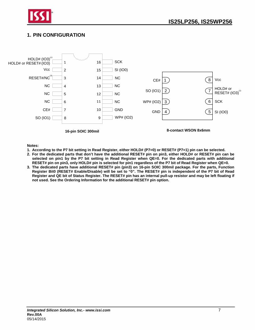
1. PIN CONFIGURATION
Notes: 1. According to the P7 bit setting in Read Register, either HOLD# (P7=0) or RESET# (P7=1) pin can be selected. 2. For the dedicated parts that don’t have the additional RESET# pin on pin3, either HOLD# or RESET# pin can be
selected on pin1 by the P7 bit setting in Read Register when QE=0. For the dedicated parts with additional RESET# pin on pin3, only HOLD# pin is selected for pin1 regardless of the P7 bit of Read Register when QE=0.
3. The dedicated parts have additional RESET# pin (pin3) on 16-pin SOIC 300mil package. For the parts, Function Register Bit0 (RESET# Enable/Disable) will be set to “0”. The RESET# pin is independent of the P7 bit of Read Register and QE bit of Status Register. The RESET# pin has an internal pull-up resistor and may be left floating if not used. See the Ordering Information for the additional RESET# pin option.
16-pin SOIC 300mil
(1)
(3)
(2)
6 3
CE# Vcc
SCK
SI (IO0)
7
8
5 4
1
2
GND
WP# (IO2)
SO (IO1) HOLD# or RESET# (IO3)
8-contact WSON 8x6mm
12
10
11
9
13
15
14
5
7
6
8
4
2
3
16 1
Vcc
HOLD# (IO3) HOLD# or RESET# (IO3) SCK
CE#
WP# (IO2)
GND
NC
NC
NC
NC
NC
SI (IO0)
SO (IO1)
NC
NC
RESET#/NC
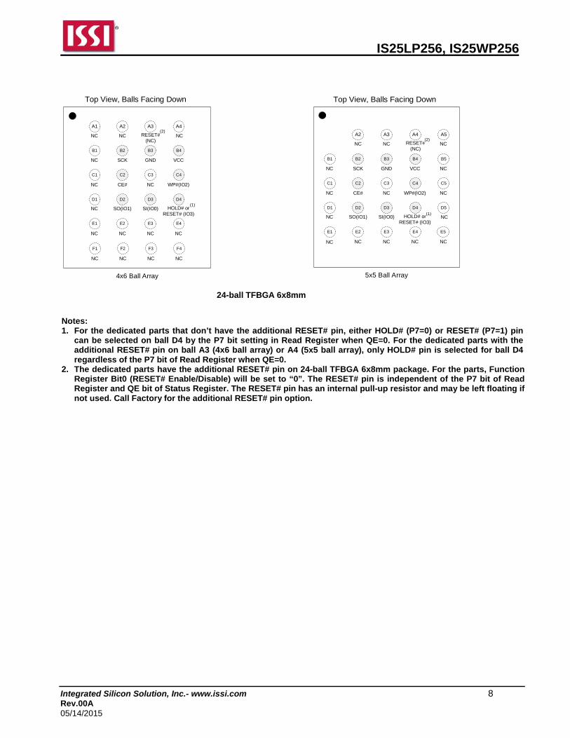
IS25LP256, IS25WP256
Integrated Silicon Solution, Inc.- www.issi.com 8 Rev.00A 05/14/2015
Top View, Balls Facing Down
4x6 Ball Array
NC NC NC NC
F1 F2 F3 F4
NC RESET#(NC)
NC
NC SCK GND VCC
NC CE# NC WP#(IO2)
NC SO(IO1) SI(IO0) HOLD# or RESET# (IO3)
NC NC NC NC
NC
A2 A3 A4
B1 B2 B3 B4
C1 C2 C3 C4
D1 D2 D3 D4
E1 E2 E3 E4
A1
NC NC RESET#(NC)
NC SCK GND VCC
NC CE# NC WP#(IO2)
NC SO(IO1) SI(IO0) HOLD# or RESET# (IO3)
NC NC NC NC
NC
NC
NC
NC
Top View, Balls Facing Down
NC
5x5 Ball Array
A2 A3 A4
B1 B2 B3 B4
C1 C2 C3 C4
D1 D2 D3 D4
E1 E2 E3 E4
A5
B5
C5
D5
E5
Notes: 1. For the dedicated parts that don’t have the additional RESET# pin, either HOLD# (P7=0) or RESET# (P7=1) pin
can be selected on ball D4 by the P7 bit setting in Read Register when QE=0. For the dedicated parts with the additional RESET# pin on ball A3 (4x6 ball array) or A4 (5x5 ball array), only HOLD# pin is selected for ball D4 regardless of the P7 bit of Read Register when QE=0.
2. The dedicated parts have the additional RESET# pin on 24-ball TFBGA 6x8mm package. For the parts, Function Register Bit0 (RESET# Enable/Disable) will be set to “0”. The RESET# pin is independent of the P7 bit of Read Register and QE bit of Status Register. The RESET# pin has an internal pull-up resistor and may be left floating if not used. Call Factory for the additional RESET# pin option.
24-ball TFBGA 6x8mm
(2)
(1) (1)
(2)

IS25LP256, IS25WP256
Integrated Silicon Solution, Inc.- www.issi.com 9 Rev.00A 05/14/2015
2. PIN DESCRIPTIONS
For all other packages except the package with additional RESET# pin option
SYMBOL TYPE DESCRIPTION
CE# INPUT
Chip Enable: The Chip Enable (CE#) pin enables and disables the devices operation. When CE# is high the device is deselected and output pins are in a high impedance state. When deselected the devices non-critical internal circuitry power down to allow minimal levels of power consumption while in a standby state.
When CE# is pulled low the device will be selected and brought out of standby mode. The device is considered active and instructions can be written to, data read, and written to the device. After power-up, CE# must transition from high to low before a new instruction will be accepted.
Keeping CE# in a high state deselects the device and switches it into its low power state. Data will not be accepted when CE# is high.
SI (IO0), SO (IO1)
INPUT/ OUTPUT
Serial Data Input, Serial Output, and IOs (SI, SO, IO0, and IO1): This device supports standard SPI, Dual SPI, and Quad SPI operation. Standard SPI instructions use the unidirectional SI (Serial Input) pin to write instructions, addresses, or data to the device on the rising edge of the Serial Clock (SCK). Standard SPI also uses the unidirectional SO (Serial Output) to read data or status from the device on the falling edge of the serial clock (SCK).
In Dual and Quad SPI mode, SI and SO become bidirectional IO pins to write instructions, addresses or data to the device on the rising edge of the Serial Clock (SCK) and read data or status from the device on the falling edge of SCK. Quad SPI instructions use the WP# and HOLD# pins as IO2 and IO3 respectively.
WP# (IO2) INPUT/ OUTPUT
Write Protect/Serial Data IO (IO2): The WP# pin protects the Status Register from being written in conjunction with the SRWD bit. When the SRWD is set to “1” and the WP# is pulled low, the Status Register bits (SRWD, QE, BP3, BP2, BP1, BP0) are write-protected and vice-versa for WP# high. When the SRWD is set to “0”, the Status Register is not write-protected regardless of WP# state.
When the QE bit is set to “1”, the WP# pin (Write Protect) function is not available since this pin is used for IO2.
HOLD# or RESET# (IO3)
INPUT/ OUTPUT
HOLD# or RESET#/Serial Data IO (IO3): When the QE bit of Status Register is set to “1”, HOLD# pin or RESET# is not available since it becomes IO3. When QE=0 the pin acts as HOLD# or RESET# and either one can be selected by the P7 bit setting in Read Register. HOLD# will be selected if P7=0 (Default) and RESET# will be selected if P7=1.
The HOLD# pin allows the device to be paused while it is selected. It pauses serial communication by the master device without resetting the serial sequence. The HOLD# pin is active low. When HOLD# is in a low state and CE# is low, the SO pin will be at high impedance. Device operation can resume when HOLD# pin is brought to a high state.
RESET# pin is a hardware RESET signal. When RESET# is driven HIGH, the memory is in the normal operating mode. When RESET# is driven LOW, the memory enters reset mode and output is High-Z. If RESET# is driven LOW while an internal WRITE, PROGRAM, or ERASE operation is in progress, data may be lost.
SCK INPUT Serial Data Clock: Synchronized Clock for input and output timing operations.
Vcc POWER Power: Device Core Power Supply
GND GROUND Ground: Connect to ground when referenced to Vcc
NC Unused NC: Pins labeled “NC” stand for “No Connect” and should be left uncommitted.
IS25LP256, IS25WP256
Integrated Silicon Solution, Inc.- www.issi.com 10 Rev.00A 05/14/2015
For the package with additional RESET# pin option - RESET# pin will be added to another pin without sharing with HOLD# pin (Call Factory for 24-ball TFBGA
6x8mm packages)
SYMBOL TYPE DESCRIPTION
CE# INPUT Same as the description in previous page
SI (IO0), SO (IO1)
INPUT/ OUTPUT
Same as the description in previous page
WP# (IO2) INPUT/ OUTPUT
Same as the description in previous page
HOLD# (IO3) INPUT/ OUTPUT
HOLD#/Serial Data IO (IO3): When the QE bit of Status Register is set to “1”, HOLD# pin is not available since it becomes IO3. When QE=0 the pin acts as HOLD# regardless of the P7 bit of Read Register.
The HOLD# pin allows the device to be paused while it is selected. It pauses serial communication by the master device without resetting the serial sequence. The HOLD# pin is active low. When HOLD# is in a low state and CE# is low, the SO pin will be at high impedance. Device operation can resume when HOLD# pin is brought to a high state.
RESET# INPUT
RESET#: This pin is available only for dedicated parts (Call Factory for 24-ball TFBGA 6x8mm packages).
The RESET# pin is a hardware RESET signal. When RESET# is driven HIGH, the memory is in the normal operating mode. When RESET# is driven LOW, the memory enters reset mode and output is High-Z. If RESET# is driven LOW while an internal WRITE, PROGRAM, or ERASE operation is in progress, data may be lost.
SCK INPUT Same as the description in previous page
Vcc POWER Same as the description in previous page
GND GROUND Same as the description in previous page
NC Unused Same as the description in previous page

IS25LP256, IS25WP256
Integrated Silicon Solution, Inc.- www.issi.com 11 Rev.00A 05/14/2015
3. BLOCK DIAGRAM
Note1: RESET# pin can be added to another pin without sharing with HOLD# pin for the dedicated parts. Call
Factory for the additional RESET# pin option for 24-ball TFBGA 6x8mm packages.
Control Logic High Voltage Generator
I/O Buffers and Data Latches
256 BytesPage Buffer
Y-Decoder
X-D
eco
der
Se
rial P
erip
her
al I
nte
rfa
ce
StatusRegister
Address Latch & Counter
Memory Array
CE#
SCK
WP#(IO2)
SI(IO0)
SO(IO1)
HOLD# or RESET# (IO3)
(1)

IS25LP256, IS25WP256
Integrated Silicon Solution, Inc.- www.issi.com 12 Rev.00A 05/14/2015
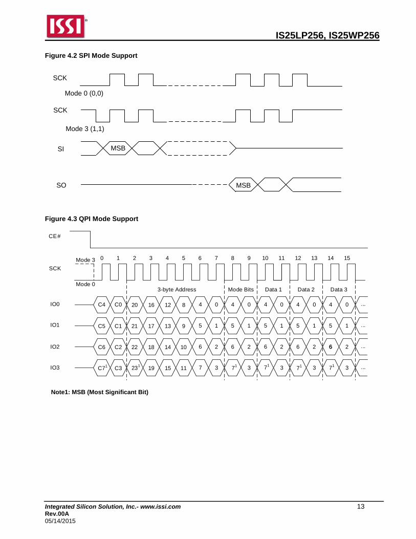
4. SPI MODES DESCRIPTION
Multiple IS25LP256 devices or multiple IS25WP256 devices can be connected on the SPI serial bus and controlled by a SPI Master, i.e. microcontroller, as shown in Figure 4.1. The devices support either of two SPI modes:
Mode 0 (0, 0) Mode 3 (1, 1)
The difference between these two modes is the clock polarity. When the SPI master is in stand-by mode, the serial clock remains at “0” (SCK = 0) for Mode 0 and the clock remains at “1” (SCK = 1) for Mode 3. Please refer to Figure 4.2 and Figure 4.3 for SPI and QPI mode. In both modes, the input data is latched on the rising edge of Serial Clock (SCK), and the output data is available from the falling edge of SCK. Figure 4.1 Connection Diagram among SPI Master and SPI Slaves (Memory Devices)
Notes: 1. RESET# pin can be added to another pin without sharing with HOLD# pin for the dedicated parts. Call Factory for
the additional RESET# pin option for 24-ball TFBGA 6x8mm packages. 2. SI and SO pins become bidirectional IO0 and IO1, and WP# and HOLD# pins become IO2 and IO3 respectively
during QPI mode.
SPI interface with(0,0) or (1,1)
SPI Master(i.e. Microcontroller)
SPIMemoryDevice
SPIMemoryDevice
SPIMemoryDevice
SCK SO SI
SCK
SDI
SDO
CE#
WP# HOLD# or RESET
SCK SO SI
CE#
WP# HOLD# or RESET#
SCK SO SI
CE#
WP#
CS3 CS2 CS1
HOLD# or RESET#
(1) (1) (1)
IS25LP256, IS25WP256
Integrated Silicon Solution, Inc.- www.issi.com 13 Rev.00A 05/14/2015
Figure 4.2 SPI Mode Support
SCK
SO
SI
Mode 0 (0,0)
Mode 3 (1,1)
MSB
MSB
SCK
Figure 4.3 QPI Mode Support
20
CE#
SCK
4 0 4 0
3-byte Address
16 12 8
0 1 2 3 4 5 6 7 8 9 10 11 12 13 14 15Mode 3
Mode 0
IO0
IO1 21 5 1 5 117 13 9
22 6 2 6 218 14 10
7 3 319 15 11
Mode Bits
IO2
IO3
C4 C0
C1C5
C2C6
C3C71
4 0 4 0
5 1 5 1
6 2 6 2
3 3
4
5
6
0
1
2
3
...
...
...
...
Data 1 Data 2 Data 3
231 71 7171 71
6
Note1: MSB (Most Significant Bit)

IS25LP256, IS25WP256
Integrated Silicon Solution, Inc.- www.issi.com 14 Rev.00A 05/14/2015
5. SYSTEM CONFIGURATION
The memory array is divided into uniform 4 Kbyte sectors or uniform 32/64 Kbyte blocks (a block consists of eight/sixteen adjacent sectors respectively). Table 5.1 illustrates the memory map of the device. The Status Register controls how the memory is protected.
5.1 BLOCK/SECTOR ADDRESSES
Table 5.1 Block/Sector Addresses of IS25LP256 and IS25WP256
Memory Density
Block No. (64Kbyte)
Block No. (32Kbyte) Sector No. Sector Size
(Kbyte) Address Range
256Mb
Block 0
Block 0 Sector 0 4 000000h - 000FFFh
: : :
Block 1 : : :
Sector 15 4 00F000h - 00FFFFh
Block 1
Block 2 Sector 16 4 010000h - 010FFFh
: : :
Block 3 : : :
Sector 31 4 01F000h - 01FFFFh
Block 2
Block 4 Sector 32 4 020000h - 020FFFh
: : :
Block 5 : : :
Sector 47 4 02F000h - 02FFFFh
: : : : :
Block 254
Block 508 Sector 4064 4 FE0000h – FE0FFFh
: : :
Block 509 : : :
Sector 4079 4 FEF000h – FEFFFFh
Block 255
Block 510 Sector 4080 4 FF0000h – FF0FFFh
: : :
Block 511 : : :
Sector 4095 4 FFF000h – FFFFFFh
: : : : :
Block 510
Block 1020 Sector 8160 4 1FE0000h – 1FE0FFFh
: : :
Block 1021 : : :
Sector 8175 4 1FEF000h – 1FEFFFFh
Block 511
Block 1022 Sector 8176 4 1FF0000h – 1FF0FFFh
: : :
Block 1023 : : :
Sector 8191 4 1FFF000h – 1FFFFFFh
IS25LP256, IS25WP256
Integrated Silicon Solution, Inc.- www.issi.com 15 Rev.00A 05/14/2015
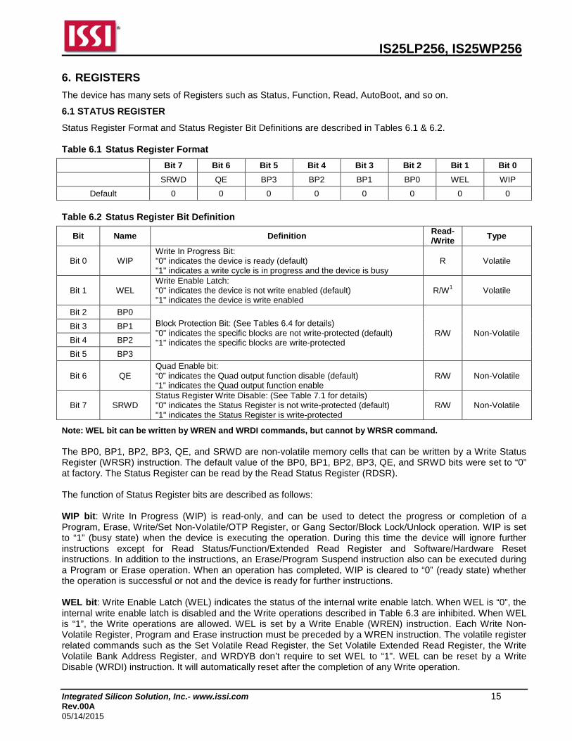
6. REGISTERS
The device has many sets of Registers such as Status, Function, Read, AutoBoot, and so on.
6.1 STATUS REGISTER
Status Register Format and Status Register Bit Definitions are described in Tables 6.1 & 6.2. Table 6.1 Status Register Format
Bit 7 Bit 6 Bit 5 Bit 4 Bit 3 Bit 2 Bit 1 Bit 0
SRWD QE BP3 BP2 BP1 BP0 WEL WIP
Default 0 0 0 0 0 0 0 0
Table 6.2 Status Register Bit Definition
Bit Name Definition Read- /Write Type
Bit 0 WIP Write In Progress Bit: "0" indicates the device is ready (default) "1" indicates a write cycle is in progress and the device is busy
R Volatile
Bit 1 WEL Write Enable Latch: "0" indicates the device is not write enabled (default) "1" indicates the device is write enabled
R/W1 Volatile
Bit 2 BP0 Block Protection Bit: (See Tables 6.4 for details) "0" indicates the specific blocks are not write-protected (default) "1" indicates the specific blocks are write-protected
R/W Non-Volatile Bit 3 BP1
Bit 4 BP2
Bit 5 BP3
Bit 6 QE Quad Enable bit: “0” indicates the Quad output function disable (default) “1” indicates the Quad output function enable
R/W Non-Volatile
Bit 7 SRWD Status Register Write Disable: (See Table 7.1 for details) "0" indicates the Status Register is not write-protected (default) "1" indicates the Status Register is write-protected
R/W Non-Volatile
Note: WEL bit can be written by WREN and WRDI commands, but cannot by WRSR command. The BP0, BP1, BP2, BP3, QE, and SRWD are non-volatile memory cells that can be written by a Write Status Register (WRSR) instruction. The default value of the BP0, BP1, BP2, BP3, QE, and SRWD bits were set to “0” at factory. The Status Register can be read by the Read Status Register (RDSR). The function of Status Register bits are described as follows: WIP bit: Write In Progress (WIP) is read-only, and can be used to detect the progress or completion of a Program, Erase, Write/Set Non-Volatile/OTP Register, or Gang Sector/Block Lock/Unlock operation. WIP is set to “1” (busy state) when the device is executing the operation. During this time the device will ignore further instructions except for Read Status/Function/Extended Read Register and Software/Hardware Reset instructions. In addition to the instructions, an Erase/Program Suspend instruction also can be executed during a Program or Erase operation. When an operation has completed, WIP is cleared to “0” (ready state) whether the operation is successful or not and the device is ready for further instructions. WEL bit: Write Enable Latch (WEL) indicates the status of the internal write enable latch. When WEL is “0”, the internal write enable latch is disabled and the Write operations described in Table 6.3 are inhibited. When WEL is “1”, the Write operations are allowed. WEL is set by a Write Enable (WREN) instruction. Each Write Non-Volatile Register, Program and Erase instruction must be preceded by a WREN instruction. The volatile register related commands such as the Set Volatile Read Register, the Set Volatile Extended Read Register, the Write Volatile Bank Address Register, and WRDYB don’t require to set WEL to “1". WEL can be reset by a Write Disable (WRDI) instruction. It will automatically reset after the completion of any Write operation.

IS25LP256, IS25WP256
Integrated Silicon Solution, Inc.- www.issi.com 16 Rev.00A 05/14/2015
Table 6.3 Instructions requiring WREN instruction ahead
Instructions must be preceded by the WREN instruction
Name Hex Code Operation
PP 02h Serial Input Page Program (3-byte or 4-byte Address)
4PP 12h Serial Input Page Program (4-byte Address)
PPQ 32h/38h Quad Input Page Program (3-byte or 4-byte Address)
4PPQ 34h/3Eh Quad Input Page Program (4-byte Address)
SER D7h/20h Sector Erase 4KB (3-byte or 4-byte Address)
4SER 21h Sector Erase 4KB (4-byte Address)
BER32 (32KB) 52h Block Erase 32KB (3-byte or 4-byte Address)
4BER32 (32KB) 5Ch Block Erase 32KB (4-byte Address)
BER64 (64KB) D8h Block Erase 64KB (3-byte or 4-byte Address)
4BER64 (64KB) DCh Block Erase 64KB (4-byte Address)
CER C7h/60h Chip Erase
WRSR 01h Write Status Register
WRFR 42h Write Function Register
SRPNV 65h Set Read Parameters (Non-Volatile)
SERPNV 85h Set Extended Read Parameters (Non-Volatile)
IRER 64h Erase Information Row
IRP 62h Program Information Row
WRABR 15h Write AutoBoot Register
WRBRNV 17h Write Non-Volatile Bank Address Register
PGPPB FDh Write PPB (3-byte or 4-byte Address)
4PGPPB E3h Write PPB (4-byte Address)
ERPPB E4h Erase PPB
PGASP 2Fh Program ASP
WRPLB A6h Write PPB Lock Bit
SFRZ 91h Set FREEZE bit
PGPWD E8h Program Password
BP3, BP2, BP1, BP0 bits: The Block Protection (BP3, BP2, BP1 and BP0) bits are used to define the portion of the memory area to be protected. Refer to Table 6.4 for the Block Write Protection (BP) bit settings. When a defined combination of BP3, BP2, BP1 and BP0 bits are set, the corresponding memory area is protected. Any program or erase operation to that area will be inhibited.
Note: A Chip Erase (CER) instruction will be ignored unless all the Block Protection Bits are “0”s. SRWD bit: The Status Register Write Disable (SRWD) bit operates in conjunction with the Write Protection (WP#) signal to provide a Hardware Protection Mode. When the SRWD is set to “0”, the Status Register is not write-protected. When the SRWD is set to “1” and the WP# is pulled low (VIL), the bits of Status Register (SRWD, QE, BP3, BP2, BP1, BP0) become read-only, and a WRSR instruction will be ignored. If the SRWD is set to “1” and WP# is pulled high (VIH), the Status Register can be changed by a WRSR instruction. QE bit: The Quad Enable (QE) is a non-volatile bit in the Status Register that allows quad operation. When the QE bit is set to “0”, the pin WP# and HOLD#/RESET# are enabled. When the QE bit is set to “1”, the IO2 and IO3 pins are enabled.
WARNING: The QE bit must be set to “0” if WP# or HOLD#/RESET# pin is tied directly to the power supply.
IS25LP256, IS25WP256
Integrated Silicon Solution, Inc.- www.issi.com 17 Rev.00A 05/14/2015
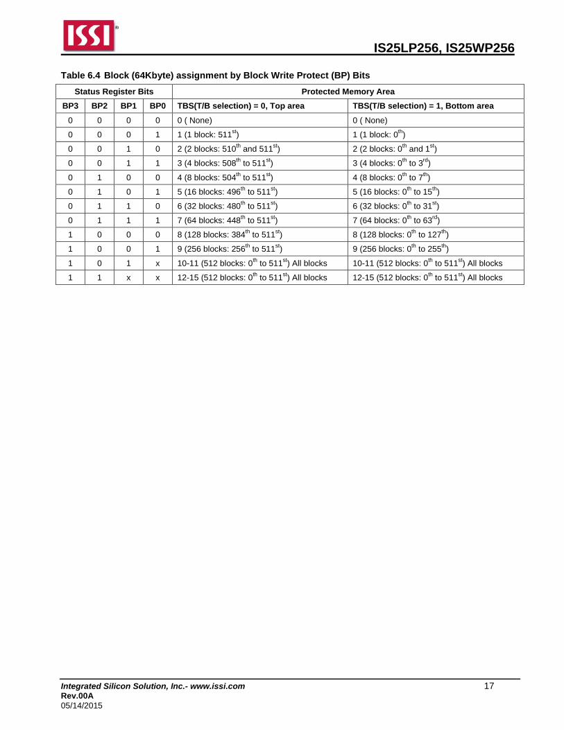
Table 6.4 Block (64Kbyte) assignment by Block Write Protect (BP) Bits
Status Register Bits Protected Memory Area
BP3 BP2 BP1 BP0 TBS(T/B selection) = 0, Top area TBS(T/B selection) = 1, Bottom area
0 0 0 0 0 ( None) 0 ( None)
0 0 0 1 1 (1 block: 511st) 1 (1 block: 0th)
0 0 1 0 2 (2 blocks: 510th and 511st) 2 (2 blocks: 0th and 1st)
0 0 1 1 3 (4 blocks: 508th to 511st) 3 (4 blocks: 0th to 3rd)
0 1 0 0 4 (8 blocks: 504th to 511st) 4 (8 blocks: 0th to 7th)
0 1 0 1 5 (16 blocks: 496th to 511st) 5 (16 blocks: 0th to 15th)
0 1 1 0 6 (32 blocks: 480th to 511st) 6 (32 blocks: 0th to 31st)
0 1 1 1 7 (64 blocks: 448th to 511st) 7 (64 blocks: 0th to 63rd)
1 0 0 0 8 (128 blocks: 384th to 511st) 8 (128 blocks: 0th to 127th)
1 0 0 1 9 (256 blocks: 256th to 511st) 9 (256 blocks: 0th to 255th)
1 0 1 x 10-11 (512 blocks: 0th to 511st) All blocks 10-11 (512 blocks: 0th to 511st) All blocks
1 1 x x 12-15 (512 blocks: 0th to 511st) All blocks 12-15 (512 blocks: 0th to 511st) All blocks
IS25LP256, IS25WP256
Integrated Silicon Solution, Inc.- www.issi.com 18 Rev.00A 05/14/2015
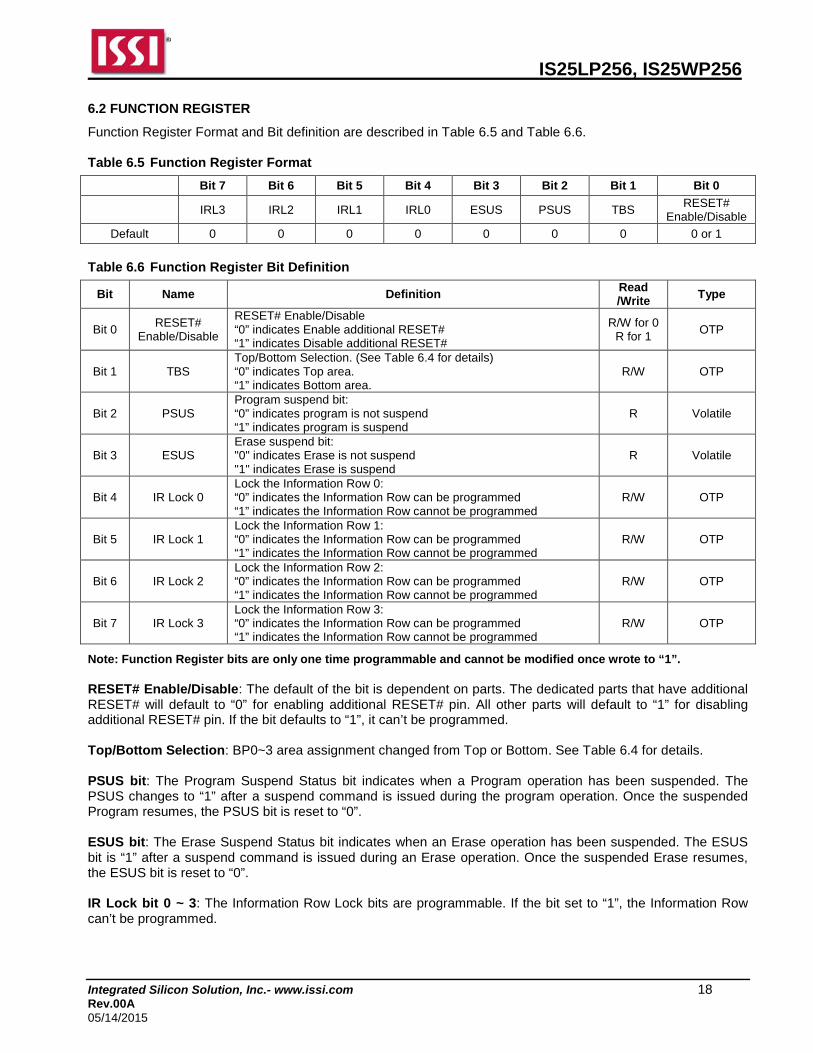
6.2 FUNCTION REGISTER
Function Register Format and Bit definition are described in Table 6.5 and Table 6.6. Table 6.5 Function Register Format
Bit 7 Bit 6 Bit 5 Bit 4 Bit 3 Bit 2 Bit 1 Bit 0
IRL3 IRL2 IRL1 IRL0 ESUS PSUS TBS RESET# Enable/Disable
Default 0 0 0 0 0 0 0 0 or 1
Table 6.6 Function Register Bit Definition
Bit Name Definition Read /Write Type
Bit 0 RESET# Enable/Disable
RESET# Enable/Disable “0” indicates Enable additional RESET# “1” indicates Disable additional RESET#
R/W for 0 R for 1 OTP
Bit 1 TBS Top/Bottom Selection. (See Table 6.4 for details) “0” indicates Top area. “1” indicates Bottom area.
R/W OTP
Bit 2 PSUS Program suspend bit: “0” indicates program is not suspend “1” indicates program is suspend
R Volatile
Bit 3 ESUS Erase suspend bit: "0" indicates Erase is not suspend "1" indicates Erase is suspend
R Volatile
Bit 4
IR Lock 0
Lock the Information Row 0: “0” indicates the Information Row can be programmed “1” indicates the Information Row cannot be programmed
R/W OTP
Bit 5 IR Lock 1 Lock the Information Row 1: “0” indicates the Information Row can be programmed “1” indicates the Information Row cannot be programmed
R/W OTP
Bit 6 IR Lock 2 Lock the Information Row 2: “0” indicates the Information Row can be programmed “1” indicates the Information Row cannot be programmed
R/W OTP
Bit 7 IR Lock 3 Lock the Information Row 3: “0” indicates the Information Row can be programmed “1” indicates the Information Row cannot be programmed
R/W OTP
Note: Function Register bits are only one time programmable and cannot be modified once wrote to “1”. RESET# Enable/Disable: The default of the bit is dependent on parts. The dedicated parts that have additional RESET# will default to “0” for enabling additional RESET# pin. All other parts will default to “1” for disabling additional RESET# pin. If the bit defaults to “1”, it can’t be programmed. Top/Bottom Selection: BP0~3 area assignment changed from Top or Bottom. See Table 6.4 for details. PSUS bit: The Program Suspend Status bit indicates when a Program operation has been suspended. The PSUS changes to “1” after a suspend command is issued during the program operation. Once the suspended Program resumes, the PSUS bit is reset to “0”. ESUS bit: The Erase Suspend Status bit indicates when an Erase operation has been suspended. The ESUS bit is “1” after a suspend command is issued during an Erase operation. Once the suspended Erase resumes, the ESUS bit is reset to “0”. IR Lock bit 0 ~ 3: The Information Row Lock bits are programmable. If the bit set to “1”, the Information Row can’t be programmed.
IS25LP256, IS25WP256
Integrated Silicon Solution, Inc.- www.issi.com 19 Rev.00A 05/14/2015
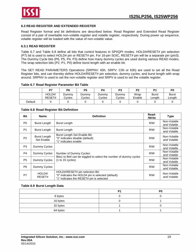
6.3 READ REGISTER AND EXTENDED REGISTER
Read Register format and bit definitions are described below. Read Register and Extended Read Register consist of a pair of rewritable non-volatile register and volatile register, respectively. During power up sequence, volatile register will be loaded with the value of non-volatile value. 6.3.1 READ REGISTER
Table 6.7 and Table 6.8 define all bits that control features in SPI/QPI modes. HOLD#/RESET# pin selection (P7) bit is used to select HOLD# pin or RESET# pin. For 16-pin SOIC, RESET# pin will be a separate pin (pin3). The Dummy Cycle bits (P6, P5, P4, P3) define how many dummy cycles are used during various READ modes. The wrap selection bits (P2, P1, P0) define burst length with an enable bit. The SET READ PARAMETERS Operations (SRPNV: 65h, SRPV: C0h or 63h) are used to set all the Read Register bits, and can thereby define HOLD#/RESET# pin selection, dummy cycles, and burst length with wrap around. SRPNV is used to set the non-volatile register and SRPV is used to set the volatile register. Table 6.7 Read Register Parameter Bit Table
P7 P6 P5 P4 P3 P2 P1 P0
HOLD#/ RESET#
Dummy Cycles
Dummy Cycles
Dummy Cycles
Dummy Cycles
Wrap Enable
Burst Length
Burst Length
Default 0 0 0 0 0 0 0 0
Table 6.8 Read Register Bit Definition
Bit Name Definition Read- /Write Type
P0 Burst Length Burst Length R/W Non-Volatile and Volatile
P1 Burst Length Burst Length R/W Non-Volatile and Volatile
P2 Burst Length Set Enable
Burst Length Set Enable Bit: "0" indicates disable (default) "1" indicates enable
R/W Non-Volatile and Volatile
P3 Dummy Cycles
Number of Dummy Cycles: Bits1 to Bit4 can be toggled to select the number of dummy cycles (1 to 15 cycles)
R/W Non-Volatile and Volatile
P4 Dummy Cycles R/W Non-Volatile and Volatile
P5 Dummy Cycles R/W Non-Volatile and Volatile
P6 Dummy Cycles R/W Non-Volatile and Volatile
P7 HOLD#/ RESET#
HOLD#/RESET# pin selection Bit: "0" indicates the HOLD# pin is selected (default) "1" indicates the RESET# pin is selected
R/W Non-Volatile and Volatile
Table 6.9 Burst Length Data
P1 P0
8 bytes 0 0
16 bytes 0 1
32 bytes 1 0
64 bytes 1 1
IS25LP256, IS25WP256
Integrated Silicon Solution, Inc.- www.issi.com 20 Rev.00A 05/14/2015
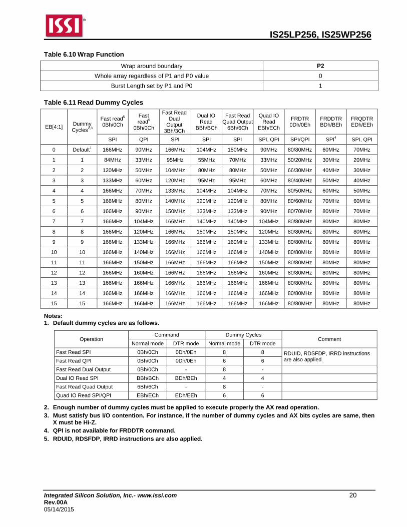
Table 6.10 Wrap Function
Wrap around boundary P2
Whole array regardless of P1 and P0 value 0
Burst Length set by P1 and P0 1
Table 6.11 Read Dummy Cycles
EB[4:1] Dummy Cycles2,3
Fast read5 0Bh/0Ch
Fast read5
0Bh/0Ch
Fast Read Dual
Output 3Bh/3Ch
Dual IO Read
BBh/BCh
Fast Read Quad Output
6Bh/6Ch
Quad IO Read
EBh/ECh
FRDTR 0Dh/0Eh
FRDDTR BDh/BEh
FRQDTR EDh/EEh
SPI QPI SPI SPI SPI SPI, QPI SPI/QPI SPI4 SPI, QPI
0 Default1 166MHz 90MHz 166MHz 104MHz 150MHz 90MHz 80/80MHz 60MHz 70MHz
1 1 84MHz 33MHz 95MHz 55MHz 70MHz 33MHz 50/20MHz 30MHz 20MHz
2 2 120MHz 50MHz 104MHz 80MHz 80MHz 50MHz 66/30MHz 40MHz 30MHz
3 3 133MHz 60MHz 120MHz 95MHz 95MHz 60MHz 80/40MHz 50MHz 40MHz
4 4 166MHz 70MHz 133MHz 104MHz 104MHz 70MHz 80/50MHz 60MHz 50MHz
5 5 166MHz 80MHz 140MHz 120MHz 120MHz 80MHz 80/60MHz 70MHz 60MHz
6 6 166MHz 90MHz 150MHz 133MHz 133MHz 90MHz 80/70MHz 80MHz 70MHz
7 7 166MHz 104MHz 166MHz 140MHz 140MHz 104MHz 80/80MHz 80MHz 80MHz
8 8 166MHz 120MHz 166MHz 150MHz 150MHz 120MHz 80/80MHz 80MHz 80MHz
9 9 166MHz 133MHz 166MHz 166MHz 160MHz 133MHz 80/80MHz 80MHz 80MHz
10 10 166MHz 140MHz 166MHz 166MHz 166MHz 140MHz 80/80MHz 80MHz 80MHz
11 11 166MHz 150MHz 166MHz 166MHz 166MHz 150MHz 80/80MHz 80MHz 80MHz
12 12 166MHz 160MHz 166MHz 166MHz 166MHz 160MHz 80/80MHz 80MHz 80MHz
13 13 166MHz 166MHz 166MHz 166MHz 166MHz 166MHz 80/80MHz 80MHz 80MHz
14 14 166MHz 166MHz 166MHz 166MHz 166MHz 166MHz 80/80MHz 80MHz 80MHz
15 15 166MHz 166MHz 166MHz 166MHz 166MHz 166MHz 80/80MHz 80MHz 80MHz
Notes: 1. Default dummy cycles are as follows.
Operation Command Dummy Cycles
Comment Normal mode DTR mode Normal mode DTR mode
Fast Read SPI 0Bh/0Ch 0Dh/0Eh 8 8 RDUID, RDSFDP, IRRD instructions are also applied. Fast Read QPI 0Bh/0Ch 0Dh/0Eh 6 6
Fast Read Dual Output 0Bh/0Ch - 8 -
Dual IO Read SPI BBh/BCh BDh/BEh 4 4
Fast Read Quad Output 6Bh/6Ch - 8 -
Quad IO Read SPI/QPI EBh/ECh EDh/EEh 6 6
2. Enough number of dummy cycles must be applied to execute properly the AX read operation. 3. Must satisfy bus I/O contention. For instance, if the number of dummy cycles and AX bits cycles are same, then
X must be Hi-Z. 4. QPI is not available for FRDDTR command. 5. RDUID, RDSFDP, IRRD instructions are also applied.
IS25LP256, IS25WP256
Integrated Silicon Solution, Inc.- www.issi.com 21 Rev.00A 05/14/2015
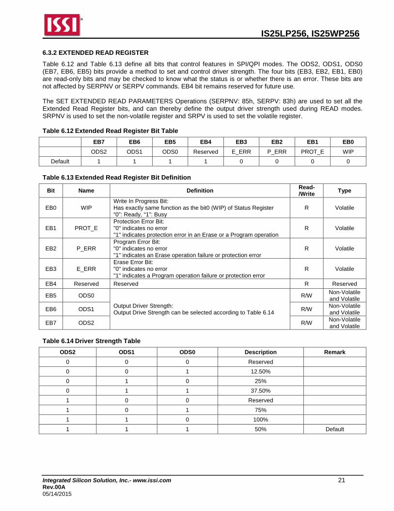
6.3.2 EXTENDED READ REGISTER
Table 6.12 and Table 6.13 define all bits that control features in SPI/QPI modes. The ODS2, ODS1, ODS0 (EB7, EB6, EB5) bits provide a method to set and control driver strength. The four bits (EB3, EB2, EB1, EB0) are read-only bits and may be checked to know what the status is or whether there is an error. These bits are not affected by SERPNV or SERPV commands. EB4 bit remains reserved for future use. The SET EXTENDED READ PARAMETERS Operations (SERPNV: 85h, SERPV: 83h) are used to set all the Extended Read Register bits, and can thereby define the output driver strength used during READ modes. SRPNV is used to set the non-volatile register and SRPV is used to set the volatile register. Table 6.12 Extended Read Register Bit Table
EB7 EB6 EB5 EB4 EB3 EB2 EB1 EB0
ODS2 ODS1 ODS0 Reserved E_ERR P_ERR PROT_E WIP
Default 1 1 1 1 0 0 0 0
Table 6.13 Extended Read Register Bit Definition
Bit Name Definition Read- /Write Type
EB0 WIP Write In Progress Bit: Has exactly same function as the bit0 (WIP) of Status Register “0”: Ready, “1”: Busy
R Volatile
EB1 PROT_E Protection Error Bit: "0" indicates no error "1" indicates protection error in an Erase or a Program operation
R Volatile
EB2 P_ERR Program Error Bit: "0" indicates no error "1" indicates an Erase operation failure or protection error
R Volatile
EB3 E_ERR Erase Error Bit: "0" indicates no error "1" indicates a Program operation failure or protection error
R Volatile
EB4 Reserved Reserved R Reserved
EB5 ODS0
Output Driver Strength: Output Drive Strength can be selected according to Table 6.14
R/W Non-Volatile and Volatile
EB6 ODS1 R/W Non-Volatile and Volatile
EB7 ODS2 R/W Non-Volatile and Volatile
Table 6.14 Driver Strength Table
ODS2 ODS1 ODS0 Description Remark
0 0 0 Reserved 0 0 1 12.50% 0 1 0 25% 0 1 1 37.50% 1 0 0 Reserved 1 0 1 75% 1 1 0 100% 1 1 1 50% Default
IS25LP256, IS25WP256
Integrated Silicon Solution, Inc.- www.issi.com 22 Rev.00A 05/14/2015
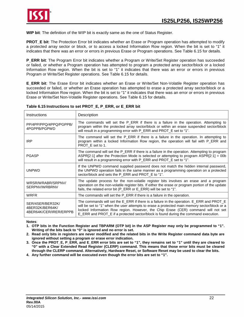
WIP bit: The definition of the WIP bit is exactly same as the one of Status Register. PROT_E bit: The Protection Error bit indicates whether an Erase or Program operation has attempted to modify a protected array sector or block, or to access a locked Information Row region. When the bit is set to “1” it indicates that there was an error or errors in previous Erase or Program operations. See Table 6.15 for details. P_ERR bit: The Program Error bit indicates whether a Program or Write/Set Register operation has succeeded or failed, or whether a Program operation has attempted to program a protected array sector/block or a locked Information Row region. When the bit is set to “1” it indicates that there was an error or errors in previous Program or Write/Set Register operations. See Table 6.15 for details. E_ERR bit: The Erase Error bit indicates whether an Erase or Write/Set Non-Volatile Register operation has succeeded or failed, or whether an Erase operation has attempted to erase a protected array sector/block or a locked Information Row region. When the bit is set to “1” it indicates that there was an error or errors in previous Erase or Write/Set Non-Volatile Register operations. See Table 6.15 for details. Table 6.15 Instructions to set PROT_E, P_ERR, or E_ERR bit
Instructions Description
PP/4PP/PPQ/4PPQ/PGPPB/ 4PGPPB/PGPWD
The commands will set the P_ERR if there is a failure in the operation. Attempting to program within the protected array sector/block or within an erase suspended sector/block will result in a programming error with P_ERR and PROT_E set to “1”.
IRP The command will set the P_ERR if there is a failure in the operation. In attempting to program within a locked Information Row region, the operation will fail with P_ERR and PROT_E set to 1.
PGASP The command will set the P_ERR if there is a failure in the operation. Attempting to program ASPR[2:1] after the Protection Mode is selected or attempting to program ASPR[2:1] = 00b will result in a programming error with P_ERR and PROT_E set to “1”.
UNPWD If the UNPWD command supplied password does not match the hidden internal password, the UNPWD operation fails in the same manner as a programming operation on a protected sector/block and sets the P_ERR and PROT_E to “1”.
WRSR/WRABR/SRPNV/ SERPNV/WRBRNV
The update process for the non-volatile register bits involves an erase and a program operation on the non-volatile register bits. If either the erase or program portion of the update fails, the related error bit (P_ERR or E_ERR) will be set to “1”.
WRFR The commands will set the P_ERR if there is a failure in the operation.
SER/4SER/BER32K/ 4BER32K/BER64K/ 4BER64K/CER/IRER/ERPPB
The commands will set the E_ERR if there is a failure in the operation. E_ERR and PROT_E will be set to “1” when the user attempts to erase a protected main memory sector/block or a locked Information Row region. However, the Chip Erase (CER) command will not set E_ERR and PROT_E if a protected sector/block is found during the command execution.
Notes: 1. OTP bits in the Function Register and TBPARM (OTP bit) in the ASP Register may only be programmed to “1”.
Writing of the bits back to “0” is ignored and no error is set. 2. Read only bits in registers are never modified and the related bits in the Write Register command data byte are
ignored without setting a program or erase error indication. 3. Once the PROT_E, P_ERR, and E_ERR error bits are set to “1”, they remains set to “1” until they are cleared to
“0” with a Clear Extended Read Register (CLERP) command. This means that those error bits must be cleared through the CLERP command. Alternatively, Hardware Reset, or Software Reset may be used to clear the bits.
4. Any further command will be executed even though the error bits are set to “1”.
IS25LP256, IS25WP256
Integrated Silicon Solution, Inc.- www.issi.com 23 Rev.00A 05/14/2015
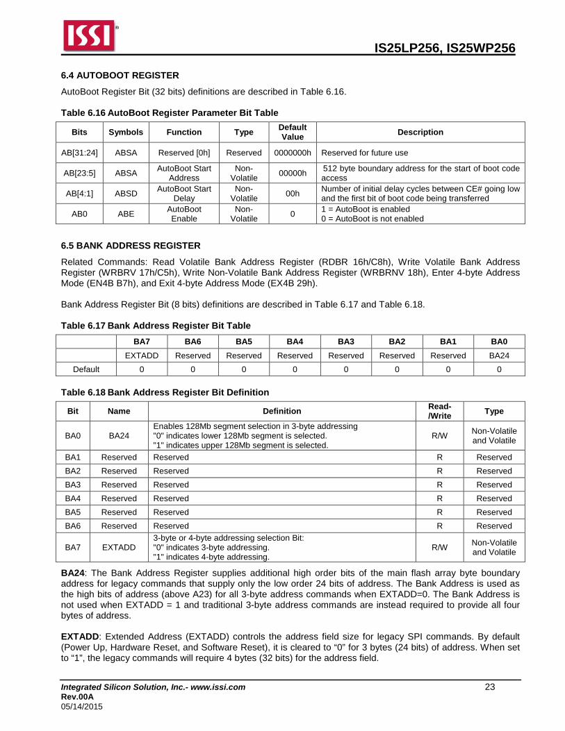
6.4 AUTOBOOT REGISTER
AutoBoot Register Bit (32 bits) definitions are described in Table 6.16. Table 6.16 AutoBoot Register Parameter Bit Table
Bits Symbols Function Type Default Value Description
AB[31:24] ABSA Reserved [0h] Reserved 0000000h Reserved for future use
AB[23:5] ABSA AutoBoot Start Address
Non-Volatile 00000h 512 byte boundary address for the start of boot code
access
AB[4:1] ABSD AutoBoot Start Delay
Non-Volatile 00h Number of initial delay cycles between CE# going low
and the first bit of boot code being transferred
AB0 ABE AutoBoot Enable
Non-Volatile 0 1 = AutoBoot is enabled
0 = AutoBoot is not enabled
6.5 BANK ADDRESS REGISTER
Related Commands: Read Volatile Bank Address Register (RDBR 16h/C8h), Write Volatile Bank Address Register (WRBRV 17h/C5h), Write Non-Volatile Bank Address Register (WRBRNV 18h), Enter 4-byte Address Mode (EN4B B7h), and Exit 4-byte Address Mode (EX4B 29h). Bank Address Register Bit (8 bits) definitions are described in Table 6.17 and Table 6.18. Table 6.17 Bank Address Register Bit Table
BA7 BA6 BA5 BA4 BA3 BA2 BA1 BA0
EXTADD Reserved Reserved Reserved Reserved Reserved Reserved BA24
Default 0 0 0 0 0 0 0 0
Table 6.18 Bank Address Register Bit Definition
Bit Name Definition Read- /Write Type
BA0 BA24 Enables 128Mb segment selection in 3-byte addressing "0" indicates lower 128Mb segment is selected. "1" indicates upper 128Mb segment is selected.
R/W Non-Volatile and Volatile
BA1 Reserved Reserved R Reserved
BA2 Reserved Reserved R Reserved
BA3 Reserved Reserved R Reserved
BA4 Reserved Reserved R Reserved
BA5 Reserved Reserved R Reserved
BA6 Reserved Reserved R Reserved
BA7 EXTADD 3-byte or 4-byte addressing selection Bit: "0" indicates 3-byte addressing. "1" indicates 4-byte addressing.
R/W Non-Volatile and Volatile
BA24: The Bank Address Register supplies additional high order bits of the main flash array byte boundary address for legacy commands that supply only the low order 24 bits of address. The Bank Address is used as the high bits of address (above A23) for all 3-byte address commands when EXTADD=0. The Bank Address is not used when EXTADD = 1 and traditional 3-byte address commands are instead required to provide all four bytes of address. EXTADD: Extended Address (EXTADD) controls the address field size for legacy SPI commands. By default (Power Up, Hardware Reset, and Software Reset), it is cleared to “0” for 3 bytes (24 bits) of address. When set to “1”, the legacy commands will require 4 bytes (32 bits) for the address field.
IS25LP256, IS25WP256
Integrated Silicon Solution, Inc.- www.issi.com 24 Rev.00A 05/14/2015
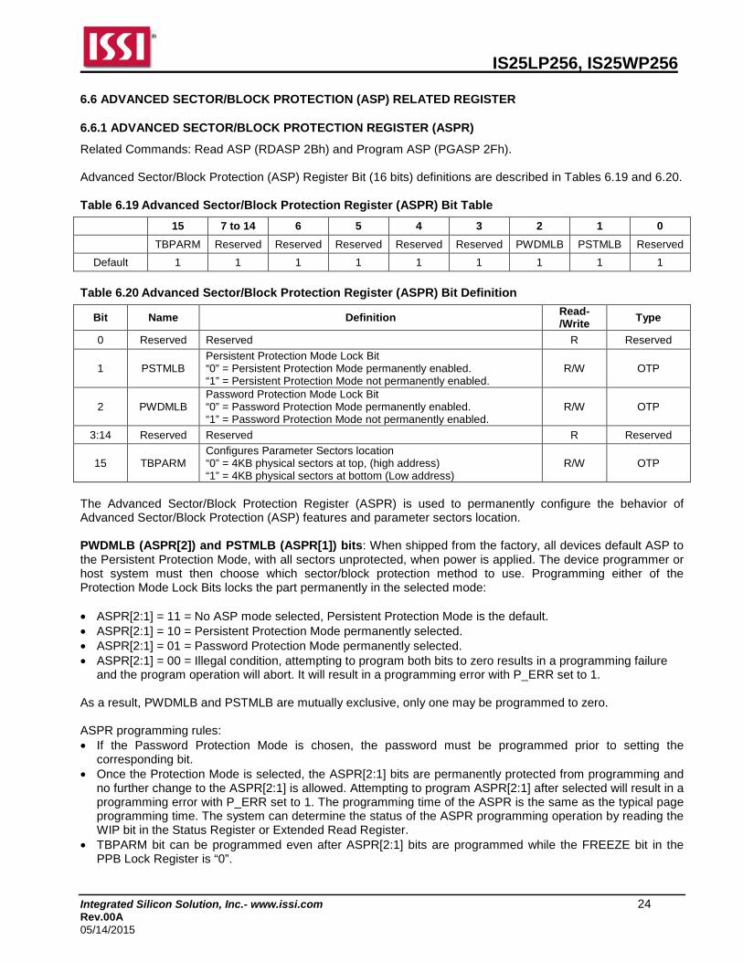
6.6 ADVANCED SECTOR/BLOCK PROTECTION (ASP) RELATED REGISTER
6.6.1 ADVANCED SECTOR/BLOCK PROTECTION REGISTER (ASPR)
Related Commands: Read ASP (RDASP 2Bh) and Program ASP (PGASP 2Fh). Advanced Sector/Block Protection (ASP) Register Bit (16 bits) definitions are described in Tables 6.19 and 6.20. Table 6.19 Advanced Sector/Block Protection Register (ASPR) Bit Table
15 7 to 14 6 5 4 3 2 1 0
TBPARM Reserved Reserved Reserved Reserved Reserved PWDMLB PSTMLB Reserved
Default 1 1 1 1 1 1 1 1 1
Table 6.20 Advanced Sector/Block Protection Register (ASPR) Bit Definition
Bit Name Definition Read- /Write Type
0 Reserved Reserved R Reserved
1 PSTMLB Persistent Protection Mode Lock Bit “0” = Persistent Protection Mode permanently enabled. “1” = Persistent Protection Mode not permanently enabled.
R/W OTP
2 PWDMLB Password Protection Mode Lock Bit “0” = Password Protection Mode permanently enabled. “1” = Password Protection Mode not permanently enabled.
R/W OTP
3:14 Reserved Reserved R Reserved
15 TBPARM Configures Parameter Sectors location “0” = 4KB physical sectors at top, (high address) “1” = 4KB physical sectors at bottom (Low address)
R/W OTP
The Advanced Sector/Block Protection Register (ASPR) is used to permanently configure the behavior of Advanced Sector/Block Protection (ASP) features and parameter sectors location. PWDMLB (ASPR[2]) and PSTMLB (ASPR[1]) bits: When shipped from the factory, all devices default ASP to the Persistent Protection Mode, with all sectors unprotected, when power is applied. The device programmer or host system must then choose which sector/block protection method to use. Programming either of the Protection Mode Lock Bits locks the part permanently in the selected mode: • ASPR[2:1] = 11 = No ASP mode selected, Persistent Protection Mode is the default. • ASPR[2:1] = 10 = Persistent Protection Mode permanently selected. • ASPR[2:1] = 01 = Password Protection Mode permanently selected. • ASPR[2:1] = 00 = Illegal condition, attempting to program both bits to zero results in a programming failure
and the program operation will abort. It will result in a programming error with P_ERR set to 1. As a result, PWDMLB and PSTMLB are mutually exclusive, only one may be programmed to zero. ASPR programming rules: • If the Password Protection Mode is chosen, the password must be programmed prior to setting the
corresponding bit. • Once the Protection Mode is selected, the ASPR[2:1] bits are permanently protected from programming and
no further change to the ASPR[2:1] is allowed. Attempting to program ASPR[2:1] after selected will result in a programming error with P_ERR set to 1. The programming time of the ASPR is the same as the typical page programming time. The system can determine the status of the ASPR programming operation by reading the WIP bit in the Status Register or Extended Read Register.
• TBPARM bit can be programmed even after ASPR[2:1] bits are programmed while the FREEZE bit in the PPB Lock Register is “0”.

IS25LP256, IS25WP256
Integrated Silicon Solution, Inc.- www.issi.com 25 Rev.00A 05/14/2015
TBPARM bit: TBPARM defines the logical location of the parameter block. The parameter block consists of thirty-two 4KB sectors, which replace two 64KB blocks. When TBPARM is set to a “0” the parameter block is in the top of the memory array address space. When TBPARM is set to a “1” the parameter block is at the Bottom of the array. TBPARM is OTP and set to a “1” when it ships from Factory. If TBPARM is programmed to “0”, an attempt to change it back to “1” will fail and ignore the Program. The desired state of TBPARM must be selected during the initial configuration of the device during system manufacture; before the first program or erase operation on the main flash array. TBPARM must not be programmed after programming or erasing is done in the main flash array. TBS can be programmed independent of TBPARM. Therefore, the user can elect to store parameter information from the bottom of the array and protect boot code starting at the top of the array, and vice versa. Or the user can select to store and protect the parameter information starting from the top or bottom together. 6.6.2 PASSWORD REGISTER
Related Commands: Read Password (RDPWD E7h), Program Password (PGPWD E8h), and Unlock Password (UNPWD, E9h). Table 6.21 Password Register Bit Definition
Bit Name Definition Default Read- /Write Type
0:63 PSTMLB
64 bit hidden password: The password is no longer readable after the password protection mode is selected by programming ASPR bit 2 to zero.
FFFFFFFF- FFFFFFFFh R/W OTP
6.6.3 PPB LOCK REGISTER
Related Commands: Read PPB Lock Bit (RDPLB A7h), Write PPB Lock Bit (WRPLB A6h), and Set FREEZE Bit (SFRZ 91h). The WRPLB is available only in Persistent Protection Mode. Table 6.22 PPB Lock Register Bit Definition
Bit Name Definition Default Read- /Write Type
0 PPBLK
PPB Lock bit: Protect PPB Array “0” = PPB array protected until next power cycle
or Hardware Reset “1” = PPB array may be programmed or erased.
Persistent: 1 Password: 0 R/W Volatile
1:6 Reserved Reserved Reserved R Reserved
7 FREEZE
Lock current state of BP3-0 bits in Status Register, TBS in Function Register and TBPARM in ASPR, and Information Row (IR) regions. “1” = Locked “0” = Un-locked
0 R/W Volatile

IS25LP256, IS25WP256
Integrated Silicon Solution, Inc.- www.issi.com 26 Rev.00A 05/14/2015
PPBLK bit: The PPB Lock bit is a volatile bit for protecting all PPB bits. When cleared to 0, it locks all PPBs, when set to 1, it allows the PPBs to be changed. The WRPLB command is used to clear the PPB Lock bit to 0. The PPB Lock bit must be cleared to 0 only after all the PPBs are configured to the desired settings. In Persistent Protection mode, the PPB Lock bit is set to 1 during POR or Hardware Reset. When cleared to 0, no software command sequence can set the PPB Lock bit to 1, only another Hardware Reset or power-up can set the PPB Lock bit. In the Password Protection mode, the PPB Lock bit is cleared to 0 during POR or Hardware Reset. The PPB Lock bit can only be set to 1 by the Unlock Password command. FREEZE bit: FREEZE bit, when set to “1”, locks the current state of BP3-0 in Status Register, TBS in the Function Register, TBPARM in the Advanced Sector/Block Protection Register, and the Information Row. This prevents writing, programming, or erasing these areas. As long as FREEZE remains cleared to logic “0”, BP3-0 in Status Register, TBS in the Function Register, and TBPARM in the Advanced Sector/Block Protection Register are writable and the Information Row is programmable. Once FREEZE has been written to a logic “1” it can only be cleared to a logic “0” by a power-on cycle or a Hardware Reset. Software Reset will not affect the state of FREEZE. The FREEZE is volatile and the default state of FREEZE after power-on is “0”. The FREEZE can be set to “1” by a SFRZ command. 6.6.4 PPB REGISTER
Related Commands: Read PPB (RDPPB FCh or 4RDPPB E2h)), Program PPB (PGPPB FDh or 4PGPPB E3h), and Erase PPB (ERPPB E4h). Table 6.23 PPB Register Bit Definition
Bit Name Definition Default Read- /Write Type
0:7 PPB
Read or Program per sector/block PPB: 00h = PPB for the sector/block addressed by the PPBRD or
PPBP command is programmed to “0”, protecting that sector/block from program or erase operations.
FFh = PPB for the sector/block addressed by the PPBRD or PPBP command is erased to “1”, not protecting that sector/block from program or erase operations.
FFh R/W Non-Volatile
6.6.5 DYB REGISTER
Related Commands: Read DYB (RDDYB FAh or 4RDDYB E0h) and Write DYB (WRDYB FBh or 4WRDYB E1h). Table 6.24 DYB Register Bit Definition
Bit Name Definition Default Read- /Write Type
0:7 DYB
Read or Write per sector/block DYB: 00h = DYB for the sector/block addressed by the DYBRD or
DYBP command is cleared to “0”, protecting that sector/block from program or erase operations.
FFh = DYB for the sector/block addressed by the DYBRD or DYBP command is set to “1”, not protecting that sector/block from program or erase operations.
FFh R/W Volatile
IS25LP256, IS25WP256
Integrated Silicon Solution, Inc.- www.issi.com 27 Rev.00A 05/14/2015
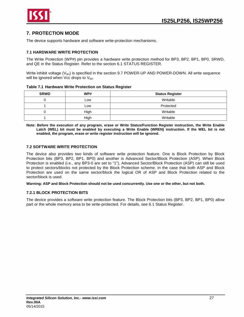
7. PROTECTION MODE
The device supports hardware and software write-protection mechanisms.
7.1 HARDWARE WRITE PROTECTION
The Write Protection (WP#) pin provides a hardware write protection method for BP3, BP2, BP1, BP0, SRWD, and QE in the Status Register. Refer to the section 6.1 STATUS REGISTER. Write inhibit voltage (VWI) is specified in the section 9.7 POWER-UP AND POWER-DOWN. All write sequence will be ignored when Vcc drops to VWI. Table 7.1 Hardware Write Protection on Status Register
SRWD WP# Status Register
0 Low Writable
1 Low Protected
0 High Writable
1 High Writable
Note: Before the execution of any program, erase or Write Status/Function Register instruction, the Write Enable Latch (WEL) bit must be enabled by executing a Write Enable (WREN) instruction. If the WEL bit is not enabled, the program, erase or write register instruction will be ignored.
7.2 SOFTWARE WRITE PROTECTION
The device also provides two kinds of software write protection feature. One is Block Protection by Block Protection bits (BP3, BP2, BP1, BP0) and another is Advanced Sector/Block Protection (ASP). When Block Protection is enabled (i.e., any BP3-0 are set to “1”), Advanced Sector/Block Protection (ASP) can still be used to protect sectors/blocks not protected by the Block Protection scheme. In the case that both ASP and Block Protection are used on the same sector/block the logical OR of ASP and Block Protection related to the sector/block is used.
Warning: ASP and Block Protection should not be used concurrently. Use one or the other, but not both. 7.2.1 BLOCK PROTECTION BITS
The device provides a software write protection feature. The Block Protection bits (BP3, BP2, BP1, BP0) allow part or the whole memory area to be write-protected. For details, see 6.1 Status Register.

IS25LP256, IS25WP256
Integrated Silicon Solution, Inc.- www.issi.com 28 Rev.00A 05/14/2015
7.2.2 ADVANCED SECTOR/BLOCK PROTECTION (ASP)
There are two ways to implement software Advanced Sector/Block Protection on this device: Password Protection method or Persistent Protection methods. Through these two protection methods, user can disable or enable the programming or erasing operation to any or all blocks including 32 top 4K sectors or 32 bottom 4K sectors. The Figure 7.1 shows an overview of these methods. Every main flash array block/top sector/bottom sector has a non-volatile (PPB) and a volatile (DYB) protection bit associated with it. When either bit is 0, the sector is protected from program and erase operations. The PPB bits are protected from program and erase when the PPB Lock bit is “0”. The PPB bits are erased so that all main flash array sectors are unprotected when shipped from factory. There are two methods for managing the state of the PPB Lock bit, Persistent Protection and Password Protection. The Persistent Protection Mode sets the PPB Lock bit to “1” during power up or Hardware Reset so that the PPB bits are unprotected. There is a WRPLB command to clear the PPB Lock bit to “0” to protect the PPB bits. There is no command in the Persistent Protection method to set the PPB Lock bit therefore the PPB Lock bit will remain at “0” until the next power up or Hardware Reset. The Persistent Protection method allows boot code the option of changing sector protection by programming or erasing the PPB, then protecting the PPB from further change for the remainder of normal system operation by clearing the PPB Lock bit. This is sometimes called Boot-code controlled sector protection. The Password Protection Mode requires use of a password to control PPB protection. In the Password Protection Mode, the PPB Lock bit is cleared to “0” during power up or Hardware Reset to protect the PPB bits. A 64-bit password may be permanently programmed and hidden for the Password Protection Mode. The UNPWD command can be used to provide a password for comparison with the hidden password. If the password matches the PPB Lock bit is set to “1” to unprotect the PPB. The WRPLB command can be used to clear the PPB Lock bit to “0”. After clearing the PPB Lock bit to “0”, the UNPWD command can be used again to unprotect the PPB. The selection of the PPB Lock bit management method is made by programming OTP bits in the ASP Register so as to permanently select the method used.

IS25LP256, IS25WP256
Integrated Silicon Solution, Inc.- www.issi.com 29 Rev.00A 05/14/2015
1. 0 = PPBs Locked, 1 = PPBs Unlocked 2. The bit is volatile, and defaults to “1”
(Persistent Mode) or “0” (Password Mode) upon reset.
3. Programming to “0” locks all PPBs to their current state. 4. Password Method requires a
password to set PPB Lock bit to “1” to enable program or erase of PPB bits.
5. Persistent Method only allows PPB Lock bit to be cleared to ‘0’ to prevent program or erase of PPB bits. Power off or hardware reset required to set PPB Lock bit to “1”.
Persistent Protection Bit (PPB)
Memory Array
Sector/Block 0 DYB 0 PPB Lock Bit PPB 0
Sector/Block 1 DYB 1 PPB 1
Sector/Block 2 PPB 2
DYB 2
DYB 3 Sector/Block 3 PPB 3
Sector/Block N-3
Sector/Block
Sector/Block
DYB N-3
DYB N-2
DYB N-1
Sector/Block
DYB N
PPB N-3
PPB N
PPB N-2
PPB N-1
Figure 7.1 Advanced Sector/Block Protection
1. 0 = Sector/Block Protected 1 = Sector/Block Unprotected
2. The bit is volatile and defaults to “1” (Unprotected) after power up.
1. 0 = Sector/Block Protected
1 = Sector/Block Unprotected 2. PPBs programmed
individually, but erased collectively.
Note: N = 542 = 32 (32 Top 4K sectors or 32 Bottom 4K sectors) + 510 (510 64K blocks)
Dynamic Protection Bit (DYB)
Password Protection Mode (ASPR[2]=0)
ASP Register Bits (OTP)
Persistent Protection Mode (ASPR[1]=0)
64-bit Password (OTP)

IS25LP256, IS25WP256
Integrated Silicon Solution, Inc.- www.issi.com 30 Rev.00A 05/14/2015
Table 7.2 PPB/DYB and Sector/Block mapping (TPPARM = 0)
PPB Group DYB Group Block No. (64Kbyte) Sector No. Sector Size
(Kbyte) Address Range
PPB 0 DYB 0
Block 0
Sector 0 4 000000h - 000FFFh
: : : : :
: : : : :
PPB 15 DYB 15 Sector 15 4 00F000h - 00FFFFh
PPB 16 DYB 16
Block 1
Sector 16 4 010000h - 010FFFh
: : : : :
: : : : :
PPB 31 DYB 31 Sector 31 4 01F000h - 01FFFFh
PPB 32 DYB 32 Block 2
Sector 32 4 020000h - 020FFFh
: : :
: : :
Sector 47 4 02F000h - 02FFFFh
: : : : : :
PPB 284 DYB 284 Block 254
Sector 4064 4 FE0000h – FE0FFFh
: : :
: : :
Sector 4079 4 FEF000h – FEFFFFh
PPB 285 DYB 285 Block 255
Sector 4080 4 FF0000h – FF0FFFh
: : :
: : :
Sector 4095 4 FFF000h – FFFFFFh
: : : : : :
PPB 540 DYB 540 Block 510
Sector 8160 4 1FE0000h – 1FE0FFFh
: : :
: : :
Sector 8175 4 1FEF000h – 1FEFFFFh
PPB 541 DYB 541 Block 511
Sector 8176 4 1FF0000h – 1FF0FFFh
: : :
: : :
Sector 8191 4 1FFF000h – 1FFFFFFh

IS25LP256, IS25WP256
Integrated Silicon Solution, Inc.- www.issi.com 31 Rev.00A 05/14/2015
Table 7.3 PPB/DYB and Sector/Block mapping (TPPARM = 1)
PPB Group DYB Group Block No. (64Kbyte) Sector No. Sector Size
(Kbyte) Address Range
PPB 0 DYB 0 Block 0
Sector 0 4 000000h - 000FFFh
: : :
: : :
Sector 15 4 00F000h - 00FFFFh
PPB 1 DYB 1 Block 1
Sector 16 4 010000h - 010FFFh
: : :
: : :
Sector 31 4 01F000h - 01FFFFh
PPB 2 DYB 2 Block 2
Sector 32 4 020000h - 020FFFh
: : :
: : :
Sector 47 4 02F000h - 02FFFFh
: : : : : :
PPB 254 DYB 254 Block 254
Sector 4064 4 FE0000h – FE0FFFh
: : :
: : :
Sector 4079 4 FEF000h – FEFFFFh
PPB 255 DYB 255 Block 255
Sector 4080 4 FF0000h – FF0FFFh
: : :
: : :
Sector 4095 4 FFF000h – FFFFFFh
: : : : : :
PPB 510 DYB 510
Block 510
Sector 8160 4 1FE0000h – 1FE0FFFh
: : : : :
: : : : :
PPB 525 DYB 525 Sector 8175 4 1FEF000h – 1FEFFFFh
PPB 525 DYB 526
Block 511
Sector 8176 4 1FF0000h – 1FF0FFFh
: : : : :
: : : : :
PPB 541 DYB 541 Sector 8191 4 1FFF000h – 1FFFFFFh
IS25LP256, IS25WP256
Integrated Silicon Solution, Inc.- www.issi.com 32 Rev.00A 05/14/2015
Persistent Protection Bits (PPBs)
The Persistent Protection Bits (PPBs) are unique for each sector/block and non-volatile (refer to Figure 7.1, Table 7.2, and Table 7.3). It is programmed individually but must be erased as a group, similar to the way individual words may be programmed in the main array but an entire sector/block must be erased at the same time. The PPBs have the same endurances as the Flash memory. Preprogramming and verification prior to erasure are handled by the device, and therefore do not require system monitoring. Programming a PPB bit requires the typical page programming time. Erasing all the PPBs requires typical sector erase time. During PPB bit programming and PPB bit erasing, status is available by reading the Status Register or Extended Read Register. Reading of a PPB bit requires the initial access time of the device. Notes: 1. Each PPB is individually programmed to “0” and all are erased to “1” in parallel. 2. The PPB Lock bit must be cleared first before changing the status of a PPB. 3. While programming PPB, array data cannot be read from any sectors/blocks. 4. When reading the PPB of the desired sector/block the address should be location zero within the sector/block. The high
order address bits not used must be zero. 5. There are no means for individually erasing a specific PPB and no specific sector/block address is required for this
operation. 6. The state of the PPB for a given sector/block can be verified by using a PPB Read command. 7. When the parts are first shipped, the PPBs are cleared (erased to “1”). Dynamic Protection Bits (DYBs)
Dynamic Protection Bits (DYBs) are volatile and unique for each sector/block and can be individually modified. DYBs only control the protection for unprotected sectors/blocks that have their PPBs cleared (erased to “1”). By issuing the Write DYB command, the DYBs are cleared to “0” or set to “1”, thus placing each sector/block in the protected or unprotected state respectively. This feature allows software to easily protect sectors/blocks against inadvertent changes, yet does not prevent the easy removal of protection when changes are needed. The DYBs can be set or cleared as often as needed as they are volatile bits. Persistent Protection Bit (PPB) Lock Bit
The PPB Lock bit is a volatile bit for protecting all PPB bits. When cleared to “0”, it locks all PPBs and when set to “1”, it allows the PPBs to be changed. . If the PPB Lock bit is “0”, the PPB Program or Erase command does not execute and fails without programming or erasing the PPB. In Persistent Protection mode, the PPB Lock bit is set to “1” during power up or Hardware Reset. When cleared to “0”, no software command sequence can set the PPB Lock bit to “1”, only another Hardware Reset or power-up can set the PPB Lock bit. In the Password Protection mode, the PPB Lock bit is cleared to “0” during power up or a Hardware Reset during power up or a Hardware Reset during power up or a Hardware Reset. The PPB Lock bit can only be set to “1” by the Password Unlock command. The PPB Lock bit must be cleared to “0” only after all PPBs are configured to the desired settings.
IS25LP256, IS25WP256
Integrated Silicon Solution, Inc.- www.issi.com 33 Rev.00A 05/14/2015
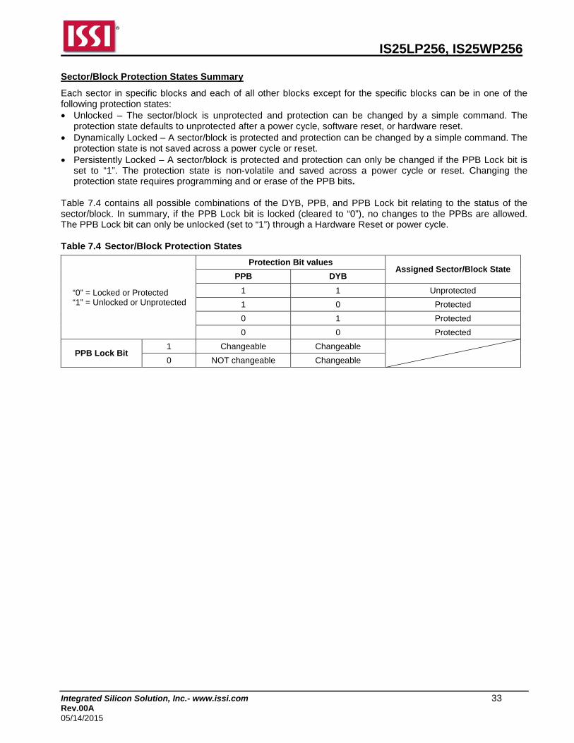
Sector/Block Protection States Summary
Each sector in specific blocks and each of all other blocks except for the specific blocks can be in one of the following protection states: • Unlocked – The sector/block is unprotected and protection can be changed by a simple command. The
protection state defaults to unprotected after a power cycle, software reset, or hardware reset. • Dynamically Locked – A sector/block is protected and protection can be changed by a simple command. The
protection state is not saved across a power cycle or reset. • Persistently Locked – A sector/block is protected and protection can only be changed if the PPB Lock bit is
set to “1”. The protection state is non-volatile and saved across a power cycle or reset. Changing the protection state requires programming and or erase of the PPB bits.
Table 7.4 contains all possible combinations of the DYB, PPB, and PPB Lock bit relating to the status of the sector/block. In summary, if the PPB Lock bit is locked (cleared to “0”), no changes to the PPBs are allowed. The PPB Lock bit can only be unlocked (set to “1”) through a Hardware Reset or power cycle. Table 7.4 Sector/Block Protection States
“0” = Locked or Protected “1” = Unlocked or Unprotected
Protection Bit values Assigned Sector/Block State
PPB DYB
1 1 Unprotected
1 0 Protected
0 1 Protected
0 0 Protected
PPB Lock Bit 1 Changeable Changeable
0 NOT changeable Changeable

IS25LP256, IS25WP256
Integrated Silicon Solution, Inc.- www.issi.com 34 Rev.00A 05/14/2015
Persistent Protection Mode
The Persistent Protection Mode sets the PPB Lock bit to “1” during power up or Hardware Reset so that the PPB bits are unprotected by a device Hardware Reset. Software Reset does not affect the PPB Lock bit. The WRPLB command can clear the PPB Lock bit to “0” to protect the PPB. There is no command to set the PPB Lock bit therefore the PPB Lock bit will remain at “0” until the next power up or Hardware Reset. Password Protection Mode
The Password Protection Mode allows an even higher level of security than the Persistent Protection Mode by requiring a 64-bit password for unlocking the device PPB Lock bit. In addition to this password requirement, after power up or Hardware Reset, the PPB Lock bit is cleared to “0” to maintain the password mode of operation. Successful execution of the Unlock Password command by entering the entire password sets the PPB Lock bit to “1”, allowing for sector/block PPBs modifications. Notes: 1. The password is all “1”s when shipped from Factory. It is located in its own memory space and is accessible through the
use of the Program Password and Read Password commands. 2. Once the Password is programmed and verified, the Password Protection Mode Lock Bit (ASPR[2]=0) in ASP Register
must be programmed in order to prevent reading or modifying the password. After the Password Protection Mode Lock Bit is programmed, all further Program and Read commands to the password region are disabled and these commands are ignored so that there is no means to verify what the password is. Password verification is only allowed before selecting the Password Protection Mode.
3. The Program Password Command is only capable of programming “0”s. Programming a “1” after a cell is programmed as a “0” results in the cell left as a “0” with no programming error.
4. All 64-bit password combinations are valid as a password. 5. The Protection Mode Lock Bits in ASP Register are not erasable because they are OTP. 6. The exact password must be entered in order for the unlocking function to occur. If the password provided by Unlock
Password command does not match the hidden internal password, the unlock operation fails in the same manner as a programming operation on a protected sector/block. The P_ERR and PROT_E are set to 1 and the PPB Lock bit remains cleared to 0. In this case it is a failure to change the state of the PPB Lock bit because it is still protected by the lack of a valid password.
7. The Unlock Password command cannot be accepted any faster than once every 100µs ± 20µs. This makes it take an unreasonably long time (58 million years) for a hacker to run through all the 64-bit combinations in an attempt to correctly match a password. The Read Status Register command or the Read Extended Read Register may be used to read the WIP bit to determine when the device has completed the Unlock Password command or is ready to accept a new password command. When a valid password is provided the Unlock Password command does not insert the 100µs delay before returning the WIP bit to zero.
8. If the password is lost after selecting the Password Protection Mode, there is no way to set the PPB Lock bit.

IS25LP256, IS25WP256
Integrated Silicon Solution, Inc.- www.issi.com 35 Rev.00A 05/14/2015
8. DEVICE OPERATION
8.1 COMMAND OVERVIEW
The device utilizes an 8-bit instruction register. Refer to Table 8.4. Instruction Set for details on instructions and instruction codes. All instructions, addresses, and data are shifted in with the most significant bit (MSB) first on Serial Data Input (SI) or Serial Data IOs (IO0, IO1, IO2, IO3). The input data on SI or IOs is latched on the rising edge of Serial Clock (SCK) for normal mode and both of rising and falling edges for DTR mode after Chip Enable (CE#) is driven low (VIL). Every instruction sequence starts with a one-byte instruction code and is followed by address bytes and/or dummy cycles (configurable) and/or data bytes, depending on the type of instruction. CE# must be driven high (VIH) after the last bit of the instruction sequence has been shifted in to end the operation. Commands are structured as follows: • Each command begins with a byte (eight bits) instruction. • The instruction may be stand alone or may be followed by address bits to select a location within one of
several address spaces in the device. The address may be either a 24-bit or 32-bit byte boundary address. • The SPI interface with Multiple IO provides the option for each transfer of address and data information to be
done one, two, or four bits in parallel. This enables a tradeoff between the number of signal connections (IO bus width) and the speed of information transfer. If the host system can support a two or four bit wide IO bus the memory performance can be increased by using the instructions that provide parallel two bit (dual) or parallel four bit (quad) transfers.
• The width of all transfers following the instruction are determined by the instruction sent. • All single bit or parallel bit groups are transferred in most to least significant bit order. • Some instructions send Mode Bits following the address to indicate that the next command will be of the
same type with an implied, rather than an explicit, instruction. The next command thus does not provide an instruction byte, only a new address and mode bits. This reduces the time needed to send each command when the same command type is repeated in a sequence of commands.
• The address or Mode Bits may be followed by Dummy Cycles before read data is returned to the host. • Dummy Cycles may be zero to several SCK cycles. In fact, Mode Bits will be counted as a part of Dummy
Cycles. • All instruction, address, Mode, and data information is transferred in byte granularity. Addresses are shifted
into the device with the Most Significant Byte first. All data is transferred with the lowest address byte sent first. Following bytes of data are sent in lowest to highest byte address order i.e. the byte address increments.
• All attempts to read the flash memory array during a program, erase, or a write cycle (embedded operations) are ignored. The embedded operation will continue to execute without any affect. A very limited set of commands are accepted during an embedded operation. These are discussed in the individual command descriptions. While a program, erase, or write operation is in progress, it is recommended to check that the Write In Progress (WIP) bit is “0” before issuing most commands to the device, to ensure the new command can be accepted.
• Depending on the command, the time for execution varies. A command to read status information from an executing command is available to determine when the command completes execution and whether the command was successful.
• Following are some general signal relationship descriptions to keep in mind. – The host always controls the Chip Enable (CE#), Serial Clock (SCK), and Serial Input (SI) - SI for single
bit wide transfers. The memory drives Serial Output (SO) for single bit read transfers. The host and memory alternately drive the IO0-IO3 signals during Dual and Quad transfers.
– All commands begin with the host selecting the memory by driving CE# low before the first rising edge of SCK. CE# is kept low throughout a command and when CE# is returned high the command ends.
Generally, CE# remains low for 8-bit transfer multiples to transfer byte granularity information. All commands will not be accepted if CE# is returned high not at an 8-bit boundary.

IS25LP256, IS25WP256
Integrated Silicon Solution, Inc.- www.issi.com 36 Rev.00A 05/14/2015
8.2 COMMAND SET SUMMARY
Extended Addressing
To accommodate addressing above 128Mb (24-bit), there are three options: 1. New instructions with 4-byte (32-bit) address. See Table 8.2.
2. 4-byte addressing with the 3-byte address instructions: For backward compatibility to the 3-byte address instructions, the standard instructions can be used in conjunction with the EXTADD Bit in the Bank Address Register (BAR[7]) or Enter 4-byte Address Mode to switch from 3 bytes to 4 bytes of address field. When EXTADD bit is set to 1 or Enter 4-byte Address Mode command is issued only in the case that EXTADD bit = 0, the instructions are changed to require 4-byte (32-bit) for the address field. See Table 8.3.
3. 3-byte addressing with the 3-byte address instructions: For backward compatibility to the 3-byte addressing, the standard instructions can be used in conjunction with the Bank Address Register. See Table 8.3. • The Bank Address Register is used to switch between 128Mbit (16Mbyte) banks of memory, the standard
3-byte address selects an address within the bank selected by the Bank Address Register. o The host system writes the Bank Address Register to access beyond the first 128Mbit of memory. o This applies to read, erase, and program commands.
• The Bank Address Register provides the high order (4th) byte of address, which is used to address the available memory at addresses greater than 128Mbit.
• Bank Address Register bits are volatile. o On power up, the default is Bank0 (the lowest address 16 Mbytes).
• For Read, the device will continuously transfer out data until the end of the array. o There is no bank to bank delay. o The Bank Address Register is not updated. o The Bank Address Register value is used only for the initial address of an access.
Table 8.1 Bank Address Map
Bank Address Register Bit 0 Bank Memory Array Address Range
0 0 00000000h 00FFFFFFh
1 1 01000000h 01FFFFFFh
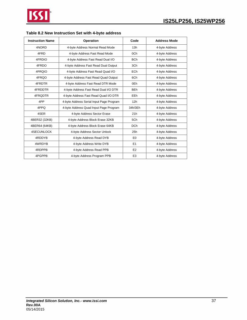
IS25LP256, IS25WP256
Integrated Silicon Solution, Inc.- www.issi.com 37 Rev.00A 05/14/2015
Table 8.2 New Instruction Set with 4-byte address
Instruction Name Operation Code Address Mode
4NORD 4-byte Address Normal Read Mode 13h 4-byte Address
4FRD 4-byte Address Fast Read Mode 0Ch 4-byte Address
4FRDIO 4-byte Address Fast Read Dual I/O BCh 4-byte Address
4FRDO 4-byte Address Fast Read Dual Output 3Ch 4-byte Address
4FRQIO 4-byte Address Fast Read Quad I/O ECh 4-byte Address
4FRQO 4-byte Address Fast Read Quad Output 6Ch 4-byte Address
4FRDTR 4-byte Address Fast Read DTR Mode 0Eh 4-byte Address
4FRDDTR 4-byte Address Fast Read Dual I/O DTR BEh 4-byte Address
4FRQDTR 4-byte Address Fast Read Quad I/O DTR EEh 4-byte Address
4PP 4-byte Address Serial Input Page Program 12h 4-byte Address
4PPQ 4-byte Address Quad Input Page Program 34h/3Eh 4-byte Address
4SER 4-byte Address Sector Erase 21h 4-byte Address
4BER32 (32KB) 4-byte Address Block Erase 32KB 5Ch 4-byte Address
4BER64 (64KB) 4-byte Address Block Erase 64KB DCh 4-byte Address
4SECUNLOCK 4-byte Address Sector Unlock 25h 4-byte Address
4RDDYB 4-byte Address Read DYB E0 4-byte Address
4WRDYB 4-byte Address Write DYB E1 4-byte Address
4RDPPB 4-byte Address Read PPB E2 4-byte Address
4PGPPB 4-byte Address Program PPB E3 4-byte Address

IS25LP256, IS25WP256
Integrated Silicon Solution, Inc.- www.issi.com 38 Rev.00A 05/14/2015
Table 8.3 Instruction Set with 3-byte or 4-byte address according to EXTADD Bit setting
Instruction Name Operation Code Address Mode
EXTADD (BAR[7] = 1 EXTADD (BAR[7]) = 0
NORD Normal Read Mode 03h 4-byte Address 3-byte Address
FRD Fast Read Mode 0Bh 4-byte Address 3-byte Address
FRDIO Fast Read Dual I/O BBh 4-byte Address 3-byte Address
FRDO Fast Read Dual Output 3Bh 4-byte Address 3-byte Address
FRQIO Fast Read Quad I/O EBh 4-byte Address 3-byte Address
FRQO Fast Read Quad Output 6Bh 4-byte Address 3-byte Address
FRDTR Fast Read DTR Mode 0Dh 4-byte Address 3-byte Address
FRDDTR Fast Read Dual I/O DTR BDh 4-byte Address 3-byte Address
FRQDTR Fast Read Quad I/O DTR EDh 4-byte Address 3-byte Address
PP Serial Input Page Program 02h 4-byte Address 3-byte Address
PPQ Quad Input Page Program 32h/38h 4-byte Address 3-byte Address
SER Sector Erase D7h/20h 4-byte Address 3-byte Address
BER32 (32KB) Block Erase 32KB 52h 4-byte Address 3-byte Address
BER64 (64KB) Block Erase 64KB D8h 4-byte Address 3-byte Address
SECUNLOCK Sector Unlock 26h 4-byte Address 3-byte Address
RDDYB Read DYB FA 4-byte Address 3-byte Address
WRDYB Write DYB FB 4-byte Address 3-byte Address
RDPPB Read PPB FC 4-byte Address 3-byte Address
PGPPB Program PPB FD 4-byte Address 3-byte Address

IS25LP256, IS25WP256
Integrated Silicon Solution, Inc.- www.issi.com 39 Rev.00A 05/14/2015
Table 8.4 All Instruction Set
Instruction Name Operation Mode Byte0 Byte1 Byte2 Byte3 Byte4 Byte5 Byte6
NORD Normal Read
Mode (3-byte Address)
SPI 03h A <23:16>
A <15:8>
A <7:0> Data out
NORD Normal Read
Mode (4-byte Address)
SPI 03h A <31::24>
A <23:16>
A <15:8>
A <7:0> Data out
4NORD 4-byte Address Normal Read
Mode SPI 13h A
<31::24> A
<23:16> A
<15:8> A
<7:0> Data out
FRD Fast Read
Mode (3-byte Address)
SPI QPI 0Bh A
<23:16> A
<15:8> A
<7:0> Dummy(1)
Byte Data out
FRD Fast Read
Mode (4-byte Address)
SPI QPI 0Bh A
<31::24> A
<23:16> A
<15:8> A
<7:0> Dummy(1)
Byte Data out
4FRD 4-byte Address
Fast Read Mode
SPI QPI 0Ch A
<31::24> A
<23:16> A
<15:8> A
<7:0> Dummy(1)
Byte Data out
FRDIO Fast Read Dual I/O
(3-byte Address) SPI BBh
A <23:16>
Dual
A <15:8> Dual
A <7:0> Dual
AXh(1),(2) Dual
Dual Data out
FRDIO Fast Read Dual I/O
(4-byte Address) SPI BBh A
<31::24>
A <23:16>
Dual
A <15:8> Dual
A <7:0> Dual
AXh(1),(2) Dual
Dual Data out
4FRDIO 4-byte Address
Fast Read Dual I/O
SPI BCh A <31::24>
A <23:16>
Dual
A <15:8> Dual
A <7:0> Dual
AXh(1),(2) Dual
Dual Data out
FRDO Fast Read
Dual Output (3-byte Address)
SPI 3Bh A <23:16>
A <15:8>
A <7:0>
Dummy(1) Byte
Dual Data out
FRDO Fast Read
Dual Output (4-byte Address)
SPI 3Bh A <31::24>
A <23:16>
A <15:8>
A <7:0>
Dummy(1) Byte
Dual Data out
4FRDO 4-byte Address
Fast Read Dual Output
SPI 3Ch A <31::24>
A <23:16>
A <15:8>
A <7:0>
Dummy(1) Byte
Dual Data out
FRQIO Fast Read Quad I/O
(3-byte Address)
SPI QPI EBh
A <23:16>
Quad
A <15:8> Quad
A <7:0> Quad
AXh(1), (2) Quad
Quad Data out
FRQIO Fast Read Quad I/O
(4-byte Address)
SPI QPI EBh
A <31::24>
Quad
A <23:16>
Quad
A <15:8> Quad
A <7:0> Quad
AXh(1), (2) Quad
Quad Data out
4FRQIO 4-byte Address
Fast Read Quad I/O
SPI QPI ECh
A <31::24>
Quad
A <23:16>
Quad
A <15:8> Quad
A <7:0> Quad
AXh(1), (2) Quad
Quad Data out
FRQO Fast Read
Quad Output (3-byte Address)
SPI 6Bh A <23:16>
A <15:8>
A <7:0>
Dummy(1) Byte
Quad Data out
FRQO Fast Read
Quad Output (4-byte Address)
SPI 6Bh A <31::24>
A <23:16>
A <15:8>
A <7:0>
Dummy(1) Byte
Quad Data out
4FRQO 4-byte Address
Fast Read Quad Output
SPI 6Ch A <31::24>
A <23:16>
A <15:8>
A <7:0>
Dummy(1) Byte
Quad Data out
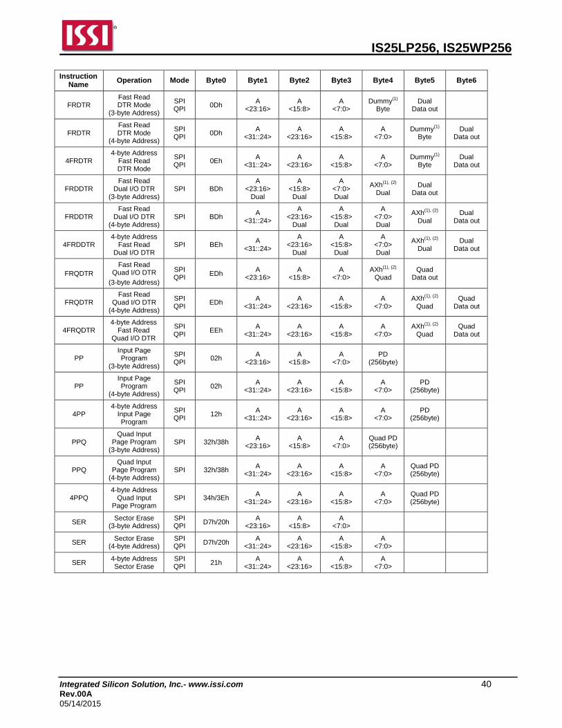
IS25LP256, IS25WP256
Integrated Silicon Solution, Inc.- www.issi.com 40 Rev.00A 05/14/2015
Instruction Name Operation Mode Byte0 Byte1 Byte2 Byte3 Byte4 Byte5 Byte6
FRDTR Fast Read DTR Mode
(3-byte Address)
SPI QPI 0Dh A
<23:16> A
<15:8> A
<7:0> Dummy(1)
Byte Dual
Data out
FRDTR Fast Read DTR Mode
(4-byte Address)
SPI QPI 0Dh A
<31::24> A
<23:16> A
<15:8> A
<7:0> Dummy(1)
Byte Dual
Data out
4FRDTR 4-byte Address
Fast Read DTR Mode
SPI QPI 0Eh A
<31::24> A
<23:16> A
<15:8> A
<7:0> Dummy(1)
Byte Dual
Data out
FRDDTR Fast Read
Dual I/O DTR (3-byte Address)
SPI BDh A
<23:16> Dual
A <15:8> Dual
A <7:0> Dual
AXh(1), (2) Dual
Dual Data out
FRDDTR Fast Read
Dual I/O DTR (4-byte Address)
SPI BDh A <31::24>
A <23:16>
Dual
A <15:8> Dual
A <7:0> Dual
AXh(1), (2) Dual
Dual Data out
4FRDDTR 4-byte Address
Fast Read Dual I/O DTR
SPI BEh A <31::24>
A <23:16>
Dual
A <15:8> Dual
A <7:0> Dual
AXh(1), (2) Dual
Dual Data out
FRQDTR Fast Read
Quad I/O DTR (3-byte Address)
SPI QPI EDh A
<23:16> A
<15:8> A
<7:0> AXh(1), (2)
Quad Quad
Data out
FRQDTR Fast Read
Quad I/O DTR (4-byte Address)
SPI QPI EDh A
<31::24> A
<23:16> A
<15:8> A
<7:0> AXh(1), (2)
Quad Quad
Data out
4FRQDTR 4-byte Address
Fast Read Quad I/O DTR
SPI QPI EEh A
<31::24> A
<23:16> A
<15:8> A
<7:0> AXh(1), (2)
Quad Quad
Data out
PP Input Page Program
(3-byte Address)
SPI QPI 02h A
<23:16> A
<15:8> A
<7:0> PD
(256byte)
PP Input Page Program
(4-byte Address)
SPI QPI 02h A
<31::24> A
<23:16> A
<15:8> A
<7:0> PD
(256byte)
4PP 4-byte Address
Input Page Program
SPI QPI 12h A
<31::24> A
<23:16> A
<15:8> A
<7:0> PD
(256byte)
PPQ Quad Input
Page Program (3-byte Address)
SPI 32h/38h A <23:16>
A <15:8>
A <7:0>
Quad PD (256byte)
PPQ Quad Input
Page Program (4-byte Address)
SPI 32h/38h A <31::24>
A <23:16>
A <15:8>
A <7:0>
Quad PD (256byte)
4PPQ 4-byte Address
Quad Input Page Program
SPI 34h/3Eh A <31::24>
A <23:16>
A <15:8>
A <7:0>
Quad PD (256byte)
SER Sector Erase (3-byte Address)
SPI QPI D7h/20h A
<23:16> A
<15:8> A
<7:0>
SER Sector Erase (4-byte Address)
SPI QPI D7h/20h A
<31::24> A
<23:16> A
<15:8> A
<7:0>
SER 4-byte Address Sector Erase
SPI QPI 21h A
<31::24> A
<23:16> A
<15:8> A
<7:0>

IS25LP256, IS25WP256
Integrated Silicon Solution, Inc.- www.issi.com 41 Rev.00A 05/14/2015
Instruction Name Operation Mode Byte0 Byte1 Byte2 Byte3 Byte4 Byte5 Byte6
BER32 (32KB)
Block Erase 32Kbyte
(3-byte Address)
SPI QPI 52h A
<23:16> A
<15:8> A
<7:0>
BER32 (32KB)
Block Erase 32Kbyte
(4-byte Address)
SPI QPI 52h A
<31::24> A
<23:16> A
<15:8> A
<7:0>
4BER32 (32KB)
4-byte Address Block Erase
32Kbyte
SPI QPI 5Ch A
<31::24> A
<23:16> A
<15:8> A
<7:0>
BER64 (64KB)
Block Erase 64Kbyte
(3-byte Address)
SPI QPI D8h A
<23:16> A
<15:8> A
<7:0>
BER64 (64KB)
Block Erase 64Kbyte
(4-byte Address)
SPI QPI D8h A
<31::24> A
<23:16> A
<15:8> A
<7:0>
BER64 (64KB)
4-byte Address Block Erase
64Kbyte
SPI QPI DCh A
<31::24> A
<23:16> A
<15:8> A
<7:0>
CER Chip Erase SPI QPI C7h/60h
WREN Write Enable SPI QPI 06h
WRDI Write Disable SPI QPI 04h
RDSR Read Status Register
SPI QPI 05h Data out
WRSR Write Status Register
SPI QPI 01h Data in
RDFR Read Function Register
SPI QPI 48h Data out
WRFR Write Function Register
SPI QPI 42h Data in
QIOEN Enter QPI mode SPI 35h
QIODI Exit QPI mode QPI F5h
PERSUS Suspend during program/erase
SPI QPI
75h/B0h/ 85h
PERRSM Resume program/erase
SPI QPI
7Ah/30h/ 8Ah
DP Deep Power Down
SPI QPI B9h
RDID, RDPD
Read ID / Release
Power Down
SPI QPI ABh XXh(3) XXh(3) XXh(3) ID7-ID0
SRPNV Set Read
Parameters (Non-Volatile)
SPI QPI 65h Data in
SRPV Set Read
Parameters (Volatile)
SPI QPI C0h/63h Data in
SERPNV Set Extended
Read Parameters (Non-Volatile)
SPI QPI 85h Data in
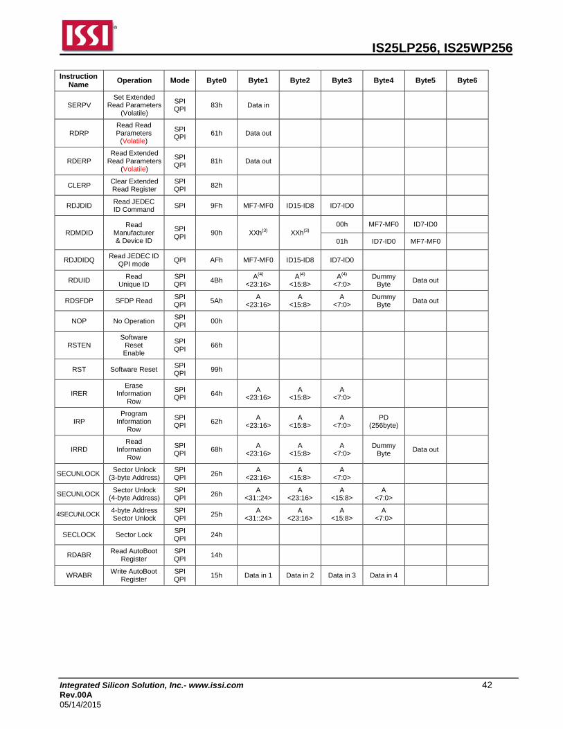
IS25LP256, IS25WP256
Integrated Silicon Solution, Inc.- www.issi.com 42 Rev.00A 05/14/2015
Instruction Name Operation Mode Byte0 Byte1 Byte2 Byte3 Byte4 Byte5 Byte6
SERPV Set Extended
Read Parameters (Volatile)
SPI QPI 83h Data in
RDRP Read Read Parameters
(Volatile)
SPI QPI 61h Data out
RDERP Read Extended
Read Parameters (Volatile)
SPI QPI 81h Data out
CLERP Clear Extended Read Register
SPI QPI 82h
RDJDID Read JEDEC ID Command SPI 9Fh MF7-MF0 ID15-ID8 ID7-ID0
RDMDID Read
Manufacturer & Device ID
SPI QPI 90h XXh(3) XXh(3)
00h MF7-MF0 ID7-ID0
01h ID7-ID0 MF7-MF0
RDJDIDQ Read JEDEC ID QPI mode QPI AFh MF7-MF0 ID15-ID8 ID7-ID0
RDUID Read Unique ID
SPI QPI 4Bh A(4)
<23:16> A(4)
<15:8> A(4)
<7:0> Dummy
Byte Data out
RDSFDP SFDP Read SPI QPI 5Ah A
<23:16> A
<15:8> A
<7:0> Dummy
Byte Data out
NOP No Operation SPI QPI 00h
RSTEN Software
Reset Enable
SPI QPI 66h
RST Software Reset SPI QPI 99h
IRER Erase
Information Row
SPI QPI 64h A
<23:16> A
<15:8> A
<7:0>
IRP Program
Information Row
SPI QPI 62h A
<23:16> A
<15:8> A
<7:0> PD
(256byte)
IRRD Read
Information Row
SPI QPI 68h A
<23:16> A
<15:8> A
<7:0> Dummy
Byte Data out
SECUNLOCK Sector Unlock (3-byte Address)
SPI QPI 26h A
<23:16> A
<15:8> A
<7:0>
SECUNLOCK Sector Unlock (4-byte Address)
SPI QPI 26h A
<31::24> A
<23:16> A
<15:8> A
<7:0>
4SECUNLOCK 4-byte Address Sector Unlock
SPI QPI 25h A
<31::24> A
<23:16> A
<15:8> A
<7:0>
SECLOCK Sector Lock SPI QPI 24h
RDABR Read AutoBoot Register
SPI QPI 14h
WRABR Write AutoBoot Register
SPI QPI 15h Data in 1 Data in 2 Data in 3 Data in 4

IS25LP256, IS25WP256
Integrated Silicon Solution, Inc.- www.issi.com 43 Rev.00A 05/14/2015
Instruction Name Operation Mode Byte0 Byte1 Byte2 Byte3 Byte4 Byte5 Byte6
RDBR Read Bank
Address Register (Volatile)
SPI QPI 16h/C8h Data out
WRBRV Write Bank
Address Register (Volatile)
SPI QPI 17h/C5h Data in
WRBRNV Write Bank
Address Register (Non-Volatile)
SPI QPI 18h Data in
EN4B Enter 4-byte Address Mode
SPI QPI B7h
EX4B Exit 4-byte Address Mode
SPI QPI 29h
RDDYB Read DYB (3-byte Address)
SPI QPI FAh A
<23:16> A
<15:8> A
<7:0> Data out
RDDYB Read DYB (4-byte Address)
SPI QPI FAh A
<31::24> A
<23:16> A
<15:8> A
<7:0> Data out
4RDDYB 4-byte Address Read DYB
SPI QPI E0h A
<31::24> A
<23:16> A
<15:8> A
<7:0> Data out
WRDYB Write DYB (3-byte Address)
SPI QPI FBh A
<23:16> A
<15:8> A
<7:0> Data in
WRDYB Write DYB (4-byte Address)
SPI QPI FBh A
<31::24> A
<23:16> A
<15:8> A
<7:0> Data in
4WRDYB 4-byte Address Write DYB
SPI QPI E1h A
<31::24> A
<23:16> A
<15:8> A
<7:0> Data in
RDPPB Read PPB (3-byte Address) SPI FCh A
<23:16> A
<15:8> A
<7:0> Data out
RDPPB Read PPB (4-byte Address) SPI FCh A
<31::24> A
<23:16> A
<15:8> A
<7:0> Data out
4RDPPB 4-byte Address Read PPB SPI E2h A
<31::24> A
<23:16> A
<15:8> A
<7:0> Data out
PGPPB Program PPB (Individually)
(3-byte Address)
SPI QPI FDh A
<23:16> A
<15:8> A
<7:0>
PGPPB Program PPB (Individually)
(4-byte Address)
SPI QPI FDh A
<31::24> A
<23:16> A
<15:8> A
<7:0>
4PGPPB 4-byte Address Program PPB (Individually)
SPI QPI E3h A
<31::24> A
<23:16> A
<15:8> A
<7:0>
ERPPB Erase PPB (as a group)
SPI QPI E4h
RDASP Read ASP SPI QPI 2Bh Data out
(2 byte)
PGASP Program ASP SPI QPI 2Fh PD
(2 byte)
RDPLB Read PPB Lock Bit
SPI QPI A7h Data out
WRPLB Write PPB Lock Bit
SPI QPI A6h
SFRZ Set FREEZE bit SPI QPI 91h
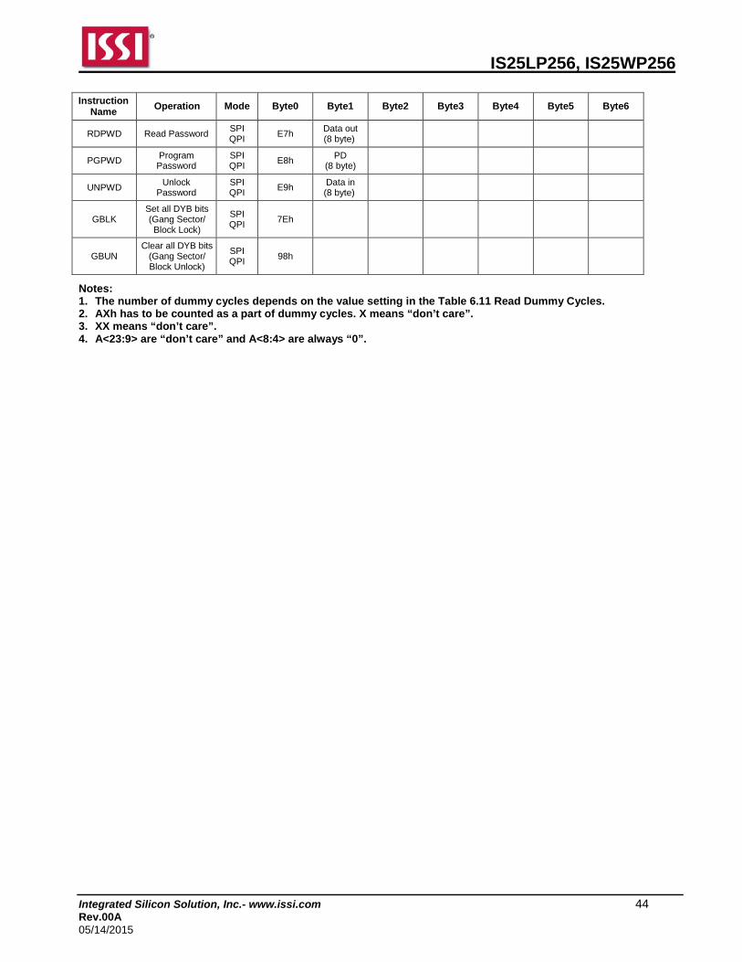
IS25LP256, IS25WP256
Integrated Silicon Solution, Inc.- www.issi.com 44 Rev.00A 05/14/2015
Instruction Name Operation Mode Byte0 Byte1 Byte2 Byte3 Byte4 Byte5 Byte6
RDPWD Read Password SPI QPI E7h Data out
(8 byte)
PGPWD Program Password
SPI QPI E8h PD
(8 byte)
UNPWD Unlock Password
SPI QPI E9h Data in
(8 byte)
GBLK Set all DYB bits (Gang Sector/ Block Lock)
SPI QPI 7Eh
GBUN Clear all DYB bits
(Gang Sector/ Block Unlock)
SPI QPI 98h
Notes: 1. The number of dummy cycles depends on the value setting in the Table 6.11 Read Dummy Cycles. 2. AXh has to be counted as a part of dummy cycles. X means “don’t care”. 3. XX means “don’t care”. 4. A<23:9> are “don’t care” and A<8:4> are always “0”.
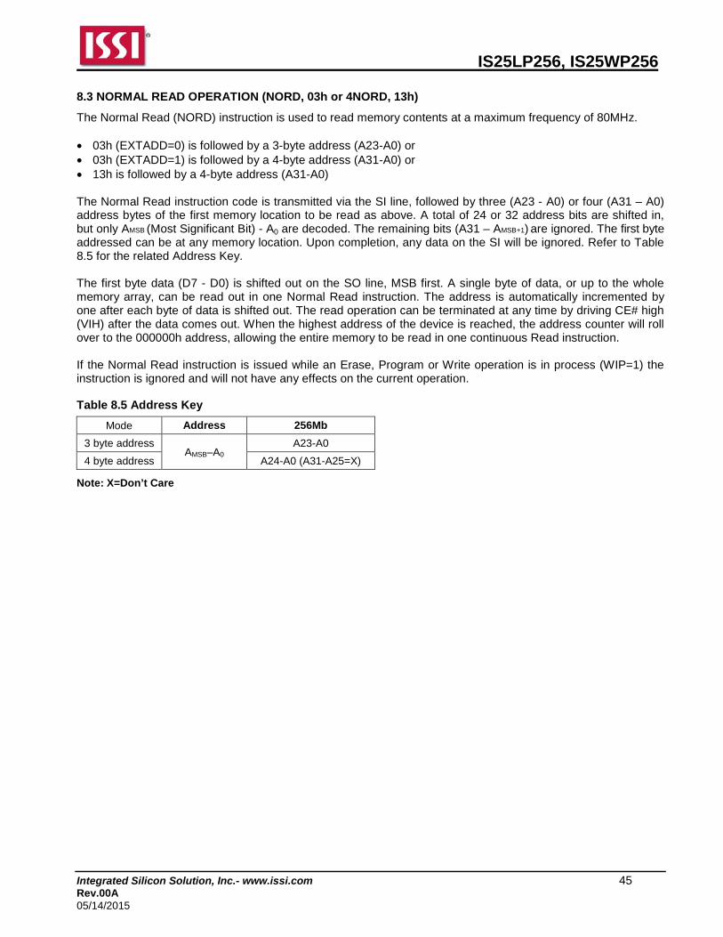
IS25LP256, IS25WP256
Integrated Silicon Solution, Inc.- www.issi.com 45 Rev.00A 05/14/2015
8.3 NORMAL READ OPERATION (NORD, 03h or 4NORD, 13h)
The Normal Read (NORD) instruction is used to read memory contents at a maximum frequency of 80MHz. • 03h (EXTADD=0) is followed by a 3-byte address (A23-A0) or • 03h (EXTADD=1) is followed by a 4-byte address (A31-A0) or • 13h is followed by a 4-byte address (A31-A0) The Normal Read instruction code is transmitted via the SI line, followed by three (A23 - A0) or four (A31 – A0) address bytes of the first memory location to be read as above. A total of 24 or 32 address bits are shifted in, but only AMSB (Most Significant Bit) - A0 are decoded. The remaining bits (A31 – AMSB+1) are ignored. The first byte addressed can be at any memory location. Upon completion, any data on the SI will be ignored. Refer to Table 8.5 for the related Address Key. The first byte data (D7 - D0) is shifted out on the SO line, MSB first. A single byte of data, or up to the whole memory array, can be read out in one Normal Read instruction. The address is automatically incremented by one after each byte of data is shifted out. The read operation can be terminated at any time by driving CE# high (VIH) after the data comes out. When the highest address of the device is reached, the address counter will roll over to the 000000h address, allowing the entire memory to be read in one continuous Read instruction. If the Normal Read instruction is issued while an Erase, Program or Write operation is in process (WIP=1) the instruction is ignored and will not have any effects on the current operation. Table 8.5 Address Key
Mode Address 256Mb
3 byte address AMSB–A0
A23-A0
4 byte address A24-A0 (A31-A25=X)
Note: X=Don’t Care

IS25LP256, IS25WP256
Integrated Silicon Solution, Inc.- www.issi.com 46 Rev.00A 05/14/2015
Figure 8.1 Normal Read Sequence (03h [EXTADD=0], 3-byte address)
7 6
CE#
SCK
SI
5 3 2SO 4 1 0
Data Out 1
Instruction = 03h 23
CE#
SCK
SI 3 2
SO
1 0
3-byte Address
High Impedance
22 21 ...
0 1 2 3 4 5 6 7 8 9 10 ... 28 29 30 31
32 33 34 35 36 37 38 39 40 41 42 43 44 45 46 47
Mode 3
Mode 0
...
7 6 5 3 24 1 0tV
Data Out 2
...

IS25LP256, IS25WP256
Integrated Silicon Solution, Inc.- www.issi.com 47 Rev.00A 05/14/2015
Figure 8.2 Normal Read Sequence (03h [EXTADD=1] or 13h, 4-byte address)
Instruction = 03h/13h
4-byte Address
36 37 38 39
40 41 42 43 44 45 46 47 48 49 50 51 52 53 54 55 ...
7 6
CE#
SCK
SI
5 3 2SO 4 1 0
Data Out 1
23
CE#
SCK
SI 3 2
SO
1 0
High Impedance
22 21 ...
0 1 2 3 4 5 6 7 8 9 10 ...Mode 3
Mode 0
7 6 5 3 24 1 0tV
Data Out 2
...

IS25LP256, IS25WP256
Integrated Silicon Solution, Inc.- www.issi.com 48 Rev.00A 05/14/2015
8.4 FAST READ OPERATION (FRD, 0Bh or 4FRD, 0Ch)
The Fast Read (FRD, 4FRD) instruction is used to read memory data at up to a 166MHz clock. • 0Bh (EXTADD=0) is followed by a 3-byte address (A23-A0) or • 0Bh (EXTADD=1) is followed by a 4-byte address (A31-A0) or • 0Ch is followed by a 4-byte address (A31-A0) The Fast Read instruction code is followed by three or four address bytes as above and dummy cycles (configurable, default is 8 clocks), transmitted via the SI line, with each bit latched-in during the rising edge of SCK. Then the first data byte from the address is shifted out on the SO line, with each bit shifted out at a maximum frequency fCT, during the falling edge of SCK. The first byte addressed can be at any memory location. The address is automatically incremented by one after each byte of data is shifted out. When the highest address is reached, the address counter will roll over to the 000000h address, allowing the entire memory to be read with a single Fast Read instruction. The Fast Read instruction is terminated by driving CE# high (VIH). If the Fast Read instruction is issued while an Erase, Program or Write cycle is in process (WIP=1) the instruction is ignored without affecting the current cycle.

IS25LP256, IS25WP256
Integrated Silicon Solution, Inc.- www.issi.com 49 Rev.00A 05/14/2015
Figure 8.3 Fast Read Sequence (0Bh [EXTADD=0], 3-byte address)
Instruction = 0Bh
3-byte Address
28 29 30 31
32 33 34 35 36 37 38 39 40 41 42 43 44 45 46 47 ...
7 6
CE#
SCK
SI
5 3 2SO 4 1
Data Out
31
CE#
SCK
SI 3 2
SO
1 0
High Impedance
30 29 ...
0 1 2 3 4 5 6 7 8 9 10 ...Mode 3
Mode 0
tV
Dummy Cycles
0 ...
Note: Dummy cycles depends on Read Parameter setting. Detailed information in Table 6.11 Read Dummy Cycles.
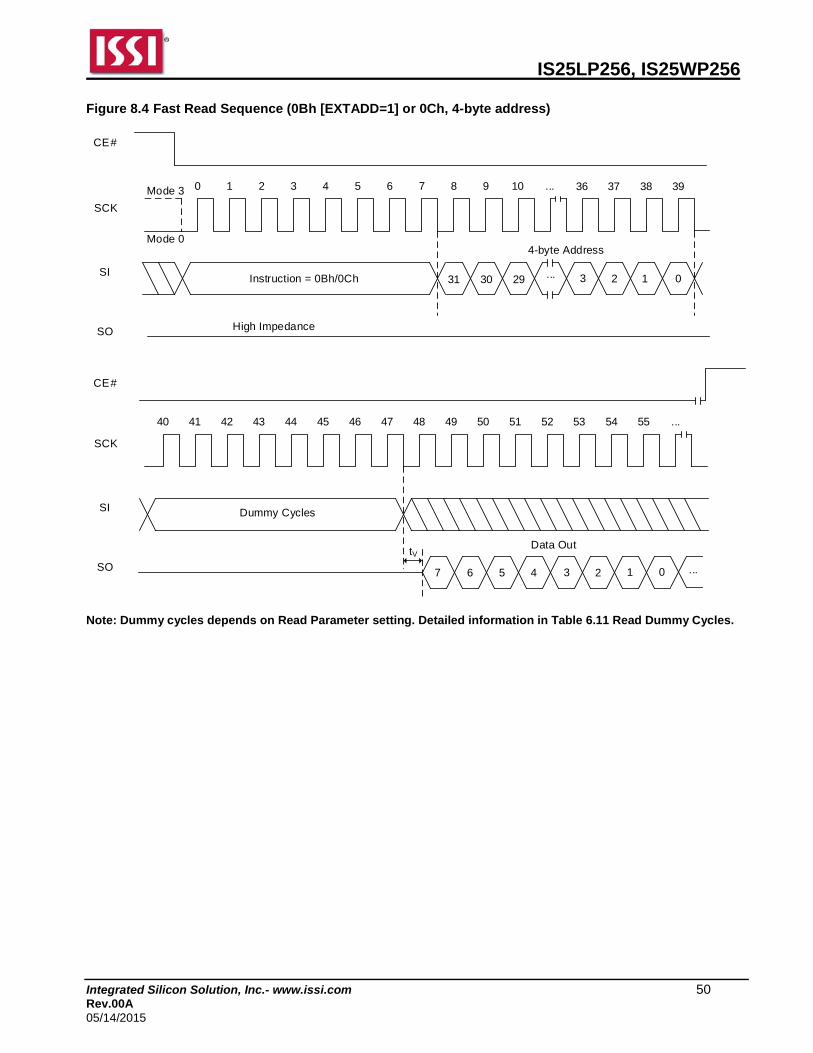
IS25LP256, IS25WP256
Integrated Silicon Solution, Inc.- www.issi.com 50 Rev.00A 05/14/2015
Figure 8.4 Fast Read Sequence (0Bh [EXTADD=1] or 0Ch, 4-byte address)
7 6
CE#
SCK
SI
5 3 2SO 4 1
Data Out
Instruction = 0Bh/0Ch 31
CE#
SCK
SI 3 2
SO
1 0
4-byte Address
High Impedance
30 29 ...
0 1 2 3 4 5 6 7 8 9 10 ...Mode 3
Mode 0
tV
Dummy Cycles
36 37 38 39
40 41 42 43 44 45 46 47 48 49 50 51 52 53 54 55 ...
0 ...
Note: Dummy cycles depends on Read Parameter setting. Detailed information in Table 6.11 Read Dummy Cycles.

IS25LP256, IS25WP256
Integrated Silicon Solution, Inc.- www.issi.com 51 Rev.00A 05/14/2015
FAST READ QPI OPERATION (FRD QPI, 0Bh or 4FRD QPI, 0Ch)
The Fast Read QPI (FRD QPI) instruction is used to read memory data at up to a 166MHz clock. • 0Bh (EXTADD=0) is followed by a 3-byte address (A23-A0) or • 0Bh (EXTADD=1) is followed by a 4-byte address (A31-A0) or • 0Ch is followed by a 4-byte address (A31-A0) The Fast Read QPI instruction code (2 clocks) is followed by three (6 clocks) or four (8 clocks) address bytes as above and 6 dummy cycles (configurable, default is 6 clocks), transmitted via the IO3, IO2, IO1 and IO0 lines, with each bit latched-in during the rising edge of SCK. Then the first data byte addressed is shifted out on the IO3, IO2, IO1 and IO0 lines, with each bit shifted out at a maximum frequency fCT, during the falling edge of SCK. The first byte addressed can be at any memory location. The address is automatically incremented by one after each byte of data is shifted out. When the highest address is reached, the address counter will roll over to the 000000h address, allowing the entire memory to be read with a single Fast Read QPI instruction. The Fast Read QPI instruction is terminated by driving CE# high (VIH). If the Fast Read QPI instruction is issued while an Erase, Program or Write cycle is in process (WIP=1) the instruction is ignored without affecting the current cycle. The Fast Read QPI sequence is also applied to the commands in the following table 8.6. However, only 3-byte address mode QPI sequence is applied for RDUID, RDSFDP, and IRRD commands. Table 8.6 Instructions that Fast Read QPI sequence is applied to
Instruction Name Operation Hex Code
FRQIO Fast Read Quad I/O EBh
RDUID Read Unique ID 4Bh
RDSFDP SFDP Read 5Ah
IRRD Read Information Row 68h
Figure 8.5 Fast Read QPI Sequence (0Bh [EXTADD=0], 3-byte address)
0Bh
CE#
SCK
IO[3:0]
6 Dummy Cycles3-byte Address
0 1 2 3 4 5 6 7 8 9 ... 13 14 15 16 17Mode 3
Mode 0
23:20 7:4 3:0 7:4 3:0
Data 1 Data 2
19:16 15:12 11:8 7:4 3:0
...
tV
...
Instruction
Note: Number of dummy cycles depends on Read Parameter setting. Detailed information in Table 6.11 Read
Dummy Cycles.

IS25LP256, IS25WP256
Integrated Silicon Solution, Inc.- www.issi.com 52 Rev.00A 05/14/2015
Figure 8.6 Fast Read QPI Sequence (0Bh [EXTADD=1] or 0Ch, 4-byte address)
0Bh/0Ch
CE#
SCK
IO[3:0]
6 Dummy Cycles4-byte Address
0 1 2 3 4 5 6 7 8 9 10 11 ... 15 16 17Mode 3
Mode 0
31:28 7:4 3:0
Data 1
27:24 15:12 11:8 7:4 3:0
...
tV
...
Instruction
23:20 19:16
Note: Number of dummy cycles depends on Read Parameter setting. Detailed information in Table 6.11 Read
Dummy Cycles.
8.5 HOLD OPERATION
HOLD# is used in conjunction with CE# to select the device. When the device is selected and a serial sequence is underway, HOLD# can be used to pause the serial communication with the master device without resetting the serial sequence. To pause, HOLD# is brought low while the SCK signal is low. To resume serial communication, HOLD# is brought high while the SCK signal is low (SCK may still toggle during HOLD). Inputs to SI will be ignored while SO is in the high impedance state, during HOLD.
Note: HOLD is not supported in DTR mode or with QE=1 or when RESET# is selected for the HOLD# or RESET# pin. Timing graph can be referenced in AC Parameters Figure 9.4.

IS25LP256, IS25WP256
Integrated Silicon Solution, Inc.- www.issi.com 53 Rev.00A 05/14/2015
8.6 FAST READ DUAL I/O OPERATION (FRDIO, BBh or 4FRDIO, BCh)
The Fast Read Dual I/O (FRDIO, 4FRDIO) instruction allows the address bits to be input two bits at a time. This may allow for code to be executed directly from the SPI in some applications. • BBh (EXTADD=0) is followed by a 3-byte address (A23-A0) or • BBh (EXTADD=1) is followed by a 4-byte address (A31-A0) or • BCh is followed by a 4-byte address (A31-A0) The FRDIO/4FRDIO instruction code is followed by three or four address bytes as above and dummy cycles (configurable, default is 4 clocks), transmitted via the IO1 and IO0 lines, with each pair of bits latched-in during the rising edge of SCK. The address MSB is input on IO1, the next bit on IO0, and this shift pattern continues to alternate between the two lines. Depending on the usage of AX read operation mode, a mode byte may be located after address input. The first data byte addressed is shifted out on the IO1 and IO0 lines, with each pair of bits shifted out at a maximum frequency fCT, during the falling edge of SCK. The first bit (MSB) is output on IO1, while simultaneously the second bit is output on IO0. Figures 8.7 and 8.8 illustrates the timing sequence. The first byte addressed can be at any memory location. The address is automatically incremented by one after each byte of data is shifted out. When the highest address is reached, the address counter will roll over to the 000000h address, allowing the entire memory to be read with a single FRDIO/4FRDIO instruction. The FRDIO/4FRDIO instruction is terminated by driving CE# high (VIH). The device supports the AX read operation by applying mode bits during dummy period. Mode bits consist of 8 bits, such as M7 to M0. Four cycles after address input are reserved for Mode bits in FRDIO/4FRDIO execution. M7 to M4 are important for enabling this mode. M3 to M0 become don’t care for future use. When M[7:4]=1010(Ah), it enables the AX read operation and subsequent FRDIO/4FRDIO execution skips command code. It saves cycles as described in Figures 8.9 and 8.10. When the code is different from AXh (where X is don’t care), the device exits the AX read operation. After finishing the read operation, device becomes ready to receive a new command. SPI or QPI mode configuration retains the prior setting. Mode bit must be applied during dummy cycles. Number of dummy cycles in Table 6.11 includes number of mode bit cycles. If dummy cycles are configured as 4 cycles, data output will start right after mode bit is applied. If the FRDIO/4FRDIO instruction is issued while an Erase, Program or Write cycle is in process (WIP=1) the instruction is ignored and will not affect the current cycle.

IS25LP256, IS25WP256
Integrated Silicon Solution, Inc.- www.issi.com 54 Rev.00A 05/14/2015
Figure 8.7 Fast Read Dual I/O Sequence (BBh [EXTADD=0], 3-byte address)
7 5 3 7 51 3 1
Data Out 1
Instruction = BBh 22
CE#
SCK
2 0 6 4
3-byte Address
High Impedance
20 18 ...
0 1 2 3 4 5 6 7 8 9 10 ... 18 19 20 21
22 23 24 25 26 27 28 29 30 31 32 33 34 35 36 37
Mode 3
Mode 0
...
tV
23 3 1 7 521 19 ...
IO0
IO1
3 1
2 0 6 4 2 6 40 2 0
4 Dummy Cycles
7 5 3 1
6 4 2 0
7 5 ...
6 4 ...
CE#
SCK
IO0
IO1
Data Out 2 Data Out 3
Mode Bits
Mode Bits Notes: 1. If the mode bits=AXh (where X is don’t care), it can execute the AX read mode (without command). When the
mode bits are different from AXh, the device exits the AX read operation. 2. Number of dummy cycles depends on clock speed. Detailed information in Table 6.11 Read Dummy Cycles. 3. Sufficient dummy cycles are required to avoid I/O contention. If the number of dummy cycles and AX bits cycles
are same, then X should be Hi-Z.

IS25LP256, IS25WP256
Integrated Silicon Solution, Inc.- www.issi.com 55 Rev.00A 05/14/2015
Figure 8.8 Fast Read Dual I/O Sequence (BBh [EXTADD=1] or BCh, 4-byte address)
4-byte Address
22 23 24 25
26 27 28 29 30 31 32 33 34 35 36 37 38 39 36 41 ...
Instruction = BBh/BCh
7 5 3 7 51 3 1
Data Out 1
22
CE#
SCK
2 0 6 4
High Impedance
20 18 ...
0 1 2 3 4 5 6 7 8 9 10 ...Mode 3
Mode 0
tV
23 3 1 7 521 19 ...
IO0
IO1
3 1
2 0 6 4 2 6 40 2 0
4 Dummy Cycles
7 5 3 1
6 4 2 0
7 5 ...
6 4 ...
CE#
SCK
IO0
IO1
Data Out 2 Data Out 3
Mode Bits
Mode Bits Notes: 1. If the mode bits=AXh (where X is don’t care), it can execute the AX read mode (without command). When the
mode bits are different from AXh, the device exits the AX read operation. 2. Number of dummy cycles depends on clock speed. Detailed information in Table 6.11 Read Dummy Cycles. 3. Sufficient dummy cycles are required to avoid I/O contention. If the number of dummy cycles and AX bits cycles
are same, then X should be Hi-Z.
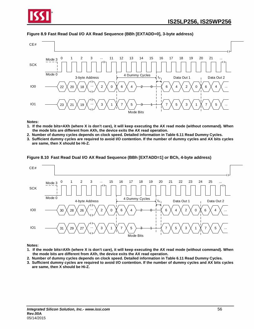
IS25LP256, IS25WP256
Integrated Silicon Solution, Inc.- www.issi.com 56 Rev.00A 05/14/2015
Figure 8.9 Fast Read Dual I/O AX Read Sequence (BBh [EXTADD=0], 3-byte address)
22
CE#
SCK
2 0
3-byte Address
20 18 ...
0 1 2 3 ... 11 12 13 14 15 16 17 18 19 20 21Mode 3
Mode 0
23 3 121 19 ...
IO0
IO1
4 Dummy Cycles
6
7
6 4
7 5
2 0
3 1
Data Out 1tV
6 4
7 5
2 0
3 1
4
5
Mode Bits
...
...
Data Out 2
...
Notes: 1. If the mode bits=AXh (where X is don’t care), it will keep executing the AX read mode (without command). When
the mode bits are different from AXh, the device exits the AX read operation. 2. Number of dummy cycles depends on clock speed. Detailed information in Table 6.11 Read Dummy Cycles. 3. Sufficient dummy cycles are required to avoid I/O contention. If the number of dummy cycles and AX bits cycles
are same, then X should be Hi-Z. Figure 8.10 Fast Read Dual I/O AX Read Sequence (BBh [EXTADD=1] or BCh, 4-byte address)
30
CE#
SCK
2 0
4-byte Address
28 26 ...
0 1 2 3 ... 15 16 17 18 19 20 21 22 23 24 25Mode 3
Mode 0
31 3 129 27 ...
IO0
IO1
4 Dummy Cycles
6
7
6 4
7 5
2 0
3 1
Data Out 1tV
6 4
7 5
2 0
3 1
4
5
Mode Bits
...
...
Data Out 2
...
Notes: 1. If the mode bits=AXh (where X is don’t care), it will keep executing the AX read mode (without command). When
the mode bits are different from AXh, the device exits the AX read operation. 2. Number of dummy cycles depends on clock speed. Detailed information in Table 6.11 Read Dummy Cycles. 3. Sufficient dummy cycles are required to avoid I/O contention. If the number of dummy cycles and AX bits cycles
are same, then X should be Hi-Z.

IS25LP256, IS25WP256
Integrated Silicon Solution, Inc.- www.issi.com 57 Rev.00A 05/14/2015
8.7 FAST READ DUAL OUTPUT OPERATION (FRDO, 3Bh or 4FRDO, 3Ch)
The FRDO/4FRDO instruction is used to read memory data on two output pins each at up to a 166MHz clock. • 3Bh (EXTADD=0) is followed by a 3-byte address (A23-A0) or • 3Bh (EXTADD=1) is followed by a 4-byte address (A31-A0) or • 3Ch is followed by a 4-byte address (A31-A0) The FRDO/4FRDO instruction code is followed by three or four address bytes as above and dummy cycles (configurable, default is 8 clocks), transmitted via the IO0 line, with each bit latched-in during the rising edge of SCK. Then the first data byte addressed is shifted out on the IO1 and IO0 lines, with each pair of bits shifted out at a maximum frequency fCT, during the falling edge of SCK. The first bit (MSB) is output on IO1. Simultaneously, the second bit is output on IO0. The first byte addressed can be at any memory location. The address is automatically incremented by one after each byte of data is shifted out. When the highest address is reached, the address counter will roll over to the 000000h address, allowing the entire memory to be read with a single FRDO/4FRDO instruction. The instruction FRDO/4FRDO is terminated by driving CE# high (VIH). If the FRDO/4FRDO instruction is issued while an Erase, Program or Write cycle is in process (WIP=1) the instruction is ignored and will not have any effects on the current cycle.

IS25LP256, IS25WP256
Integrated Silicon Solution, Inc.- www.issi.com 58 Rev.00A 05/14/2015
Figure 8.11 Fast Read Dual Output Sequence (3Bh [EXTADD=0], 3-byte address)
CE#
SCK
7 5
Data Out 1
Instruction = 3Bh 23
CE#
SCK
3 2 1 0
3-byte Address
High Impedance
22 21 ...
0 1 2 3 4 5 6 7 8 9 10 ... 28 29 30 31
32 33 34 35 36 37 38 39 40 41 42 43 44 45 46 47
Mode 3
Mode 0
...
tV
IO0
IO1
6 4
3 1 7 5
2 0 6 4
3 1 ...
2 0 ...
Data Out 2
IO0
IO1
8 Dummy Cycles
Note: Dummy cycles depends on Read Parameter setting. Detailed information in Table 6.11 Read Dummy Cycles.
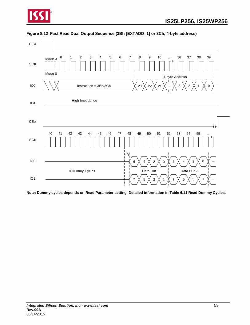
IS25LP256, IS25WP256
Integrated Silicon Solution, Inc.- www.issi.com 59 Rev.00A 05/14/2015
Figure 8.12 Fast Read Dual Output Sequence (3Bh [EXTADD=1] or 3Ch, 4-byte address)
Instruction = 3Bh/3Ch
4-byte Address
36 37 38 39
40 41 42 43 44 45 46 47 48 49 50 51 52 53 54 55 ...
CE#
SCK
7 5
Data Out 1
23
CE#
SCK
3 2 1 0
High Impedance
22 21 ...
0 1 2 3 4 5 6 7 8 9 10 ...Mode 3
Mode 0
tV
IO0
IO1
6 4
3 1 7 5
2 0 6 4
3 1 ...
2 0 ...
Data Out 2
IO0
IO1
8 Dummy Cycles
Note: Dummy cycles depends on Read Parameter setting. Detailed information in Table 6.11 Read Dummy Cycles.
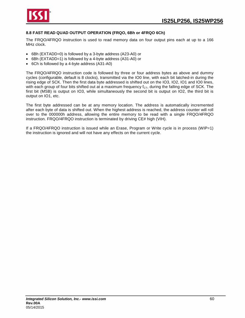
IS25LP256, IS25WP256
Integrated Silicon Solution, Inc.- www.issi.com 60 Rev.00A 05/14/2015
8.8 FAST READ QUAD OUTPUT OPERATION (FRQO, 6Bh or 4FRQO 6Ch)
The FRQO/4FRQO instruction is used to read memory data on four output pins each at up to a 166 MHz clock. • 6Bh (EXTADD=0) is followed by a 3-byte address (A23-A0) or • 6Bh (EXTADD=1) is followed by a 4-byte address (A31-A0) or • 6Ch is followed by a 4-byte address (A31-A0) The FRQO/4FRQO instruction code is followed by three or four address bytes as above and dummy cycles (configurable, default is 8 clocks), transmitted via the IO0 line, with each bit latched-in during the rising edge of SCK. Then the first data byte addressed is shifted out on the IO3, IO2, IO1 and IO0 lines, with each group of four bits shifted out at a maximum frequency fCT, during the falling edge of SCK. The first bit (MSB) is output on IO3, while simultaneously the second bit is output on IO2, the third bit is output on IO1, etc. The first byte addressed can be at any memory location. The address is automatically incremented after each byte of data is shifted out. When the highest address is reached, the address counter will roll over to the 000000h address, allowing the entire memory to be read with a single FRQO/4FRQO instruction. FRQO/4FRQO instruction is terminated by driving CE# high (VIH). If a FRQO/4FRQO instruction is issued while an Erase, Program or Write cycle is in process (WIP=1) the instruction is ignored and will not have any effects on the current cycle.

IS25LP256, IS25WP256
Integrated Silicon Solution, Inc.- www.issi.com 61 Rev.00A 05/14/2015
Figure 8.13 Fast Read Quad Output Sequence (6Bh [EXTADD=0], 3-byte address)
CE#
SCK
5 1
Data Out 1
Instruction = 6Bh 23
CE#
SCK
3 2 1 0
3-byte Address
High Impedance
22 21 ...
0 1 2 3 4 5 6 7 8 9 10 ... 28 29 30 31
32 33 34 35 36 37 38 39 40 41 42 43 44 45 46 47
Mode 3
Mode 0
...
tV
IO0
IO1
4 0
5 1 5 1
4 0 4 0
5 1 ...
4 0 ...IO0
IO1
8 Dummy Cycles
High ImpedanceIO2
High ImpedanceIO3
7 3
6 2
7 3 7 3
6 2 6 2
7 3 ...
6 2 ...IO2
IO3
Data Out 2 Data Out 3 Data Out 4
Note: Dummy cycles depends on Read Parameter setting. Detailed information in Table 6.11 Read Dummy Cycles.
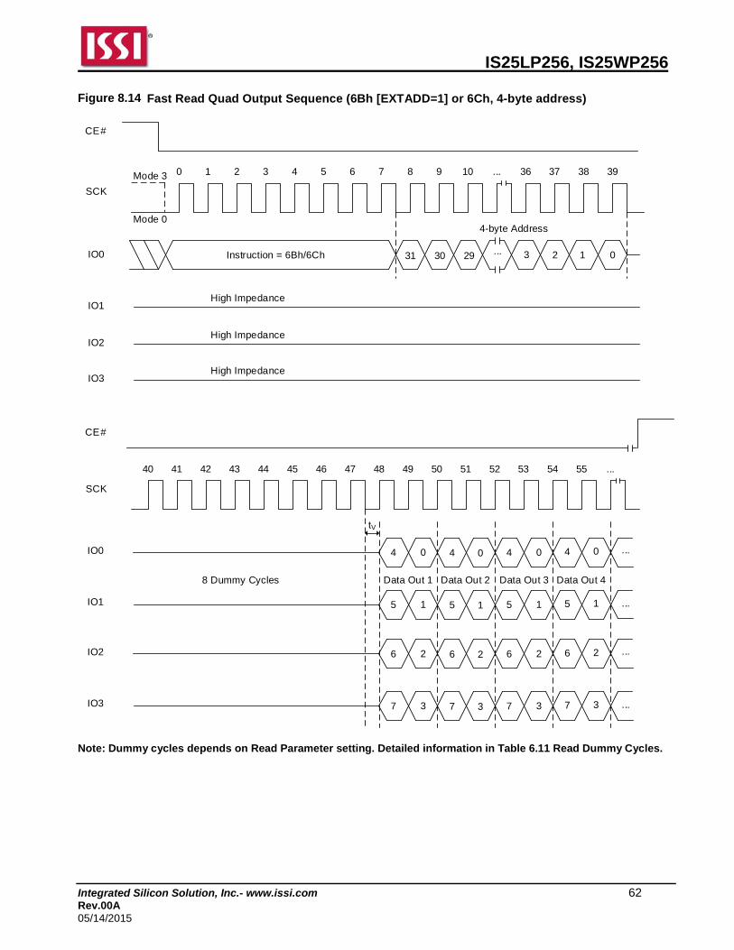
IS25LP256, IS25WP256
Integrated Silicon Solution, Inc.- www.issi.com 62 Rev.00A 05/14/2015
Figure 8.14 Fast Read Quad Output Sequence (6Bh [EXTADD=1] or 6Ch, 4-byte address)
CE#
0 1 2 3 4 5 6 7 8 9 10 ... 36 37 38 39
40 41 42 43 44 45 46 47 48 49 50 51 52 53 54 55
Mode 3
...
CE#
Instruction = 6Bh/6Ch 31
SCK
3 2 1 0
4-byte Address
High Impedance
30 29 ...
Mode 0
IO0
IO1
High ImpedanceIO2
High ImpedanceIO3
SCK
5 1
Data Out 1
tV
4 0
5 1 5 1
4 0 4 0
5 1 ...
4 0 ...IO0
IO1
8 Dummy Cycles
7 3
6 2
7 3 7 3
6 2 6 2
7 3 ...
6 2 ...IO2
IO3
Data Out 2 Data Out 3 Data Out 4
Note: Dummy cycles depends on Read Parameter setting. Detailed information in Table 6.11 Read Dummy Cycles.

IS25LP256, IS25WP256
Integrated Silicon Solution, Inc.- www.issi.com 63 Rev.00A 05/14/2015
8.9 FAST READ QUAD I/O OPERATION (FRQIO, EBh or 4FRQIO, ECh)
The FRQIO/4FRQIO instruction allows the address bits to be input four bits at a time. This may allow for code to be executed directly from the SPI in some applications. • EBh (EXTADD=0) is followed by a 3-byte address (A23-A0) or • EBh (EXTADD=1) is followed by a 4-byte address (A31-A0) or • ECh is followed by a 4-byte address (A31-A0) The FRQIO/4FRQIO instruction code is followed by three or four address bytes as above and dummy cycles (configurable, default is 6 clocks), transmitted via the IO3, IO2, IO1 and IO0 lines, with each group of four bits latched-in during the rising edge of SCK. The address of MSB inputs on IO3, the next bit on IO2, the next bit on IO1, the next bit on IO0, and continue to shift in alternating on the four. Depending on the usage of AX read operation mode, a mode byte may be located after address input. The first data byte addressed is shifted out on the IO3, IO2, IO1 and IO0 lines, with each group of four bits shifted out at a maximum frequency fCT, during the falling edge of SCK. The first bit (MSB) is output on IO3, while simultaneously the second bit is output on IO2, the third bit is output on IO1, etc. Figures 8.15 and 8.16 illustrates the timing sequence. The first byte addressed can be at any memory location. The address is automatically incremented after each byte of data is shifted out. When the highest address is reached, the address counter will roll over to the 000000h address, allowing the entire memory to be read with a single FRQIO/4FRQIO instruction. FRQIO/4FRQIO instruction is terminated by driving CE# high (VIH). The device supports the AX read operation by applying mode bits during dummy period. Mode bits consist of 8 bits, such as M7 to M0. Two cycles after address input are reserved for Mode bits in FRQIO/4FRQIO execution. M7 to M4 are important for enabling this mode. M3 to M0 become don’t care for future use. When M[7:4]=1010(Ah), it enables the AX read operation and subsequent FRQIO/4FRQIO execution skips command code. It saves cycles as described in Figures 8.17 and 8.18. When the code is different from AXh (where X is don’t care), the device exits the AX read operation. After finishing the read operation, device becomes ready to receive a new command. SPI or QPI mode configuration retains the prior setting. Mode bit must be applied during dummy cycles. Number of dummy cycles in Table 6.11 includes number of mode bit cycles. If dummy cycles are configured as 6 cycles, data output will start right after mode bits and 4 additional dummy cycles are applied. If the FRQIO/4FRQIO instruction is issued while an Erase, Program or Write cycle is in process (WIP=1) the instruction is ignored and will not have any effects on the current cycle.
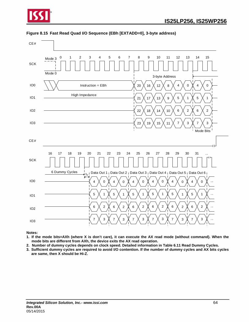
IS25LP256, IS25WP256
Integrated Silicon Solution, Inc.- www.issi.com 64 Rev.00A 05/14/2015
Figure 8.15 Fast Read Quad I/O Sequence (EBh [EXTADD=0], 3-byte address)
CE#
SCK
5 1
Data Out 1
Instruction = EBh 20
CE#
SCK
4 0 4 0
3-byte Address
High Impedance
16 12 8
0 1 2 3 4 5 6 7 8 9 10 11 12 13 14 15
16 17 18 19 20 21 22 23 24 25 26 27 28 29 30 31
Mode 3
Mode 0
...
tV
IO0
IO1
4 0
5 1 5 1
4 0 4 0
5 1
4 0IO0
IO1
21 5 1 5 117 13 9
22 6 2 6 218 14 10
23 7 3 7 319 15 11
Mode Bits
IO2
IO3
6 2 6 2 6 2 6 2
7 3 7 3 7 3 7 3
Data Out 2 Data Out 3 Data Out 4
IO2
IO3
1
0
5 1 ...
4 0 ...
2 6 2 ...
3 7 3 ...
5
4
6
7
6 Dummy Cycles Data Out 5 Data Out 6
Notes: 1. If the mode bits=AXh (where X is don’t care), it can execute the AX read mode (without command). When the
mode bits are different from AXh, the device exits the AX read operation. 2. Number of dummy cycles depends on clock speed. Detailed information in Table 6.11 Read Dummy Cycles. 3. Sufficient dummy cycles are required to avoid I/O contention. If the number of dummy cycles and AX bits cycles
are same, then X should be Hi-Z.
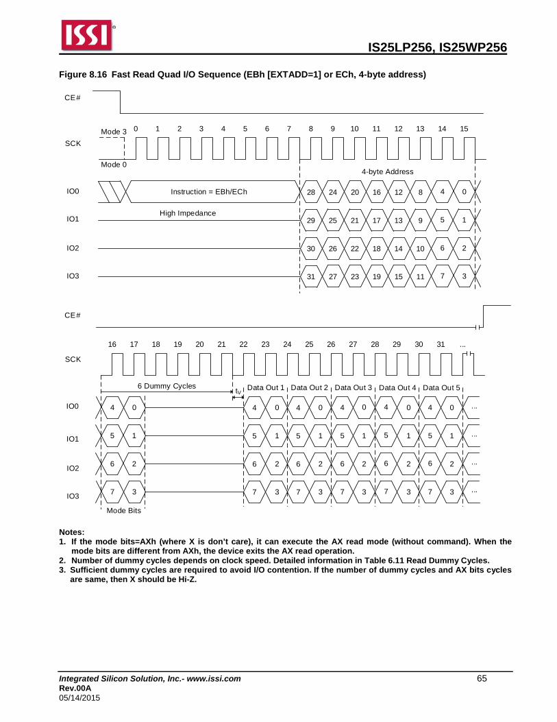
IS25LP256, IS25WP256
Integrated Silicon Solution, Inc.- www.issi.com 65 Rev.00A 05/14/2015
Figure 8.16 Fast Read Quad I/O Sequence (EBh [EXTADD=1] or ECh, 4-byte address)
CE#
SCK
5 1
Data Out 1
Instruction = EBh/ECh 20
CE#
SCK
4 028 24
4-byte Address
High Impedance
16 12 8
0 1 2 3 4 5 6 7 8 9 10 11 12 13 14 15
16 17 18 19 20 21 22 23 24 25 26 27 28 29 30 31
Mode 3
Mode 0
...
tV
IO0
IO1
4 0
5 1
4 0
5 1
4 0IO0
IO1
21 5 129 25 17 13 9
22 6 230 26 18 14 10
23 7 331 27 19 15 11
IO2
IO3
6 2 6 2 6 2
7 3 7 3 7 3
Data Out 2 Data Out 3
IO2
IO3
1
0
5 1 ...
4 0 ...
2 6 2 ...
3 7 3 ...
5
4
6
7
6 Dummy Cycles Data Out 4 Data Out 5
4 0
5 1
6 2
7 3
Mode Bits Notes: 1. If the mode bits=AXh (where X is don’t care), it can execute the AX read mode (without command). When the
mode bits are different from AXh, the device exits the AX read operation. 2. Number of dummy cycles depends on clock speed. Detailed information in Table 6.11 Read Dummy Cycles. 3. Sufficient dummy cycles are required to avoid I/O contention. If the number of dummy cycles and AX bits cycles
are same, then X should be Hi-Z.

IS25LP256, IS25WP256
Integrated Silicon Solution, Inc.- www.issi.com 66 Rev.00A 05/14/2015
Figure 8.17 Fast Read Quad I/O AX Read Sequence (EBh [EXTADD=0], 3-byte address)
20
CE#
SCK
4 0 4 0
3-byte Address
16 12 8
0 1 2 3 4 5 6 7 8 9 10 11 12 13 14 15Mode 3
Mode 0
IO0
IO1 21 5 1 5 117 13 9
22 6 2 6 218 14 10
23 7 3 7 319 15 11
Mode Bits
IO2
IO3
5 1
4 0
5 1
4 0
6 2 6 2
7 3 7 3
...
...
...
...
Data Out 1 Data Out 2
...
tV
6 Dummy Cycles
Notes: 1. If the mode bits=AXh (where X is don’t care), it will keep executing the AX read mode (without command). When
the mode bits are different from AXh, the device exits the AX read operation. 2. Number of dummy cycles depends on clock speed. Detailed information in Table 6.11 Read Dummy Cycles. 3. Sufficient dummy cycles are required to avoid I/O contention. If the number of dummy cycles and AX bits cycles
are same, then X should be Hi-Z.
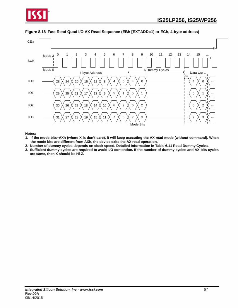
IS25LP256, IS25WP256
Integrated Silicon Solution, Inc.- www.issi.com 67 Rev.00A 05/14/2015
Figure 8.18 Fast Read Quad I/O AX Read Sequence (EBh [EXTADD=1] or ECh, 4-byte address)
20
CE#
SCK
4 0 4 0
4-byte Address
16 12 8
0 1 2 3 4 5 6 7 8 9 10 11 12 13 14 15Mode 3
Mode 0
IO0
IO1 21 5 1 5 117 13 9
22 6 2 6 218 14 10
23 7 3 7 319 15 11
IO2
IO3
5 1
4 0
6 2
7 3
...
...
...
...
Data Out 1
...
tV
6 Dummy Cycles
28 24
29 25
30 26
31 27
Mode Bits
Notes: 1. If the mode bits=AXh (where X is don’t care), it will keep executing the AX read mode (without command). When
the mode bits are different from AXh, the device exits the AX read operation. 2. Number of dummy cycles depends on clock speed. Detailed information in Table 6.11 Read Dummy Cycles. 3. Sufficient dummy cycles are required to avoid I/O contention. If the number of dummy cycles and AX bits cycles
are same, then X should be Hi-Z.

IS25LP256, IS25WP256
Integrated Silicon Solution, Inc.- www.issi.com 68 Rev.00A 05/14/2015
FAST READ QUAD I/O QPI OPERATION (FRQIO QPI, EBh or 4FRQIO QPI, ECh)
The FRQIO/4FRQIO QPI instruction is used to read memory data at up to a 166MHz clock. The FRQIO/4FRQIO QPI instruction utilizes all four IO lines to input the instruction code so that only two clocks are required, while the FRQIO/4FRQIO instruction requires that the byte-long instruction code is shifted into the device only via IO0 line in eight clocks. As a result, 6 command cycles will be reduced by the FRQIO/4FRQIO QPI instruction. In addition, subsequent address and data out are shifted in/out via all four IO lines like the FRQIO/4FRQIO instruction. In fact, except for the command cycle, the FRQIO/4FRQIO QPI operation is exactly same as the FRQIO/4FRQIO. A Quad Enable (QE) bit of Status Register must be set to "1" before sending the FRQIO/4FRQIO QPI instruction. The device supports the AX read operation by applying mode bits during dummy period. Mode bits consist of 8 bits, such as M7 to M0. Two cycles after address input are reserved for Mode bits in FRQIO/4FRQIO execution. M7 to M4 are important for enabling this mode. M3 to M0 become don’t care for future use. When M[7:4]=1010(Ah), it enables the AX read operation and subsequent FRQIO/4FRQIO execution skips command code. It saves cycles as described in Figures 8.17 and 8.18. When the code is different from AXh (where X is don’t care), the device exits the AX read operation. After finishing the read operation, device becomes ready to receive a new command. SPI or QPI mode configuration retains the prior setting. Mode bit must be applied during dummy cycles. Number of dummy cycles in Table 6.11 includes number of mode bit cycles. If dummy cycles are configured as 6 cycles, data output will start right after mode bits and 4 additional dummy cycles are applied. If the FRQIO/4FRQIO QPI instruction is issued while an Erase, Program or Write cycle is in process (WIP=1) the instruction is ignored and will not have any effects on the current cycle. Figure 8.19 Fast Read Quad I/O QPI Sequence (EBh [EXTADD=0], 3-byte address)
EBh
CE#
SCK
IO[3:0]
6 Dummy Cycles3-byte Address
0 1 2 3 4 5 6 7 8 9
...
13 14 15 16 17Mode 3
Mode 0
23:20 7:4 3:0 7:4 3:0
Data 1 Data 2
19:16 15:12 11:8 7:4 3:0
...
tV
Instruction
Mode Bits
7:4 3:0
...
Notes: 1. If the mode bits=AXh (where X is don’t care), it can execute the AX read mode (without command). When the
mode bits are different from AXh, the device exits the AX read operation. 2. Number of dummy cycles depends on Read Parameter setting. Detailed information in Table 6.11 Read Dummy
Cycles.
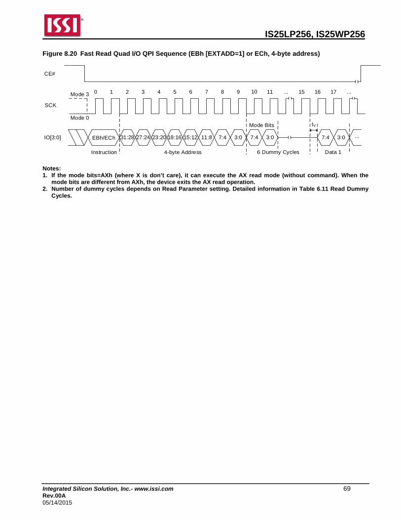
IS25LP256, IS25WP256
Integrated Silicon Solution, Inc.- www.issi.com 69 Rev.00A 05/14/2015
Figure 8.20 Fast Read Quad I/O QPI Sequence (EBh [EXTADD=1] or ECh, 4-byte address)
EBh/ECh
CE#
IO[3:0]
6 Dummy Cycles4-byte Address
0 1 2 3 4 5 6 7 8 9
...
11 ... 15 16 17Mode 3
Mode 0
31:28 7:4 3:07:4 3:0
Data 1
27:24 23:20 18:16 15:12 11:8
...
tV
Instruction
Mode Bits
7:4 3:0
10
SCK
Notes: 1. If the mode bits=AXh (where X is don’t care), it can execute the AX read mode (without command). When the
mode bits are different from AXh, the device exits the AX read operation. 2. Number of dummy cycles depends on Read Parameter setting. Detailed information in Table 6.11 Read Dummy
Cycles.
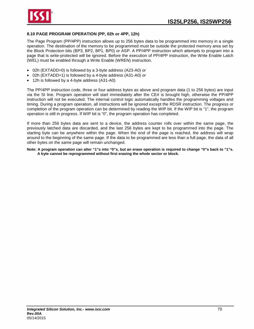
IS25LP256, IS25WP256
Integrated Silicon Solution, Inc.- www.issi.com 70 Rev.00A 05/14/2015
8.10 PAGE PROGRAM OPERATION (PP, 02h or 4PP, 12h)
The Page Program (PP/4PP) instruction allows up to 256 bytes data to be programmed into memory in a single operation. The destination of the memory to be programmed must be outside the protected memory area set by the Block Protection bits (BP3, BP2, BP1, BP0) or ASP. A PP/4PP instruction which attempts to program into a page that is write-protected will be ignored. Before the execution of PP/4PP instruction, the Write Enable Latch (WEL) must be enabled through a Write Enable (WREN) instruction. • 02h (EXTADD=0) is followed by a 3-byte address (A23-A0) or • 02h (EXTADD=1) is followed by a 4-byte address (A31-A0) or • 12h is followed by a 4-byte address (A31-A0) The PP/4PP instruction code, three or four address bytes as above and program data (1 to 256 bytes) are input via the SI line. Program operation will start immediately after the CE# is brought high, otherwise the PP/4PP instruction will not be executed. The internal control logic automatically handles the programming voltages and timing. During a program operation, all instructions will be ignored except the RDSR instruction. The progress or completion of the program operation can be determined by reading the WIP bit. If the WIP bit is “1”, the program operation is still in progress. If WIP bit is “0”, the program operation has completed. If more than 256 bytes data are sent to a device, the address counter rolls over within the same page, the previously latched data are discarded, and the last 256 bytes are kept to be programmed into the page. The starting byte can be anywhere within the page. When the end of the page is reached, the address will wrap around to the beginning of the same page. If the data to be programmed are less than a full page, the data of all other bytes on the same page will remain unchanged.
Note: A program operation can alter “1”s into “0”s, but an erase operation is required to change “0”s back to “1”s. A byte cannot be reprogrammed without first erasing the whole sector or block.
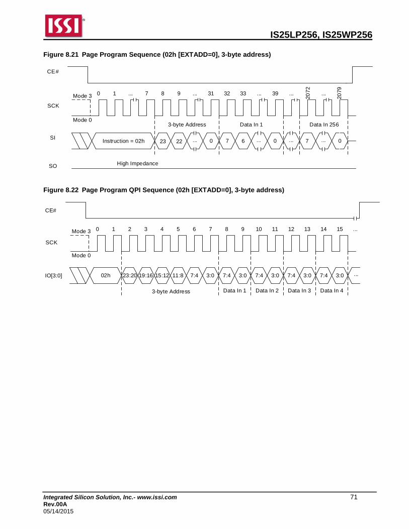
IS25LP256, IS25WP256
Integrated Silicon Solution, Inc.- www.issi.com 71 Rev.00A 05/14/2015
Figure 8.21 Page Program Sequence (02h [EXTADD=0], 3-byte address)
Instruction = 02h 23
CE#
SCK
SI 7 6
SO
7
3-byte Address
High Impedance
22 ... 0
Data In 1 Data In 256
0 1 ... 7 8 9 ... 31 32 33 ... 39 ...
2072 ...
2079
Mode 3
Mode 0
... 0 ... ... 0
Figure 8.22 Page Program QPI Sequence (02h [EXTADD=0], 3-byte address)
02h
CE#
SCK
IO[3:0]
3-byte Address
0 1 2 3 4 5 6 7 8 9 10 11 12 13 14 15Mode 3
Mode 0
23:20 7:4 3:0 7:4 3:0
Data In 1 Data In 2
19:16 15:12 11:8 7:4 3:0 7:4 3:0 7:4 3:0
Data In 3 Data In 4
...
...

IS25LP256, IS25WP256
Integrated Silicon Solution, Inc.- www.issi.com 72 Rev.00A 05/14/2015
Figure 8.23 Page Program Sequence (02h [EXTADD=1] or 12h, 4-byte address)
Instruction = 02h/12h 31
CE#
SCK
SI 7 6
SO
7
4-byte Address
High Impedance
30 ... 0
Data In 1 Data In 256
0 1 ... 7 8 9 ... 39 40 41 ... 47 ...
2080 ...
2087
Mode 3
Mode 0
... 0 ... ... 0
Figure 8.24 Page Program QPI Sequence (02h [EXTADD=1] or 12h, 4-byte address)
02h/12h
CE#
SCK
IO[3:0]
4-byte Address
0 1 2 3 4 5 6 7 8 9 10 11 12 13 14 15Mode 3
Mode 0
31:28 7:4 3:0 7:4 3:0
Data In 1
27:24 23:20 19:16 15:12 11:8 7:4 3:0 7:4 3:0
Data In 2 Data In 3
...
...

IS25LP256, IS25WP256
Integrated Silicon Solution, Inc.- www.issi.com 73 Rev.00A 05/14/2015
8.11 QUAD INPUT PAGE PROGRAM OPERATION (PPQ, 32h/38h or 4PPQ, 34h/3Eh)
The Quad Input Page Program instruction allows up to 256 bytes data to be programmed into memory in a single operation with four pins (IO0, IO1, IO2 and IO3). The destination of the memory to be programmed must be outside the protected memory area set by the Block Protection (BP3, BP2, BP1, BP0) bits or ASP. A Quad Input Page Program instruction which attempts to program into a page that is write-protected will be ignored. Before the execution of Quad Input Page Program instruction, the QE bit in the Status Register must be set to “1” and the Write Enable Latch (WEL) must be enabled through a Write Enable (WREN) instruction. • 32h/38h (EXTADD=0) is followed by a 3-byte address (A23-A0) or • 32h/38h (EXTADD=1) is followed by a 4-byte address (A31-A0) or • 34h/3Eh is followed by a 4-byte address (A31-A0) The Quad Input Page Program instruction code, three or four address bytes as above and program data (1 to 256 bytes) are input via the four pins (IO0, IO1, IO2 and IO3). Program operation will start immediately after the CE# is brought high, otherwise the Quad Input Page Program instruction will not be executed. The internal control logic automatically handles the programming voltages and timing. During a program operation, all instructions will be ignored except the RDSR instruction. The progress or completion of the program operation can be determined by reading the WIP bit. If the WIP bit is “1”, the program operation is still in progress. If WIP bit is “0”, the program operation has completed. If more than 256 bytes data are sent to a device, the address counter rolls over within the same page, the previously latched data are discarded, and the last 256 bytes data are kept to be programmed into the page. The starting byte can be anywhere within the page. When the end of the page is reached, the address will wrap around to the beginning of the same page. If the data to be programmed are less than a full page, the data of all other bytes on the same page will remain unchanged.
Note: A program operation can alter “1”s into “0”s, but an erase operation is required to change “0”s back to “1”s. A byte cannot be reprogrammed without first erasing the whole sector or block.
Figure 8.25 Quad Input Page Program operation (32h/38h [EXTADD=0], 3-byte address)
Instruction = 32h/38h 23
CE#
SCK
4 0 4 0
3-byte Address
High Impedance
22 ... 0
0 1 2 3 4 5 6 7 8 9 31 32 33 34 35Mode 3
Mode 0
IO0
IO1 5 1 5 1
6 2 6 2
7 3 7 3
Data In 2
IO2
IO3
...
Data In 1
...
...
...
...
...
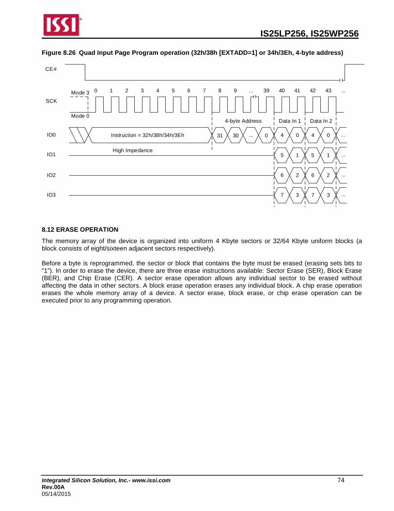
IS25LP256, IS25WP256
Integrated Silicon Solution, Inc.- www.issi.com 74 Rev.00A 05/14/2015
Figure 8.26 Quad Input Page Program operation (32h/38h [EXTADD=1] or 34h/3Eh, 4-byte address)
31
4-byte Address
30
39 40 41 42 43
Instruction = 32h/38h/34h/3Eh
CE#
SCK
4 0 4 0
High Impedance
... 0
0 1 2 3 4 5 6 7 8 9Mode 3
Mode 0
IO0
IO1 5 1 5 1
6 2 6 2
7 3 7 3
Data In 2
IO2
IO3
...
Data In 1
...
...
...
...
...
8.12 ERASE OPERATION
The memory array of the device is organized into uniform 4 Kbyte sectors or 32/64 Kbyte uniform blocks (a block consists of eight/sixteen adjacent sectors respectively). Before a byte is reprogrammed, the sector or block that contains the byte must be erased (erasing sets bits to “1”). In order to erase the device, there are three erase instructions available: Sector Erase (SER), Block Erase (BER), and Chip Erase (CER). A sector erase operation allows any individual sector to be erased without affecting the data in other sectors. A block erase operation erases any individual block. A chip erase operation erases the whole memory array of a device. A sector erase, block erase, or chip erase operation can be executed prior to any programming operation.

IS25LP256, IS25WP256
Integrated Silicon Solution, Inc.- www.issi.com 75 Rev.00A 05/14/2015
8.13 SECTOR ERASE OPERATION (SER, D7h/20h or 4SER, 21h)
A Sector Erase (SER/4SER) instruction erases a 4 Kbyte sector before the execution of a SER/4SER instruction, the Write Enable Latch (WEL) must be set via a Write Enable (WREN) instruction. The WEL bit is automatically reset after the completion of Sector Erase operation. • D7h/20h (EXTADD=0) is followed by a 3-byte address (A23-A0) or • D7h/20h (EXTADD=1) is followed by a 4-byte address (A31-A0) or • 21h is followed by a 4-byte address (A31-A0) A SER/4SER instruction is entered, after CE# is pulled low to select the device and stays low during the entire instruction sequence The SER/4SER instruction code, and three or four address bytes as above are input via SI. Erase operation will start immediately after CE# is pulled high. The internal control logic automatically handles the erase voltage and timing. During an erase operation, all instruction will be ignored except Read Status Register, Read Extended Read Register, Erase/Program Suspend, and Software/Hardware Reset instructions. The progress or completion of the erase operation can be determined by reading the WIP bit. If the WIP bit is “1”, the erase operation is still in progress. If the WIP bit is “0”, the erase operation has been completed. Figure 8.27 Sector Erase Sequence (D7h/20h [EXTADD=0], 3-byte address)
Instruction = D7h/20h 23
CE#
SCK
SI 3 2
SO
1 0
3-byte Address
High Impedance
22 21 ...
0 1 2 3 4 5 6 7 8 9 10 ... 28 29 30 31Mode 3
Mode 0
IS25LP256, IS25WP256
Integrated Silicon Solution, Inc.- www.issi.com 76 Rev.00A 05/14/2015
Figure 8.28 Sector Erase Sequence (D7h/20h [EXTADD=1] or 21h, 4-byte address)
31 30 29
36 37 38 39
Instruction = D7h/20h/21h
CE#
SCK
SI 3 2
SO
1 0
4-byte Address
High Impedance
...
0 1 2 3 4 5 6 7 8 9 10 ...Mode 3
Mode 0
Figure 8.29 Sector Erase QPI Sequence (D7h/20h [EXTADD=0], 3-byte address)
D7h/20h
CE#
SCK
IO[3:0]
3-byte Address
0 1 2 3 4 5 6 7Mode 3
Mode 0
23:20 19:16 15:12 11:8 7:4 3:0
Figure 8.30 Sector Erase QPI Sequence (D7h/20h [EXTADD=1] or 21h, 4-byte address)
CE#
4-byte Address
23:20 19:16 15:12 11:8 7:4 3:031:28 27:24
8 9
D7h/20h/21h
SCK
IO[3:0]
0 1 2 3 4 5 6 7Mode 3
Mode 0
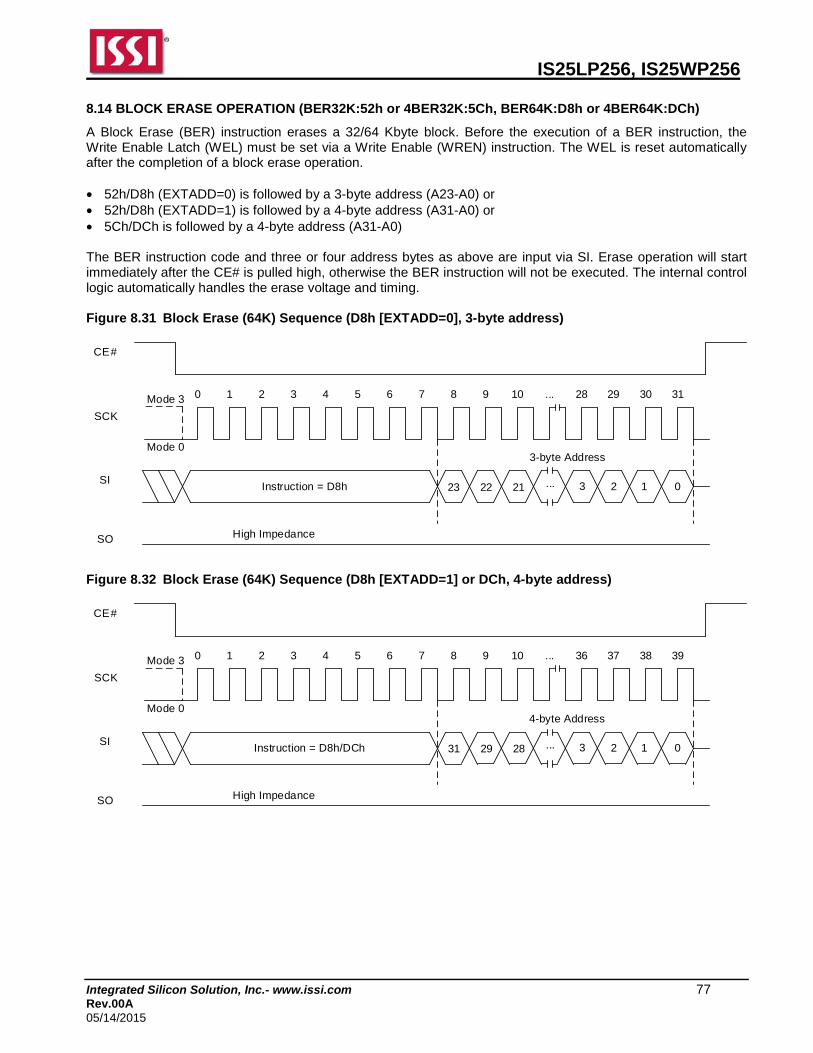
IS25LP256, IS25WP256
Integrated Silicon Solution, Inc.- www.issi.com 77 Rev.00A 05/14/2015
8.14 BLOCK ERASE OPERATION (BER32K:52h or 4BER32K:5Ch, BER64K:D8h or 4BER64K:DCh)
A Block Erase (BER) instruction erases a 32/64 Kbyte block. Before the execution of a BER instruction, the Write Enable Latch (WEL) must be set via a Write Enable (WREN) instruction. The WEL is reset automatically after the completion of a block erase operation. • 52h/D8h (EXTADD=0) is followed by a 3-byte address (A23-A0) or • 52h/D8h (EXTADD=1) is followed by a 4-byte address (A31-A0) or • 5Ch/DCh is followed by a 4-byte address (A31-A0) The BER instruction code and three or four address bytes as above are input via SI. Erase operation will start immediately after the CE# is pulled high, otherwise the BER instruction will not be executed. The internal control logic automatically handles the erase voltage and timing. Figure 8.31 Block Erase (64K) Sequence (D8h [EXTADD=0], 3-byte address)
Instruction = D8h 23
CE#
SCK
SI 3 2
SO
1 0
3-byte Address
High Impedance
22 21 ...
0 1 2 3 4 5 6 7 8 9 10 ... 28 29 30 31Mode 3
Mode 0
Figure 8.32 Block Erase (64K) Sequence (D8h [EXTADD=1] or DCh, 4-byte address)
31
4-byte Address
29 28
36 37 38 39
Instruction = D8h/DCh
CE#
SCK
SI 3 2
SO
1 0
High Impedance
...
0 1 2 3 4 5 6 7 8 9 10 ...Mode 3
Mode 0
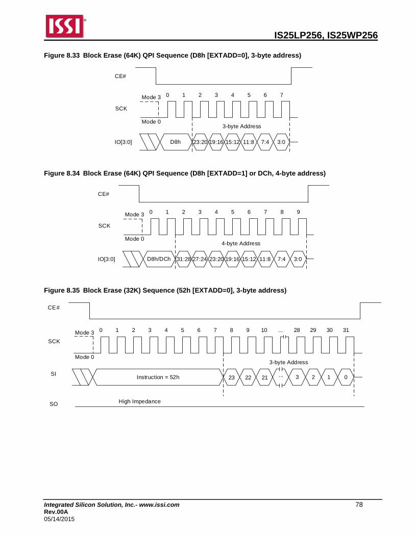
IS25LP256, IS25WP256
Integrated Silicon Solution, Inc.- www.issi.com 78 Rev.00A 05/14/2015
Figure 8.33 Block Erase (64K) QPI Sequence (D8h [EXTADD=0], 3-byte address)
D8h
CE#
SCK
IO[3:0]
3-byte Address
0 1 2 3 4 5 6 7Mode 3
Mode 0
23:20 19:16 15:12 11:8 7:4 3:0
Figure 8.34 Block Erase (64K) QPI Sequence (D8h [EXTADD=1] or DCh, 4-byte address)
D8h/DCh
CE#
SCK
IO[3:0]
4-byte Address
0 1 2 3 4 5 6 7Mode 3
Mode 0
23:20 19:16 15:12 11:8 7:4 3:031:28 27:24
8 9
Figure 8.35 Block Erase (32K) Sequence (52h [EXTADD=0], 3-byte address)
Instruction = 52h 23
CE#
SCK
SI 3 2
SO
1 0
3-byte Address
High Impedance
22 21 ...
0 1 2 3 4 5 6 7 8 9 10 ... 28 29 30 31Mode 3
Mode 0
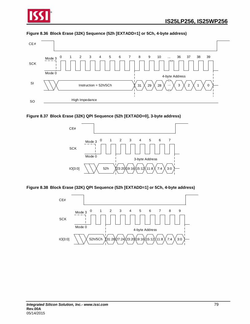
IS25LP256, IS25WP256
Integrated Silicon Solution, Inc.- www.issi.com 79 Rev.00A 05/14/2015
Figure 8.36 Block Erase (32K) Sequence (52h [EXTADD=1] or 5Ch, 4-byte address)
Instruction = 52h/5Ch 31
CE#
SCK
SI 3 2
SO
1 0
4-byte Address
High Impedance
29 28 ...
0 1 2 3 4 5 6 7 8 9 10 ... 36 37 38 39Mode 3
Mode 0
Figure 8.37 Block Erase (32K) QPI Sequence (52h [EXTADD=0], 3-byte address)
52h
CE#
SCK
IO[3:0]
3-byte Address
0 1 2 3 4 5 6 7Mode 3
Mode 0
23:20 19:16 15:12 11:8 7:4 3:0
Figure 8.38 Block Erase (32K) QPI Sequence (52h [EXTADD=1] or 5Ch, 4-byte address)
52h/5Ch
CE#
SCK
IO[3:0]
4-byte Address
0 1 2 3 4 5 6 7Mode 3
Mode 0
23:20 19:16 15:12 11:8 7:4 3:031:28 27:24
8 9
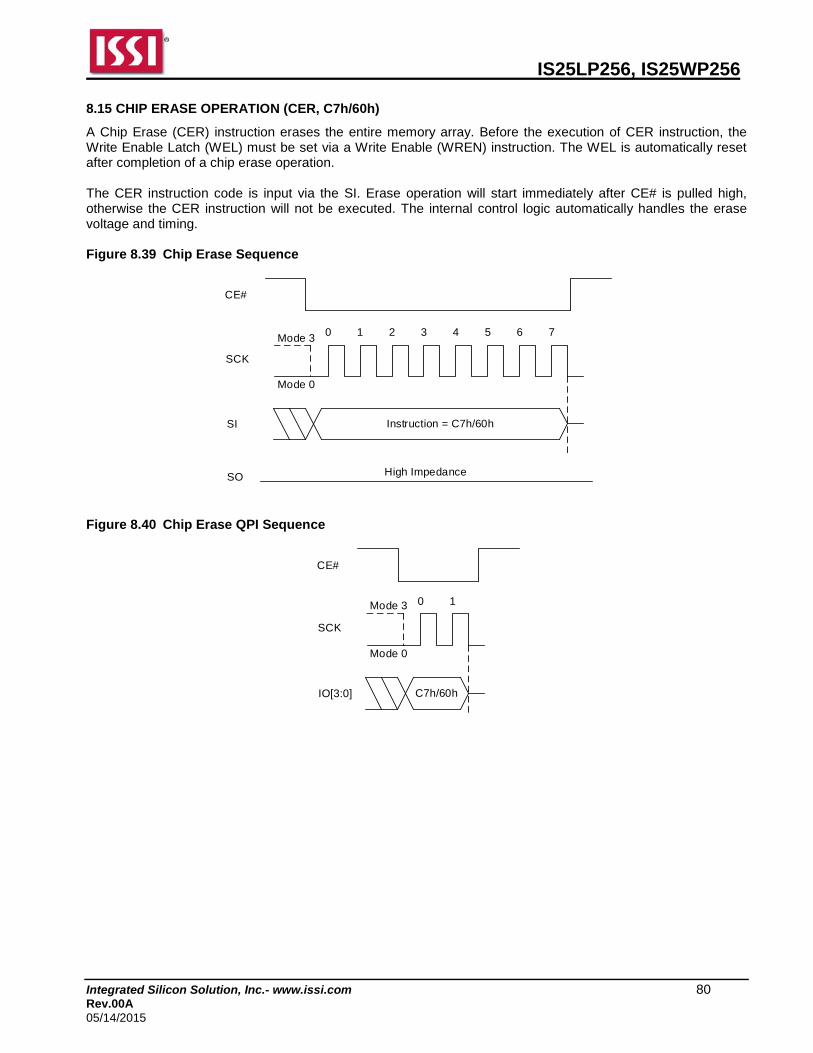
IS25LP256, IS25WP256
Integrated Silicon Solution, Inc.- www.issi.com 80 Rev.00A 05/14/2015
8.15 CHIP ERASE OPERATION (CER, C7h/60h)
A Chip Erase (CER) instruction erases the entire memory array. Before the execution of CER instruction, the Write Enable Latch (WEL) must be set via a Write Enable (WREN) instruction. The WEL is automatically reset after completion of a chip erase operation. The CER instruction code is input via the SI. Erase operation will start immediately after CE# is pulled high, otherwise the CER instruction will not be executed. The internal control logic automatically handles the erase voltage and timing. Figure 8.39 Chip Erase Sequence
Instruction = C7h/60h
CE#
SCK
SI
0 1 2 3 4 5 6 7Mode 3
Mode 0
SO High Impedance
Figure 8.40 Chip Erase QPI Sequence
C7h/60h
CE#
SCK
IO[3:0]
0 1Mode 3
Mode 0
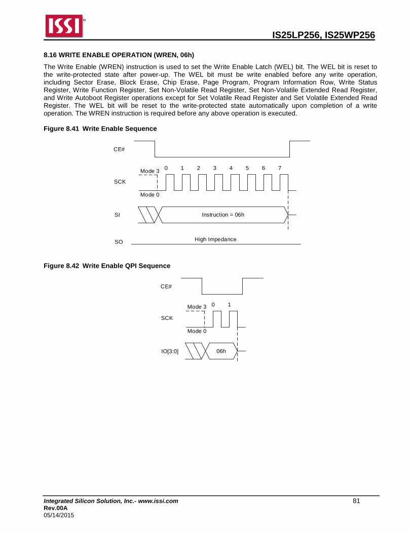
IS25LP256, IS25WP256
Integrated Silicon Solution, Inc.- www.issi.com 81 Rev.00A 05/14/2015
8.16 WRITE ENABLE OPERATION (WREN, 06h)
The Write Enable (WREN) instruction is used to set the Write Enable Latch (WEL) bit. The WEL bit is reset to the write-protected state after power-up. The WEL bit must be write enabled before any write operation, including Sector Erase, Block Erase, Chip Erase, Page Program, Program Information Row, Write Status Register, Write Function Register, Set Non-Volatile Read Register, Set Non-Volatile Extended Read Register, and Write Autoboot Register operations except for Set Volatile Read Register and Set Volatile Extended Read Register. The WEL bit will be reset to the write-protected state automatically upon completion of a write operation. The WREN instruction is required before any above operation is executed. Figure 8.41 Write Enable Sequence
Instruction = 06h
CE#
SCK
SI
0 1 2 3 4 5 6 7Mode 3
Mode 0
SO High Impedance
Figure 8.42 Write Enable QPI Sequence
06h
CE#
SCK
IO[3:0]
0 1Mode 3
Mode 0

IS25LP256, IS25WP256
Integrated Silicon Solution, Inc.- www.issi.com 82 Rev.00A 05/14/2015
8.17 WRITE DISABLE OPERATION (WRDI, 04h)
The Write Disable (WRDI) instruction resets the WEL bit and disables all write instructions. The WRDI instruction is not required after the execution of a write instruction, since the WEL bit is automatically reset. Figure 8.43 Write Disable Sequence
Instruction = 04h
CE#
SCK
SI
0 1 2 3 4 5 6 7Mode 3
Mode 0
SO High Impedance
Figure 8.44 Write Disable QPI Sequence
04h
CE#
SCK
IO[3:0]
0 1Mode 3
Mode 0
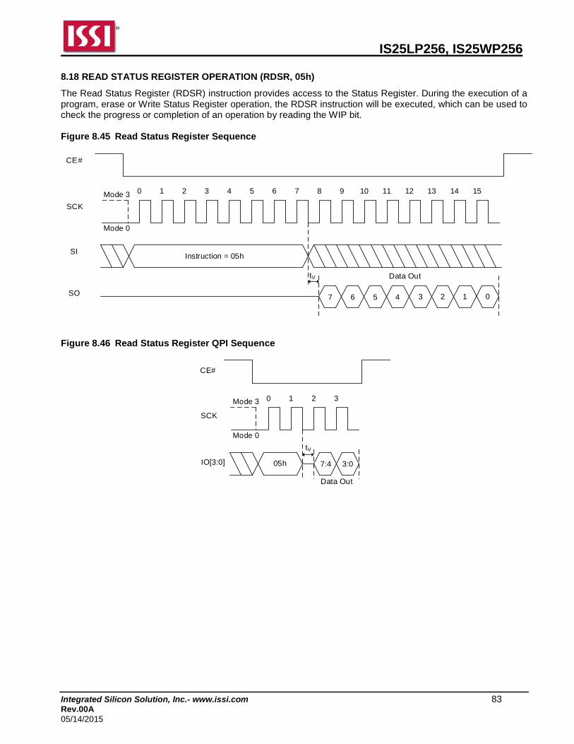
IS25LP256, IS25WP256
Integrated Silicon Solution, Inc.- www.issi.com 83 Rev.00A 05/14/2015
8.18 READ STATUS REGISTER OPERATION (RDSR, 05h)
The Read Status Register (RDSR) instruction provides access to the Status Register. During the execution of a program, erase or Write Status Register operation, the RDSR instruction will be executed, which can be used to check the progress or completion of an operation by reading the WIP bit. Figure 8.45 Read Status Register Sequence
Instruction = 05h
7
CE#
SCK
SI
3 2SO 1 0
Data Out
6 5
0 1 2 3 4 5 6 7 8 9 10 11 12 13 14 15Mode 3
Mode 0
4
tV
Figure 8.46 Read Status Register QPI Sequence
05h
0 1Mode 3
Mode 0
2 3
7:4 3:0
CE#
SCK
IO[3:0]
tV
Data Out
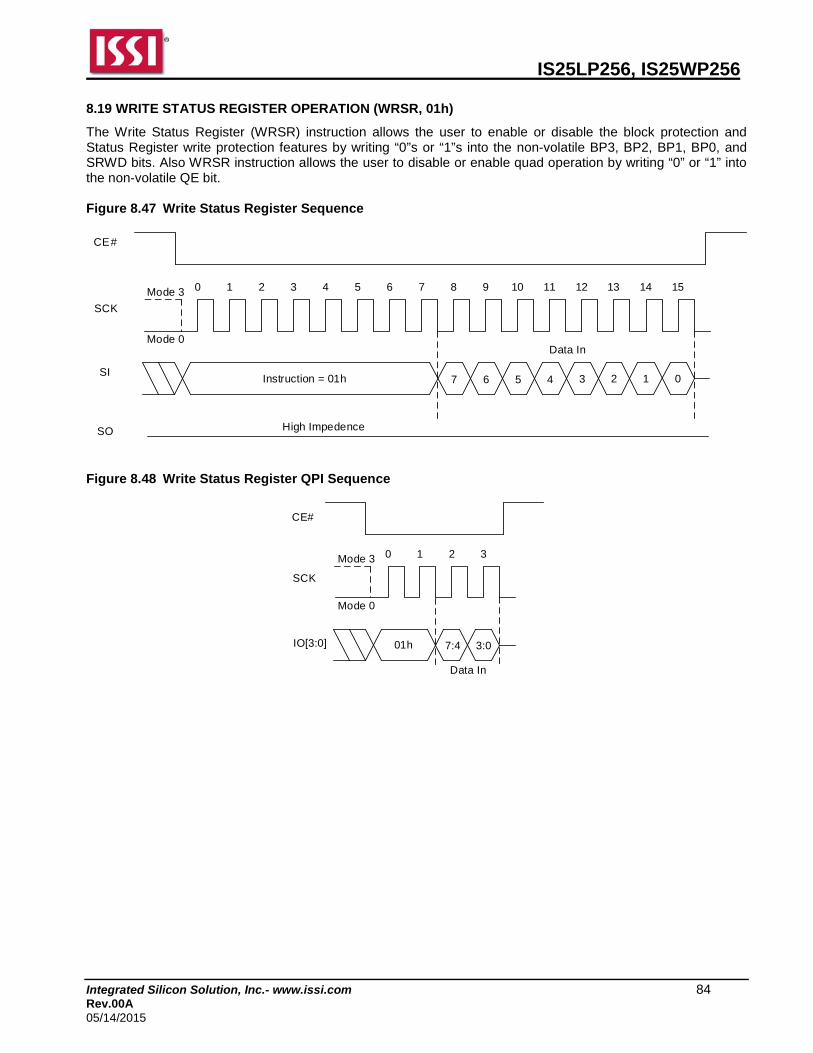
IS25LP256, IS25WP256
Integrated Silicon Solution, Inc.- www.issi.com 84 Rev.00A 05/14/2015
8.19 WRITE STATUS REGISTER OPERATION (WRSR, 01h)
The Write Status Register (WRSR) instruction allows the user to enable or disable the block protection and Status Register write protection features by writing “0”s or “1”s into the non-volatile BP3, BP2, BP1, BP0, and SRWD bits. Also WRSR instruction allows the user to disable or enable quad operation by writing “0” or “1” into the non-volatile QE bit. Figure 8.47 Write Status Register Sequence
Instruction = 01h
CE#
SCK
SI
SO
Data In
0 1 2 3 4 5 6 7 8 9 10 11 12 13 14 15Mode 3
Mode 0
7 3 2 1 06 5 4
High Impedence
Figure 8.48 Write Status Register QPI Sequence
01h
0 1Mode 3
Mode 0
2 3
7:4 3:0
CE#
SCK
IO[3:0]
Data In

IS25LP256, IS25WP256
Integrated Silicon Solution, Inc.- www.issi.com 85 Rev.00A 05/14/2015
8.20 READ FUNCTION REGISTER OPERATION (RDFR, 48h)
The Read Function Register (RDFR) instruction provides access to the Function Register. Refer to Table 6.6 Function Register Bit Definition for more detail. Figure 8.49 Read Function Register Sequence
Instruction = 48h
7
CE#
SCK
SI
3 2SO 1 0
Data Out
6 5
0 1 2 3 4 5 6 7 8 9 10 11 12 13 14 15Mode 3
Mode 0
4
tV
Figure 8.50 Read Function Register QPI Sequence
48h
0 1Mode 3
Mode 0
2 3
7:4 3:0
CE#
SCK
IO[3:0]
tV
Data Out
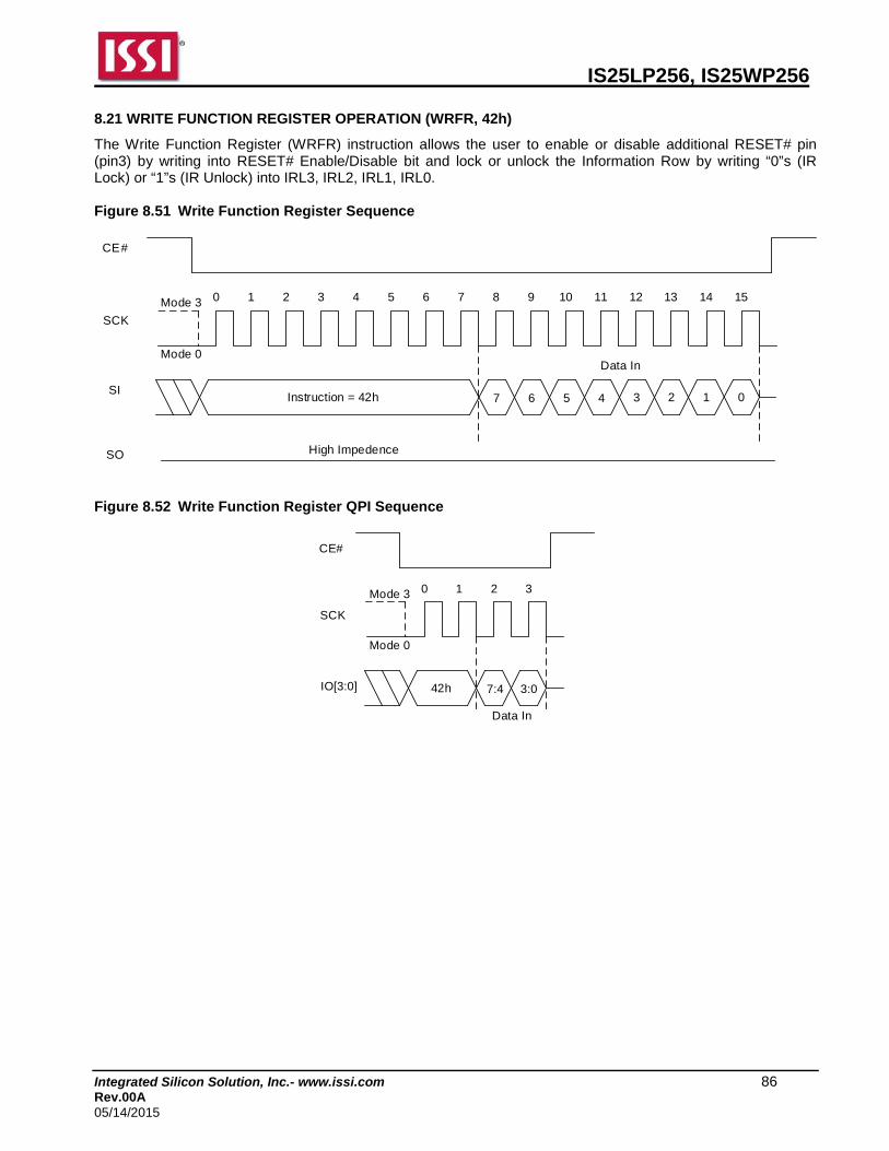
IS25LP256, IS25WP256
Integrated Silicon Solution, Inc.- www.issi.com 86 Rev.00A 05/14/2015
8.21 WRITE FUNCTION REGISTER OPERATION (WRFR, 42h)
The Write Function Register (WRFR) instruction allows the user to enable or disable additional RESET# pin (pin3) by writing into RESET# Enable/Disable bit and lock or unlock the Information Row by writing “0”s (IR Lock) or “1”s (IR Unlock) into IRL3, IRL2, IRL1, IRL0. Figure 8.51 Write Function Register Sequence
Instruction = 42h
CE#
SCK
SI
SO
Data In
0 1 2 3 4 5 6 7 8 9 10 11 12 13 14 15Mode 3
Mode 0
7 3 2 1 06 5 4
High Impedence
Figure 8.52 Write Function Register QPI Sequence
42h
0 1Mode 3
Mode 0
2 3
7:4 3:0
CE#
SCK
IO[3:0]
Data In

IS25LP256, IS25WP256
Integrated Silicon Solution, Inc.- www.issi.com 87 Rev.00A 05/14/2015
8.22 ENTER QUAD PERIPHERAL INTERFACE (QPI) MODE OPERATION (QIOEN,35h; QIODI,F5h)
The Enter Quad I/O (QIOEN) instruction, 35h, enables the Flash device for QPI bus operation. Upon completion of the instruction, all instructions thereafter will be 4-bit multiplexed input/output until a power cycle or an Exit Quad I/O instruction is sent to device. The Exit Quad I/O instruction, F5h, resets the device to 1-bit SPI protocol operation. To execute an Exit Quad I/O operation, the host drives CE# low, sends the Exit Quad I/O command cycle, then drives CE# high. The device just accepts QPI (2 clocks) command cycles. Figure 8.53 Enter Quad Peripheral Interface (QPI) Mode Sequence
Instruction = 35h
CE#
SCK
SI
0 1 2 3 4 5 6 7Mode 3
Mode 0
SO High Impedance
Figure 8.54 Exit Quad Peripheral Interface (QPI) Mode Sequence
F5h
CE#
SCK
IO[3:0]
0 1Mode 3
Mode 0

IS25LP256, IS25WP256
Integrated Silicon Solution, Inc.- www.issi.com 88 Rev.00A 05/14/2015
8.23 PROGRAM/ERASE SUSPEND & RESUME
The device allows the interruption of Sector Erase, Block Erase, or Page Program operations to conduct other operations. 75h/B0h/85h command for suspend and 7Ah/30h/8Ah for resume will be used. (SPI/QPI all acceptable) Function Register bit2 (PSUS) and bit3 (ESUS) are used to check whether or not the device is in suspend mode. Suspend to read ready timing: 100µs Resume to another suspend timing: 400µs PROGRAM/ERASE SUSPEND DURING SECTOR-ERASE OR BLOCK-ERASE (PERSUS 75h/B0h/85h) The Program/Erase Suspend allows the interruption of Sector Erase and Block Erase operations. After the Program/Erase Suspend, program, read related, resume and reset commands can be accepted. It is possible to nest a Program/Erase Suspend operation during a Program inside a Program/Erase Suspend operation. Refer to Table 8.7 for more detail. To execute the Program/Erase Suspend operation, the host drives CE# low, sends the Program/Erase Suspend command cycle (75h/B0h/85h), then drives CE# high. The Function Register indicates that the Erase has been suspended by changing the ESUS bit from “0” to “1”, but the device will not accept another command until it is ready. To determine when the device will accept a new command, poll the WIP bit or wait the specified time tSUS. When ESUS bit is issued, the Write Enable Latch (WEL) bit will be reset. PROGRAM/ERASE SUSPEND DURING PAGE PROGRAMMING (PERSUS 75h/B0h/85h) The Program/Erase Suspend allows the interruption of an array Program operation. After the Program/Erase Suspend command, WEL bit will be disabled, therefore only read related, resume and reset commands can be accepted. Refer to Table 8.7 for more detail. To execute the Program/Erase Suspend operation, the host drives CE# low, sends the Program/Erase Suspend command cycle (75h/B0h/85h), then drives CE# high. The Function Register indicates that the programming has been suspended by changing the PSUS bit from “0” to “1”, but the device will not accept another command until it is ready. To determine when the device will accept a new command, poll the WIP bit or wait the specified time tSUS. PROGRAM/ERASE RESUME (PERRSM 7Ah/30h/8Ah) The Program/Erase Resume restarts the Program or Erase command that was suspended, and changes the suspend status bit in the Function Register (ESUS or PSUS bits) back to “0”. To execute the Program/Erase Resume operation, the host drives CE# low, sends the Program/Erase Resume command cycle (7Ah/30h/8Ah), then drives CE# high. A cycle is two nibbles long, most significant nibble first. To determine if the internal, self-timed Write operation completed, poll the WIP bit, or wait the specified time tSE, tBE or tPP for Sector Erase, Block Erase, or Page Programming, respectively. The total write time before suspend and after resume will not exceed the uninterrupted write times tSE, tBE or tPP.

IS25LP256, IS25WP256
Integrated Silicon Solution, Inc.- www.issi.com 89 Rev.00A 05/14/2015
Table 8.7 Instructions accepted during Suspend
Operation Suspended
Instruction Allowed
Name Hex Code Operation
Program or Erase NORD 03h Normal Read Mode
Program or Erase 4NORD 13h 4-byte Address Normal Read Mode
Program or Erase FRD 0Bh Fast Read Mode
Program or Erase 4FRD 0Ch 4-byte Address Fast Read Mode
Program or Erase FRDIO BBh Fast Read Dual I/O
Program or Erase 4FRDIO BCh 4-byte Address Fast Read Dual I/O
Program or Erase FRDO 3Bh Fast Read Dual Output
Program or Erase 4FRDO 3Ch 4-byte Address Fast Read Dual Output
Program or Erase FRQIO EBh Fast Read Quad I/O
Program or Erase 4FRQIO ECh 4-byte Address Fast Read Quad I/O
Program or Erase FRQO 6Bh Fast Read Quad Output
Program or Erase 4FRQO 6Ch 4-byte Address Fast Read Quad Output
Program or Erase FRDTR 0Dh Fast Read DTR Mode
Program or Erase 4FRDTR 0Eh 4-byte Address Fast Read DTR Mode
Program or Erase FRDDTR BDh Fast Read Dual I/O DTR
Program or Erase 4FRDDTR BEh 4-byte Address Fast Read Dual I/O DTR
Program or Erase FRQDTR EDh Fast Read Quad I/O DTR
Program or Erase 4FRQDTR EEh 4-byte Address Fast Read Quad I/O DTR
Erase PP 02h Serial Input Page Program
Erase 4PP 12h 4-byte Address Serial Input Page Program
Erase PPQ 32h/38h Quad Input Page Program
Erase 4PPQ 34h/3Eh 4-byte Address Quad Input Page Program
Erase WREN 06h Write Enable
Program or Erase RDSR 05h Read Status Register
Program or Erase RDFR 48h Read Function Register
Erase CLERP 82h Clear Extended Read Register
Program or Erase PERRSM 7Ah/30h/8Ah Program/Erase Resume
Erase PERSUS 75h/B0h/85h Program/Erase Suspend
Program or Erase RDID ABh Read Manufacturer and Product ID
Program or Erase SRPV C0/63h Set Read Parameters (Volatile)
Program or Erase SERPV 83h Set Extended Read Parameters (Volatile)
Program or Erase RDRP 61h Read Read Parameters (Volatile)
Program or Erase RDERP 81h Read Extended Read Parameters (Volatile)
Program or Erase RDJDID 9Fh Read Manufacturer and Product ID by JEDEC ID Command
Program or Erase RDMDID 90h Read Manufacturer and Device ID
Program or Erase RDJDIDQ AFh Read JEDEC ID QPI mode
Program or Erase RDUID 4Bh Read Unique ID Number
Program or Erase RDSFDP 5Ah SFDP Read
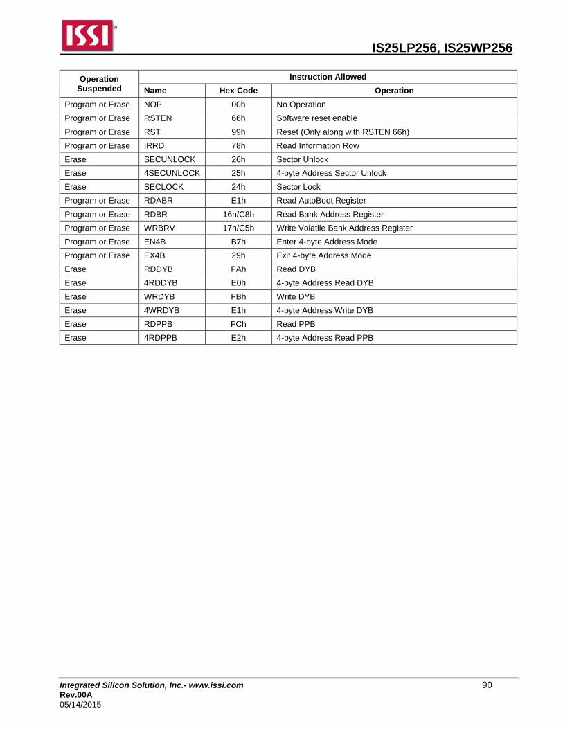
IS25LP256, IS25WP256
Integrated Silicon Solution, Inc.- www.issi.com 90 Rev.00A 05/14/2015
Operation Suspended
Instruction Allowed
Name Hex Code Operation
Program or Erase NOP 00h No Operation
Program or Erase RSTEN 66h Software reset enable
Program or Erase RST 99h Reset (Only along with RSTEN 66h)
Program or Erase IRRD 78h Read Information Row
Erase SECUNLOCK 26h Sector Unlock
Erase 4SECUNLOCK 25h 4-byte Address Sector Unlock
Erase SECLOCK 24h Sector Lock
Program or Erase RDABR E1h Read AutoBoot Register
Program or Erase RDBR 16h/C8h Read Bank Address Register
Program or Erase WRBRV 17h/C5h Write Volatile Bank Address Register
Program or Erase EN4B B7h Enter 4-byte Address Mode
Program or Erase EX4B 29h Exit 4-byte Address Mode
Erase RDDYB FAh Read DYB
Erase 4RDDYB E0h 4-byte Address Read DYB
Erase WRDYB FBh Write DYB
Erase 4WRDYB E1h 4-byte Address Write DYB
Erase RDPPB FCh Read PPB
Erase 4RDPPB E2h 4-byte Address Read PPB
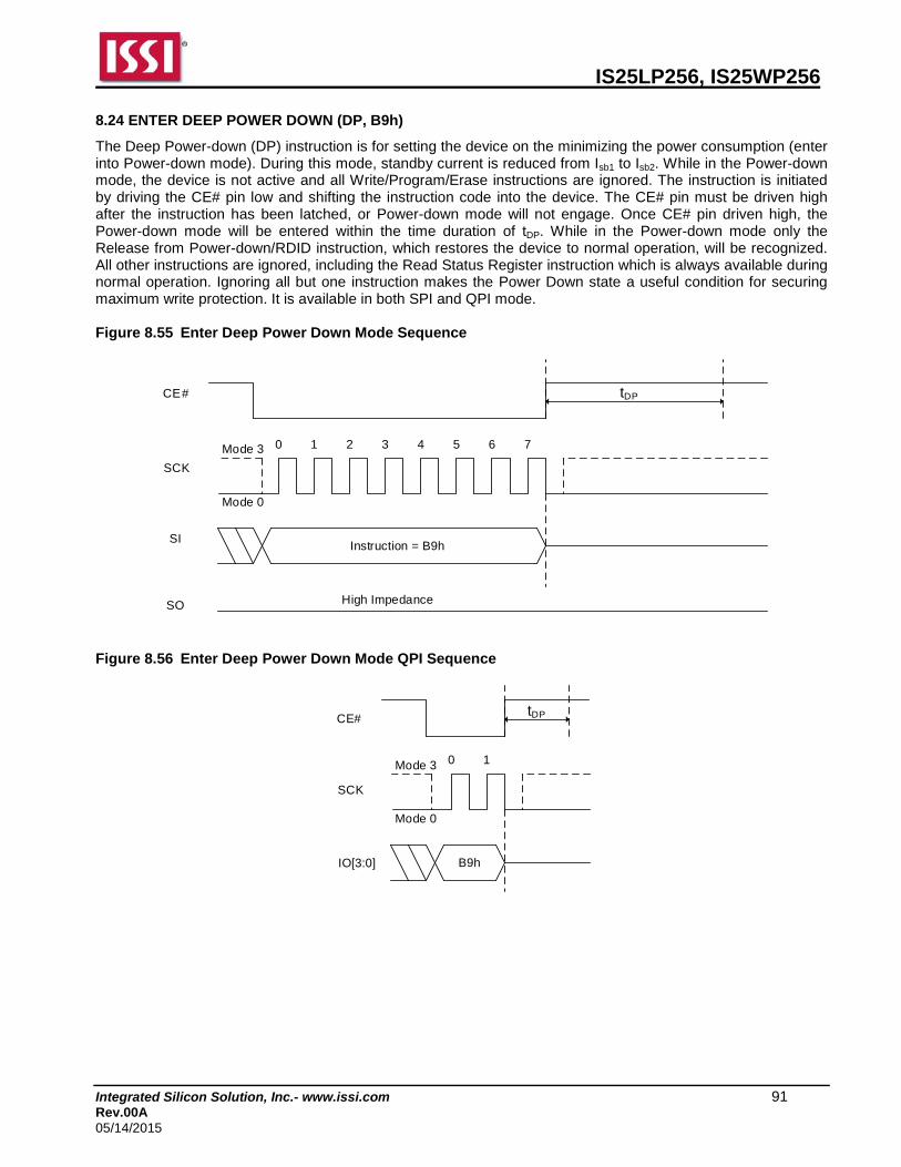
IS25LP256, IS25WP256
Integrated Silicon Solution, Inc.- www.issi.com 91 Rev.00A 05/14/2015
8.24 ENTER DEEP POWER DOWN (DP, B9h)
The Deep Power-down (DP) instruction is for setting the device on the minimizing the power consumption (enter into Power-down mode). During this mode, standby current is reduced from Isb1 to Isb2. While in the Power-down mode, the device is not active and all Write/Program/Erase instructions are ignored. The instruction is initiated by driving the CE# pin low and shifting the instruction code into the device. The CE# pin must be driven high after the instruction has been latched, or Power-down mode will not engage. Once CE# pin driven high, the Power-down mode will be entered within the time duration of tDP. While in the Power-down mode only the Release from Power-down/RDID instruction, which restores the device to normal operation, will be recognized. All other instructions are ignored, including the Read Status Register instruction which is always available during normal operation. Ignoring all but one instruction makes the Power Down state a useful condition for securing maximum write protection. It is available in both SPI and QPI mode. Figure 8.55 Enter Deep Power Down Mode Sequence
Instruction = B9h
CE#
SCK
SI
0 1 2 3 4 5 6 7Mode 3
Mode 0
tDP
SO High Impedance
Figure 8.56 Enter Deep Power Down Mode QPI Sequence
B9h
CE#
SCK
IO[3:0]
0 1Mode 3
Mode 0
tDP

IS25LP256, IS25WP256
Integrated Silicon Solution, Inc.- www.issi.com 92 Rev.00A 05/14/2015
8.25 RELEASE DEEP POWER DOWN (RDPD, ABh)
The Release Deep Power-down/Read Device ID instruction is a multi-purpose command. To release the device from the deep power-down mode, the instruction is issued by driving the CE# pin low, shifting the instruction code into the device and driving CE# high. Releasing the device from Power-down mode will take the time duration of tRES1 before normal operation is restored and other instructions are accepted. The CE# pin must remain high during the tRES1 time duration. If the Release Deep Power-down/RDID instruction is issued while an Erase, Program or Write cycle is in progress (WIP=1) the instruction is ignored and will not have any effects on the current cycle. Figure 8.57 Release Power Down Mode Sequence
tRES1
Instruction = ABh
CE#
SCK
SI
0 1 2 3 4 5 6 7Mode 3
Mode 0
SO High Impedance
Figure 8.58 Release Power Down Mode QPI Sequence
tRES1
ABh
CE#
SCK
IO[3:0]
0 1Mode 3
Mode 0

IS25LP256, IS25WP256
Integrated Silicon Solution, Inc.- www.issi.com 93 Rev.00A 05/14/2015
8.26 SET READ PARAMETERS OPERATION (SRPNV: 65h, SRPV: C0h/63h)
Set Read Parameter Bits This device supports configurable burst length and dummy cycles in both SPI and QPI mode by setting three bits (P2, P1, P0) and four bits (P6, P5, P4, P3) within the Read Register, respectively. To set those bits the SRPNV and SRPV operation instruction are used. Details regarding burst length and dummy cycles can be found in Table 6.9, Table 6.10, and Table 6.11. HOLD#/RESET# pin selection (P7) bit in the Read Register can be set with the SRPNV and SRPV operation as well, in order to select RESET# pin instead of HOLD# pin. For 16-pin SOIC, RESET# pin will be a separate pin and it is independent of the P7 bit setting in Read Register. SRPNV is used to set the non-volatile Read Register, while SRPV is used to set the volatile Read Register.
Note: When SRPNV is executed, the volatile Read Register is set as well as the non-volatile Read Register. Figure 8.59 Set Read Parameters Sequence
Instruction = 65h or C0h/63h
CE#
SCK
SI
SO
Data In
0 1 2 3 4 5 6 7 8 9 10 11 12 13 14 15Mode 3
Mode 0
7 3 2 1 06 5 4
High Impedence
Figure 8.60 Set Read Parameters QPI Sequence
65h or C0h/63h
0 1Mode 3
Mode 0
2 3
7:4 3:0
CE#
SCK
IO[3:0]
Data In

IS25LP256, IS25WP256
Integrated Silicon Solution, Inc.- www.issi.com 94 Rev.00A 05/14/2015
Read with “8/16/32/64-Byte Wrap Around” The device is capable of burst read with wrap around in both SPI and QPI mode. The size of burst length is configurable by using P0, P1, and P2 bits in Read Register. P2 bit (Wrap enable) enables the burst mode feature. P0 and P1 define the size of burst. Burst lengths of 8, 16, 32, and 64 bytes are supported. By default, address increases by one up through the entire array. By setting the burst length, the data being accessed can be limited to the length of burst boundary within a 256 byte page. The first output will be the data at the initial address which is specified in the instruction. Following data will come out from the next address within the burst boundary. Once the address reaches the end of boundary, it will automatically move to the first address of the boundary. CE# high will terminate the command. For example, if burst length of 8 and initial address being applied is 0h, following byte output will be from address 00h and continue to 01h,..,07h, 00h, 01h… until CE# terminates the operation. If burst length of 8 and initial address being applied is FEh(254d), following byte output will be from address FEh and continue to FFh, F8h, F9h, FAh, FBh, FCh, FDh, and repeat from FEh until CE# terminates the operation. The commands, “SRPV (65h) or SRPNV (C0h or 63h)”, are used to configure the burst length. If the following data input is one of “00h”,”01h”,”02h”, and ”03h”, the device will be in default operation mode. It will be continuous burst read of the whole array. If the following data input is one of “04h”,”05h”,”06h”, and ”07h”, the device will set the burst length as 8,16,32 and 64, respectively. To exit the burst mode, another “C0h or 63h” command is necessary to set P2 to 0. Otherwise, the burst mode will be retained until either power down or reset operation. To change burst length, another “C0h or 63h” command should be executed to set P0 and P1 (Detailed information in Table 6.9 Burst Length Data). All read commands will operate in burst mode once the Read Register is set to enable burst mode. Refer to Figure 8.59 and Figure 8.60 for instruction sequence.

IS25LP256, IS25WP256
Integrated Silicon Solution, Inc.- www.issi.com 95 Rev.00A 05/14/2015
8.27 SET EXTENDED READ PARAMETERS OPERATION (SERPNV: 85h, SERPV: 83h)
Set Read Operational Driver Strength This device supports configurable Operational Driver Strength in both SPI and QPI modes by setting three bits (ODS0, ODS1, ODS2) within the Extended Read Register. To set the ODS bits the SERPNV and SERPV operation instructions are required. The device’s driver strength can be reduced as low as 12.50% of full drive strength. Details regarding the driver strength can be found in Table 6.14. SERPNV is used to set the non-volatile Extended Read register, while SERPV is used to set the volatile Extended Read register.
Notes: 1. The default driver strength is set to 50%. 2. When SERPNV is executed, the volatile Read Extended Register is set as well as the non-volatile Read Extended
Register. Figure 8.61 Set Extended Read Parameters Sequence
Instruction = 85h/83h
CE#
SCK
SI
SO
Data In
0 1 2 3 4 5 6 7 8 9 10 11 12 13 14 15Mode 3
Mode 0
7 3 2 1 06 5 4
High Impedence
Figure 8.62 Set Extended Read Parameters QPI Sequence
85h/83h
0 1Mode 3
Mode 0
2 3
7:4 3:0
CE#
SCK
IO[3:0]
Data In
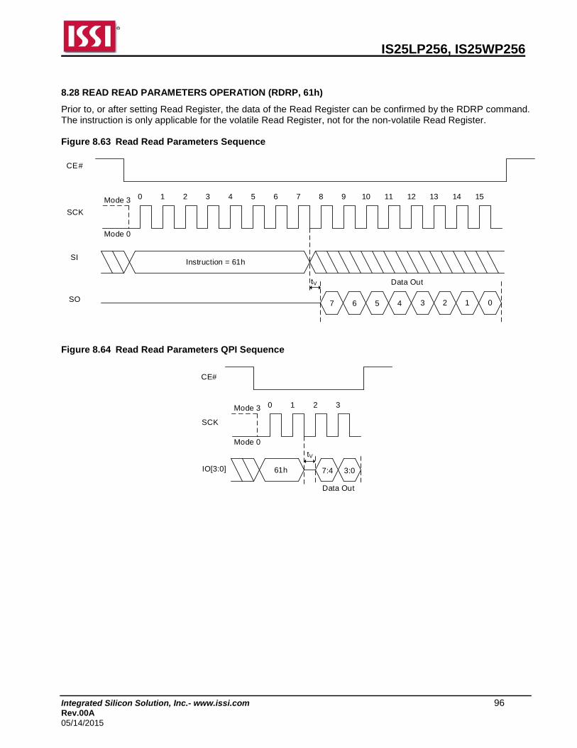
IS25LP256, IS25WP256
Integrated Silicon Solution, Inc.- www.issi.com 96 Rev.00A 05/14/2015
8.28 READ READ PARAMETERS OPERATION (RDRP, 61h)
Prior to, or after setting Read Register, the data of the Read Register can be confirmed by the RDRP command. The instruction is only applicable for the volatile Read Register, not for the non-volatile Read Register. Figure 8.63 Read Read Parameters Sequence
Instruction = 61h
7
CE#
SCK
SI
3 2SO 1 0
Data Out
6 5
0 1 2 3 4 5 6 7 8 9 10 11 12 13 14 15Mode 3
Mode 0
4
tV
Figure 8.64 Read Read Parameters QPI Sequence
61h
0 1Mode 3
Mode 0
2 3
7:4 3:0
CE#
SCK
IO[3:0]
tV
Data Out

IS25LP256, IS25WP256
Integrated Silicon Solution, Inc.- www.issi.com 97 Rev.00A 05/14/2015
8.29 READ EXTENDED READ PARAMETERS OPERATION (RDERP, 81h)
Prior to, or after setting Extended Read Register, the data of the Extended Read Register can be confirmed by the RDERP command. The instruction is only applicable for the volatile Extended Read Register, not for the non-volatile Extended Read Register. During the execution of a program, erase or Write Non-Volatile Register operation, the RDERP instruction will be executed, which can be used to check the progress or completion of an operation by reading the WIP bit. Figure 8.65 Read Extended Read Parameters Sequence
Instruction = 81h
7
CE#
SCK
SI
3 2SO 1 0
Data Out
6 5
0 1 2 3 4 5 6 7 8 9 10 11 12 13 14 15Mode 3
Mode 0
4
tV
Figure 8.66 Read Extended Read Parameters QPI Sequence
81h
0 1Mode 3
Mode 0
2 3
7:4 3:0
CE#
SCK
IO[3:0]
tV
Data Out
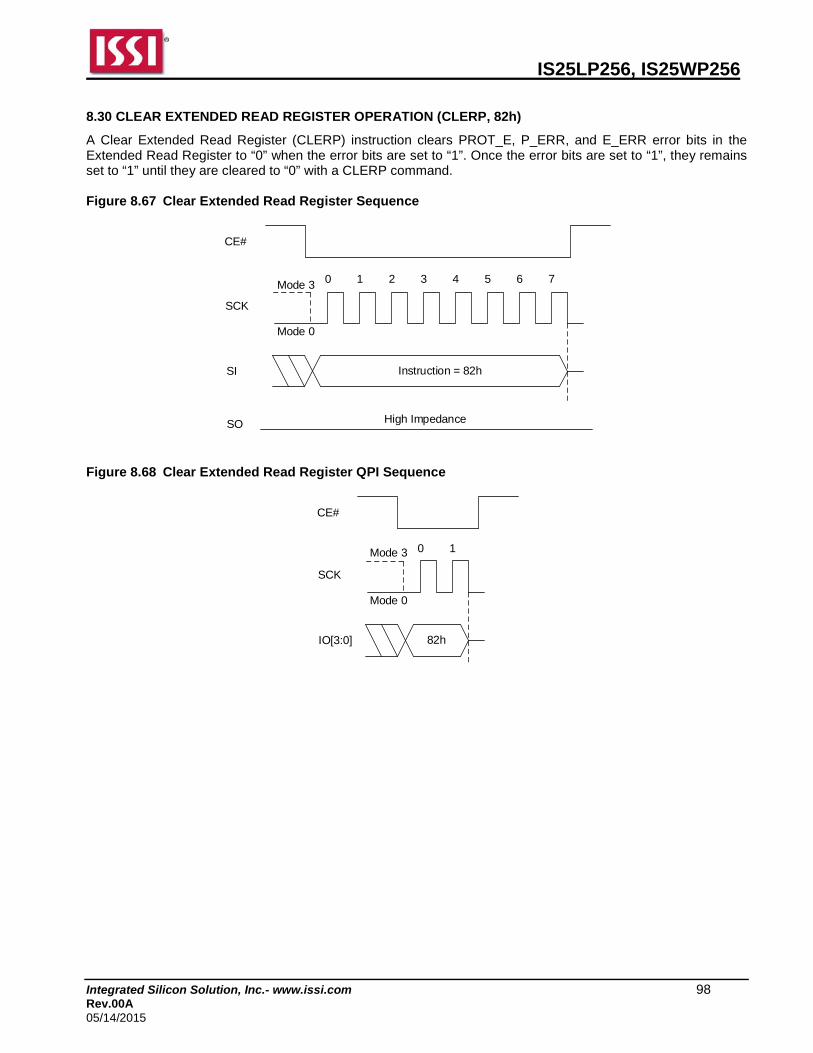
IS25LP256, IS25WP256
Integrated Silicon Solution, Inc.- www.issi.com 98 Rev.00A 05/14/2015
8.30 CLEAR EXTENDED READ REGISTER OPERATION (CLERP, 82h)
A Clear Extended Read Register (CLERP) instruction clears PROT_E, P_ERR, and E_ERR error bits in the Extended Read Register to “0” when the error bits are set to “1”. Once the error bits are set to “1”, they remains set to “1” until they are cleared to “0” with a CLERP command. Figure 8.67 Clear Extended Read Register Sequence
Instruction = 82h
CE#
SCK
SI
0 1 2 3 4 5 6 7Mode 3
Mode 0
SO High Impedance
Figure 8.68 Clear Extended Read Register QPI Sequence
82h
CE#
SCK
IO[3:0]
0 1Mode 3
Mode 0

IS25LP256, IS25WP256
Integrated Silicon Solution, Inc.- www.issi.com 99 Rev.00A 05/14/2015
8.31 READ PRODUCT IDENTIFICATION (RDID, ABh)
The Release from Power-down/Read Device ID instruction is a multi-purpose instruction. It can support both SPI and QPI modes. The Read Product Identification (RDID) instruction is for reading out the old style of 8-bit Electronic Signature, whose values are shown as the table of Product Identification. The RDID instruction code is followed by three dummy bytes, each bit being latched-in on SI during the rising SCK edge. Then the Device ID is shifted out on SO with the MSB first, each bit been shifted out during the falling edge of SCK. The RDID instruction is ended by driving CE# high. The Device ID (ID7-ID0) outputs repeatedly if additional clock cycles are continuously sent to SCK while CE# is at low. Table 8.8 Product Identification
Manufacturer ID (MF7-MF0)
ISSI Serial Flash 9Dh
Instruction ABh 90h 9Fh
Part Number Device ID (ID7-ID0) Memory Type + Capacity (ID15-ID0)
IS25LP256 18h 6019h
IS25WP256 18h 7019h
Figure 8.69 Read Product Identification Sequence
Device ID(ID7-ID0)
Data Out
32 33 ... 39
Instruction = ABh
CE#
SCK
SI
SO
0 1 ... 7 8 9 ... 31Mode 3
Mode 0
3 Dummy Bytes
tV

IS25LP256, IS25WP256
Integrated Silicon Solution, Inc.- www.issi.com 100 Rev.00A 05/14/2015
Figure 8.70 Read Product Identification QPI Sequence
ABh
CE#
SCK
IO[3:0]
0 1Mode 3
Mode 0
2 3 4 5 6 7 8 9
6 Dummy CyclesDevice ID(ID7-ID0)
tV

IS25LP256, IS25WP256
Integrated Silicon Solution, Inc.- www.issi.com 101 Rev.00A 05/14/2015
8.32 READ PRODUCT IDENTIFICATION BY JEDEC ID OPERATION (RDJDID, 9Fh; RDJDIDQ, AFh)
The JEDEC ID READ instruction allows the user to read the manufacturer and product ID of devices. Refer to Table 8.8 Product Identification for Manufacturer ID and Device ID. After the JEDEC ID READ command (9Fh in SPI mode, AFh in QPI mode) is input, the Manufacturer ID is shifted out MSB first followed by the 2-byte electronic ID (ID15-ID0) that indicates Memory Type and Capacity, one bit at a time. Each bit is shifted out during the falling edge of SCK. If CE# stays low after the last bit of the 2-byte electronic ID, the Manufacturer ID and 2-byte electronic ID will loop until CE# is pulled high. Figure 8.71 Read Product Identification by JEDEC ID Read Sequence in SPI mode
Instruction = 9Fh
Memory Type(ID15-ID8)
CE#
SCK
SI
Capacity(ID7-ID0)
SO
0 1 ... 7 8 9 ... 15 16 17 ... 23 24 25 ... 31Mode 3
Mode 0
Manufacturer ID(MF7-MF0)
tV
Figure 8.72 RDJDIDQ (Read JEDEC ID in QPI Mode) Sequence
AFh
CE#
SCK
IO[3:0]
0 1Mode 3
Mode 0
2 3
7:4 3:0
4 5
7:4 3:0
6 7
7:4 3:0
MF7-MF0 ID15-ID8 ID7-ID0
tV

IS25LP256, IS25WP256
Integrated Silicon Solution, Inc.- www.issi.com 102 Rev.00A 05/14/2015
8.33 READ DEVICE MANUFACTURER AND DEVICE ID OPERATION (RDMDID, 90h)
The Read Device Manufacturer and Device ID (RDMDID) instruction allows the user to read the Manufacturer and product ID of devices. Refer to Table 8.8 Product Identification for Manufacturer ID and Device ID. The RDMDID instruction code is followed by two dummy bytes and one byte address (A7~A0), each bit being latched-in on SI during the rising edge of SCK. If one byte address is initially set as A0 = 0, then the Manufacturer ID is shifted out on SO with the MSB first followed by the device ID (ID7- ID0). Each bit is shifted out during the falling edge of SCK. If one byte address is initially set as A0 = 1, then Device ID7-ID0 will be read first followed by the Manufacturer ID. The Manufacturer and Device ID can be read continuously alternating between the two until CE# is driven high. Figure 8.73 Read Product Identification by RDMDID Sequence
Instruction = 90h
Manufacturer ID(MF7-MF0)
CE#
SCK
SI
Device ID(ID7-ID0)
SO
0 1 ... 7 8 9 ... 31 32 33 ... 39 40 41 ... 47Mode 3
Mode 0
3-byte Address
tV
Notes: 1. ADDRESS A0 = 0, will output the 1-byte Manufacturer ID (MF7-MF0) 1-byte Device ID (ID7-ID0)
ADDRESS A0 = 1, will output the 1-byte Device ID (ID7-ID0) 1-byte Manufacturer ID (MF7-MF0) 2. The Manufacturer and Device ID can be read continuously and will alternate from one to the other until CE# pin
is pulled high. Figure 8.74 Read Product Identification by RDMDID QPI Sequence
90h
CE#
SCK
IO[3:0]
3-byte Address
0 1 2 3 4 5 6 7 8 9 10 11Mode 3
Mode 0
23:20 7:4 3:0 7:4 3:019:16 15:12 11:8 7:4 3:0
tV
Instruction Manufacturer ID (MF7-MF0)
Device ID(ID7-ID0)
Notes: 1. ADDRESS A0 = 0, will output the 1-byte Manufacturer ID (MF7-MF0) 1-byte Device ID (ID7-ID0)
ADDRESS A0 = 1, will output the 1-byte Device ID (ID7-ID0) 1-byte Manufacturer ID (MF7-MF0) 2. The Manufacturer and Device ID can be read continuously and will alternate from one to the other until CE# pin
is pulled high.
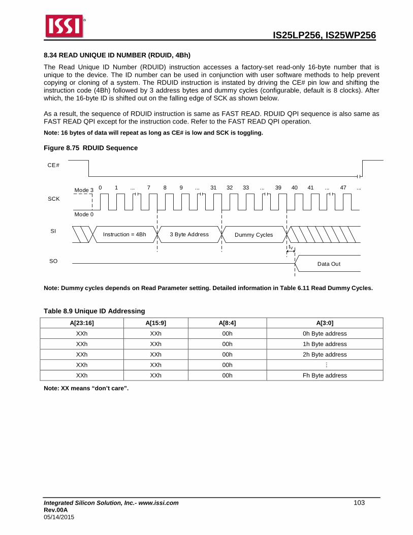
IS25LP256, IS25WP256
Integrated Silicon Solution, Inc.- www.issi.com 103 Rev.00A 05/14/2015
8.34 READ UNIQUE ID NUMBER (RDUID, 4Bh)
The Read Unique ID Number (RDUID) instruction accesses a factory-set read-only 16-byte number that is unique to the device. The ID number can be used in conjunction with user software methods to help prevent copying or cloning of a system. The RDUID instruction is instated by driving the CE# pin low and shifting the instruction code (4Bh) followed by 3 address bytes and dummy cycles (configurable, default is 8 clocks). After which, the 16-byte ID is shifted out on the falling edge of SCK as shown below. As a result, the sequence of RDUID instruction is same as FAST READ. RDUID QPI sequence is also same as FAST READ QPI except for the instruction code. Refer to the FAST READ QPI operation.
Note: 16 bytes of data will repeat as long as CE# is low and SCK is toggling. Figure 8.75 RDUID Sequence
Instruction = 4Bh Dummy Cycles
CE#
SCK
SI
SO
0 1 ... 7 8 9 ... 31 32 33 ... 39 40 41 ... 47Mode 3
Mode 0
3 Byte Address
Data Out
tV
...
Note: Dummy cycles depends on Read Parameter setting. Detailed information in Table 6.11 Read Dummy Cycles. Table 8.9 Unique ID Addressing
A[23:16] A[15:9] A[8:4] A[3:0]
XXh XXh 00h 0h Byte address
XXh XXh 00h 1h Byte address
XXh XXh 00h 2h Byte address
XXh XXh 00h …
XXh XXh 00h Fh Byte address
Note: XX means “don’t care”.

IS25LP256, IS25WP256
Integrated Silicon Solution, Inc.- www.issi.com 104 Rev.00A 05/14/2015
8.35 READ SFDP OPERATION (RDSFDP, 5Ah)
The Serial Flash Discoverable Parameters (SFDP) standard provides a consistent method of describing the functions and features of serial Flash devices in a standard set of internal parameter tables. These parameters can be interrogated by host system software to enable adjustments needed to accommodate divergent features from multiple vendors. For more details please refer to the JEDEC Standard JESD216A (Serial Flash Discoverable Parameters). The sequence of issuing RDSFDP instruction is same as FAST_READ: CE# goes low Send RDSFDP instruction (5Ah) Send 3 address bytes on SI pin Send dummy cycles (configurable, default is 8 clocks) on SI pin Read SFDP code on SO End RDSFDP operation by driving CE# high at any time during data out. Refer to ISSI’s Application note for SFDP table. The data at the addresses that are not specified in SFDP table are undefined. The sequence of RDSFDP instruction is same as FAST READ except for the instruction code. RDSFDP QPI sequence is also same as FAST READ QPI except for the instruction code. Refer to the FAST READ QPI operation. Figure 8.76 RDSFDP (Read SFDP) Sequence
Instruction = 5Ah Dummy Cycles
CE#
SCK
SI
SO
0 1 ... 7 8 9 ... 31 32 33 ... 39 40 41 ... 47Mode 3
Mode 0
3 Byte Address
Data Out
tV
...
Note: Dummy cycles depends on Read Parameter setting. Detailed information in Table 6.11 Read Dummy Cycles.
8.36 NO OPERATION (NOP, 00h)
The No Operation command solely cancels a Reset Enable command and has no impact on any other commands. It is available in both SPI and QPI modes. To execute a NOP, the host drives CE# low, sends the NOP command cycle (00H), then drives CE# high.
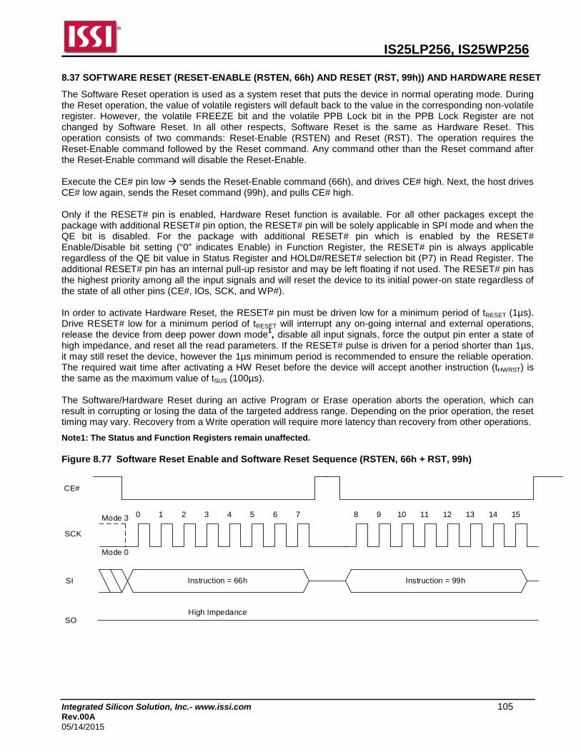
IS25LP256, IS25WP256
Integrated Silicon Solution, Inc.- www.issi.com 105 Rev.00A 05/14/2015
8.37 SOFTWARE RESET (RESET-ENABLE (RSTEN, 66h) AND RESET (RST, 99h)) AND HARDWARE RESET
The Software Reset operation is used as a system reset that puts the device in normal operating mode. During the Reset operation, the value of volatile registers will default back to the value in the corresponding non-volatile register. However, the volatile FREEZE bit and the volatile PPB Lock bit in the PPB Lock Register are not changed by Software Reset. In all other respects, Software Reset is the same as Hardware Reset. This operation consists of two commands: Reset-Enable (RSTEN) and Reset (RST). The operation requires the Reset-Enable command followed by the Reset command. Any command other than the Reset command after the Reset-Enable command will disable the Reset-Enable. Execute the CE# pin low sends the Reset-Enable command (66h), and drives CE# high. Next, the host drives CE# low again, sends the Reset command (99h), and pulls CE# high. Only if the RESET# pin is enabled, Hardware Reset function is available. For all other packages except the package with additional RESET# pin option, the RESET# pin will be solely applicable in SPI mode and when the QE bit is disabled. For the package with additional RESET# pin which is enabled by the RESET# Enable/Disable bit setting (“0” indicates Enable) in Function Register, the RESET# pin is always applicable regardless of the QE bit value in Status Register and HOLD#/RESET# selection bit (P7) in Read Register. The additional RESET# pin has an internal pull-up resistor and may be left floating if not used. The RESET# pin has the highest priority among all the input signals and will reset the device to its initial power-on state regardless of the state of all other pins (CE#, IOs, SCK, and WP#). In order to activate Hardware Reset, the RESET# pin must be driven low for a minimum period of tRESET (1µs). Drive RESET# low for a minimum period of tRESET will interrupt any on-going internal and external operations, release the device from deep power down mode1, disable all input signals, force the output pin enter a state of high impedance, and reset all the read parameters. If the RESET# pulse is driven for a period shorter than 1µs, it may still reset the device, however the 1µs minimum period is recommended to ensure the reliable operation. The required wait time after activating a HW Reset before the device will accept another instruction (tHWRST) is the same as the maximum value of tSUS (100µs). The Software/Hardware Reset during an active Program or Erase operation aborts the operation, which can result in corrupting or losing the data of the targeted address range. Depending on the prior operation, the reset timing may vary. Recovery from a Write operation will require more latency than recovery from other operations.
Note1: The Status and Function Registers remain unaffected. Figure 8.77 Software Reset Enable and Software Reset Sequence (RSTEN, 66h + RST, 99h)
Instruction = 66h
CE#
SCK
SI
0 1Mode 3
Mode 0
2 3 4 5 6 7
Instruction = 99h
8 9 10 11 12 13 14 15
SOHigh Impedance
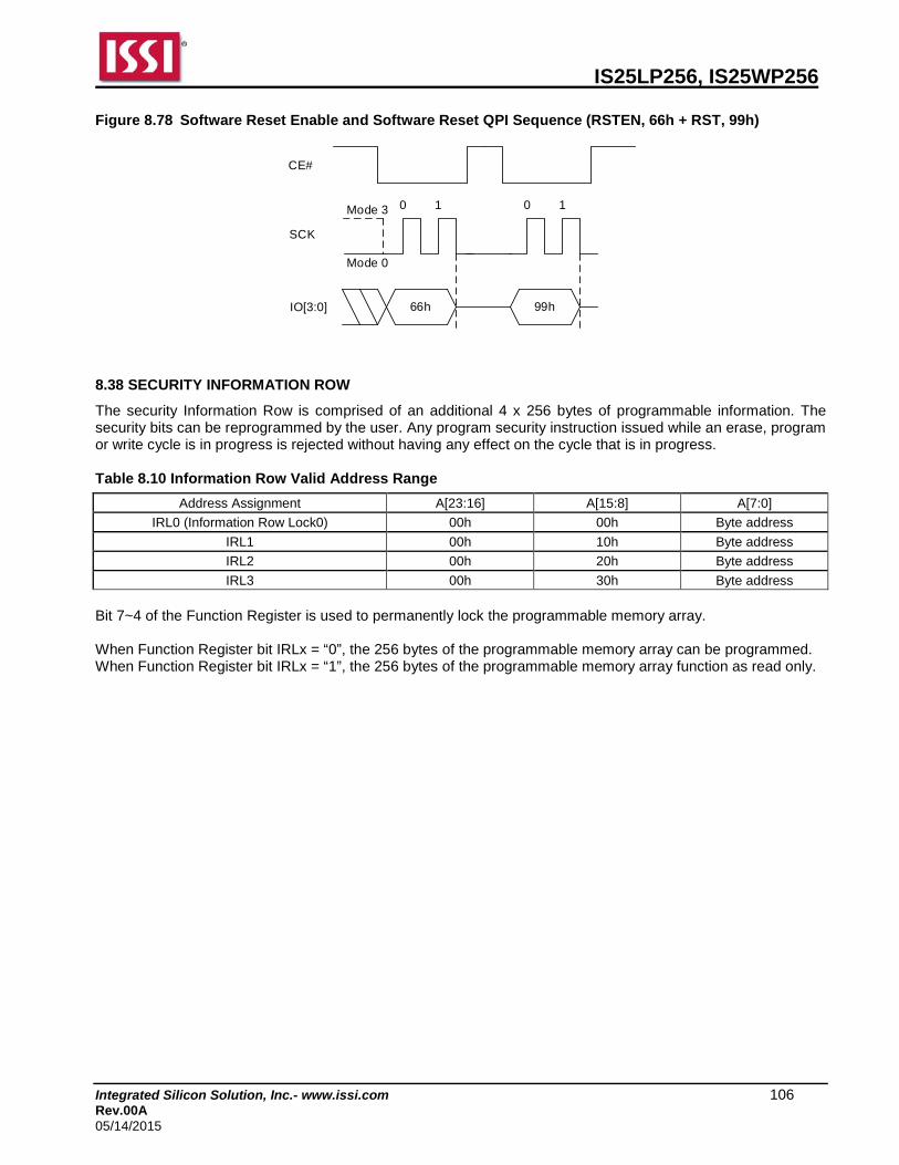
IS25LP256, IS25WP256
Integrated Silicon Solution, Inc.- www.issi.com 106 Rev.00A 05/14/2015
Figure 8.78 Software Reset Enable and Software Reset QPI Sequence (RSTEN, 66h + RST, 99h)
66h
CE#
SCK
IO[3:0]
0 1Mode 3
Mode 0
99h
0 1
8.38 SECURITY INFORMATION ROW
The security Information Row is comprised of an additional 4 x 256 bytes of programmable information. The security bits can be reprogrammed by the user. Any program security instruction issued while an erase, program or write cycle is in progress is rejected without having any effect on the cycle that is in progress. Table 8.10 Information Row Valid Address Range
Address Assignment A[23:16] A[15:8] A[7:0] IRL0 (Information Row Lock0) 00h 00h Byte address
IRL1 00h 10h Byte address IRL2 00h 20h Byte address
IRL3 00h 30h Byte address Bit 7~4 of the Function Register is used to permanently lock the programmable memory array. When Function Register bit IRLx = “0”, the 256 bytes of the programmable memory array can be programmed. When Function Register bit IRLx = “1”, the 256 bytes of the programmable memory array function as read only.
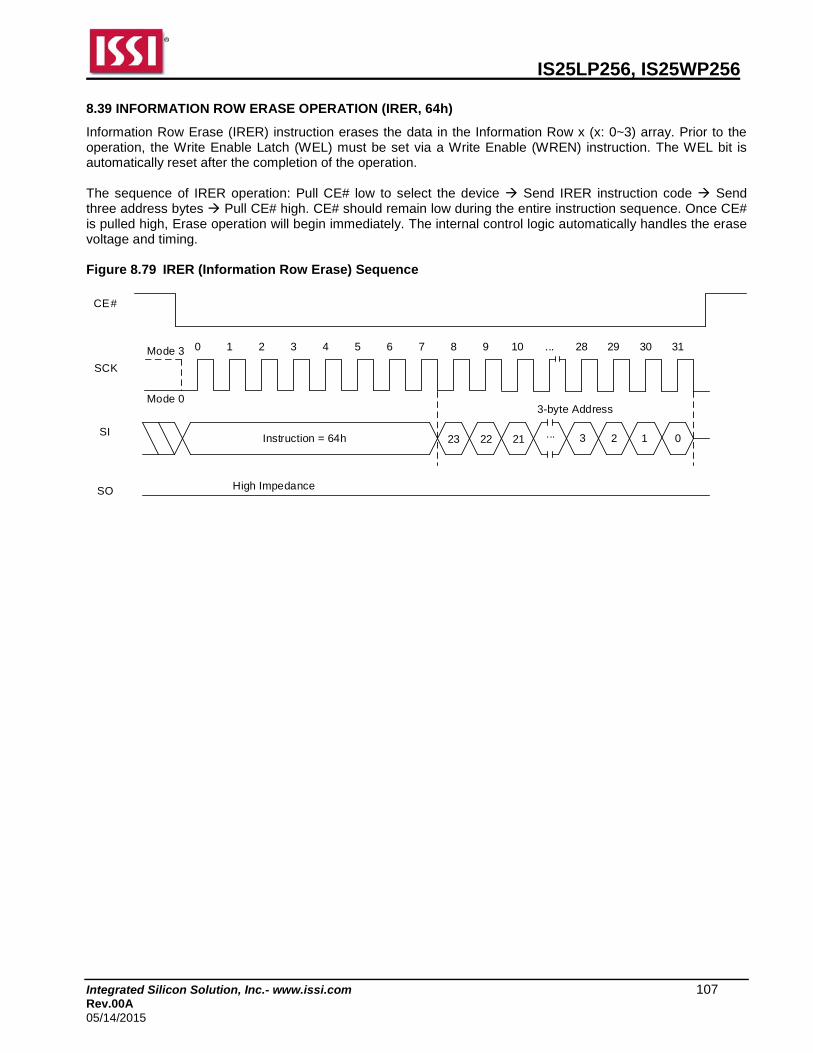
IS25LP256, IS25WP256
Integrated Silicon Solution, Inc.- www.issi.com 107 Rev.00A 05/14/2015
8.39 INFORMATION ROW ERASE OPERATION (IRER, 64h)
Information Row Erase (IRER) instruction erases the data in the Information Row x (x: 0~3) array. Prior to the operation, the Write Enable Latch (WEL) must be set via a Write Enable (WREN) instruction. The WEL bit is automatically reset after the completion of the operation. The sequence of IRER operation: Pull CE# low to select the device Send IRER instruction code Send three address bytes Pull CE# high. CE# should remain low during the entire instruction sequence. Once CE# is pulled high, Erase operation will begin immediately. The internal control logic automatically handles the erase voltage and timing. Figure 8.79 IRER (Information Row Erase) Sequence
Instruction = 64h 23
CE#
SCK
SI 3 2
SO
1 0
3-byte Address
High Impedance
22 21 ...
0 1 2 3 4 5 6 7 8 9 10 ... 28 29 30 31Mode 3
Mode 0
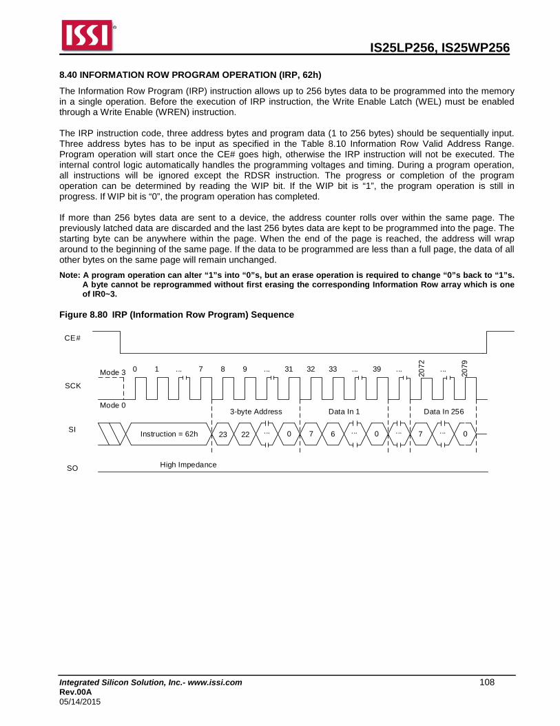
IS25LP256, IS25WP256
Integrated Silicon Solution, Inc.- www.issi.com 108 Rev.00A 05/14/2015
8.40 INFORMATION ROW PROGRAM OPERATION (IRP, 62h)
The Information Row Program (IRP) instruction allows up to 256 bytes data to be programmed into the memory in a single operation. Before the execution of IRP instruction, the Write Enable Latch (WEL) must be enabled through a Write Enable (WREN) instruction. The IRP instruction code, three address bytes and program data (1 to 256 bytes) should be sequentially input. Three address bytes has to be input as specified in the Table 8.10 Information Row Valid Address Range. Program operation will start once the CE# goes high, otherwise the IRP instruction will not be executed. The internal control logic automatically handles the programming voltages and timing. During a program operation, all instructions will be ignored except the RDSR instruction. The progress or completion of the program operation can be determined by reading the WIP bit. If the WIP bit is “1”, the program operation is still in progress. If WIP bit is “0”, the program operation has completed. If more than 256 bytes data are sent to a device, the address counter rolls over within the same page. The previously latched data are discarded and the last 256 bytes data are kept to be programmed into the page. The starting byte can be anywhere within the page. When the end of the page is reached, the address will wrap around to the beginning of the same page. If the data to be programmed are less than a full page, the data of all other bytes on the same page will remain unchanged.
Note: A program operation can alter “1”s into “0”s, but an erase operation is required to change “0”s back to “1”s. A byte cannot be reprogrammed without first erasing the corresponding Information Row array which is one of IR0~3.
Figure 8.80 IRP (Information Row Program) Sequence
Instruction = 62h 23
CE#
SCK
SI 7 6
SO
7
3-byte Address
High Impedance
22 ... 0
Data In 1 Data In 256
0 1 ... 7 8 9 ... 31 32 33 ... 39 ...
2072 ...
2079
Mode 3
Mode 0
... 0 ... ... 0

IS25LP256, IS25WP256
Integrated Silicon Solution, Inc.- www.issi.com 109 Rev.00A 05/14/2015
8.41 INFORMATION ROW READ OPERATION (IRRD, 68h)
The IRRD instruction is used to read memory data at up to a 166MHz clock. The IRRD instruction code is followed by three address bytes (A23 - A0) and dummy cycles (configurable, default is 8 clocks), transmitted via the SI line, with each bit latched-in during the rising edge of SCK. Then the first data byte addressed is shifted out on the SO line, with each bit shifted out at a maximum frequency fCT, during the falling edge of SCK. The address is automatically incremented by one after each byte of data is shifted out. Once the address reaches the last address of each 256 byte Information Row, the next address will not be valid and the data of the address will be garbage data. It is recommended to repeat four times IRRD operation that reads 256 byte with a valid starting address of each Information Row in order to read all data in the 4 x 256 byte Information Row array. The IRRD instruction is terminated by driving CE# high (VIH). If an IRRD instruction is issued while an Erase, Program or Write cycle is in process (WIP=1) the instruction is ignored and will not have any effects on the current cycle The sequence of IRRD instruction is same as Fast Read except for the instruction code. IRRD QPI sequence is same as Fast Read QPI except for the instruction code. Refer to the Fast Read QPI operation. Figure 8.81 IRRD (Information Row Read) Sequence
Instruction = 68h Dummy Cycles
CE#
SCK
SI
SO
0 1 ... 7 8 9 ... 31 32 33 ... 39 40 41 ... 47Mode 3
Mode 0
3 Byte Address
Data Out
tV
...
Note: Dummy cycles depends on Read Parameter setting. Detailed information in Table 6.11 Read Dummy Cycles.

IS25LP256, IS25WP256
Integrated Silicon Solution, Inc.- www.issi.com 110 Rev.00A 05/14/2015
8.42 FAST READ DTR MODE OPERATION (FRDTR, 0Dh or 4FRDTR, 0Eh)
The FRDTR/4FRDTR instruction is for doubling the data in and out. Signals are triggered on both rising and falling edge of clock. The address is latched on both rising and falling edge of SCK, and data of each bit shifts out on both rising and falling edge of SCK at a maximum frequency fC2. The 2-bit address can be latched-in at one clock, and 2-bit data can be read out at one clock, which means one bit at the rising edge of clock, the other bit at the falling edge of clock. The first address byte can be at any location. The address is automatically increased to the next higher address after each byte of data is shifted out, so the whole memory can be read out in a single FRDTR/4FRDTR instruction. The address counter rolls over to 0 when the highest address is reached. • 0Dh (EXTADD=0) is followed by a 3-byte address (A23-A0) or • 0Dh (EXTADD=1) is followed by a 4-byte address (A31-A0) or • 0Eh is followed by a 4-byte address (A31-A0) The sequence of issuing FRDTR/4FRDTR instruction is: CE# goes low Sending FRDTR/4FRDTR instruction code (1bit per clock) 3-byte or 4-byte address on SI (2-bit per clock) as above 8 dummy clocks (configurable, default is 8 clocks) on SI Data out on SO (2-bit per clock) End FRDTR/4FRDTR operation via driving CE# high at any time during data out. While a Program/Erase/Write Status Register cycle is in progress, FRDTR/4FRDTR instruction will be rejected without any effect on the current cycle.
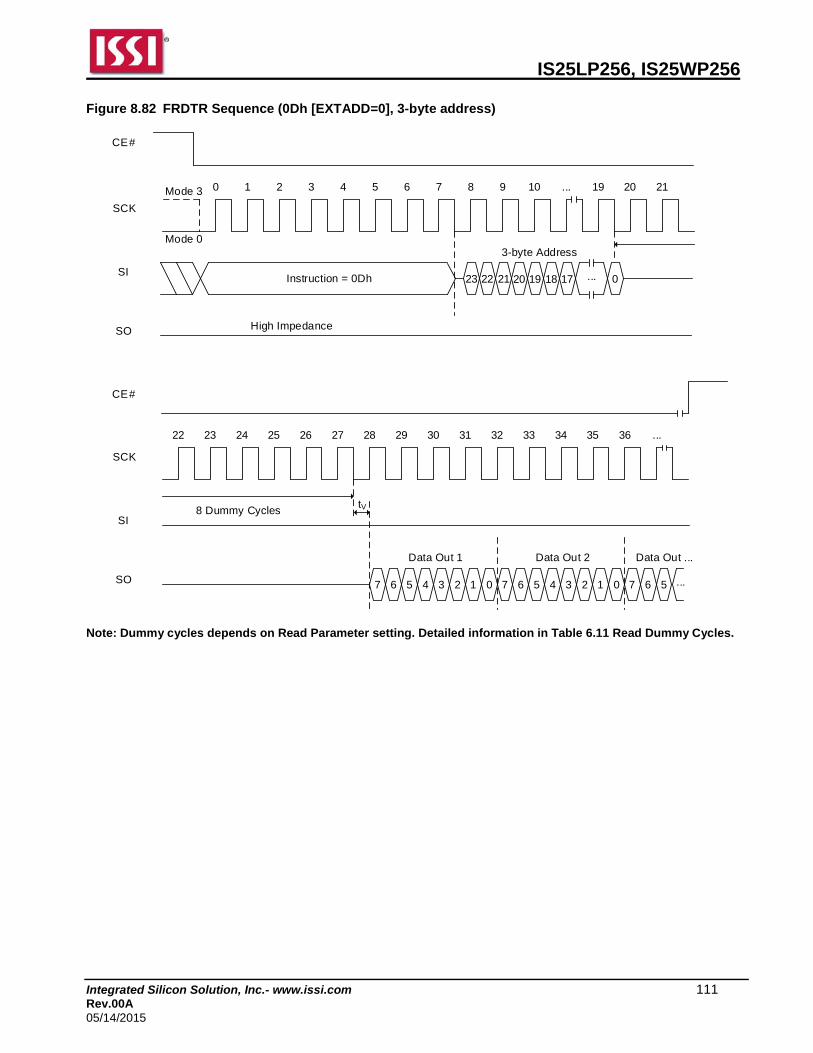
IS25LP256, IS25WP256
Integrated Silicon Solution, Inc.- www.issi.com 111 Rev.00A 05/14/2015
Figure 8.82 FRDTR Sequence (0Dh [EXTADD=0], 3-byte address)
CE#
SCK
SI
SO
Data Out 1
Instruction = 0Dh
CE#
SCK
SI
SO
3-byte Address
High Impedance
0 1 2 3 4 5 6 7 8 9 10 ... 19 20 21
22 23 24 25 26 27 28 29 30 31 32 33 34 35 36 ...
Mode 3
Mode 0
tV
23 22 21 0
7 6 5 4 3 2 1 0
Data Out 2
7 6 5 4 3 2 1 0
Data Out ...
7 6
8 Dummy Cycles
20 19 18 17
5 ...
...
Note: Dummy cycles depends on Read Parameter setting. Detailed information in Table 6.11 Read Dummy Cycles.

IS25LP256, IS25WP256
Integrated Silicon Solution, Inc.- www.issi.com 112 Rev.00A 05/14/2015
Figure 8.83 FRDTR Sequence (0Dh [EXTADD=1] or 0Eh, 4-byte address)
Instruction = 0Dh/0Eh
4-byte Address
27 28 29
30 31 32 33 34 35 36 37 38 39 40 41 42 43 44 ...
31 30 29 28 27 26 25
CE#
SCK
SI
SO
Data Out 1
CE#
SCK
SI
SO High Impedance
0 1 2 3 4 5 6 7 8 9 10 ...Mode 3
Mode 0
tV
0
7 6 5 4 3 2 1 0
Data Out 2
7 6 5 4 3 2 1 0
Data Out ...
7 6
8 Dummy Cycles
5 ...
...
Note: Dummy cycles depends on Read Parameter setting. Detailed information in Table 6.11 Read Dummy Cycles.

IS25LP256, IS25WP256
Integrated Silicon Solution, Inc.- www.issi.com 113 Rev.00A 05/14/2015
FAST READ DTR QPI MODE OPERATION (FRDTR QPI, 0Dh or 4FRDTR QPI, 0Eh)
The FRDTR/4FRDTR QPI instruction utilizes all four IO lines to input the instruction code so that only two clocks are required, while the FRDTR/4FRDTR instruction requires that the byte-long instruction code is shifted into the device only via IO0 (SI) line in eight clocks. In addition, subsequent address and data out are shifted in/out via all four IO lines unlike the FRDTR/4FRDTR instruction. Eventually this operation is same as the FRQDTR/4FRQDTR QPI, but the only different thing is that AX mode is not available in the FRDTR/4FRDTR QPI operation. A Quad Enable (QE) bit of Status Register must be set to "1" before sending the FRDTR/4FRDTR QPI instruction. • 0Dh (EXTADD=0) is followed by a 3-byte address (A23-A0) or • 0Dh (EXTADD=1) is followed by a 4-byte address (A31-A0) or • 0Eh is followed by a 4-byte address (A31-A0) The sequence of issuing FRDTR/4FRDTR QPI instruction is: CE# goes low Sending FRDTR/4FRDTR QPI instruction (4-bit per clock) 24-bit or 32-bit address interleave on IO3, IO2, IO1 & IO0 (8-bit per clock) as above 6 dummy clocks (configurable, default is 6 clocks) Data out interleave on IO3, IO2, IO1 & IO0 (8-bit per clock) End FRDTR/4FRDTR QPI operation by driving CE# high at any time during data out. If the FRDTR/4FRDTR QPI instruction is issued while an Erase, Program or Write cycle is in process is in progress (WIP=1), the instruction will be rejected without any effect on the current cycle. Figure 8.84 FRDTR QPI Sequence (0Dh [EXTADD=0], 3-byte address)
Instruction= 0Dh
CE#
SCK
3-byte Address
0 1 2 3 4 5 6 7 8 9 10 11 12Mode 3
Mode 0tV
20 16 12
5 121 17 13
4 0IO0
IO1
22 18 14
23 19 15
8 4 0
9 5 1
10 6 2
11 7 3
6 Dummy Cycles
IO2
IO3
6 2
7 3
5 1
4 0
6 2
7 3
DataOut
DataOut
...
4 0
5 1
6 2
7 3
...
...
...
...
Notes: 1. Number of dummy cycles depends on clock speed. Detailed information in Table 6.11 Read Dummy Cycles. 2. Sufficient dummy cycles are required to avoid I/O contention.
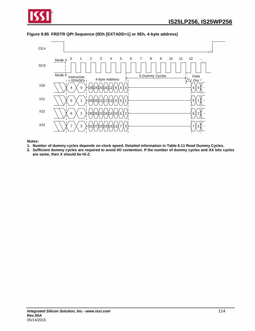
IS25LP256, IS25WP256
Integrated Silicon Solution, Inc.- www.issi.com 114 Rev.00A 05/14/2015
Figure 8.85 FRDTR QPI Sequence (0Dh [EXTADD=1] or 0Eh, 4-byte address)
Instruction= 0Dh/0Eh
CE#
SCK
0 1 2 3 4 5 6 7 8 9 10 11 12Mode 3
Mode 0
IO0
IO1
6 Dummy Cycles
IO2
IO3
...
4 0
5 1
6 2
7 3
4-byte Address tV
28 24 20
5 125 21
4 0
30 26 22
31 27 23
16 12 8
17 13 9
18 14 10
19 15 11
6 2
7 3
DataOut
...
...
...
...
4 0
5 1
6 2
7 3
29
Notes: 1. Number of dummy cycles depends on clock speed. Detailed information in Table 6.11 Read Dummy Cycles. 2. Sufficient dummy cycles are required to avoid I/O contention. If the number of dummy cycles and AX bits cycles
are same, then X should be Hi-Z.

IS25LP256, IS25WP256
Integrated Silicon Solution, Inc.- www.issi.com 115 Rev.00A 05/14/2015
8.43 FAST READ DUAL IO DTR MODE OPERATION (FRDDTR, BDh or 4FRDDTR, BEh)
The FRDDTR/4FRDDTR instruction enables Double Transfer Rate throughput on dual I/O of the device in read mode. The address (interleave on dual I/O pins) is latched on both rising and falling edge of SCK, and the data (interleave on dual I/O pins) shift out on both rising and falling edge of SCK at a maximum frequency fT2. The 4-bit address can be latched-in at one clock, and 4-bit data can be read out at one clock, which means two bits at the rising edge of clock, the other two bits at the falling edge of clock. The first address byte can be at any location. The address is automatically increased to the next higher address after each byte of data is shifted out, so the whole memory can be read out with a single FRDDTR/4FRDDTR instruction. The address counter rolls over to 0 when the highest address is reached. Once writing FRDDTR/4FRDDTR instruction, the following address/dummy/data out will perform as 4-bit instead of previous 1-bit. • BDh (EXTADD=0) is followed by a 3-byte address (A23-A0) or • BDh (EXTADD=1) is followed by a 4-byte address (A31-A0) or • BEh is followed by a 4-byte address (A31-A0) The sequence of issuing FRDDTR/4FRDDTR instruction is: CE# goes low Sending FRDDTR/4FRDDTR instruction (1-bit per clock) 24-bit or 32-bit address interleave on IO1 & IO0 (4-bit per clock) as above 4 dummy clocks (configurable, default is 4 clocks) on IO1 & IO0 Data out interleave on IO1 & IO0 (4-bit per clock) End FRDDTR/4FRDDTR operation via pulling CE# high at any time during data out (Please refer to Figures 8.86 and 8.87 for 2 x I/O Double Transfer Rate Read Mode Timing Waveform). If AXh (where X is don’t care) is input for the mode bits during dummy cycles, the device will enter AX read operation mode which enables subsequent FRDDTR/4FRDDTR execution skips command code. It saves cycles as described in Figures 8.88 and 8.89. When the code is different from AXh (where X is don’t care), the device exits the AX read operation. After finishing the read operation, device becomes ready to receive a new command. If the FRDDTR/4FRDDTR instruction is issued while an Erase, Program or Write cycle is in process is in progress (WIP=1), the instruction will be rejected without any effect on the current cycle.

IS25LP256, IS25WP256
Integrated Silicon Solution, Inc.- www.issi.com 116 Rev.00A 05/14/2015
Figure 8.86 FRDDTR Sequence (BDh [EXTADD=0], 3-byte address)
CE#
SCK
SI
SO
Instruction = BDh
CE#
SCK
SI
SO
3-byte Address
High Impedance
0 1 2 3 4 5 6 7 8 9 10 ... 13 14
15 16 17 18 19 20 21 22 23 24 25 26 27 28 29
Mode 3
Mode 0
...
tV
22 20 18 0
7 5 3 1 7 5 3 1 7 5 3 1 7 5 3 1 7 5 3 1 7 5 3 1
4 Dummy Cycles
23 21 19 1
Data Out
...6 4 2 0 6 4 2 0 6 4 2 0 6 4 2 0 6 4 2 0 6 4 2 0
Data Out Data Out Data Out Data Out Data Out
16 14 12
17 15 13
10
11 7 5
6 4
3 1
2 0
Mode Bits
...
Mode Bits
...
...
Notes: 1. If the mode bits=AXh (where X is don’t care), it can execute the AX read mode (without command). When the
mode bits are different from AXh, the device exits the AX read operation. 2. Number of dummy cycles depends on clock speed. Detailed information in Table 6.11 Read Dummy Cycles. 3. Sufficient dummy cycles are required to avoid I/O contention. If the number of dummy cycles and AX bits cycles
are same, then X should be Hi-Z.

IS25LP256, IS25WP256
Integrated Silicon Solution, Inc.- www.issi.com 117 Rev.00A 05/14/2015
Figure 8.87 FRDDTR Sequence (BDh [EXTADD=1] or BEh, 4-byte address)
CE#
SCK
SI
SO
Instruction = BDh/BEh
CE#
SCK
SI
SO
4-byte Address
High Impedance
0 1 2 3 4 5 6 7 8 9 10 ... 17 18
19 20 21 22 23 24 25 26 27 28 29 30 31 32 33
Mode 3
Mode 0
tV
30 28 26 0
7 5 3 1 7 5 3 1 7 5 3 1 7 5 3 1 7 5 3 1 7 5 3 1
4 Dummy Cycles
31 29 27 1
Data Out
...6 4 2 0 6 4 2 0 6 4 2 0 6 4 2 0 6 4 2 0 6 4 2 0
Data Out Data Out Data Out Data Out Data Out
24 22 20
25 23 21
18
19 7 5
6 4
3 1
2 0
Mode Bits
...
Mode Bits
...
...
...
Notes: 1. If the mode bits=AXh (where X is don’t care), it can execute the AX read mode (without command). When the
mode bits are different from AXh, the device exits the AX read operation. 2. Number of dummy cycles depends on clock speed. Detailed information in Table 6.11 Read Dummy Cycles. 3. Sufficient dummy cycles are required to avoid I/O contention. If the number of dummy cycles and AX bits cycles
are same, then X should be Hi-Z.
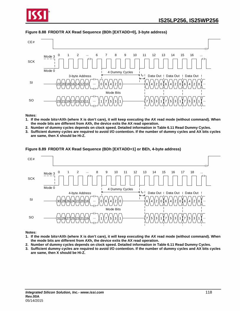
IS25LP256, IS25WP256
Integrated Silicon Solution, Inc.- www.issi.com 118 Rev.00A 05/14/2015
Figure 8.88 FRDDTR AX Read Sequence (BDh [EXTADD=0], 3-byte address)
SI
SO
3-byte Address
...
...
tV
22 20 18
7 5 3 1 7 5 3 1 7 5 3 1
4 Dummy Cycles
23 21 19
...6 4 2 0 6 4 2 0 6 4 2 0
Data Out Data Out Data Out
16 14 12
17 15 13
10
11
SCK
0 1 2 ... 6 7 8 9 10 11 12 13 14 15 16Mode 3
Mode 0
CE#
7 5 3 1
6 4 2 00
1
Mode Bits
...
...
Notes: 1. If the mode bits=AXh (where X is don’t care), it will keep executing the AX read mode (without command). When
the mode bits are different from AXh, the device exits the AX read operation. 2. Number of dummy cycles depends on clock speed. Detailed information in Table 6.11 Read Dummy Cycles. 3. Sufficient dummy cycles are required to avoid I/O contention. If the number of dummy cycles and AX bits cycles
are same, then X should be Hi-Z. Figure 8.89 FRDDTR AX Read Sequence (BDh [EXTADD=1] or BEh, 4-byte address)
4-byte Address
...
30 28 26
31 29 27
24 22 20
25 23 21
18
19
8 9 10 11 12 13 14 15 16 17 18
SI
SO ...
tV
7 5 3 1 7 5 3 1 7 5 3 1
4 Dummy Cycles
...6 4 2 0 6 4 2 0 6 4 2 0
Data Out Data Out Data Out
SCK
0 1 2 ...Mode 3
Mode 0
CE#
7 5 3 1
6 4 2 00
1
Mode Bits
...
...
Notes: 1. If the mode bits=AXh (where X is don’t care), it will keep executing the AX read mode (without command). When
the mode bits are different from AXh, the device exits the AX read operation. 2. Number of dummy cycles depends on clock speed. Detailed information in Table 6.11 Read Dummy Cycles. 3. Sufficient dummy cycles are required to avoid I/O contention. If the number of dummy cycles and AX bits cycles
are same, then X should be Hi-Z.
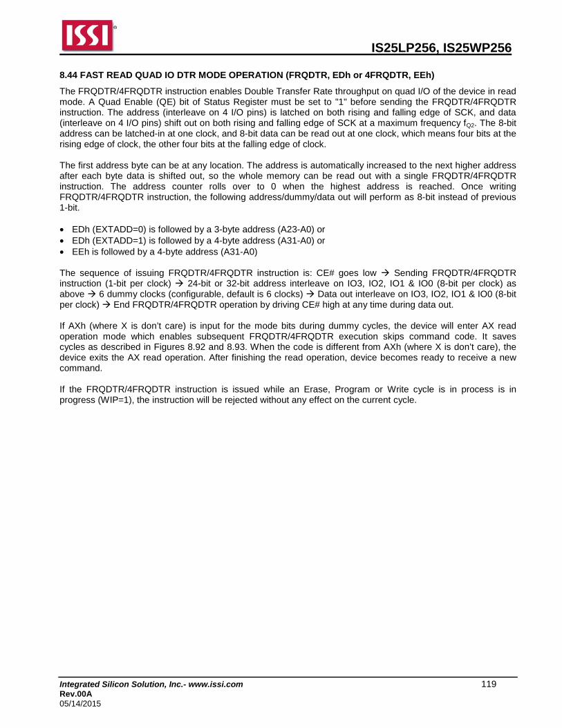
IS25LP256, IS25WP256
Integrated Silicon Solution, Inc.- www.issi.com 119 Rev.00A 05/14/2015
8.44 FAST READ QUAD IO DTR MODE OPERATION (FRQDTR, EDh or 4FRQDTR, EEh)
The FRQDTR/4FRQDTR instruction enables Double Transfer Rate throughput on quad I/O of the device in read mode. A Quad Enable (QE) bit of Status Register must be set to "1" before sending the FRQDTR/4FRQDTR instruction. The address (interleave on 4 I/O pins) is latched on both rising and falling edge of SCK, and data (interleave on 4 I/O pins) shift out on both rising and falling edge of SCK at a maximum frequency fQ2. The 8-bit address can be latched-in at one clock, and 8-bit data can be read out at one clock, which means four bits at the rising edge of clock, the other four bits at the falling edge of clock. The first address byte can be at any location. The address is automatically increased to the next higher address after each byte data is shifted out, so the whole memory can be read out with a single FRQDTR/4FRQDTR instruction. The address counter rolls over to 0 when the highest address is reached. Once writing FRQDTR/4FRQDTR instruction, the following address/dummy/data out will perform as 8-bit instead of previous 1-bit. • EDh (EXTADD=0) is followed by a 3-byte address (A23-A0) or • EDh (EXTADD=1) is followed by a 4-byte address (A31-A0) or • EEh is followed by a 4-byte address (A31-A0) The sequence of issuing FRQDTR/4FRQDTR instruction is: CE# goes low Sending FRQDTR/4FRQDTR instruction (1-bit per clock) 24-bit or 32-bit address interleave on IO3, IO2, IO1 & IO0 (8-bit per clock) as above 6 dummy clocks (configurable, default is 6 clocks) Data out interleave on IO3, IO2, IO1 & IO0 (8-bit per clock) End FRQDTR/4FRQDTR operation by driving CE# high at any time during data out. If AXh (where X is don’t care) is input for the mode bits during dummy cycles, the device will enter AX read operation mode which enables subsequent FRQDTR/4FRQDTR execution skips command code. It saves cycles as described in Figures 8.92 and 8.93. When the code is different from AXh (where X is don’t care), the device exits the AX read operation. After finishing the read operation, device becomes ready to receive a new command. If the FRQDTR/4FRQDTR instruction is issued while an Erase, Program or Write cycle is in process is in progress (WIP=1), the instruction will be rejected without any effect on the current cycle.

IS25LP256, IS25WP256
Integrated Silicon Solution, Inc.- www.issi.com 120 Rev.00A 05/14/2015
Figure 8.90 FRQDTR Sequence (EDh [EXTADD=0], 3-byte address)
CE#
SCK
Instruction = EDh
CE#
SCK
3-byte Address
High Impedance
0 1 2 3 4 5 6 7 8 9 10 11 12
14 15 16 17 18 19 20 21 22 23 24 25 26 ...
Mode 3
Mode 0
tV
20 16 12
5 1
21 17 13
DataOut
4 0
IO0
IO1
IO0
22 18 14
23 19 15
8 4 0
9 5 1
10 6 2
11 7 3
6 Dummy Cycles
IO2
IO3
IO1
IO2
IO3
6 2
7 3
5 1
4 0
6 2
7 3
5 1
4 0
6 2
7 3
5 1
4 0
6 2
7 3
5 1
4 0
6 2
7 3
5 1
4 0
6 2
7 3
5 1
4 0
6 2
7 3
5 1
4 0
6 2
7 3
5 1
4 0
6 2
7 3
5 1
4 0
6 2
7 3
DataOut
DataOut
DataOut
DataOut
DataOut
DataOut
DataOut
DataOut
DataOut
13
5 1
4 0
6 2
7 3
Mode Bits
...
...
...
...
Notes: 1. If the mode bits=AXh (where X is don’t care), it can execute the AX read mode (without command). When the
mode bits are different from AXh, the device exits the AX read operation. 2. Number of dummy cycles depends on clock speed. Detailed information in Table 6.11 Read Dummy Cycles. 3. Sufficient dummy cycles are required to avoid I/O contention. If the number of dummy cycles and AX bits cycles
are same, then X should be Hi-Z.

IS25LP256, IS25WP256
Integrated Silicon Solution, Inc.- www.issi.com 121 Rev.00A 05/14/2015
Figure 8.91 FRQDTR Sequence (EDh [EXTADD=1] or EEh, 4-byte address)
CE#
SCK
Instruction = EDh/EEh
CE#
SCK
4-byte Address
High Impedance
0 1 2 3 4 5 6 7 8 9 10 11 12
15 16 17 18 19 20 21 22 23 24 25 26 27 ...
Mode 3
Mode 0
tV
28 24 20
5 1
29 25 21
DataOut
...4 0
IO0
IO1
IO0
30 26 22
31 27 23
16 12 8
17 13 9
18 14 10
19 15 11
6 Dummy Cycles
IO2
IO3
IO1
IO2
IO3
6 2
7 3
5 1
4 0
6 2
7 3
5 1
4 0
6 2
7 3
5 1
4 0
6 2
7 3
5 1
4 0
6 2
7 3
5 1
4 0
6 2
7 3
5 1
4 0
6 2
7 3
5 1
4 0
6 2
7 3
5 1
4 0
6 2
7 3
5 1
4 0
6 2
7 3
DataOut
DataOut
DataOut
DataOut
DataOut
DataOut
DataOut
DataOut
DataOut
14
5 1
4 0
6 2
7 3
Mode Bits
13
5 1
4 0
6 2
7 3
...
...
...
Notes: 1. If the mode bits=AXh (where X is don’t care), it can execute the AX read mode (without command). When the
mode bits are different from AXh, the device exits the AX read operation. 2. Number of dummy cycles depends on clock speed. Detailed information in Table 6.11 Read Dummy Cycles. 3. Sufficient dummy cycles are required to avoid I/O contention. If the number of dummy cycles and AX bits cycles
are same, then X should be Hi-Z.
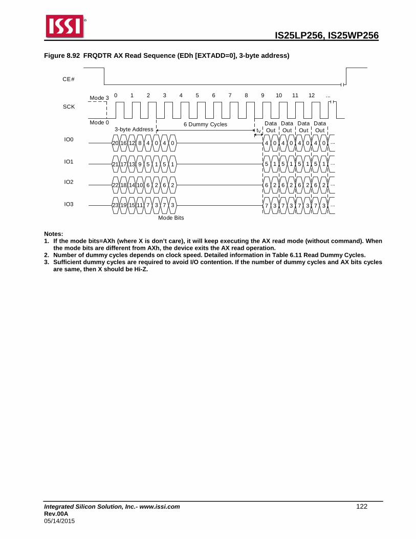
IS25LP256, IS25WP256
Integrated Silicon Solution, Inc.- www.issi.com 122 Rev.00A 05/14/2015
Figure 8.92 FRQDTR AX Read Sequence (EDh [EXTADD=0], 3-byte address)
CE#
SCK
3-byte Address
0 1 2 3 4 5 6 7 8 9 10 11Mode 3
Mode 0tV
20 16 12
5 121 17 13
4 0IO0
IO1
22 18 14
23 19 15
8 4 0
9 5 1
10 6 2
11 7 3
6 Dummy Cycles
IO2
IO3
6 2
7 3
5 1
4 0
6 2
7 3
5 1
4 0
6 2
7 3
5 1
4 0
6 2
7 3
DataOut
DataOut
DataOut
DataOut
5 1
4 0
6 2
7 3
Mode Bits
12 ...
...
...
...
...
Notes: 1. If the mode bits=AXh (where X is don’t care), it will keep executing the AX read mode (without command). When
the mode bits are different from AXh, the device exits the AX read operation. 2. Number of dummy cycles depends on clock speed. Detailed information in Table 6.11 Read Dummy Cycles. 3. Sufficient dummy cycles are required to avoid I/O contention. If the number of dummy cycles and AX bits cycles
are same, then X should be Hi-Z.
IS25LP256, IS25WP256
Integrated Silicon Solution, Inc.- www.issi.com 123 Rev.00A 05/14/2015
Figure 8.93 FRQDTR AX Read Sequence (EDh [EXTADD=1] or EEh, 4-byte address)
CE#
SCK
4-byte Address
0 1 2 3 4 5 6 7 8 9 10 11Mode 3
Mode 0tV
28 24 20
5 129 25 21
4 0IO0
IO1
30 26 22
31 27 23
16 12 0
17 13 1
18 14 2
19 15 3
6 Dummy Cycles
IO2
IO3
6 2
7 3
5 1
4 0
6 2
7 3
5 1
4 0
6 2
7 3
5 1
4 0
6 2
7 3
DataOut
DataOut
DataOut
DataOut
5 1
4 0
6 2
7 3
Mode Bits
12 13 ...
8 4
9 5
10 6
11 7
...
...
...
...
Notes: 1. If the mode bits=AXh (where X is don’t care), it will keep executing the AX read mode (without command). When
the mode bits are different from AXh, the device exits the AX read operation. 2. Number of dummy cycles depends on clock speed. Detailed information in Table 6.11 Read Dummy Cycles. 3. Sufficient dummy cycles are required to avoid I/O contention. If the number of dummy cycles and AX bits cycles
are same, then X should be Hi-Z.
IS25LP256, IS25WP256
Integrated Silicon Solution, Inc.- www.issi.com 124 Rev.00A 05/14/2015
FAST READ QUAD IO DTR QPI MODE OPERATION (FRQDTR QPI, EDh OR 4FRQDTR QPI, EEh)
The FRQDTR/4FRQDTR QPI instruction utilizes all four IO lines to input the instruction code so that only two clocks are required, while the FRQDTR/4FRQDTR instruction requires that the byte-long instruction code is shifted into the device only via IO0 line in eight clocks. As a result, 6 command cycles will be reduced by the FRQDTR/4FRQDTR QPI instruction. In addition, subsequent address and data out are shifted in/out via all four IO lines like the FRQDTR/4FRQDTR instruction. In fact, except for the command cycle, the FRQDTR/4FRQDTR QPI operation is exactly same as the FRQDTR/4FRQDTR. A Quad Enable (QE) bit of Status Register must be set to "1" before sending the FRQDTR/4FRQDTR QPI instruction. • EDh (EXTADD=0) is followed by a 3-byte address (A23-A0) or • EDh (EXTADD=1) is followed by a 4-byte address (A31-A0) or • EEh is followed by a 4-byte address (A31-A0) The sequence of issuing FRQDTR/4FRQDTR QPI instruction is: CE# goes low Sending FRQDTR/4FRQDTR QPI instruction (4-bit per clock) 24-bit or 32-bit address interleave on IO3, IO2, IO1 & IO0 (8-bit per clock) as above 6 dummy clocks (configurable, default is 6 clocks) Data out interleave on IO3, IO2, IO1 & IO0 (8-bit per clock) End FRQDTR/4FRQDTR QPI operation by driving CE# high at any time during data out. If AXh (where X is don’t care) is input for the mode bits during dummy cycles, the device will enter AX read operation mode which enables subsequent FRQDTR/4FRQDTR QPI execution skips command code. It saves cycles as described in Figures 8.92 and 8.93. When the code is different from AXh (where X is don’t care), the device exits the AX read operation. After finishing the read operation, device becomes ready to receive a new command. If the FRQDTR/4FRQDTR QPI instruction is issued while an Erase, Program or Write cycle is in process is in progress (WIP=1), the instruction will be rejected without any effect on the current cycle.

IS25LP256, IS25WP256
Integrated Silicon Solution, Inc.- www.issi.com 125 Rev.00A 05/14/2015
Figure 8.94 FRQDTR QPI Sequence (EDh [EXTADD=0], 3-byte address)
Instruction= EDh
CE#
SCK
3-byte Address
0 1 2 3 4 5 6 7 8 9 10 11 12Mode 3
Mode 0tV
20 16 12
5 121 17 13
4 0IO0
IO1
22 18 14
23 19 15
8 4 0
9 5 1
10 6 2
11 7 3
6 Dummy Cycles
IO2
IO3
6 2
7 3
5 1
4 0
6 2
7 3
DataOut
DataOut
5 1
4 0
6 2
7 3
Mode Bits
...
4 0
5 1
6 2
7 3
...
...
...
...
Notes: 1. If the mode bits=AXh (where X is don’t care), it can execute the AX read mode (without command). When the
mode bits are different from AXh, the device exits the AX read operation. 2. Number of dummy cycles depends on clock speed. Detailed information in Table 6.11 Read Dummy Cycles. 3. Sufficient dummy cycles are required to avoid I/O contention. If the number of dummy cycles and AX bits cycles
are same, then X should be Hi-Z.

IS25LP256, IS25WP256
Integrated Silicon Solution, Inc.- www.issi.com 126 Rev.00A 05/14/2015
Figure 8.95 FRQDTR QPI Sequence (EDh [EXTADD=1] or EEh, 4-byte address)
Instruction= EDh/EEh
CE#
SCK
4-byte Address
0 1 2 3 4 5 6 7 8 9 10 11 12Mode 3
Mode 0tV
28 24 20
5 129 25 21
4 0IO0
IO1
30 26 22
31 27 23
16 12 8
17 13 9
18 14 10
19 15 11
6 Dummy Cycles
IO2
IO3
6 2
7 3
DataOut
5 1
4 0
6 2
7 3
Mode Bits
...
4 0
5 1
6 2
7 3
...
...
...
...
4 0
5 1
6 2
7 3
Notes: 1. If the mode bits=AXh (where X is don’t care), it can execute the AX read mode (without command). When the
mode bits are different from AXh, the device exits the AX read operation. 2. Number of dummy cycles depends on clock speed. Detailed information in Table 6.11 Read Dummy Cycles. 3. Sufficient dummy cycles are required to avoid I/O contention. If the number of dummy cycles and AX bits cycles
are same, then X should be Hi-Z.

IS25LP256, IS25WP256
Integrated Silicon Solution, Inc.- www.issi.com 127 Rev.00A 05/14/2015
8.45 SECTOR LOCK/UNLOCK FUNCTIONS
SECTOR UNLOCK OPERATION (SECUNLOCK, 26h or 4SECUNLOCK, 25h)
The Sector Unlock command allows the user to select a specific sector to allow program and erase operations. This instruction is effective when the blocks are designated as write-protected through the BP0-BP3 bits in the Status Register and TBS bit in the Function Register. Only one sector can be enabled at any time. To enable a different sector, a previously enabled sector must be disabled by executing a Sector Lock command. • 26h (EXTADD=0) is followed by a 3-byte address (A23-A0) or • 26h (EXTADD=1) is followed by a 4-byte address (A31-A0) or • 25h is followed by a 4-byte address (A31-A0) The instruction code is followed by a 24-bit or 32-bit address specifying the target sector as above, but A0 through A11 are not decoded. The remaining sectors within the same block remain as read-only. Figure 8.96 Sector Unlock Sequence (26h [EXTADD=0], 3-byte address)
Instruction = 26h 23
CE#
SCK
SI 3 2
SO
1 0
3-byte Address
High Impedance
22 21 ...
0 1 2 3 4 5 6 7 8 9 10 ... 28 29 30 31Mode 3
Mode 0
Figure 8.97 Sector Unlock Sequence (26h [EXTADD=1] or 25h, 4-byte address)
Instruction = 26h/25h 31
CE#
SCK
SI 3 2
SO
1 0
4-byte Address
High Impedance
30 29 ...
0 1 2 3 4 5 6 7 8 9 10 ... 36 37 38 39Mode 3
Mode 0
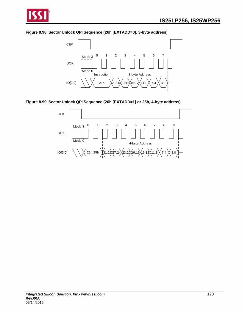
IS25LP256, IS25WP256
Integrated Silicon Solution, Inc.- www.issi.com 128 Rev.00A 05/14/2015
Figure 8.98 Sector Unlock QPI Sequence (26h [EXTADD=0], 3-byte address)
26h
CE#
SCK
IO[3:0]
3-byte Address
0 1 2 3 4 5 6 7Mode 3
Mode 0
23:20 19:16 15:12 11:8 7:4 3:0
Instruction
Figure 8.99 Sector Unlock QPI Sequence (26h [EXTADD=1] or 25h, 4-byte address)
26h/25h
CE#
SCK
IO[3:0]
4-byte Address
0 1 2 3 4 5 6 7Mode 3
Mode 0
23:20 19:16 15:12 11:8 7:4 3:031:28 27:24
8 9

IS25LP256, IS25WP256
Integrated Silicon Solution, Inc.- www.issi.com 129 Rev.00A 05/14/2015
SECTOR LOCK OPERATION (SECLOCK, 24h)
The Sector Lock command relocks a sector that was previously unlocked by the Sector Unlock command. The instruction code does not require an address to be specified, as only one sector can be enabled at a time. The remaining sectors within the same block remain in read-only mode. Figure 8.100 Sector Lock Sequence
Instruction = 24h
CE#
SCK
SI
0 1 2 3 4 5 6 7Mode 3
Mode 0
SO High Impedance
Figure 8.101 Sector Lock QPI Sequence
24h
CE#
SCK
IO[3:0]
0 1Mode 3
Mode 0
IS25LP256, IS25WP256
Integrated Silicon Solution, Inc.- www.issi.com 130 Rev.00A 05/14/2015
8.46 AUTOBOOT
SPI devices normally require 32 or more cycles of command and address shifting to initiate a read command. And, in order to read boot code from an SPI device, the host memory controller or processor must supply the read command from a hardwired state machine or from some host processor internal ROM code. Parallel NOR devices need only an initial address, supplied in parallel in a single cycle, and initial access time to start reading boot code. The AutoBoot feature allows the host memory controller to take boot code from the device immediately after the end of reset, without having to send a read command. This saves 32 or more cycles and simplifies the logic needed to initiate the reading of boot code. • As part of the Power-up Reset, Hardware Reset, or Software Reset process the AutoBoot feature
automatically starts a read access from a pre-specified address. At the time the reset process is completed, the device is ready to deliver code from the starting address. The host memory controller only needs to drive CE# signal from high to low and begin toggling the SCK signal. The device will delay code output for a pre-specified number of clock cycles before code streams out.
– The Auto Boot Start Delay (ABSD) field of the AutoBoot register specifies the initial delay if any is needed
by the host. – The host cannot send commands during this time. – If QE bit (Bit 6) in the Status Register is set to “1”, Quad IO Read operation will be selected. If it is set to
“0”, fast read SPI operation will be applied. Maximum operation frequency will be 166MHz for both operations.
• The starting address of the boot code is selected by the value programmed into the AutoBoot Start Address
(ABSA) field of the AutoBoot Register.
– Data will continuously shift out until CE# returns high. • At any point after the first data byte is transferred, when CE# returns high, the SPI device will reset to
standard SPI mode; able to accept normal command operations.
– A minimum of one byte must be transferred. – AutoBoot mode will not initiate again until another power cycle or a reset occurs.
• An AutoBoot Enable bit (ABE) is set to enable the AutoBoot feature. The AutoBoot register bits are non-volatile and provide: • The starting address set by the AutoBoot Start Address (ABSA). • The number of initial delay cycles, set by the AutoBoot Start Delay (ABSD) 4-bit count value.

IS25LP256, IS25WP256
Integrated Silicon Solution, Inc.- www.issi.com 131 Rev.00A 05/14/2015
Figure 8.102 AutoBoot Sequence (QE = 0)
7
CE#
SCK
SI
3 2SO 1 0
Data Out 1High Impedance
6 5 4
0 1 2 ... n-1 n n+1 n+2 n+3 n+4 n+5 n+6 n+7 n+8 n+9 n+10Mode 3
Mode 0
tVABSD Delay (n)
7 6 ...
Data Out 2 ...
...
Figure 8.103 AutoBoot Sequence (QE = 1)
4
CE#
SCK
4 0 4 0
High Impedance
0 4 0
Mode 3
Mode 0
IO0
IO1
IO2
IO3
5 1
Data Out 1
5 1 5 1 5 1
7 3
6 2
7 3 7 3
6 2 6 2
7 3
6 2
Data Out 2 Data Out 3 Data Out 4
tVABSD Delay (n)
0 1 2 ... n-1 n n+1 n+2 n+3 n+4 n+5 n+6 n+7 n+8 n+9 n+10 ...
4 0
5 1 ...
7 3 ...
6 2 ...
Data Out 5
...
...

IS25LP256, IS25WP256
Integrated Silicon Solution, Inc.- www.issi.com 132 Rev.00A 05/14/2015
AUTOBOOT REGISTER READ OPERATION (RDABR, 14h)
The AutoBoot Register Read command is shifted in. Then the 32bit AutoBoot Register is shifted out, least significant byte first, most significant bit of each byte first. It is possible to read the AutoBoot Register continuously by providing multiples of 32bits. Figure 8.104 RDABR Sequence (QE = 1)
Instruction = 14h
7
CE#
SCK
SI
3 2SO 1 0
Data Out 1
6 5
0 1 2 3 4 5 6 7 8 9 10 11 12 13 14 15Mode 3
Mode 0
4
tV
...
...
Figure 8.105 RDABR QPI Sequence (QE = 1)
14h
0 1Mode 3
Mode 0
2 3
7:4 3:0
CE#
SCK
IO[3:0]
tV
Data Out
...
...
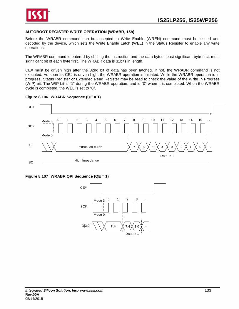
IS25LP256, IS25WP256
Integrated Silicon Solution, Inc.- www.issi.com 133 Rev.00A 05/14/2015
AUTOBOOT REGISTER WRITE OPERATION (WRABR, 15h)
Before the WRABR command can be accepted, a Write Enable (WREN) command must be issued and decoded by the device, which sets the Write Enable Latch (WEL) in the Status Register to enable any write operations. The WRABR command is entered by shifting the instruction and the data bytes, least significant byte first, most significant bit of each byte first. The WRABR data is 32bits in length. CE# must be driven high after the 32nd bit of data has been latched. If not, the WRABR command is not executed. As soon as CE# is driven high, the WRABR operation is initiated. While the WRABR operation is in progress, Status Register or Extended Read Register may be read to check the value of the Write In Progress (WIP) bit. The WIP bit is “1” during the WRABR operation, and is “0” when it is completed. When the WRABR cycle is completed, the WEL is set to “0”. Figure 8.106 WRABR Sequence (QE = 1)
Instruction = 15h 7
CE#
SCK
SI3 2
SO
1 0
Data In 1
6 5
0 1 2 3 4 5 6 7 8 9 10 11 12 13 14 15Mode 3
Mode 0
4
High Impedance
...
...
Figure 8.107 WRABR QPI Sequence (QE = 1)
15h
0 1Mode 3
Mode 0
2 3
7:4 3:0
CE#
SCK
IO[3:0]
Data In 1
...
...
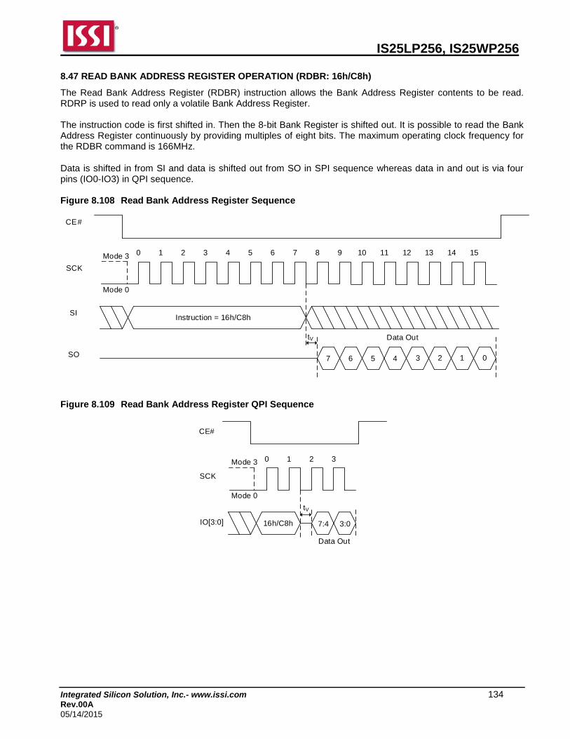
IS25LP256, IS25WP256
Integrated Silicon Solution, Inc.- www.issi.com 134 Rev.00A 05/14/2015
8.47 READ BANK ADDRESS REGISTER OPERATION (RDBR: 16h/C8h)
The Read Bank Address Register (RDBR) instruction allows the Bank Address Register contents to be read. RDRP is used to read only a volatile Bank Address Register. The instruction code is first shifted in. Then the 8-bit Bank Register is shifted out. It is possible to read the Bank Address Register continuously by providing multiples of eight bits. The maximum operating clock frequency for the RDBR command is 166MHz. Data is shifted in from SI and data is shifted out from SO in SPI sequence whereas data in and out is via four pins (IO0-IO3) in QPI sequence. Figure 8.108 Read Bank Address Register Sequence
Instruction = 16h/C8h
7
CE#
SCK
SI
3 2SO 1 0
Data Out
6 5
0 1 2 3 4 5 6 7 8 9 10 11 12 13 14 15Mode 3
Mode 0
4
tV
Figure 8.109 Read Bank Address Register QPI Sequence
16h/C8h
0 1Mode 3
Mode 0
2 3
7:4 3:0
CE#
SCK
IO[3:0]
tV
Data Out
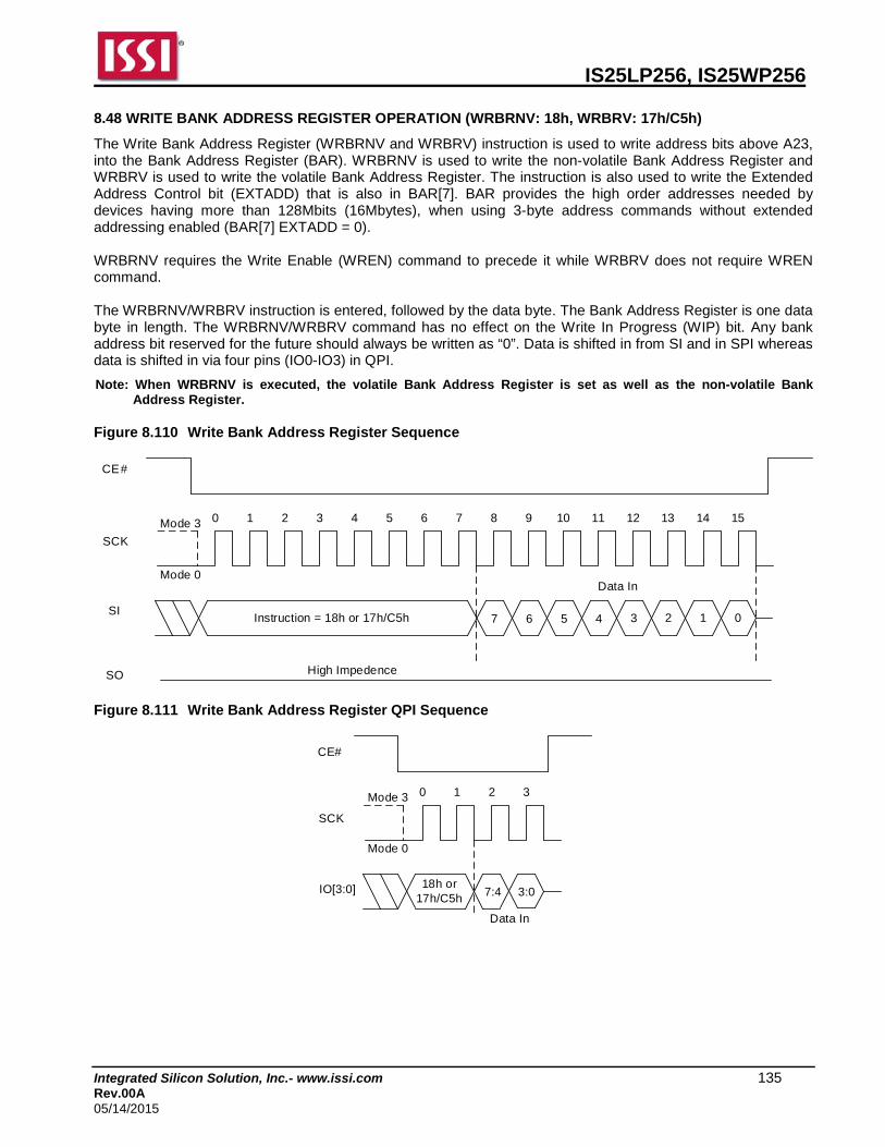
IS25LP256, IS25WP256
Integrated Silicon Solution, Inc.- www.issi.com 135 Rev.00A 05/14/2015
8.48 WRITE BANK ADDRESS REGISTER OPERATION (WRBRNV: 18h, WRBRV: 17h/C5h)
The Write Bank Address Register (WRBRNV and WRBRV) instruction is used to write address bits above A23, into the Bank Address Register (BAR). WRBRNV is used to write the non-volatile Bank Address Register and WRBRV is used to write the volatile Bank Address Register. The instruction is also used to write the Extended Address Control bit (EXTADD) that is also in BAR[7]. BAR provides the high order addresses needed by devices having more than 128Mbits (16Mbytes), when using 3-byte address commands without extended addressing enabled (BAR[7] EXTADD = 0). WRBRNV requires the Write Enable (WREN) command to precede it while WRBRV does not require WREN command. The WRBRNV/WRBRV instruction is entered, followed by the data byte. The Bank Address Register is one data byte in length. The WRBRNV/WRBRV command has no effect on the Write In Progress (WIP) bit. Any bank address bit reserved for the future should always be written as “0”. Data is shifted in from SI and in SPI whereas data is shifted in via four pins (IO0-IO3) in QPI.
Note: When WRBRNV is executed, the volatile Bank Address Register is set as well as the non-volatile Bank Address Register.
Figure 8.110 Write Bank Address Register Sequence
Instruction = 18h or 17h/C5h
CE#
SCK
SI
SO
Data In
0 1 2 3 4 5 6 7 8 9 10 11 12 13 14 15Mode 3
Mode 0
7 3 2 1 06 5 4
High Impedence
Figure 8.111 Write Bank Address Register QPI Sequence
18h or17h/C5h
0 1Mode 3
Mode 0
2 3
7:4 3:0
CE#
SCK
IO[3:0]
Data In
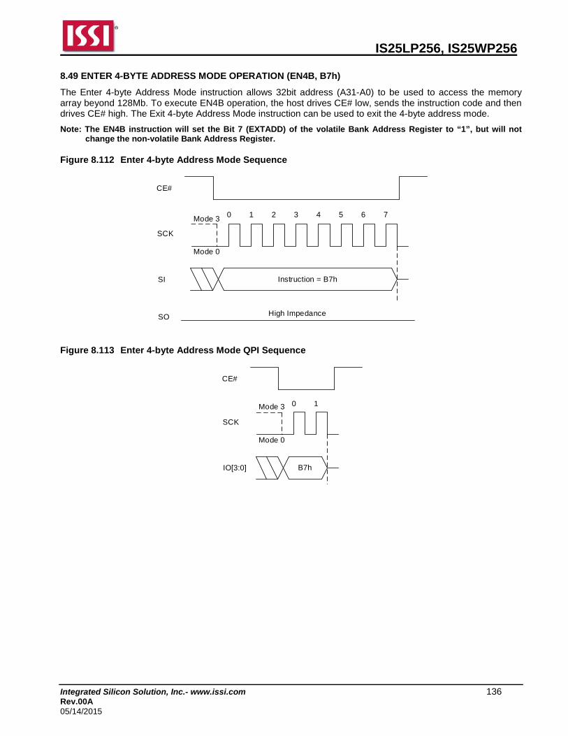
IS25LP256, IS25WP256
Integrated Silicon Solution, Inc.- www.issi.com 136 Rev.00A 05/14/2015
8.49 ENTER 4-BYTE ADDRESS MODE OPERATION (EN4B, B7h)
The Enter 4-byte Address Mode instruction allows 32bit address (A31-A0) to be used to access the memory array beyond 128Mb. To execute EN4B operation, the host drives CE# low, sends the instruction code and then drives CE# high. The Exit 4-byte Address Mode instruction can be used to exit the 4-byte address mode.
Note: The EN4B instruction will set the Bit 7 (EXTADD) of the volatile Bank Address Register to “1”, but will not change the non-volatile Bank Address Register.
Figure 8.112 Enter 4-byte Address Mode Sequence
Instruction = B7h
CE#
SCK
SI
0 1 2 3 4 5 6 7Mode 3
Mode 0
SO High Impedance
Figure 8.113 Enter 4-byte Address Mode QPI Sequence
B7h
CE#
SCK
IO[3:0]
0 1Mode 3
Mode 0
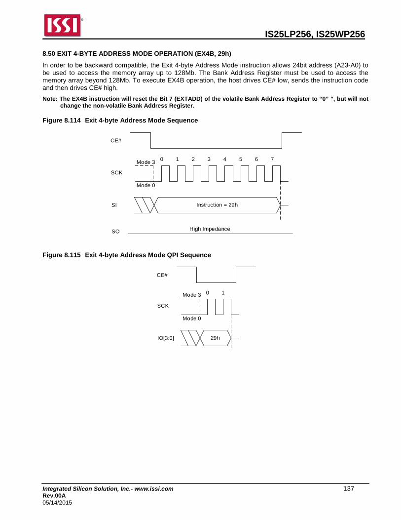
IS25LP256, IS25WP256
Integrated Silicon Solution, Inc.- www.issi.com 137 Rev.00A 05/14/2015
8.50 EXIT 4-BYTE ADDRESS MODE OPERATION (EX4B, 29h)
In order to be backward compatible, the Exit 4-byte Address Mode instruction allows 24bit address (A23-A0) to be used to access the memory array up to 128Mb. The Bank Address Register must be used to access the memory array beyond 128Mb. To execute EX4B operation, the host drives CE# low, sends the instruction code and then drives CE# high.
Note: The EX4B instruction will reset the Bit 7 (EXTADD) of the volatile Bank Address Register to “0” ”, but will not change the non-volatile Bank Address Register.
Figure 8.114 Exit 4-byte Address Mode Sequence
Instruction = 29h
CE#
SCK
SI
0 1 2 3 4 5 6 7Mode 3
Mode 0
SO High Impedance
Figure 8.115 Exit 4-byte Address Mode QPI Sequence
29h
CE#
SCK
IO[3:0]
0 1Mode 3
Mode 0

IS25LP256, IS25WP256
Integrated Silicon Solution, Inc.- www.issi.com 138 Rev.00A 05/14/2015
8.51 READ DYB OPERATION (RDDYB, FAh or 4RDDYB, E0h)
FAh (EXTADD=0) is followed by a 3-byte address (A23-A0) or • FAh (EXTADD=1) is followed by a 4-byte address (A31-A0) or • E0h is followed by a 4-byte address (A31-A0) The instruction is used to read Dynamic Protection Bit (DYB) status of the given sector/block. The instruction code is entered first, followed by the 24-bit or 32-bit address selecting location zero within the desired sector/block as above. Then the 8-bit DYB access register contents are shifted out. Each bit (SPI) or four bits (QPI) are shifted out at the SCK frequency by the falling edge of the SCK signal. It is possible to read the same DYB access register continuously by providing multiples of eight bits. The address of the DYB register does not increment so this is not a means to read the entire DYB array. Each location must be read with a separate Read DYB instruction. The maximum operating clock frequency for READ command is 166MHz.
Note: The high order address bits not used by 256M must be zero. Figure 8.116 Read DYB Sequence (FAh [EXTADD=0], 3-byte address)
Instruction = FAh
CE#
SCK
SI
SO
0 1 ... 7 8 9 ... 31 32 33 34 35 36 37 38 39Mode 3
Mode 0
3-byte Address
tV
7 3 2 1 06 5 4
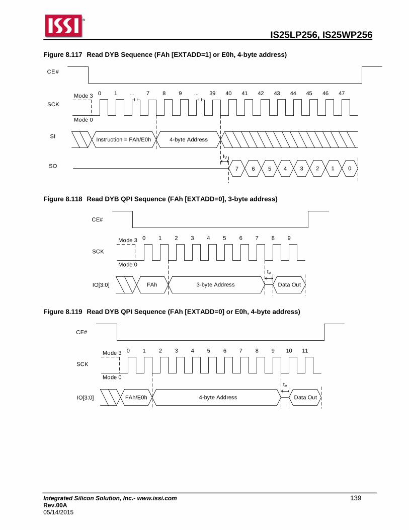
IS25LP256, IS25WP256
Integrated Silicon Solution, Inc.- www.issi.com 139 Rev.00A 05/14/2015
Figure 8.117 Read DYB Sequence (FAh [EXTADD=1] or E0h, 4-byte address)
Instruction = FAh/E0h
CE#
SCK
SI
SO
0 1 ... 7 8 9 ... 39 40 41 42 43 44 45 46 47Mode 3
Mode 0
4-byte Address
tV
7 3 2 1 06 5 4
Figure 8.118 Read DYB QPI Sequence (FAh [EXTADD=0], 3-byte address)
FAh
CE#
SCK
IO[3:0]
0 1Mode 3
Mode 0
2 3 4 5 6 7 8 9
3-byte Address Data Out
tV
Figure 8.119 Read DYB QPI Sequence (FAh [EXTADD=0] or E0h, 4-byte address)
FAh/E0h
CE#
SCK
IO[3:0]
0 1Mode 3
Mode 0
2 3 4 5 6 7 10 11
4-byte Address Data Out
tV
8 9
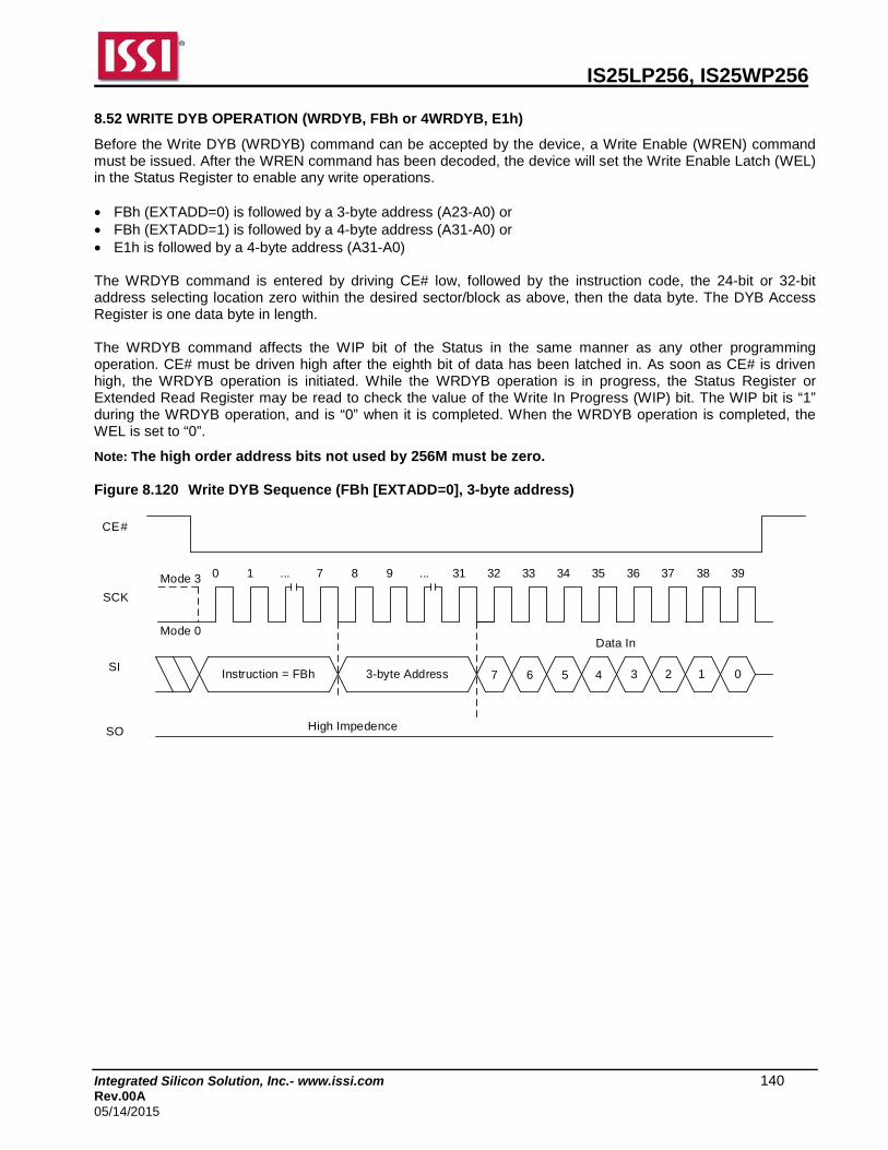
IS25LP256, IS25WP256
Integrated Silicon Solution, Inc.- www.issi.com 140 Rev.00A 05/14/2015
8.52 WRITE DYB OPERATION (WRDYB, FBh or 4WRDYB, E1h)
Before the Write DYB (WRDYB) command can be accepted by the device, a Write Enable (WREN) command must be issued. After the WREN command has been decoded, the device will set the Write Enable Latch (WEL) in the Status Register to enable any write operations. • FBh (EXTADD=0) is followed by a 3-byte address (A23-A0) or • FBh (EXTADD=1) is followed by a 4-byte address (A31-A0) or • E1h is followed by a 4-byte address (A31-A0) The WRDYB command is entered by driving CE# low, followed by the instruction code, the 24-bit or 32-bit address selecting location zero within the desired sector/block as above, then the data byte. The DYB Access Register is one data byte in length. The WRDYB command affects the WIP bit of the Status in the same manner as any other programming operation. CE# must be driven high after the eighth bit of data has been latched in. As soon as CE# is driven high, the WRDYB operation is initiated. While the WRDYB operation is in progress, the Status Register or Extended Read Register may be read to check the value of the Write In Progress (WIP) bit. The WIP bit is “1” during the WRDYB operation, and is “0” when it is completed. When the WRDYB operation is completed, the WEL is set to “0”.
Note: The high order address bits not used by 256M must be zero. Figure 8.120 Write DYB Sequence (FBh [EXTADD=0], 3-byte address)
Instruction = FBh
CE#
SCK
SI
SO
0 1 ... 7 8 9 ... 31 32 33 34 35 36 37 38 39Mode 3
Mode 0
3-byte Address
Data In
High Impedence
7 3 2 1 06 5 4
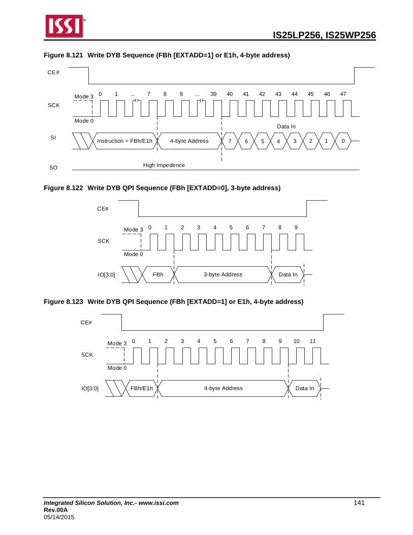
IS25LP256, IS25WP256
Integrated Silicon Solution, Inc.- www.issi.com 141 Rev.00A 05/14/2015
Figure 8.121 Write DYB Sequence (FBh [EXTADD=1] or E1h, 4-byte address)
Instruction = FBh/E1h
CE#
SCK
SI
SO
0 1 ... 7 8 9 ... 39 40 41 42 43 44 45 46 47Mode 3
Mode 0
4-byte Address
Data In
High Impedence
7 3 2 1 06 5 4
Figure 8.122 Write DYB QPI Sequence (FBh [EXTADD=0], 3-byte address)
FBh
CE#
SCK
IO[3:0]
0 1Mode 3
Mode 0
2 3 4 5 6 7 8 9
3-byte Address Data In
Figure 8.123 Write DYB QPI Sequence (FBh [EXTADD=1] or E1h, 4-byte address)
FBh/E1h
CE#
SCK
IO[3:0]
0 1Mode 3
Mode 0
2 3 4 5 6 7 10 11
4-byte Address Data In
8 9
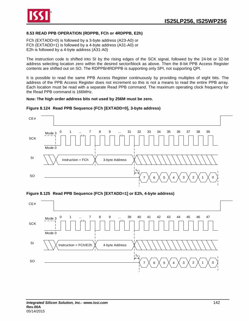
IS25LP256, IS25WP256
Integrated Silicon Solution, Inc.- www.issi.com 142 Rev.00A 05/14/2015
8.53 READ PPB OPERATION (RDPPB, FCh or 4RDPPB, E2h)
FCh (EXTADD=0) is followed by a 3-byte address (A23-A0) or FCh (EXTADD=1) is followed by a 4-byte address (A31-A0) or E2h is followed by a 4-byte address (A31-A0) The instruction code is shifted into SI by the rising edges of the SCK signal, followed by the 24-bit or 32-bit address selecting location zero within the desired sector/block as above. Then the 8-bit PPB Access Register contents are shifted out on SO. The RDPPB/4RDPPB is supporting only SPI, not supporting QPI. It is possible to read the same PPB Access Register continuously by providing multiples of eight bits. The address of the PPB Access Register does not increment so this is not a means to read the entire PPB array. Each location must be read with a separate Read PPB command. The maximum operating clock frequency for the Read PPB command is 166MHz.
Note: The high order address bits not used by 256M must be zero. Figure 8.124 Read PPB Sequence (FCh [EXTADD=0], 3-byte address)
Instruction = FCh
CE#
SCK
SI
SO
0 1 ... 7 8 9 ... 31 32 33 34 35 36 37 38 39Mode 3
Mode 0
3-byte Address
tV
7 3 2 1 06 5 4
Figure 8.125 Read PPB Sequence (FCh [EXTADD=1] or E2h, 4-byte address)
Instruction = FCh/E2h
CE#
SCK
SI
SO
0 1 ... 7 8 9 ... 39 40 41 42 43 44 45 46 47Mode 3
Mode 0
4-byte Address
tV
7 3 2 1 06 5 4

IS25LP256, IS25WP256
Integrated Silicon Solution, Inc.- www.issi.com 143 Rev.00A 05/14/2015
8.54 PROGRAM PPB OPERATION (PGPPB, FDh or 4PGPPB, E3h)
Before the Program PPB (PGPPB/4PGPPB) command is sent, a Write Enable (WREN) command must be issued. After the WREN command has been decoded, the device will set the Write Enable Latch (WEL) in the Status Register. FDh (EXTADD=0) is followed by a 3-byte address (A23-A0) or FDh (EXTADD=1) is followed by a 4-byte address (A31-A0) or E3h is followed by a 4-byte address (A31-A0) The PGPPB/4PGPPB command is entered by driving CE# low, followed by the instruction code, followed by the 24-bit or 32-bit address selecting location zero within the desired sector/block as above. The PGPPB/4PGPPB command affects the WIP bit in the same manner as any other programming operation. CE# must be driven high after the last bit of address has been latched in. As soon as CE# is driven high, the PGPPB/4PGPPB operation is initiated. While the PGPPB/4PGPPB operation is in progress, the Status Register or Extended Read Register may be read to check the value of the Write In Progress (WIP) bit. The WIP bit is “1” during the PGPPB/4PGPPB operation, and is “0” when it is completed. When the PGPPB/4PGPPB operation is completed, the WEL is set to “0”.
Note: The high order address bits not used by 256M must be zero. Figure 8.126 Program PPB Sequence (FDh [EXTADD=0], 3-byte address)
Instruction = FDh
CE#
SCK
SI
SO
0 1 ... 7 8 9 ... 31Mode 3
Mode 0
3-byte Address
High Impedence
Figure 8.127 Program PPB Sequence (FDh [EXTADD=1] or E3h, 4-byte address)
Instruction = FDh/E3h
CE#
SCK
SI
SO
0 1 ... 7 8 9 ... 39Mode 3
Mode 0
4-byte Address
High Impedence

IS25LP256, IS25WP256
Integrated Silicon Solution, Inc.- www.issi.com 144 Rev.00A 05/14/2015
Figure 8.128 Program PPB QPI Sequence (FDh [EXTADD=0], 3-byte address)
FDh
CE#
SCK
IO[3:0]
0 1Mode 3
Mode 0
2 3 4 5 6 7
3-byte Address
Figure 8.129 Program PPB QPI Sequence (FDh [EXTADD=1] or E3h, 4-byte address)
FDh/E3h
CE#
SCK
IO[3:0]
0 1Mode 3
Mode 0
2 3 4 5 6 7 8 9
4-byte Address
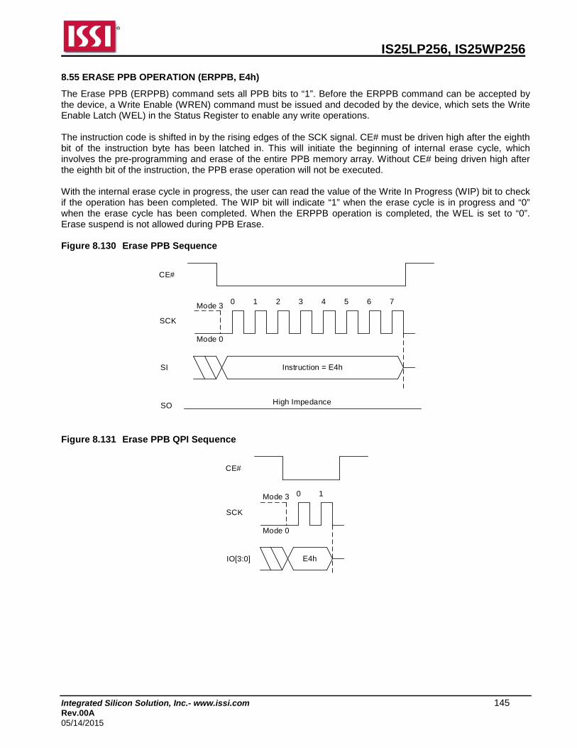
IS25LP256, IS25WP256
Integrated Silicon Solution, Inc.- www.issi.com 145 Rev.00A 05/14/2015
8.55 ERASE PPB OPERATION (ERPPB, E4h)
The Erase PPB (ERPPB) command sets all PPB bits to “1”. Before the ERPPB command can be accepted by the device, a Write Enable (WREN) command must be issued and decoded by the device, which sets the Write Enable Latch (WEL) in the Status Register to enable any write operations. The instruction code is shifted in by the rising edges of the SCK signal. CE# must be driven high after the eighth bit of the instruction byte has been latched in. This will initiate the beginning of internal erase cycle, which involves the pre-programming and erase of the entire PPB memory array. Without CE# being driven high after the eighth bit of the instruction, the PPB erase operation will not be executed. With the internal erase cycle in progress, the user can read the value of the Write In Progress (WIP) bit to check if the operation has been completed. The WIP bit will indicate “1” when the erase cycle is in progress and “0” when the erase cycle has been completed. When the ERPPB operation is completed, the WEL is set to “0”. Erase suspend is not allowed during PPB Erase. Figure 8.130 Erase PPB Sequence
Instruction = E4h
CE#
SCK
SI
0 1 2 3 4 5 6 7Mode 3
Mode 0
SO High Impedance
Figure 8.131 Erase PPB QPI Sequence
E4h
CE#
SCK
IO[3:0]
0 1Mode 3
Mode 0

IS25LP256, IS25WP256
Integrated Silicon Solution, Inc.- www.issi.com 146 Rev.00A 05/14/2015
8.56 READ ASP OPERATION (RDASP, 2Bh)
The RDASP instruction code is shifted in by the rising edge of the SCK signal. Then the 16-bit ASP register contents is shifted out, least significant byte first, most significant bit of each byte first. Each bit is shifted out at the SCK frequency by the falling edge of the SCK signal. It is possible to read the ASP register continuously by providing multiples of 16 bits. The maximum operating clock frequency for the RDASP command is 166MHz. Figure 8.132 Read ASP Sequence
8 9 ... 15 16 17 ... 23
Instruction = 2Bh
CE#
SCK
SI
SO
0 1 2 3 4 5 6 7Mode 3
Mode 0
tV
7 15 14 86 ... 0 ...
1st byte Data Out 2nd byte Data Out
Figure 8.133 Read ASP QPI Sequence
2Bh
CE#
SCK
IO[3:0]
0 1Mode 3
Mode 0
2 3 4 5
1st byteData Out
tV
2nd byte Data Out
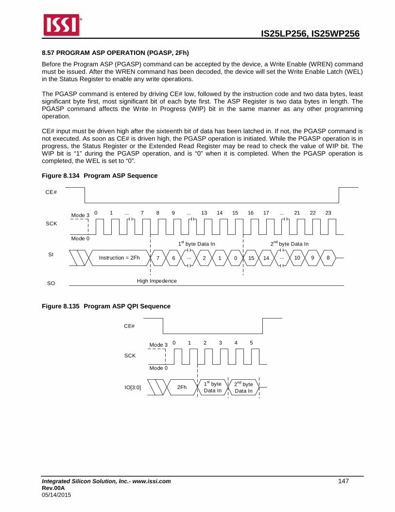
IS25LP256, IS25WP256
Integrated Silicon Solution, Inc.- www.issi.com 147 Rev.00A 05/14/2015
8.57 PROGRAM ASP OPERATION (PGASP, 2Fh)
Before the Program ASP (PGASP) command can be accepted by the device, a Write Enable (WREN) command must be issued. After the WREN command has been decoded, the device will set the Write Enable Latch (WEL) in the Status Register to enable any write operations. The PGASP command is entered by driving CE# low, followed by the instruction code and two data bytes, least significant byte first, most significant bit of each byte first. The ASP Register is two data bytes in length. The PGASP command affects the Write In Progress (WIP) bit in the same manner as any other programming operation. CE# input must be driven high after the sixteenth bit of data has been latched in. If not, the PGASP command is not executed. As soon as CE# is driven high, the PGASP operation is initiated. While the PGASP operation is in progress, the Status Register or the Extended Read Register may be read to check the value of WIP bit. The WIP bit is “1” during the PGASP operation, and is “0” when it is completed. When the PGASP operation is completed, the WEL is set to “0”. Figure 8.134 Program ASP Sequence
Instruction = 2Fh
CE#
SCK
SI
SO
0 1 ... 7 8 9 ... 13 14 15 16 17 ... 21 22 23Mode 3
Mode 01st byte Data In
High Impedence
1 ... 10 9 80 15 147 6 ... 2
2nd byte Data In
Figure 8.135 Program ASP QPI Sequence
2Fh
SCK
IO[3:0]
0 1Mode 3
Mode 0
2 3 4 5
1st byteData In
2nd byte Data In
CE#
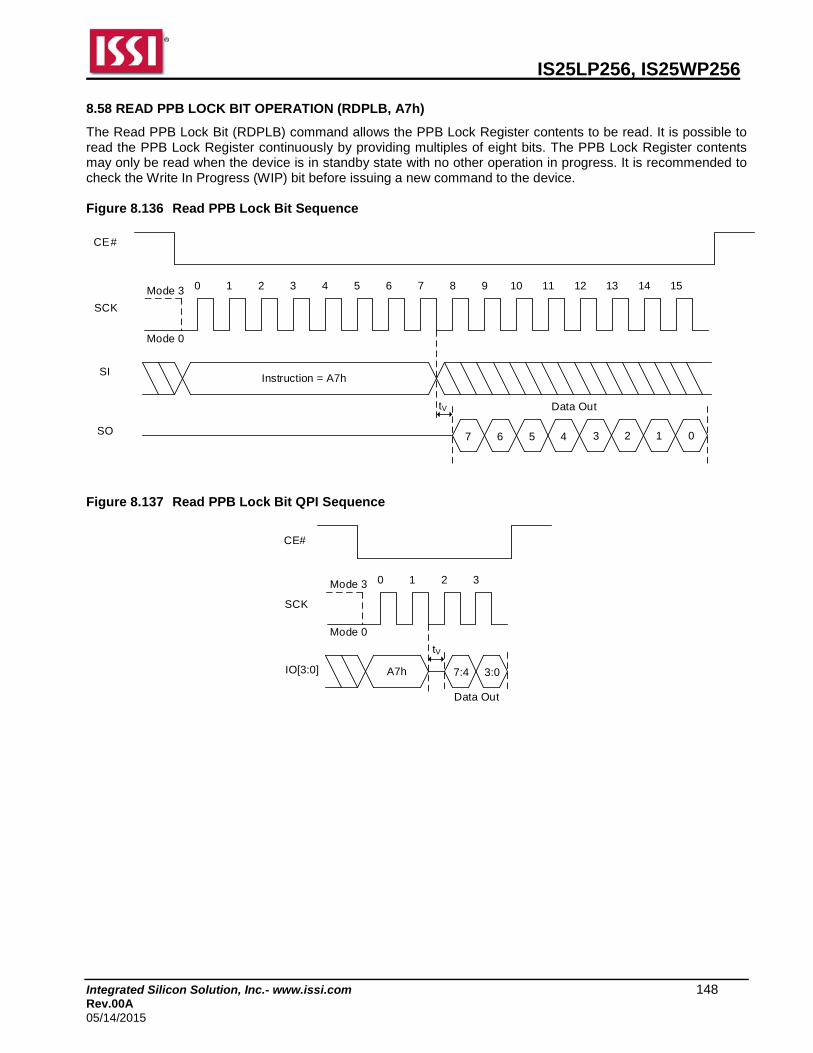
IS25LP256, IS25WP256
Integrated Silicon Solution, Inc.- www.issi.com 148 Rev.00A 05/14/2015
8.58 READ PPB LOCK BIT OPERATION (RDPLB, A7h)
The Read PPB Lock Bit (RDPLB) command allows the PPB Lock Register contents to be read. It is possible to read the PPB Lock Register continuously by providing multiples of eight bits. The PPB Lock Register contents may only be read when the device is in standby state with no other operation in progress. It is recommended to check the Write In Progress (WIP) bit before issuing a new command to the device. Figure 8.136 Read PPB Lock Bit Sequence
Instruction = A7h
7
CE#
SCK
SI
3 2SO 1 0
Data Out
6 5
0 1 2 3 4 5 6 7 8 9 10 11 12 13 14 15Mode 3
Mode 0
4
tV
Figure 8.137 Read PPB Lock Bit QPI Sequence
A7h
0 1Mode 3
Mode 0
2 3
7:4 3:0
CE#
SCK
IO[3:0]
tV
Data Out
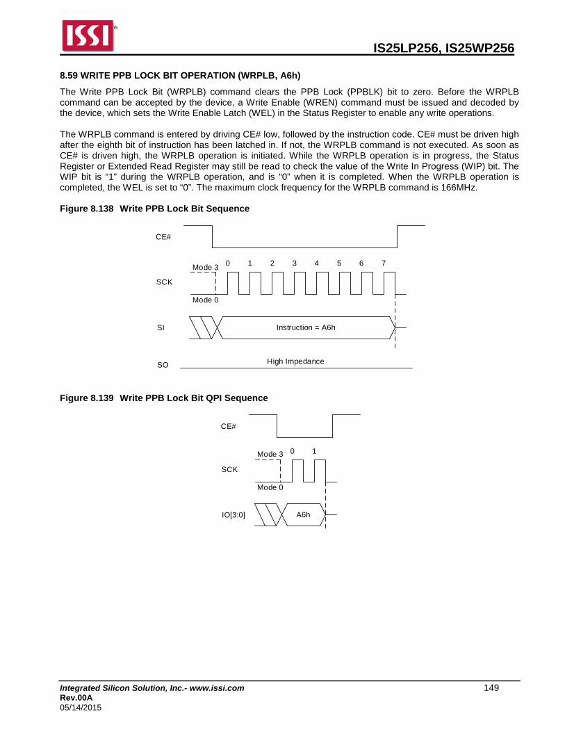
IS25LP256, IS25WP256
Integrated Silicon Solution, Inc.- www.issi.com 149 Rev.00A 05/14/2015
8.59 WRITE PPB LOCK BIT OPERATION (WRPLB, A6h)
The Write PPB Lock Bit (WRPLB) command clears the PPB Lock (PPBLK) bit to zero. Before the WRPLB command can be accepted by the device, a Write Enable (WREN) command must be issued and decoded by the device, which sets the Write Enable Latch (WEL) in the Status Register to enable any write operations. The WRPLB command is entered by driving CE# low, followed by the instruction code. CE# must be driven high after the eighth bit of instruction has been latched in. If not, the WRPLB command is not executed. As soon as CE# is driven high, the WRPLB operation is initiated. While the WRPLB operation is in progress, the Status Register or Extended Read Register may still be read to check the value of the Write In Progress (WIP) bit. The WIP bit is “1” during the WRPLB operation, and is “0” when it is completed. When the WRPLB operation is completed, the WEL is set to “0”. The maximum clock frequency for the WRPLB command is 166MHz. Figure 8.138 Write PPB Lock Bit Sequence
Instruction = A6h
CE#
SCK
SI
0 1 2 3 4 5 6 7Mode 3
Mode 0
SO High Impedance
Figure 8.139 Write PPB Lock Bit QPI Sequence
A6h
CE#
SCK
IO[3:0]
0 1Mode 3
Mode 0

IS25LP256, IS25WP256
Integrated Silicon Solution, Inc.- www.issi.com 150 Rev.00A 05/14/2015
8.60 SET FREEZE BIT OPERATION (SFRZ, 91h)
The Set FREEZE Bit (SFRZ) command sets FREEZE (PPB Lock Register bit7) to one. Please refer to the section 6.6.3 PPB Lock Register for more detail. Before the SFRZ command can be accepted by the device, a Write Enable (WREN) command must be issued and decoded by the device, which sets the Write Enable Latch (WEL) in the Status Register to enable any write operations. The SFRZ command is entered by driving CE# low, followed by the instruction code. CE# must be driven high after the eighth bit of instruction has been latched in. If not, the SFRZ command is not executed. As soon as CE# is driven high, the SFRZ operation is initiated. While the SFRZ operation is in progress, the Status Register or Extended Read Register may still be read to check the value of the Write In Progress (WIP) bit. The WIP bit is “1” during the SFRZ operation, and is “0” when it is completed. When the SFRZ operation is completed, the WEL is set to “0”. The maximum clock frequency for the SFRZ command is 166MHz. Figure 8.140 Set FREEZE Bit Sequence
Instruction = A6h
CE#
SCK
SI
0 1 2 3 4 5 6 7Mode 3
Mode 0
SO High Impedance
Figure 8.141 Set FREEZE Bit QPI Sequence
A6h
CE#
SCK
IO[3:0]
0 1Mode 3
Mode 0
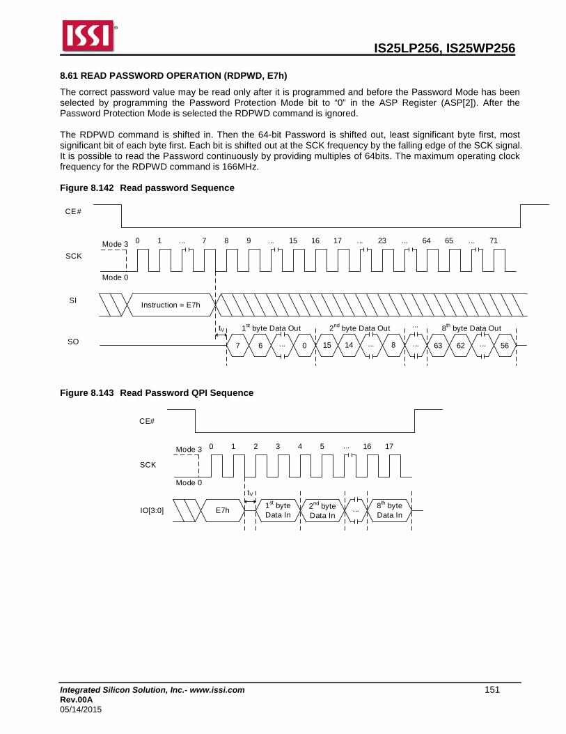
IS25LP256, IS25WP256
Integrated Silicon Solution, Inc.- www.issi.com 151 Rev.00A 05/14/2015
8.61 READ PASSWORD OPERATION (RDPWD, E7h)
The correct password value may be read only after it is programmed and before the Password Mode has been selected by programming the Password Protection Mode bit to “0” in the ASP Register (ASP[2]). After the Password Protection Mode is selected the RDPWD command is ignored. The RDPWD command is shifted in. Then the 64-bit Password is shifted out, least significant byte first, most significant bit of each byte first. Each bit is shifted out at the SCK frequency by the falling edge of the SCK signal. It is possible to read the Password continuously by providing multiples of 64bits. The maximum operating clock frequency for the RDPWD command is 166MHz. Figure 8.142 Read password Sequence
Instruction = E7h
CE#
SCK
SI
SO
0 1 ... 7 8 9 ... 15 16 17 ... 23 ... 64 65 ...Mode 3
Mode 0
tV
7 15 14 86 ... 0 63 62 56... ... ...
71
1st byte Data Out 2nd byte Data Out ... 8th byte Data Out
Figure 8.143 Read Password QPI Sequence
E7h
CE#
SCK
IO[3:0]
0 1Mode 3
Mode 0
2 3 4 5
tV
... 16 17
1st byteData In
2nd byte Data In
... 8th byte Data In

IS25LP256, IS25WP256
Integrated Silicon Solution, Inc.- www.issi.com 152 Rev.00A 05/14/2015
8.62 PROGRAM PASSWORD OPERATION (PGPWD, E8h)
Before the Program Password (PGPWD) command can be accepted by the device, a Write Enable (WREN) command must be issued and decoded by the device which sets the Write Enable Latch (WEL) to enable the PGPWD operation. The password can only be programmed before the Password Mode is selected by programming the Password Protection Mode bit to “0” in the ASP Register (ASP[2]). After the Password Protection Mode is selected the PGPWD command is ignored. The PGPWD command is entered by driving CE# low, followed by the instruction code and the password data bytes, least significant byte first, most significant bit of each byte first. The password is 64bits in length. CE# must be driven high after the 64th bit of data has been latched. If not, the PGPWD command is not executed. As soon as CE# is driven high, the PGPWD operation is initiated. While the PGPWD operation is in progress, the Status Register or Extended Read Register may be read to check the value of the Write In Progress (WIP) bit. The WIP bit is “1” during the PGPWD operation, and is “0” when it is completed. When the PGPWD operation is completed, the Write Enable Latch (WEL) is set to “0”. The maximum clock frequency for the PGPWD command is 166MHz. Figure 8.144 Program Password Sequence
Instruction = E8h
CE#
SCK
SI
SO
0 1 ... 7 8 9 ... 15 16 17 ... 23 ... 64 65 ...Mode 3
Mode 0
7 15 14 86 ... 0 63 62 56... ... ...
71
1st byte Data In 2nd byte Data In ... 8th byte Data In
High Impedence
Figure 8.145 Program Password QPI Sequence
E8h
CE#
SCK
IO[3:0]
0 1Mode 3
Mode 0
2 3 4 5
1st byteData In
2nd byte Data In
... 8th byte Data In
... 16 17
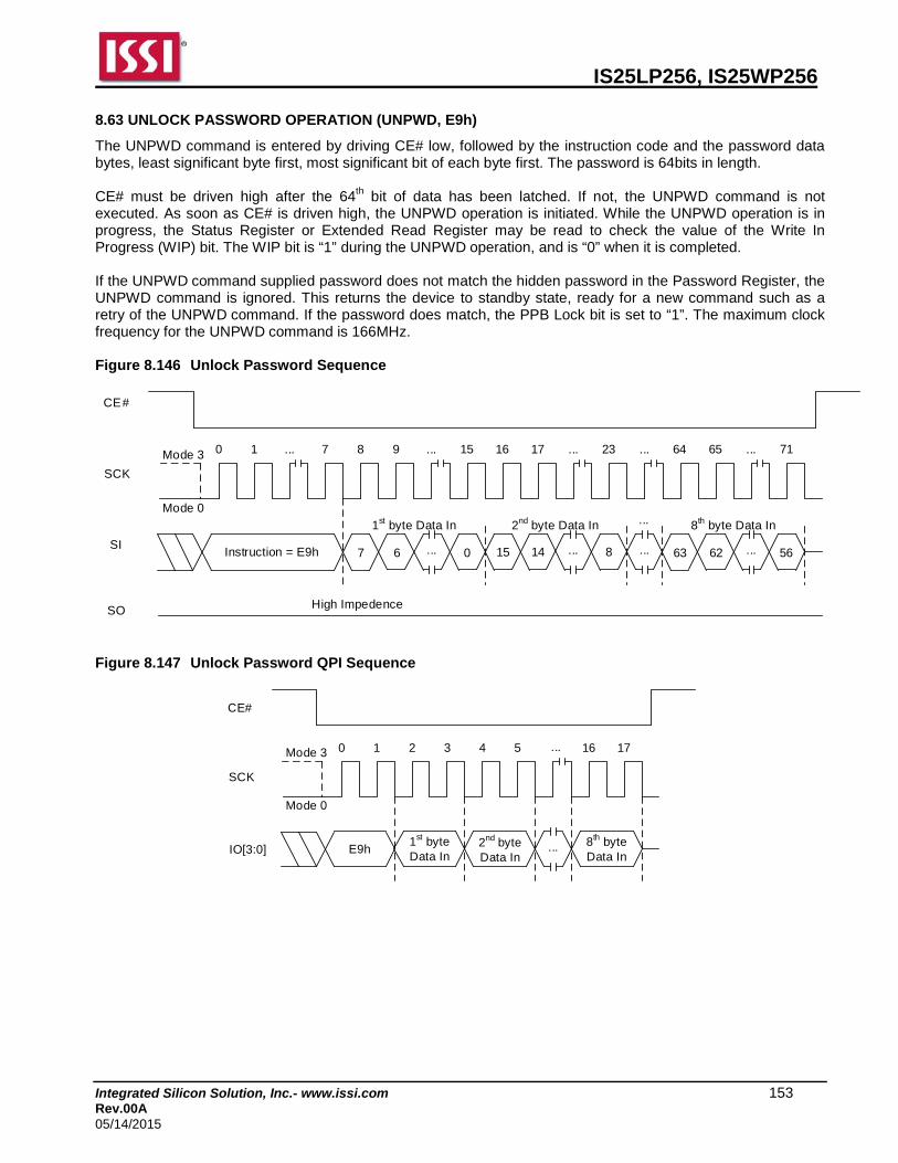
IS25LP256, IS25WP256
Integrated Silicon Solution, Inc.- www.issi.com 153 Rev.00A 05/14/2015
8.63 UNLOCK PASSWORD OPERATION (UNPWD, E9h)
The UNPWD command is entered by driving CE# low, followed by the instruction code and the password data bytes, least significant byte first, most significant bit of each byte first. The password is 64bits in length. CE# must be driven high after the 64th bit of data has been latched. If not, the UNPWD command is not executed. As soon as CE# is driven high, the UNPWD operation is initiated. While the UNPWD operation is in progress, the Status Register or Extended Read Register may be read to check the value of the Write In Progress (WIP) bit. The WIP bit is “1” during the UNPWD operation, and is “0” when it is completed. If the UNPWD command supplied password does not match the hidden password in the Password Register, the UNPWD command is ignored. This returns the device to standby state, ready for a new command such as a retry of the UNPWD command. If the password does match, the PPB Lock bit is set to “1”. The maximum clock frequency for the UNPWD command is 166MHz. Figure 8.146 Unlock Password Sequence
Instruction = E9h
CE#
SCK
SI
SO
0 1 ... 7 8 9 ... 15 16 17 ... 23 ... 64 65 ...Mode 3
Mode 0
7 15 14 86 ... 0 63 62 56... ... ...
71
1st byte Data In 2nd byte Data In ... 8th byte Data In
High Impedence
Figure 8.147 Unlock Password QPI Sequence
E9h
CE#
SCK
IO[3:0]
0 1Mode 3
Mode 0
2 3 4 5
1st byteData In
2nd byte Data In
... 8th byte Data In
... 16 17
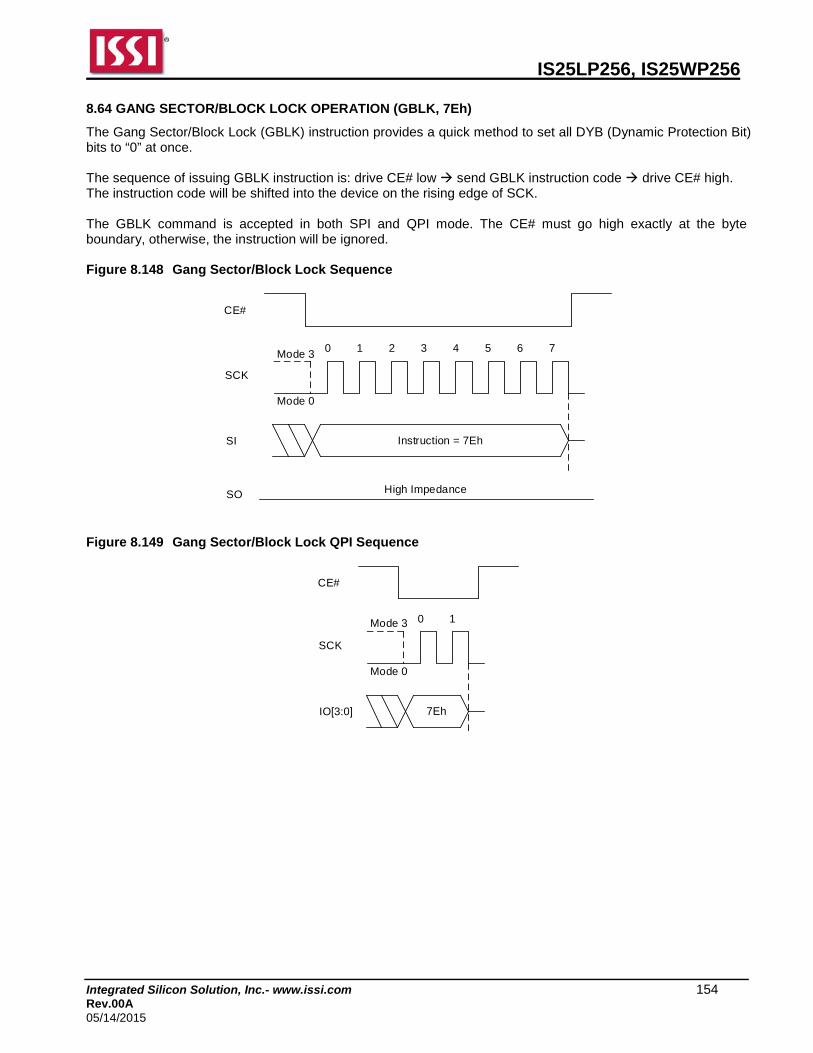
IS25LP256, IS25WP256
Integrated Silicon Solution, Inc.- www.issi.com 154 Rev.00A 05/14/2015
8.64 GANG SECTOR/BLOCK LOCK OPERATION (GBLK, 7Eh)
The Gang Sector/Block Lock (GBLK) instruction provides a quick method to set all DYB (Dynamic Protection Bit) bits to “0” at once. The sequence of issuing GBLK instruction is: drive CE# low send GBLK instruction code drive CE# high. The instruction code will be shifted into the device on the rising edge of SCK. The GBLK command is accepted in both SPI and QPI mode. The CE# must go high exactly at the byte boundary, otherwise, the instruction will be ignored. Figure 8.148 Gang Sector/Block Lock Sequence
Instruction = 7Eh
CE#
SCK
SI
0 1 2 3 4 5 6 7Mode 3
Mode 0
SO High Impedance
Figure 8.149 Gang Sector/Block Lock QPI Sequence
7Eh
CE#
SCK
IO[3:0]
0 1Mode 3
Mode 0
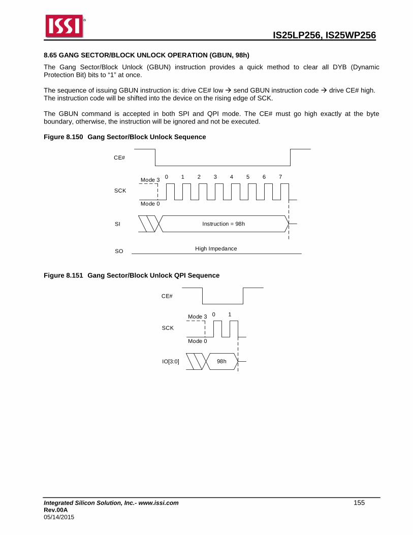
IS25LP256, IS25WP256
Integrated Silicon Solution, Inc.- www.issi.com 155 Rev.00A 05/14/2015
8.65 GANG SECTOR/BLOCK UNLOCK OPERATION (GBUN, 98h)
The Gang Sector/Block Unlock (GBUN) instruction provides a quick method to clear all DYB (Dynamic Protection Bit) bits to “1” at once. The sequence of issuing GBUN instruction is: drive CE# low send GBUN instruction code drive CE# high. The instruction code will be shifted into the device on the rising edge of SCK. The GBUN command is accepted in both SPI and QPI mode. The CE# must go high exactly at the byte boundary, otherwise, the instruction will be ignored and not be executed. Figure 8.150 Gang Sector/Block Unlock Sequence
Instruction = 98h
CE#
SCK
SI
0 1 2 3 4 5 6 7Mode 3
Mode 0
SO High Impedance
Figure 8.151 Gang Sector/Block Unlock QPI Sequence
98h
CE#
SCK
IO[3:0]
0 1Mode 3
Mode 0

IS25LP256, IS25WP256
Integrated Silicon Solution, Inc.- www.issi.com 156 Rev.00A 05/14/2015
9. ELECTRICAL CHARACTERISTICS
9.1 ABSOLUTE MAXIMUM RATINGS (1)
Storage Temperature -65°C to +150°C
Surface Mount Lead Soldering Temperature Standard Package 240°C 3 Seconds
Lead-free Package 260°C 3 Seconds
Input Voltage with Respect to Ground on All Pins -0.5V to VCC + 0.5V
All Output Voltage with Respect to Ground -0.5V to VCC + 0.5V
VCC IS25LP -0.5V to +6.0V
IS25WP -0.5V to +2.5V
Note: 1. Applied conditions greater than those listed in “Absolute Maximum Ratings” may cause permanent damage to
the device. This is a stress rating only and functional operation of the device at these or any other conditions above those indicated in the operational sections of this specification is not implied. Exposure to absolute maximum rating conditions for extended periods may affect reliability.
9.2 OPERATING RANGE
Operating Temperature
Extended Grade E -40°C to 105°C
Extended+ Grade E1 -40°C to 125°C
Automotive Grade A1 -40°C to 85°C
Automotive Grade A2 -40°C to 105°C
Automotive Grade A3 -40°C to 125°C
VCC Power Supply IS25LP 2.3V (VMIN) – 3.6V (VMAX); 3.3V (Typ)
IS25WP 1.65V (VMIN) –1.95V (VMAX); 1.8V (Typ)
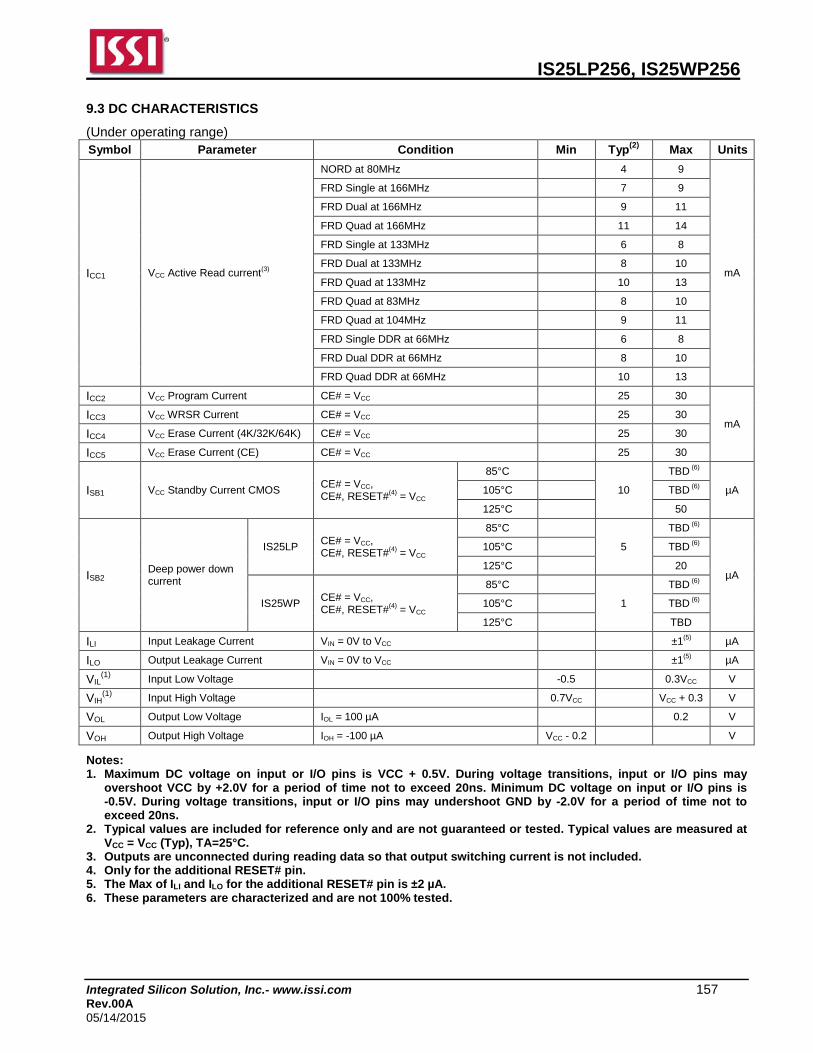
IS25LP256, IS25WP256
Integrated Silicon Solution, Inc.- www.issi.com 157 Rev.00A 05/14/2015
9.3 DC CHARACTERISTICS
(Under operating range) Symbol Parameter Condition Min Typ(2) Max Units
ICC1 VCC Active Read current(3)
NORD at 80MHz 4 9
mA
FRD Single at 166MHz 7 9
FRD Dual at 166MHz 9 11
FRD Quad at 166MHz 11 14
FRD Single at 133MHz 6 8
FRD Dual at 133MHz 8 10
FRD Quad at 133MHz 10 13
FRD Quad at 83MHz 8 10
FRD Quad at 104MHz 9 11
FRD Single DDR at 66MHz 6 8
FRD Dual DDR at 66MHz 8 10
FRD Quad DDR at 66MHz 10 13
ICC2 VCC Program Current CE# = VCC 25 30
mA ICC3 VCC WRSR Current CE# = VCC 25 30
ICC4 VCC Erase Current (4K/32K/64K) CE# = VCC 25 30
ICC5 VCC Erase Current (CE) CE# = VCC 25 30
ISB1 VCC Standby Current CMOS CE# = VCC, CE#, RESET#(4) = VCC
85°C
10
TBD (6)
µA 105°C TBD (6)
125°C 50
ISB2 Deep power down current
IS25LP CE# = VCC, CE#, RESET#(4) = VCC
85°C
5
TBD (6)
µA
105°C TBD (6)
125°C 20
IS25WP CE# = VCC, CE#, RESET#(4) = VCC
85°C
1
TBD (6)
105°C TBD (6)
125°C TBD
ILI Input Leakage Current VIN = 0V to VCC ±1(5) µA
ILO Output Leakage Current VIN = 0V to VCC ±1(5) µA
VIL(1) Input Low Voltage -0.5 0.3VCC V
VIH(1) Input High Voltage 0.7VCC VCC + 0.3 V
VOL Output Low Voltage IOL = 100 µA 0.2 V
VOH Output High Voltage IOH = -100 µA VCC - 0.2 V
Notes: 1. Maximum DC voltage on input or I/O pins is VCC + 0.5V. During voltage transitions, input or I/O pins may
overshoot VCC by +2.0V for a period of time not to exceed 20ns. Minimum DC voltage on input or I/O pins is -0.5V. During voltage transitions, input or I/O pins may undershoot GND by -2.0V for a period of time not to exceed 20ns.
2. Typical values are included for reference only and are not guaranteed or tested. Typical values are measured at VCC = VCC (Typ), TA=25°C.
3. Outputs are unconnected during reading data so that output switching current is not included. 4. Only for the additional RESET# pin. 5. The Max of ILI and ILO for the additional RESET# pin is ±2 µA. 6. These parameters are characterized and are not 100% tested.

IS25LP256, IS25WP256
Integrated Silicon Solution, Inc.- www.issi.com 158 Rev.00A 05/14/2015
9.4 AC MEASUREMENT CONDITIONS
Symbol Parameter Min Max Units
CL Load Capacitance up to 104MHz/52MHz DTR 30 pF
Load Capacitance up to 166MHz/80MHz DTR 15 pF
TR,TF Input Rise and Fall Times 5 ns
VIN Input Pulse Voltages 0.2VCC to 0.8VCC V
VREFI Input Timing Reference Voltages 0.3VCC to 0.7VCC V
VREFO Output Timing Reference Voltages 0.5VCC V
Figure 9.1 Output test load & AC measurement I/O Waveform
OUTPUT PIN
1.8k
1.2k 15/30pf
0.8VCC
0.2VCC
Input VCC/2AC
Measurement Level

IS25LP256, IS25WP256
Integrated Silicon Solution, Inc.- www.issi.com 159 Rev.00A 05/14/2015
9.5 AC CHARACTERISTICS
(Under operating range, refer to section 9.4 for AC measurement conditions) Symbol Parameter Min Typ(3) Max Units
fCT Clock Frequency for fast read mode: SPI, Dual, Dual I/O, Quad I/O, and QPI. 0 166 MHz
fC2, fT2, fQ2 Clock Frequency for fast read DTR: SPI DTR, Dual DTR, Dual I/O DTR, Quad I/O DTR, and QPI DTR.
0 80 MHz
fC Clock Frequency for read mode SPI 0 80 MHz
tCLCH(1) SCK Rise Time (peak to peak) 0.1 V/ns
tCHCL(1) SCK Fall Time ( peak to peak) 0.1 V/ns
tCKH SCK High Time For read mode 45% fC
ns For others 45% fCT/C2/T2/Q2
tCKL SCK Low Time For read mode 45% fC
ns For others 45% fCT/C2/T2/Q2
tCEH CE# High Time 7 ns
tCS CE# Setup Time 3 ns
tCH CE# Hold Time 3 ns
tDS Data In Setup Time Normal Mode 2
ns DTR Mode 1.5
tDH Data in Hold Time Normal Mode 2
ns DTR Mode 1.5
tV Output Valid
@ 166MHz (CL = 15pF) 7
ns @ 133MHz (CL = 15pF) 7
@ 104MHz (CL = 30pF) 8
tOH Output Hold Time 2 ns
tDIS(1) Output Disable Time 8 ns
tHLCH HOLD Active Setup Time relative to SCK 2 ns
tCHHH HOLD Active Hold Time relative to SCK 2 ns
tHHCH HOLD Not Active Setup Time relative to SCK 2 ns
tCHHL HOLD Not Active Hold Time relative to SCK 2 ns
tLZ(1) HOLD to Output Low Z 8 ns
tHZ(1) HOLD to Output High Z 8 ns
tEC
Sector Erase Time (4Kbyte) 50 300 ms
Block Erase Time (32Kbyte) 0.14 0.75 s
Block Erase time (64Kbyte) 0.2 1.0 s
Chip Erase Time 256Mb 50 180 s
tPP Page Program Time 0.2 0.8 ms

IS25LP256, IS25WP256
Integrated Silicon Solution, Inc.- www.issi.com 160 Rev.00A 05/14/2015
Symbol Parameter Min Typ(3) Max Units
tRES1(1) Release deep power down 15 µs
tDP(1) Deep power down 3 µs
tW Write Status Register time 2 15 ms
tSUS(1) Suspend to read ready 100 µs
tSRST(1) Software Reset recovery time 100 µs
tRESET(1) RESET# pin low pulse width 1(2) µs
tHWRST(1) Hardware Reset recovery time 100 µs
Notes: 1. These parameters are characterized and not 100% tested. 2. If the RESET# pulse is driven for a period shorter than 1µs (tRESET minimum), it may still reset the device,
however the 1µs minimum period is recommended to ensure reliable operation. 3. Typical values are included for reference only and are not guaranteed or tested. Typical values are measured at
VCC = VCC (Typ), TA=25°C.
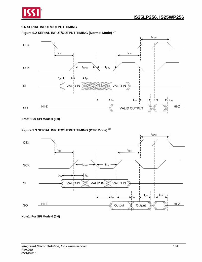
IS25LP256, IS25WP256
Integrated Silicon Solution, Inc.- www.issi.com 161 Rev.00A 05/14/2015
9.6 SERIAL INPUT/OUTPUT TIMING
Figure 9.2 SERIAL INPUT/OUTPUT TIMING (Normal Mode) (1)
HI-ZSO
SI
SCK
CE#
VALID IN
tCS
tCKH tCKL
tDS tDH
tCH
tCEH
tV tDIS
HI-Z
tOH
VALID IN
VALID OUTPUT
Note1: For SPI Mode 0 (0,0) Figure 9.3 SERIAL INPUT/OUTPUT TIMING (DTR Mode) (1)
HI-ZSO
SI
SCK
CE#
VALID IN
tCS
tCKH tCKL
tDS tDH
tCH
tCEH
tVtDIS
HI-Z
tOH
VALID INVALID IN
OutputOutput
tV
Note1: For SPI Mode 0 (0,0)

IS25LP256, IS25WP256
Integrated Silicon Solution, Inc.- www.issi.com 162 Rev.00A 05/14/2015
Figure 9.4 HOLD TIMING
SI
SO
SCK
CE#
HOLD#
tCHHL
tHLCH
tCHHH
tHHCH
tHZ tLZ

IS25LP256, IS25WP256
Integrated Silicon Solution, Inc.- www.issi.com 163 Rev.00A 05/14/2015
9.7 POWER-UP AND POWER-DOWN
At Power-up and Power-down, the device must be NOT SELECTED until Vcc reaches at the right level. (Adding a simple pull-up resistor on CE# is recommended.) Power up timing
VCC
VCC(max)
VCC(min)
V(write inhibit)
Reset StatetVCE
tPUW
Read Access Allowed Device fully accessible
Chip Selection Not Allowed
All Write Commands are Rejected
Symbol Parameter Min. Max Unit
tVCE(1) Vcc(min) to CE# Low 1 ms
tPUW(1) Power-up time delay to write instruction 1 10 ms
VWI(1) Write Inhibit Voltage
IS25LP 2.1 V
IS25WP 1.3
Note: These parameters are characterized and not 100% tested.
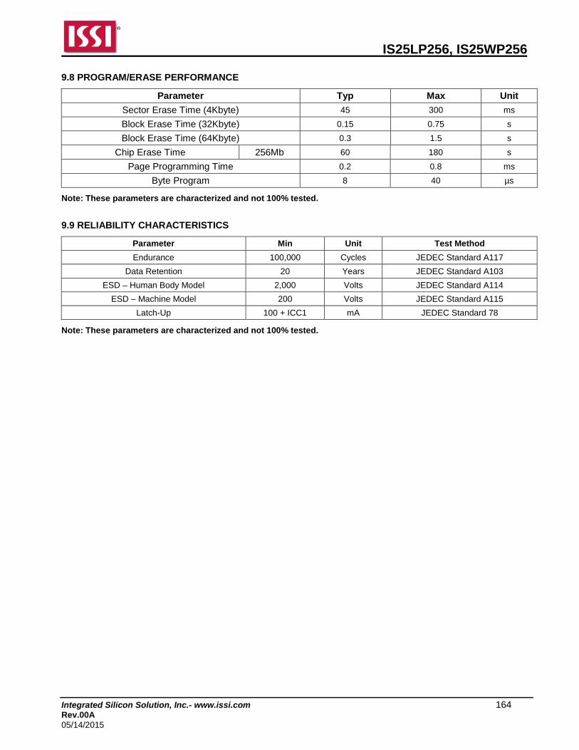
IS25LP256, IS25WP256
Integrated Silicon Solution, Inc.- www.issi.com 164 Rev.00A 05/14/2015
9.8 PROGRAM/ERASE PERFORMANCE
Parameter Typ Max Unit
Sector Erase Time (4Kbyte) 45 300 ms
Block Erase Time (32Kbyte) 0.15 0.75 s
Block Erase Time (64Kbyte) 0.3 1.5 s
Chip Erase Time 256Mb 60 180 s
Page Programming Time 0.2 0.8 ms
Byte Program 8 40 µs
Note: These parameters are characterized and not 100% tested.
9.9 RELIABILITY CHARACTERISTICS
Parameter Min Unit Test Method
Endurance 100,000 Cycles JEDEC Standard A117
Data Retention 20 Years JEDEC Standard A103
ESD – Human Body Model 2,000 Volts JEDEC Standard A114
ESD – Machine Model 200 Volts JEDEC Standard A115
Latch-Up 100 + ICC1 mA JEDEC Standard 78
Note: These parameters are characterized and not 100% tested.

IS25LP256, IS25WP256
Integrated Silicon Solution, Inc.- www.issi.com 165 Rev.00A 05/14/2015
10. PACKAGE TYPE INFORMATION
10.1 8-CONTACT ULTRA-THIN SMALL OUTLINE NO-LEAD (WSON) PACKAGE 8X6MM (L)
Note: All dimensions are in millimeters. Lead co-planarity is 0.08mm.
SYMBOL DIMENSION IN MM
MIN. NOM MAX
A 0.70 0.75 0.80
A1 0.00 0.02 0.05
A2 - - - 0.20 - - -
D 7.90 8.00 8.10
E 5.90 6.00 6.10
D1 4.65 4.70 4.75
E1 4.55 4.60 4.65
e - - - 1.27 - - -
b 0.35 0.40 0.48
L 0.4 0.50 0.60
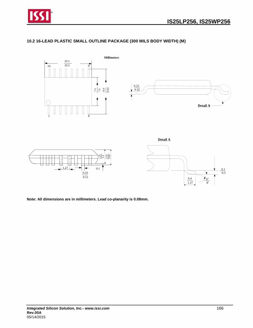
IS25LP256, IS25WP256
Integrated Silicon Solution, Inc.- www.issi.com 166 Rev.00A 05/14/2015
10.2 16-LEAD PLASTIC SMALL OUTLINE PACKAGE (300 MILS BODY WIDTH) (M)
1.27
0.51
0.33
2.4
2.25
2.35
2.65
0.1
80 0
01.27
0.4
Detail A
Detail A
0.23
Millimeters
1 8
916 10.5
10.1
7.4
7.6
10.0
10.6
5
0.32
0.10.3
Note: All dimensions are in millimeters. Lead co-planarity is 0.08mm.
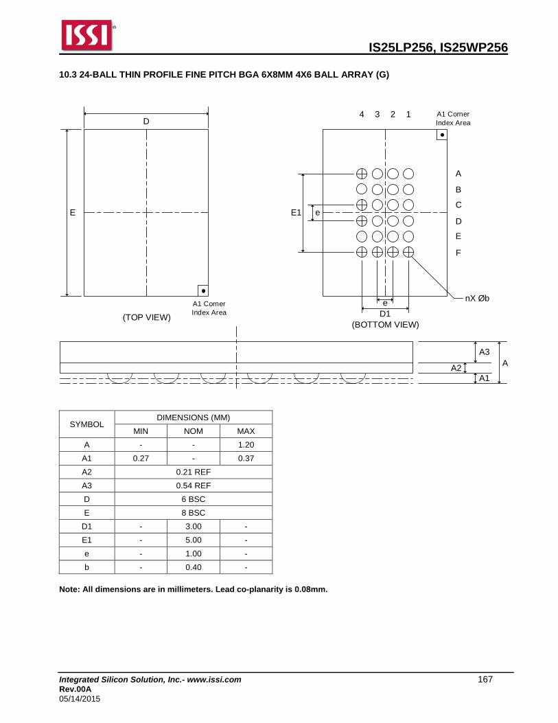
IS25LP256, IS25WP256
Integrated Silicon Solution, Inc.- www.issi.com 167 Rev.00A 05/14/2015
10.3 24-BALL THIN PROFILE FINE PITCH BGA 6X8MM 4X6 BALL ARRAY (G)
D
E
4 3 2 1
A
B
C
D
E
F
E1 e
D1
AA3
A2A1
e nX Øb
(TOP VIEW)
A1 CornerIndex Area
(BOTTOM VIEW)
A1 CornerIndex Area
SYMBOL DIMENSIONS (MM)
MIN NOM MAX
A - - 1.20
A1 0.27 - 0.37
A2 0.21 REF
A3 0.54 REF
D 6 BSC
E 8 BSC
D1 - 3.00 -
E1 - 5.00 -
e - 1.00 -
b - 0.40 -
Note: All dimensions are in millimeters. Lead co-planarity is 0.08mm.

IS25LP256, IS25WP256
Integrated Silicon Solution, Inc.- www.issi.com 168 Rev.00A 05/14/2015
10.4 24- BALL THIN PROFILE FINE PITCH BGA 6X8MM 5X5 BALL ARRAY (H)
D
E
4 3 2 1
A
B
C
D
E
E1e
D1
AA3
A2A1
e
nX Øb
(TOP VIEW)
A1 CornerIndex Area
(BOTTOM VIEW)
A1 CornerIndex Area
5
SYMBOL DIMENSIONS (MM)
MIN NOM MAX
A - - 1.20
A1 0.27 - 0.37
A2 0.21 REF
A3 0.54 REF
D 6 BSC
E 8 BSC
D1 - 4.00 -
E1 - 4.00 -
e - 1.00 -
b - 0.40 -
Note: All dimensions are in millimeters. Lead co-planarity is 0.08mm.
IS25LP256, IS25WP256
Integrated Silicon Solution, Inc.- www.issi.com 169 Rev.00A 05/14/2015
11. ORDERING INFORMATION – Valid Part Numbers
IS25LP256 - J B L E
TEMPERATURE RANGE E = Extended (-40°C to +105°C) E1 = Extended+ (-40°C to +125°C) A1 = Automotive Grade (-40°C to +85°C) A2 = Automotive Grade (-40°C to +105°C) A3 = Automotive Grade (-40°C to +125°C) PACKAGING CONTENT L = RoHS compliant PACKAGE Type L = 8-contact WSON (8x6mm) M = 16-pin SOIC 300mil G = 24-ball TFBGA (6x8mm) 4x6 ball array (1) H = 24-ball TFBGA (6x8mm) 4x6 ball array (1) W = KGD (Call Factory) Option J = Standard R = additional RESET# pin option Die Revision Blank = First Revision Density 256 = 256 Megabit BASE PART NUMBER IS = Integrated Silicon Solution Inc. 25LP = FLASH, 2.30V ~ 3.60V, QPI 25WP = FLASH, 1.65V ~ 1.95V, QPI
Note: 1. For the additional RESET# pin option for 24-ball TFBGA 6x8mm packages, call Factory

IS25LP256, IS25WP256
Integrated Silicon Solution, Inc.- www.issi.com 170 Rev.00A 05/14/2015
Notes: 1. A*= A1, A2, A3: Meets AEC-Q100 requirements with PPAP, E1= Extended+ non-Auto qualified Temp Grades: E= -40 to 105°C, E1= -40 to 125°C, A1= -40 to 85°C, A2= -40 to 105°C, A3= -40 to 125°C 2. The dedicated parts have additional RESET# pin on pin3. 3. For the additional RESET# pin option for 24-ball TFBGA 6x8mm packages, call Factory.
Density, Voltage Frequency (MHz) Order Part Number(1) Package
256M, 3V
STR 166, DTR 80
IS25LP256-JLLE IS25LP256-JLLE1 8-contact WSON 8x6mm
IS25LP256-JMLE IS25LP256-JMLE1 16-pin SOIC 300mil
IS25LP256-JGLE IS25LP256-JGLE1 24-ball TFBGA 6x8mm 4x6 ball array(3)
IS25LP256-JHLE IS25LP256-JHLE1 24-ball TFBGA 6x8mm 5x5 ball array(3)
IS25LP256-RMLE IS25LP256-RMLE1 16-pin SOIC 300mil(2)
IS25LP256-JLLA* 8-contact WSON (8x6mm) (Call Factory)
IS25LP256-JMLA* 16-pin SOIC 300mil (Call Factory)
IS25LP256-JGLA* 24-ball TFBGA 6x8mm 4x6 ball array(3) (Call Factory)
IS25LP256-JHLA* 24-ball TFBGA 6x8mm 5x5 ball array(3) (Call Factory)
IS25LP256-RMLA* 16-pin SOIC 300mil(2) (Call Factory)
IS25LP256-JWLE KGD (Call Factory)
256M, 1.8V
STR 166, DTR 80
IS25WP256-JLLE IS25WP256-JLLE1 8-contact WSON 8x6mm
IS25WP256-JMLE IS25WP256-JMLE1 16-pin SOIC 300mil
IS25WP256-JGLE IS25WP256-JGLE1 24-ball TFBGA 6x8mm 4x6 ball array(3)
IS25WP256-JHLE IS25WP256-JHLE1 24-ball TFBGA 6x8mm 5x5 ball array(3)
IS25WP256-RMLE IS25WP256-RMLE1 16-pin SOIC 300mil(2)
IS25WP256-JLLA* 8-contact WSON (8x6mm) (Call Factory)
IS25WP256-JMLA* 16-pin SOIC 300mil (Call Factory)
IS25WP256-JGLA* 24-ball TFBGA 6x8mm 4x6 ball array(3) (Call Factory)
IS25WP256-JHLA* 24-ball TFBGA 6x8mm 5x5 ball array(3) (Call Factory)
IS25WP256-RMLA* 16-pin SOIC 300mil(2) (Call Factory)
IS25WP256-JWLE KGD (Call Factory)


![IFRS Core Tools Afl]jfYlagfYd?99H](https://img.pdfslide.us/doc/110x75/5e7fac90e4a4cd6eb0789836/-ifrs-core-tools-afljfylagfyd99h-.jpg)