Embed Size (px)
Citation preview
Lecture 17The Bipolar Junction Transistor (I)
Forward Active Regime
Outline
• The Bipolar Junction Transistor (BJT): – structure and basic operation
• IV characteristics in forward active regime
Reading Assignment: Howe and Sodini; Chapter 7, Sections 7.1, 7.2
6.012 Spring 2009 Lecture 17 1
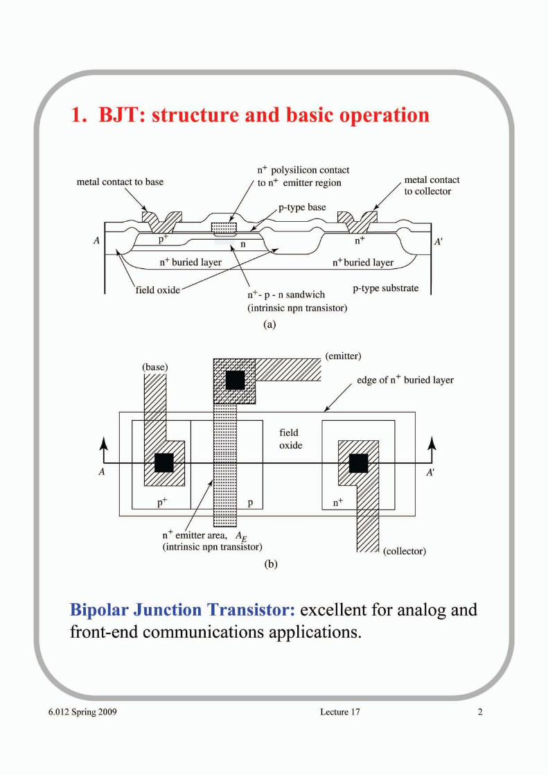
1. BJT: structure and basic operation
n+ polysilicon contact metal contact to base to n+ emitter region
\ /
A'
I 'field oxide n+-p - n sandwich
(intrinsic npn transistor)
(a)
edge of n+ buried layer
Bipolar Junction Transistor: excellent for analog and fkont-end communications applications.
6.012Spring 2009 Lecture17'
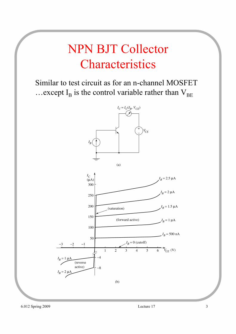
NPN BJT Collector Characteristics
Similar to test circuit as for an nchannel MOSFET …except IB is the control variable rather than VBE
VCE
IC
= IC
(IB, V
CE)
(a)
1
50
100
150
200
250
300
IC�
(µA)
VCE
(V)6
(b)
−1−2−3
−4
−8
IB = 1 µA
IB = 2 µA
(reverse�
active)
(forward active)
(saturation)
IB = 0 (cutoff)
IB = 500 nA
IB = 1 µA
IB = 1.5 µA
IB = 2 µA
IB = 2.5 µA
IB
+
−
5432
6.012 Spring 2009 Lecture 17 3
• Close enough for minority carriers to interact – ⇒ can diffuse quickly through the base
• Far apart enough for depletion regions not to interact – ⇒ prevent “punchthrough”
Simplified onedimensional model of intrinsic device: Emitter Base Collector
IE
IB
IC
WB-XBE WB+XBC WB+XBC+WC-WE-XBE
VBE VBC +
-
+
-
x 0
Regions of operation:
saturation
reverse cut-off
forward�
active
VBC
VBC
VCE
VBE
VBE
B
C
E
+
-
+
- +
-
VCE = VBEVBC
n p n
NaBNdE NdC
6.012 Spring 2009 Lecture 17 4
BJT=two neighboring pn junctions back-to-back
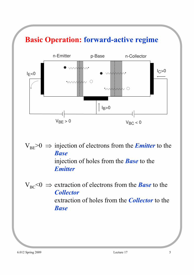
Basic Operation: forwardactive regime
VBE>0 ⇒ injection of electrons from the Emitter to the Base injection of holes from the Base to the Emitter
VBC<0 ⇒ extraction of electrons from the Base to the Collector extraction of holes from the Collector to the Base
n-Emitter p-Base n-Collector
IE<0
IB>0
IC>0
VBE > 0 VBC < 0
6.012 Spring 2009 Lecture 17 5
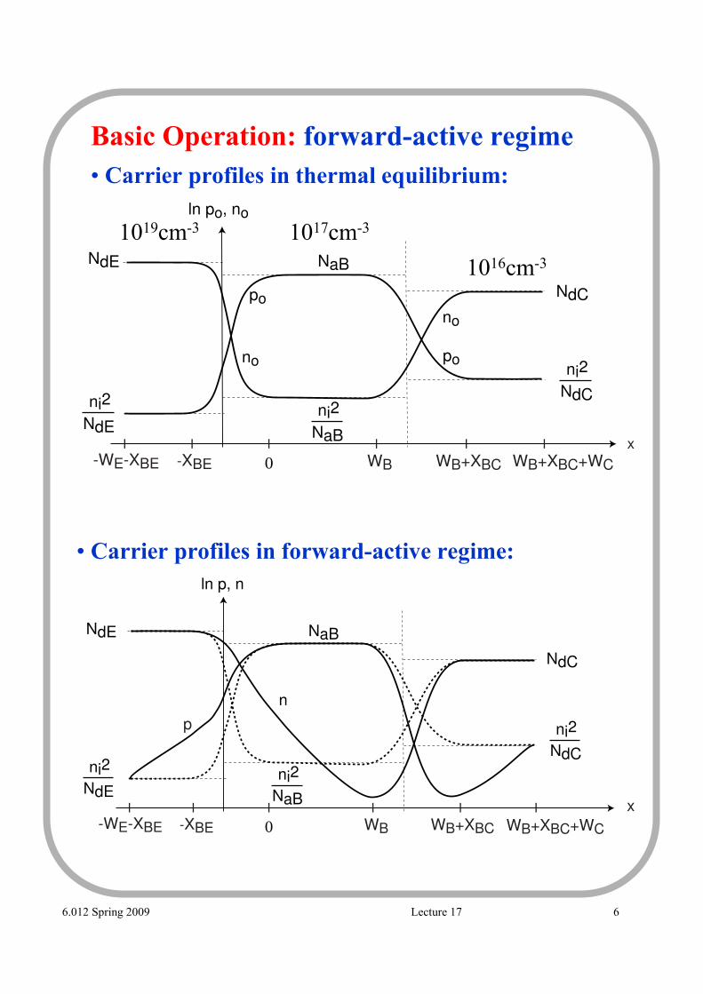
Basic Operation: forwardactive regime • Carrier profiles in thermal equilibrium:
• Carrier profiles in forwardactive regime:
ln po, no
po
pono
no
NdE
NdC
ni2
NdE ni2
NaB
ni2
NdC
0
NaB
WB-XBE WB+XBC -WE-XBE WB+XBC+WC
x
ln p, n
n
NdE
NdC
ni2
NdE ni2
NaB
ni2
NdC
0
NaB
WB-XBE WB+XBC -WE-XBE
p
WB+XBC+WC
x
1019cm3 1017cm3
1016cm3
6.012 Spring 2009 Lecture 17 6
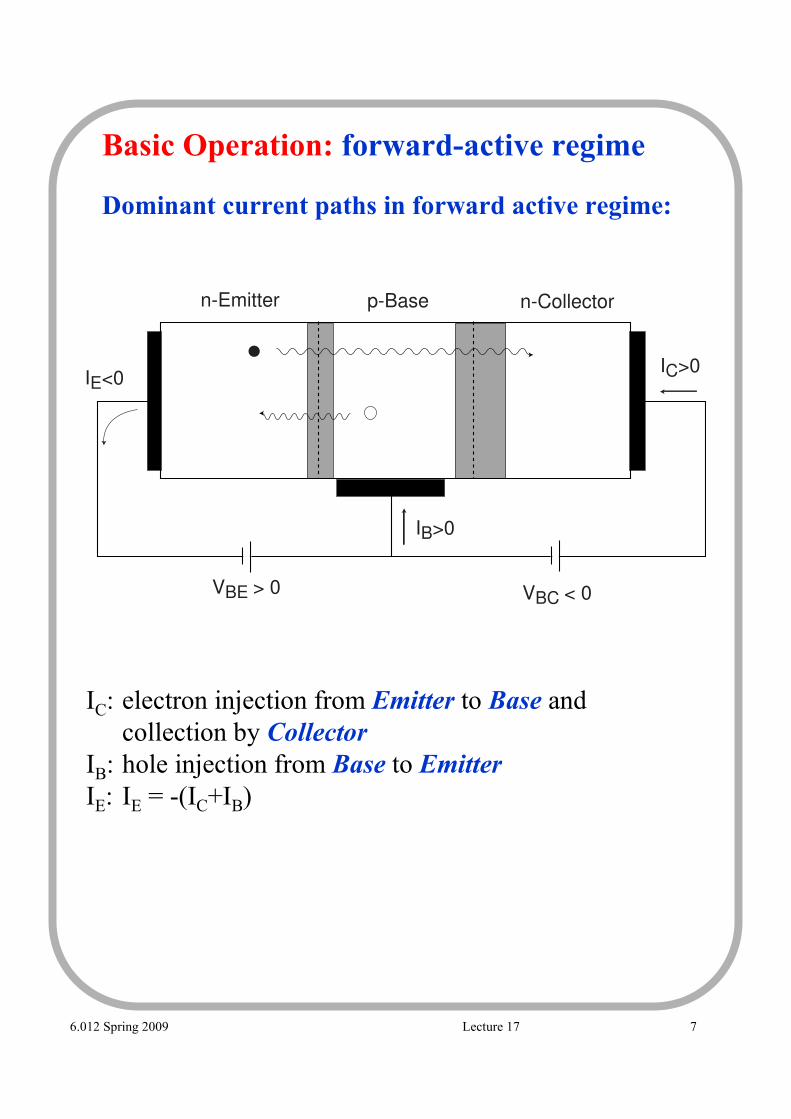
Basic Operation: forwardactive regime
Dominant current paths in forward active regime:
n-Emitter p-Base n-Collector
IE<0
IB>0
IC>0
VBE > 0 VBC < 0
IC: electron injection from Emitter to Base and collection by Collector
IB: hole injection from Base to Emitter IE: IE = (IC+IB)
6.012 Spring 2009 Lecture 17 7
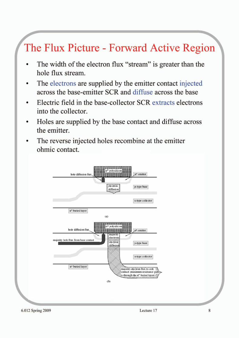
The width of the electron flux "stream" is greater than the hole flux stream.
The electrons are supplied by the emitter contact injected across the base-emitter SCR and difhse across the base Electric field in the base-collector SCR extracts electrons into the collector. Holes are supplied by the base contact and diffuse across the emitter. The reverse injected holes recombine at the emitter
nic contact. -........................................ -..............-........................................-..............-........................................ -..............-............... ..............K::::::::::::::"................+ po1ysiliwn:iii:i;i::iii:
6.012Spring 2000 Lecture I?
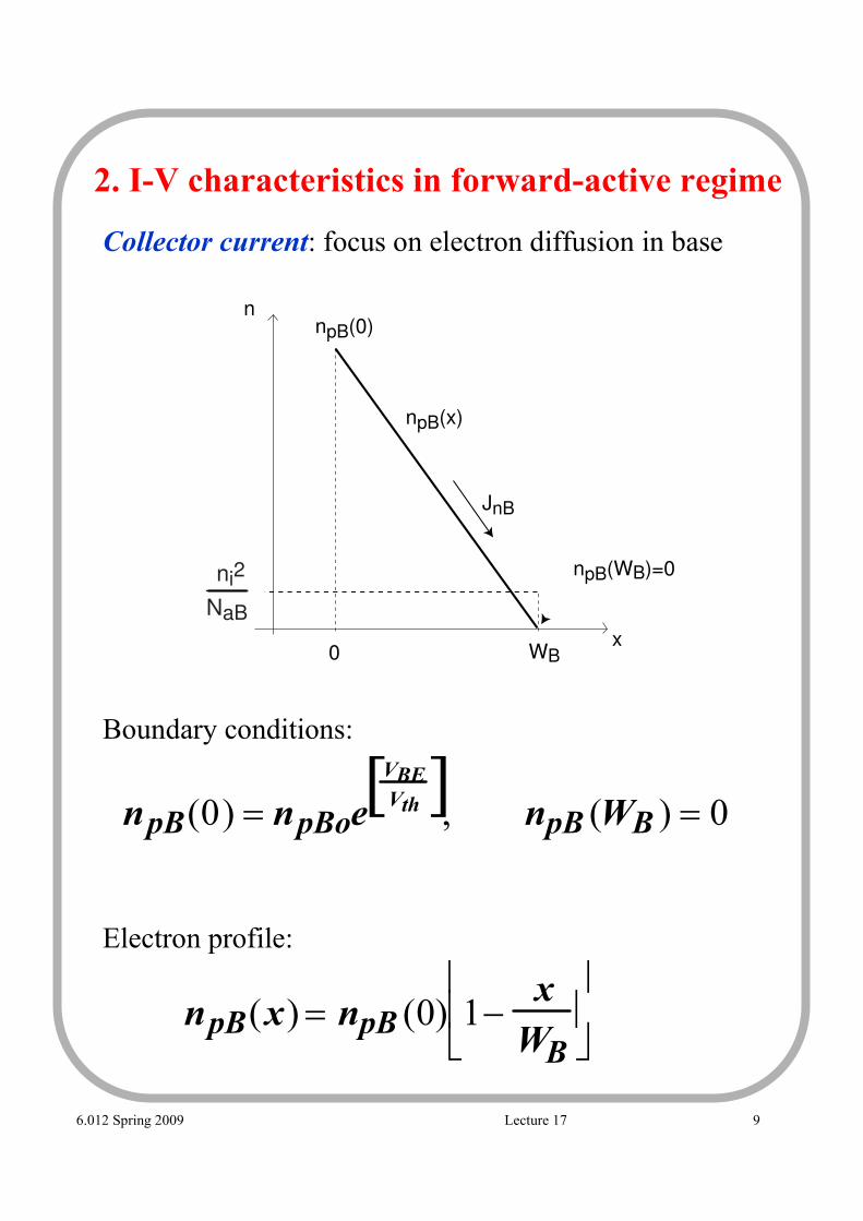
2. IV characteristics in forwardactive regime
npB(0) = npBoe VBE Vth[ ]
, npB (WB ) = 0
Collector current: focus on electron diffusion in base
Electron profile:
Boundary conditions:
npB(x) = npB (0) 1− x WB
n
x 0
npB(0)
JnB
npB(WB)=0
npB(x)
WB
ni2
NaB
6.012 Spring 2009 Lecture 17 9
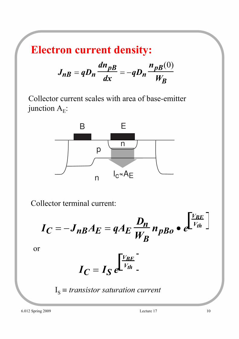
Electron current density:
Collector current scales with area of baseemitter junction AE:
IC = −JnB AE = qAE Dn WB
npBo • e VBE Vth[ ]
Collector terminal current:
JnB = qDn dnpB
dx = −qDn
npB(0)
WB
or
IC = IS e VBE Vth[ ]
IS ≡ transistor saturation current
�
Ic AE
B E
n p
n
6.012 Spring 2009 Lecture 17 10
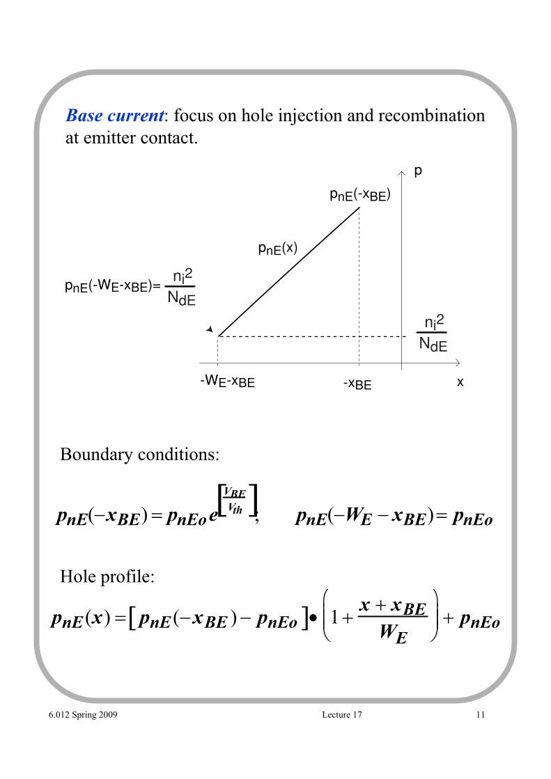
Base current: focus on hole injection and recombination at emitter contact.
Boundary conditions:
Hole profile:
pnE(−xBE) = pnEo e VBE Vth[ ]
; pnE(−WE − xBE) = pnEo
pnE(x) = pnE(−xBE ) − pnEo[ ]• 1 + x + xBE WE
+ pnEo
p
x-xBE
pnE(x)
pnE(-xBE)
-WE-xBE
ni2
NdE
pnE(-WE-xBE)= ni2
NdE
6.012 Spring 2009 Lecture 17 11
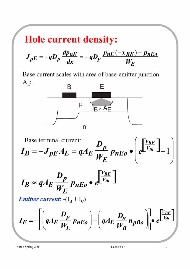
Hole current density:
Base current scales with area of baseemitter junction AE:
IB = −J pE AE = qAE Dp
WE pnEo • e
VBE Vth[ ]−1
IB ≈ qAE Dp
WE pnEo • e
VBE Vth[ ]
Base terminal current:
J pE = −qDp dpnE dx
= −qDp pnE (−xBE ) − pnEo
WE
�
IB AE
B E
p
n
Emitter current: (IB + IC)
IE = − qAE Dp
WE pnEo
+ qAE
Dn WB
npBo
• e
VBE Vth[ ]
6.012 Spring 2009 Lecture 17 12
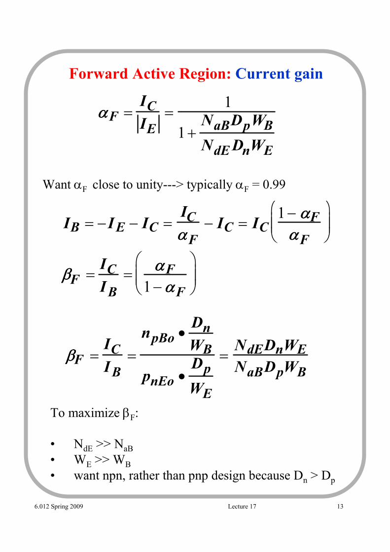
Forward Active Region: Current gain
ββββF = IC IB
=
npBo • Dn WB
pnEo • Dp
WE
= NdEDnWE NaBDpWB
To maximize βF:
• NdE >> NaB
• WE >> WB
• want npn, rather than pnp design because Dn > D p
ααααF = IC IE
= 1
1 + NaBDpWB
NdE DnWE
Want αF close to unity> typically αF = 0.99
IB = −IE − IC = IC ααααF
− IC = IC 1 − ααααF
ααααF
ββββF = IC IB
= ααααF 1 − ααααF
6.012 Spring 2009 Lecture 17 13
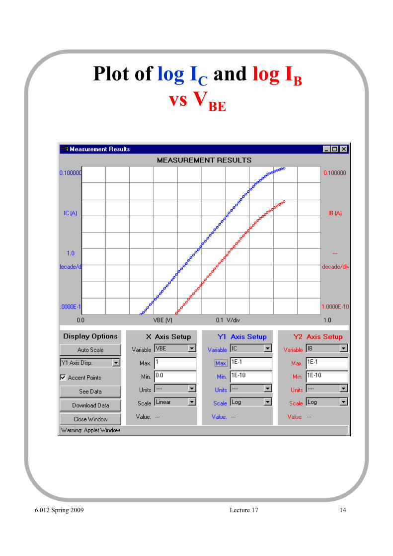
Plot of log IC and log IB
vs VBE
6.012 Spring 2009 Lecture 17 14
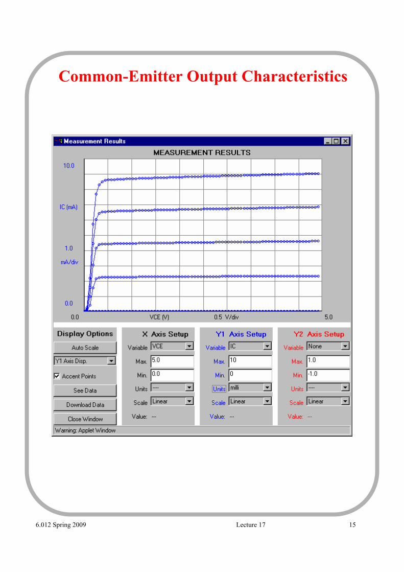
CommonEmitter Output Characteristics
6.012 Spring 2009 Lecture 17 15
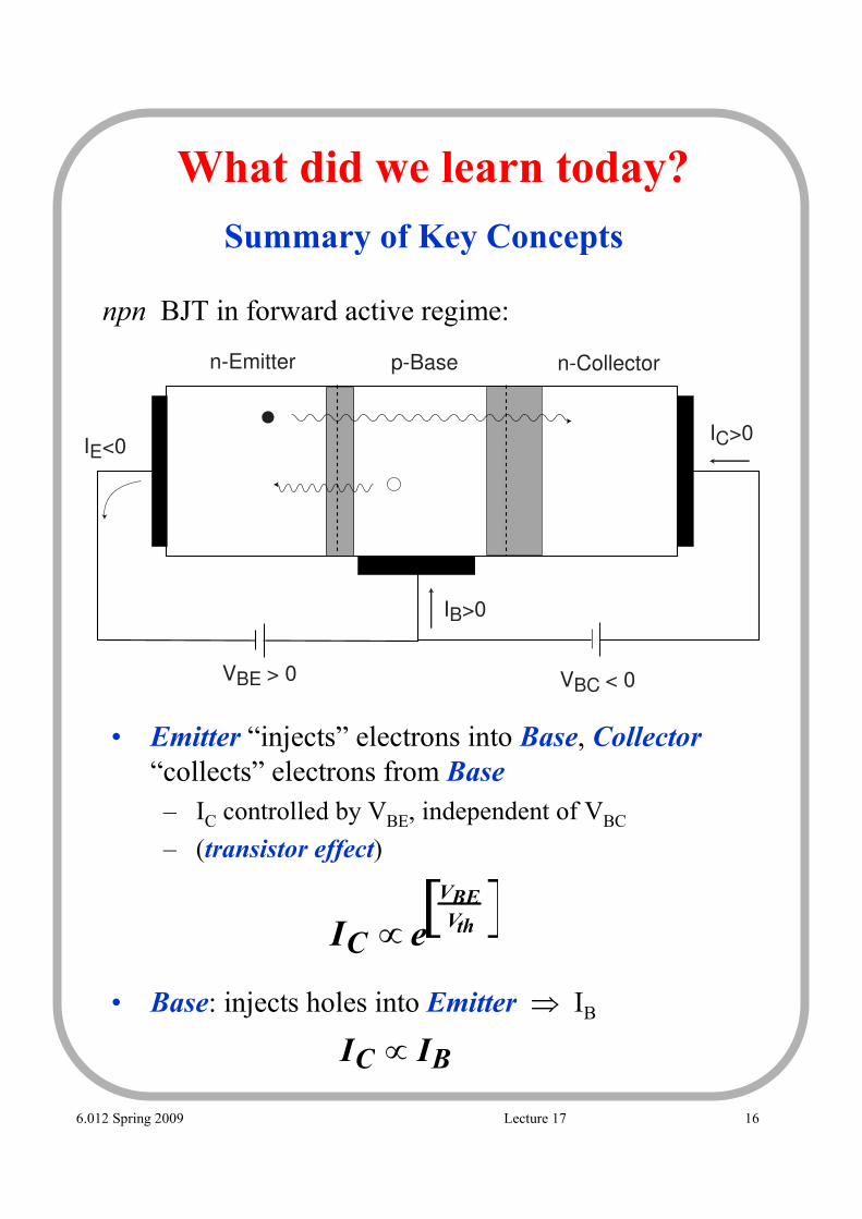
What did we learn today?
• Emitter “injects” electrons into Base, Collector “collects” electrons from Base – IC controlled by VBE, independent of VBC
– (transistor effect)
• Base: injects holes into Emitter ⇒ IB
npn BJT in forward active regime:
IC ∝ e VBE Vth[ ]
IC ∝ IB
n-Emitter p-Base n-Collector
IE<0
IB>0
IC>0
VBE > 0 VBC < 0
Summary of Key Concepts
6.012 Spring 2009 Lecture 17 16
MIT OpenCourseWarehttp://ocw.mit.edu
6.012 Microelectronic Devices and Circuits Spring 2009
For information about citing these materials or our Terms of Use, visit: http://ocw.mit.edu/terms.


![[ Sedra] Microelectronic Circuits(b Ok.org)](https://img.pdfslide.us/doc/110x75/617b73ef7012c349660bd625/-sedra-microelectronic-circuitsb-okorg.jpg)


