Embed Size (px)
Citation preview
6.012 - Electronic Devices and CircuitsLecture 19 - Differential Amplifier Stages - Outline
• AnnouncementsHandouts - Lecture Outline and SummaryDesign Problem - out tomorrow in recitation
• Review - Single-transistor building block stagesCommon emitter/source: general purpose gain stage, workhorseCommon base/gate: small Rin, large Rout, unity Ai, same Av as CE/SEmitter/source follower: large Rin, small Rout, unity Av, same Ai as CE/SSeries and Shunt feedback: we'll see in special situations
• Differential Amplifier Stages - Large signal behaviorGeneral features: symmetry, inputs, outputs, biasing (Symmetry is the key!)Large signal transfer characteristic
• Difference- and common-mode signalsDecomposing and reconstructing general signals
• Half-circuit incremental analysis techniquesLinear equivalent half-circuitsDifference- and common-mode analysisExample: analysis of emitter-coupled pair
Clif Fonstad, 11/03 Lecture 19 - Slide 1
IBIAS
V-
V+
vout+
-vin+-
CE
CO
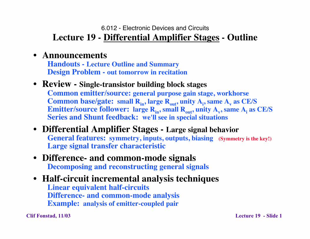
• The "mid-band"concept: frequency range of constant gain and phase
Commonemitter
LEC for common emitter stagewith all the capacitors
Common emitter LEC for in mid-band range Note: gl = gLOAD + gnext
Biasing capacitors: typically in mF range(CO, CE, etc.) effectively shorts above wLODevice capacitors: typically in pF range (Cp, Cm, etc.) effectively open until wHI
Mid-band frequencies defined as wLO < w < wHI
Clif Fonstad, 11/03 Lecture 19 - Slide 2
gp
+
-vp
+
-
v in
v t+-
rt gmvp go
+
-
voutgLOAD
rIBIAS CE
COCm
Cp gnext
gp
+
-vp gmvp go gl
+
-v in
+
-voutv t
+-
rt
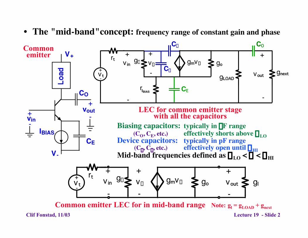
• Summary of the stages (bipolar)
Clif Fonstad, 11/03 Lecture 19 - Slide 3
†
Voltagegain, Av
Currentgain, Ai
Inputresistance, Ri
Outputresistance, Ro
Common emitter -gm
go + gl[ ]= -gmrl '( ) -
b gl
go + gl[ ]rp ro =
1go
Ê
Ë Á
ˆ
¯ ˜
Common base gm
go + gl[ ]= gmrl '( ) ª1 ª
rp
b +1[ ]ª b +1[ ] ro
Emitter follower gm + gp[ ]gm + gp + go + gl[ ]
ª1 bgl
go + gl[ ]ª b rp + b +1[ ]rl ' ª
rt + rp
b +1[ ]Emitter degeneration
(series feedback) ª - rl
RF
ª b ª rp + b +1[ ]RF ª ro
Shunt feedback -gm - GF[ ]go + GF[ ]
ª -gmRF -gl
GF
1gp + GF 1- Av[ ]
ro RF =1
go + GF[ ]
Ê
Ë Á
ˆ
¯ ˜

• Summary of the stages (MOSFET)
Clif Fonstad, 11/03 Lecture 19 - Slide 4
†
Voltagegain, Av
Currentgain, Ai
Inputresistance, Ri
Outputresistance, Ro
Common source -gm rl ' • • ro =1go
Ê
Ë Á
ˆ
¯ ˜
Common gate ª gm + gmb[ ] rl ' ª1 ª1
gm + gmb[ ]ª ro 1+
gm + gmb + go[ ]gt
Ï Ì Ó
¸ ˝ ˛
Source follower gm
gm + go + gl[ ]ª1 • •
1gm + go + gl[ ]
ª1gm
Source degeneration(series feedback) ª - rl
RF
• • ª ro
Shunt feedback -gm - GF[ ]go + GF[ ]
ª -gmRF -gl
GF
RF
GF 1- Av[ ]ro RF =
1go + GF[ ]
Ê
Ë Á
ˆ
¯ ˜
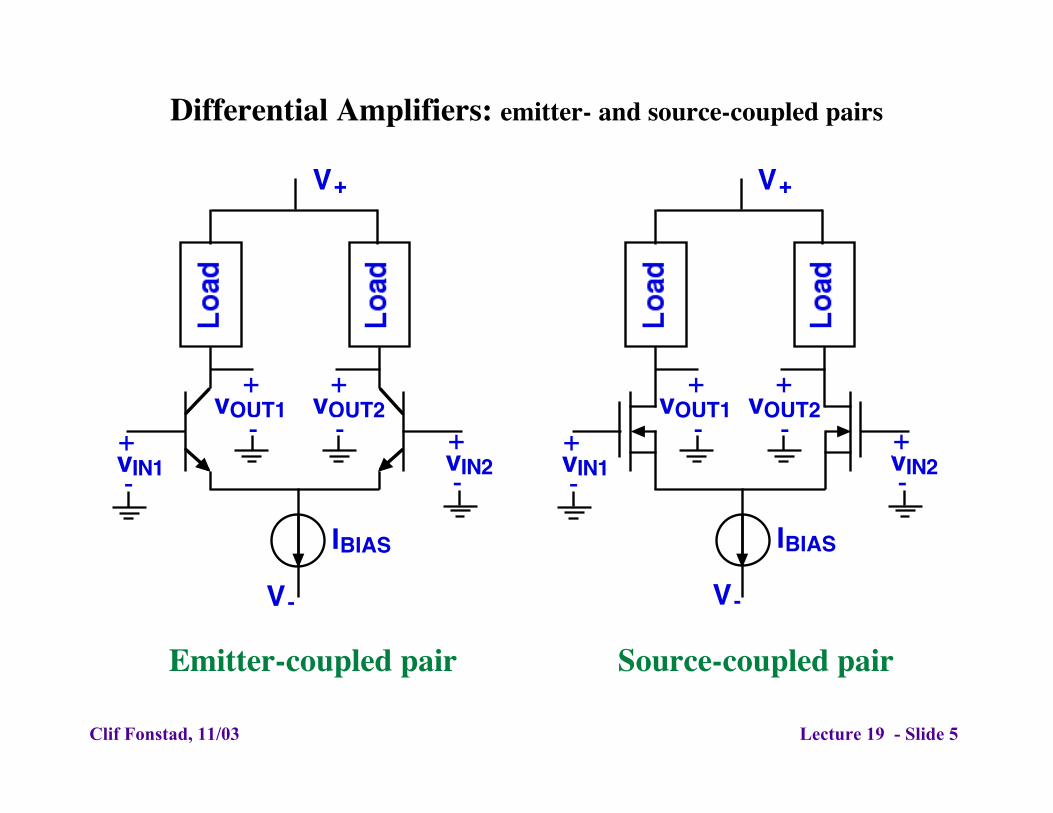
Differential Amplifiers: emitter- and source-coupled pairs
V+
vIN1
vOUT1+-
vOUT2+-+
-vIN2+-
IBIAS
V-V-
V+
vIN1+-
vOUT1+-
vOUT2+-
vIN2+-
IBIAS
Emitter-coupled pair Source-coupled pair
Clif Fonstad, 11/03 Lecture 19 - Slide 5
Emitter-coupled pair: large signal analysis
Above: Circuit with large signal,FAR BJT model in place
Right: Transfer characteristic
Clif Fonstad, 11/03 Lecture 19 - Slide 6
Analysis: 3 KVL loops (see text)Result: Outputs only depend on difference
between the two inputs, (vI1-vI2)
Transfer characteristic is symmetrical
†
vO1 = VCC -aF RC IBIAS
1 + e -q v I 1 -v I 2[ ] kT{ }vO2 = VCC -
aF RC IBIAS
1 + e q v I 1 -v I 2[ ] kT{ }
vO = -aF RC IBIAS tanh q vI1 - vI 2[ ]2kT
Slope near origin = -gmRC

Clif Fonstad, 11/03 Lecture 19 - Slide 7
Above: Circuit with largesignal, MOSFET modelfor saturation in place
Right: Transfer characteristic
Source-coupled pair: large signal analysis
Analysis: 3 KVL loops (see text)Result: Outputs only depend on difference
between the two inputs, (vI1-vI2)
Transfer characteristic is symmetrical†
vO1 = VDD -RD
2
K vIN1 - vIN 2[ ]2+ IBIAS
+K2
vIN1 - vIN 2[ ] 4IBIAS
K- vIN1 - vIN 2[ ]2
Ï
Ì Ô
Ó Ô
¸
˝ Ô
˛ Ô
vO2 = VDD -RD
2
K vIN1 - vIN 2[ ]2+ IBIAS
-K2
vIN1 - vIN 2[ ] 4IBIAS
K- vIN1 - vIN 2[ ]2
Ï
Ì Ô
Ó Ô
¸
˝ Ô
˛ Ô
†
vO = -RDK
2vIN1 - vIN 2[ ] 4IBIAS
K- vIN1 - vIN 2[ ]2
Slope near origin = -gmRD

Differential Amplifier Analysis -difference- and common-mode signals
Any pair of signals can be decomposed into a portion that is theidentical in both, and a portion that is equal, but opposite in both. Forexample, if we have two voltages, v1 and v2, we can define a common-mode signal, vC, and a difference-mode signal, vD, as:
In terms of these two voltages, we can write v1 and v2 as:
In incremental analysis of linear amplifiers we will decom-pose ourinputs into difference- and common-mode inputs:
We will apply vid to the circuit and get vod (= Avdvid), and then applyvic to the circuit to get voc (= Avcvic). Then we will reconstruct ouroutputs:
Clif Fonstad, 11/03 Lecture 19 - Slide 8
†
vC ≡ v1 + v2[ ] 2 vD ≡ v1 - v2[ ]
†
v1 = vC + vD 2 v2 = vC - vD 2
†
vic ≡ vin1 + vin2[ ] 2 vid ≡ vin1 - vin2[ ]
†
vout1 = voc + vod 2 = Avcvic + Avd vid 2vout2 = voc - vod 2 = Avcvic - Avd vid 2
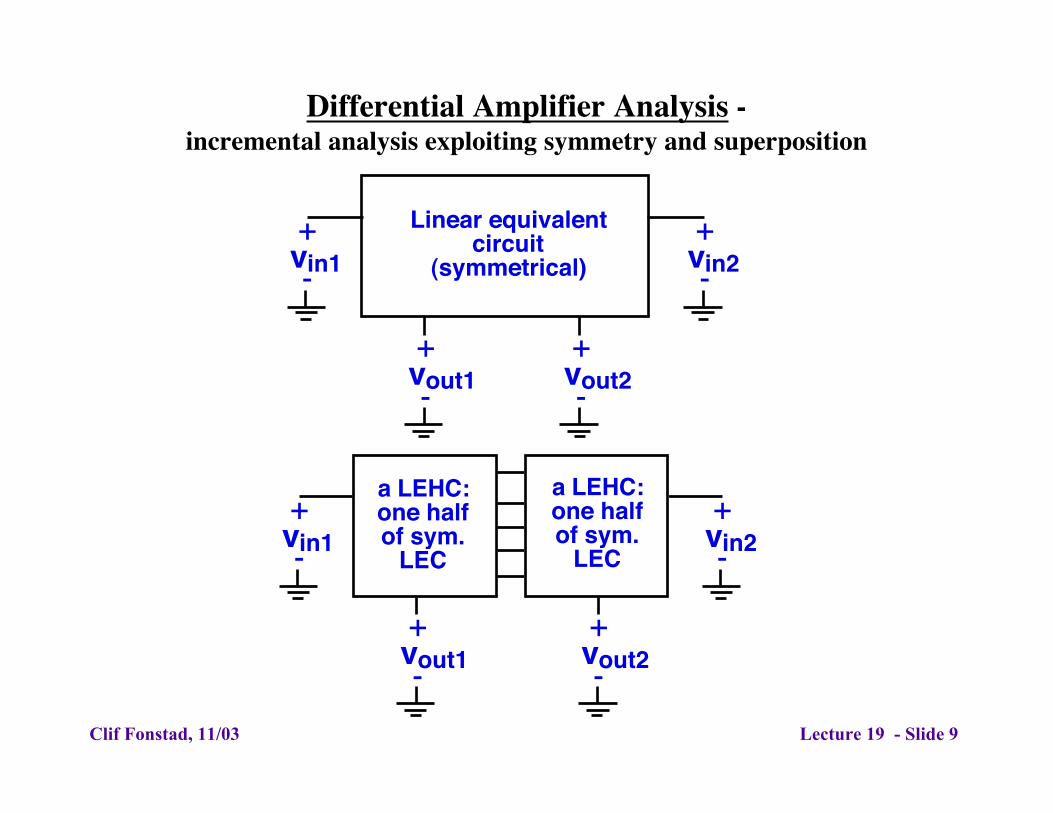
vin1+- vin2
+-
vout1+- vout2
+-
Linear equivalentcircuit
(symmetrical)
vin2+-
vout2+-
vin1+-
vout1+-
a LEHC: one halfof sym.
LEC
a LEHC: one halfof sym.
LEC
Differential Amplifier Analysis -incremental analysis exploiting symmetry and superposition
Clif Fonstad, 11/03 Lecture 19 - Slide 9
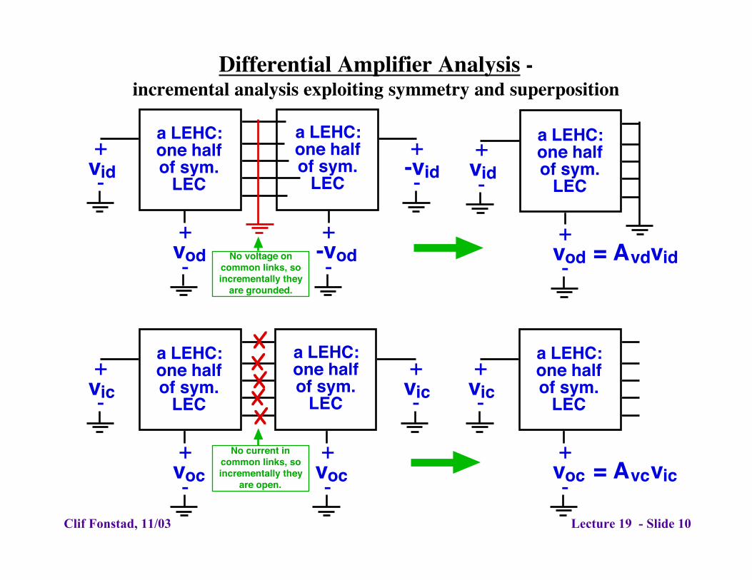
-vid+-
-vod+-
a LEHC: one halfof sym.
LEC vid+-
vod+-
a LEHC: one halfof sym.
LEC
No voltage on common links, so incrementally they
are grounded.
vid+-
vod = Avdvid+-
a LEHC: one halfof sym.
LEC
vic+-
voc+-
a LEHC: one halfof sym.
LEC vic+-
voc+-
a LEHC: one halfof sym.
LEC
No current in common links, so incrementally they
are open.
vic+-
voc = Avcvic+-
a LEHC: one halfof sym.
LEC
Differential Amplifier Analysis -incremental analysis exploiting symmetry and superposition
Clif Fonstad, 11/03 Lecture 19 - Slide 10
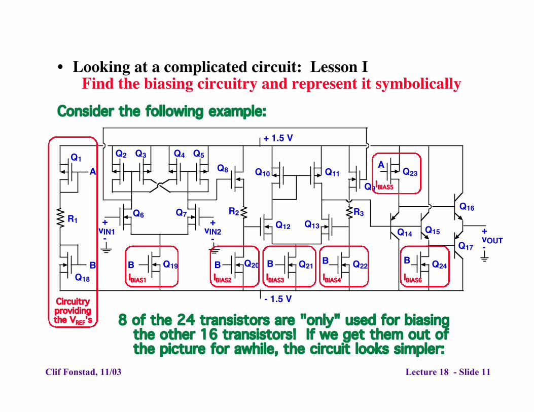
Q1
A
BQ18
R1
Q5Q4Q3Q2
Q9
vIN2
+ 1.5 V
- 1.5 V
B
vIN1+-
Q6+-
Q7
Q19 B
Q12 Q13
Q21B B
Q11Q10Q8
Q20 Q22 Q24
Q15
Q16
Q17vOUT+-
B
A
Q14
Q23
R2 R3
• Looking at a complicated circuit: Lesson IFind the biasing circuitry and represent it symbolically
Consider the following example:
Clif Fonstad, 11/03 Lecture 18 - Slide 11
Circuitryprovidingthe VREF's
IBIAS1 IBIAS2 IBIAS3 IBIAS4
IBIAS5
IBIAS6
8 of the 24 transistors are "only" used for biasingthe other 16 transistors! If we get them out ofthe picture for awhile, the circuit looks simpler:
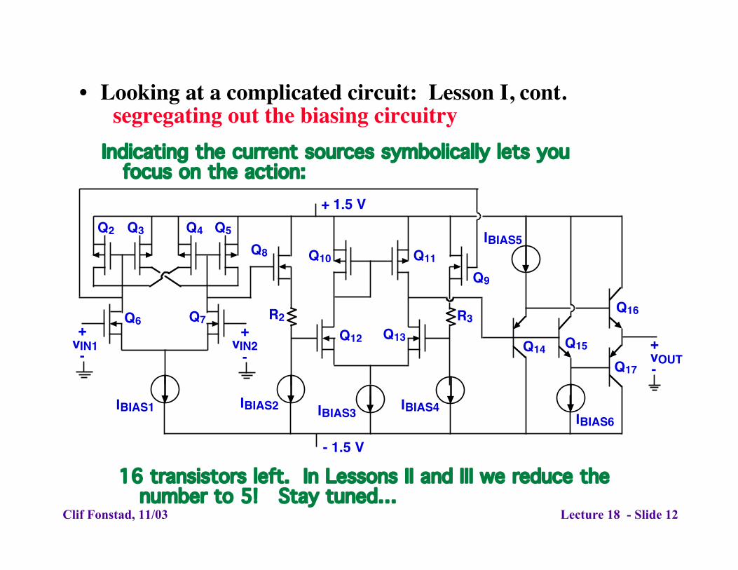
• Looking at a complicated circuit: Lesson I, cont.segregating out the biasing circuitry
Indicating the current sources symbolically lets youfocus on the action:
Clif Fonstad, 11/03 Lecture 18 - Slide 12
IBIAS1 IBIAS2 IBIAS3 IBIAS4IBIAS6
Q5Q4Q3Q2
Q9
vIN2
+ 1.5 V
- 1.5 V
vIN1+-
Q6+-
Q7Q12 Q13
Q11Q10Q8
Q15
Q16
Q17vOUT+-
Q14
R2 R3
IBIAS5
16 transistors left. In Lessons II and III we reduce thenumber to 5! Stay tuned…
Clif Fonstad, 11/03 Lecture 19 - Slide 13
IBIAS1 IBIAS2 IBIAS3 IBIAS4IBIAS6
Q5Q4Q3Q2
Q9
vIN2
+ 1.5 V
- 1.5 V
vIN1+-
Q6+-
Q7Q12 Q13
Q11Q10Q8
Q15
Q16
Q17vOUT+-
Q14
R2 R3
IBIAS5Current mirror load
Lee load
Differential Amplifier Analysis - an example of half circuitreduction
Difference-mode half circuit Common-mode half circuit
vod+
-vid/2+
-
Q6 Q12
Q16
Q9
Q14
R3
roQ22
roQ23reLLdm reCMdm
voc+
-vic
+
-
Q6 Q12
Q16
Q9
Q14
R3
roQ22
roQ23reLLcm reCMcm
2roQ19 2roQ21
6.012 - Electronic Devices and CircuitsLecture 19 - Differential Amplifier Stages - Summary
• Differential Amplifier Stages - Large signal behaviorGeneral features: two transistors (an emitter-coupled, or source-coupled, pair)
highly symmetricaltwo inputs, two outputs (however, one input can be zero)biased by single current source
Large signal transfer characteristics: only depends on vIN1 - vIN2
• Difference- and common-mode signalsDifference-mode: vID = vIN1 - vIN2Common-mode: vIC = (vIN1 + vIN2)/2Reconstruction: vIN1 = vIC + vID/2, vIN2 = vIC - vID/2
• Half-circuit incremental analysis techniquesExploiting symmetry and superpositionDifference-mode lin. equiv. half-circuit: links are groundedCommon-mode lin. equiv. half circuit: links are cut, open circuitedApproach: 1. identify common- and difference-mode half circuits
2. calculate common- and difference-mode signals3. analyze difference-mode half-circuit (each half-circuit is one of4. analyze common-mode half-circuit our known building-blocks)5. reconstruct signals
Clif Fonstad, 11/03 Lecture 19 - Slide 14