Embed Size (px)
Citation preview

Diodes for IGCT- and GTO Applications
Application Note
Applying Fast Recovery Diodes

Page 2 of 20 Doc. No. 5SYA2064-01 Dec. 08
Applying Fast Recovery Diodes
Application Note
Thomas Setz
ABB Switzerland Ltd
Semiconductors
December 2008
Table of Contents:
1 INTRODUCTION.....................................................................................................................................................3
2 FAST RECOVERY DIODE PRODUCT RANGE FROM ABB ..........................................................................3 2.1 GTO DIODES .......................................................................................................................................................3
2.1.1 GTO Freewheeling Diodes .........................................................................................................................3 2.1.2 Snubber Diodes...........................................................................................................................................4
2.2 IGCT DIODES ......................................................................................................................................................4 3 DATA SHEET USERS GUIDE ...............................................................................................................................5
3.1 IGCT-DIODE DATA SHEET ...................................................................................................................................5 4 DESIGN RECOMMENDATIONS........................................................................................................................15
4.1 DETERMINE THE RIGHT DIODE FOR STANDARD APPLICATION CONDITIONS..........................................................15 4.2 DETERMINE THE RIGHT DIODE FOR CUSTOMIZED APPLICATION CONDITIONS ......................................................16 4.3 DIODE SWITCHING AND IMPORTANT PARAMETERS TO CONSIDER........................................................................17
4.3.1 Diode turn-on............................................................................................................................................17 4.3.2 Diode turn-off ...........................................................................................................................................19 4.3.3 Surge current rating..................................................................................................................................19
5 ADDITIONAL NOTES ..........................................................................................................................................20 5.1 REFERENCES......................................................................................................................................................20 5.2 APPLICATION SUPPORT.......................................................................................................................................20

Page 3 of 20 Doc. No. 5SYA2064-01 Dec. 08
1 Introduction
ABB Switzerland Ltd, Semiconductors (ABB) has a long history of producing high power fast recovery diodes for applications such as Voltage Source Converters (VSC), Current Source Converters (CSC) and DC choppers. The diodes are typically used in combination with IGCTs and GTOs as freewheeling diodes, snubber diodes and clamp diodes. When designing with fast recovery diodes, there are certain issues to be considered, the most important of these are addressed in this application note.
2 Fast Recovery Diode product range from ABB
2.1 GTO Diodes
2.1.1 GTO Freewheeling Diodes
This type of diode is mainly designed for use in anti-parallel to a GTO. A GTO needs a snubber that limits dv/dt and di/dt. These diodes are therefore designed to work under conditions with a turn-off di/dt of some hundred amps per microsecond in combination with a dv/dt in a range of some hundred volts per microsecond. Additional important attributes are high cosmic radiation withstand ratings when blocking and low electrical losses in on-state and during switching. The ABB Switzerland Ltd, Semiconductors GTO freewheeling diode product range is presented in Table 1.
IF(AV)M IFSM V(T0) rF IRM Qrr TVJM Rth(j-c) Rth(c-h) Fm Part number
VRRM VDC Tc = 85°C
1 ms TVJM
10 ms TVJM TVJM di/dt=300
A/us
V V A kA kA V mΩ A µC °C K/kW K/kW kN
Housing “Type” Ø x h
[mm]
5SDF 05D2505 2500 1500 420 27 8.5 1.7 0.62 470 840 125 40 8 11 “D” 60 x 26 5SDF 11F2501 2500 1500 950 65 21 1.2 0.38 550 1200 125 20 5 22 “F” 75 x 26 5SDF 07F4501 4500 2800 650 44 16 1.4 1.00 600 1900 125 20 5 22 “F” 75 x 26 5SDF 13H4501 4500 2800 1200 60 25 1.3 0.48 800 3000 125 12 3 40 “H” 95 x 26 5SDF 10H6004 6000 3800 1100 44 18 1.5 0.60 1000 6000 125 12 3 40 “H” 95 x 26
Table 1: GTO freewheeling diode product range

Page 4 of 20 Doc. No. 5SYA2064-01 Dec. 08
2.1.2 Snubber Diodes Snubber diodes are optimized for the use in GTO snubber circuits. These diodes are designed for switching with high di/dt against high dv/dt. Electrical losses and cosmic radiation withstand rating are not as important as with freewheeling diodes. The ABB Switzerland Ltd, Semiconductors snubber diode product range is presented in Table 2.
IF(AV)M IFSM V(T0) rF IRM Qrr TVJM Rth(j-c) Rth(c-h) Fm Part number
VRRM VDC Tc = 85°C
1 ms TVJM
10 ms TVJM TVJM di/dt=100
A/us
V V A kA kA V mΩ A µC °C K/kW K/kW kN
Housing “Type” Ø x h
[mm]
5SDF 05D2501 2500 1100 490 27 8.5 1.4 0.5 250 900 125 40 8 11 “D” 60 x 26 5SDF 03D4501 4500 2400 320 12 5.0 2.0 1.5 200 1000 125 40 8 11 “D” 60 x 26 5SDF 07H4501 4500 2400 900 40 16.0 1.8 0.9 260 1700 125 12 3 40 “H” 95 x 26 5SDF 02D6002 6000 3000 250 11.4 3.6 2.5 2.5 260 2000 125 40 8 11 “D” 60 x 26
Table 2: GTO snubber diode product range
2.2 IGCT Diodes
The design of IGCT diodes is optimized for switching against highest dv/dt. This is typically the case in applications with IGCTs where the semiconductors don’t have any dv/dt snubber but rather a so called clamp circuit. The clamp circuit (Fig. 13) limits the commutation voltage but doesn’t limit the dv/dt of IGCTs and diodes during turn-off. To handle the speed of the switching, an inductive snubber is used to reduce di/dt. The ABB Switzerland Ltd, Semiconductors IGCT diode product range is presented in Table 3.
IF(AV)M IFSM V(T0) rF IRM di/dt max.
TVJM Rth(j-c) Rth(c-h) Fm Part number
VRRM VDC
Tc = 70°C
1 ms TVJM
10 ms TVJM TVJM
V V A kA kA V MΩ A A/us °C K/kW K/kW kN
Housing “Type” Ø x h
[mm]
5SDF 03D4502 4500 2800 275 10 5 2.15 2.80 355 300 115 40 8 16 “D” 60 x 26 5SDF 05F4502 4500 2800 435 32 16 2.42 2.10 610 430 115 17 5 20 “F” 75 x 26 5SDF 10H4502 4500 2800 810 40 24 2.42 1.10 1150 650 115 12 3 44 “H” 95 x 26 5SDF 10H4503 4500 2800 1100 47 20 1.75 0.88 1520 600 125 12 3 40 “H” 95 x 26 5SDF 10H4520 4500 2800 1440 56 25 1.75 0.88 1600 600 140 10 3 40 “H” 95 x 26 5SDF 16L4503 4500 2800 1650 47 26 1.90 0.79 1200 600 125 6.5 3 40 “L” 120 x 26 5SDF 02D6004 5500 3300 175 8 3 3.35 7.20 300 220 115 40 8 16 “D” 60 x 26 5SDF 04F6004 5500 3300 380 22 10 2.70 2.80 600 340 115 22 5 20 “F” 75 x 26 5SDF 08H6005 5500 3300 585 40 18 4.50 1.30 900 440 115 12 3 44 “H” 95 x 26
Table 3: IGCT diode product range

Page 5 of 20 Doc. No. 5SYA2064-01 Dec. 08
3 Data sheet users guide
Section 3.1 is a detailed guide to the proper understanding of an IGCT-Diode data sheet. Parameters and ratings are defined while following the sequence in which parameters appear in the data sheet. For explanation purposes, data and diagrams associated with the IGCT diode 5SDF 10H4503 have been used. However, this guide is applicable to all IGCT diodes. For actual data of 5SDF 10H4503 please refer to the Datasheet in the ABB internet website. Data sheets of GTO freewheeling diodes and snubber diodes are similarly specified and are therefore to read similarly.
3.1 IGCT-Diode data sheet
VRRM = 4500 V IF(AV)M = 1100 A IFSM = 20×103 A V(T0) = 1.75 V rT = 0.88 mΩ VDClink = 2800 V
Fast Recovery Diode
5SDF 10H4503
Doc. No. 5SYA1163-01 Oct. 06
• Patented free-floating technology • Industry standard housing • Cosmic radiation withstand rating • Low on-state and switching losses • Optimized for snubberless operation
The key features give the basic voltage and current ratings of the diode. These ratings are repeated later in the data sheet where the conditions at which the value is valid are shown. Each of them is explained at the appropriate place in this section. The parameter values are followed by a short description of the main features of the diode. Blocking Maximum rated values 1) Parameter Symbol Conditions Value Unit Repetitive peak reverse voltage VRRM f = 50 Hz, tp = 10ms, Tvj = 125°C 4500 V Permanent DC voltage for 100 FIT failure rate
VDC-link Ambient cosmic radiation at sea level in open air. (100% Duty)
2800 V
Permanent DC voltage for 100 FIT failure rate
VDC-link Ambient cosmic radiation at sea level in open air. (5% Duty)
3200 V
Characteristic values Parameter Symbol Conditions min typ max Unit Repetitive peak reverse current IRRM VR = VRRM, Tvj = 125°C 50 mA
VRRM: Maximum voltage that the device can block repetitively. Above this level the device may be damaged or become destroyed. This parameter is measured with 10 ms half-sine pulses with a repetition frequency of 50 Hz. The limit for maximum single-pulse voltage (VRSM) is normally not stated in the ABB datasheets since it is equal to VRRM.
VDC-link: These numbers define the maximum DC-link voltage of a voltage source inverter or a chopper application to achieve maximum 100 FIT (Failure in Time, 1 FIT corresponds to 1 failure in 109 component hours) under the defined conditions. For more details please read the ABB application note 5SYA2061 “Cosmic ray on FRD”. Switching against higher voltage than the maximum stated VDC-link is not recommended since it can lead to abrupt cut-off of the reverse recovery current of the diode, so called snap-off. IRRM: The maximum leakage current at the given conditions.

Page 6 of 20 Doc. No. 5SYA2064-01 Dec. 08
Mechanical data Maximum rated values 1) Parameter Symbol Conditions min typ max Unit Mounting force Fm 36 40 46 kN Acceleration a Device unclamped 50 m/s2 Acceleration a Device clamped 200 m/s2 Characteristic values Parameter Symbol Conditions min typ max Unit Weight m 0.83 kg Housing thickness H 26.0 26.4 mm Surface creepage distance DS 33 mm Air strike distance Da 20 mm
Note 1 Maximum rated values indicate limits beyond which damage to the device may occur Fm: The mounting force is the recommended force to be applied for optimal device performance. Too low a mounting force will increase the thermal impedance thus leading to higher junction temperature excursions resulting in a lower operating lifetime for the diode. Too high a clamping force may crack the wafer during load cycling. It is important to apply a homogeneous force over the whole contact area. Otherwise, electrical and reliability performance are reduced. For details please consult the ABB application note 5SYA2036 “Recommendations regarding mechanical clamping of Press Pack High Power Semiconductors”. a: Maximum permissible acceleration in any direction at the given conditions. The value for a clamped device is only valid within the given mounting force limits. m: Weight of the device. H: Height of the device when clamped at the given force. Ds: The surface creepage distance is the shortest path along the housing between anode and cathode. Da: The air strike distance is defined as the shortest direct path between anode and cathode.
On-state Maximum rated values 1) Parameter Symbol Conditions min typ max Unit Max. average on-state current
IF(AV)M Half sine wave, TC = 70 °C 1100 A
Max. RMS on-state current IF(RMS) 1740 A Max. peak non-repetitive surge current
IFSM 20×103 A
Limiting load integral I2t
tp = 10 ms, Tvj = 125°C, VR = 0 V
2×10⁶ A2s Max. peak non-repetitive surge current
IFSM 12×103 A
Limiting load integral I2t
tp = 30 ms, Tvj = 125°C, VR = 0 V
2.16×10⁶ A2s Characteristic values Parameter Symbol Conditions min typ max Unit On-state voltage VF IF = 2500 A, Tvj = 125°C 3.1 3.8 V Threshold voltage V(T0) 1.75 V Slope resistance rT
Tvj = 125°C IF = 500...2500 A 0.88 mΩ
IF(AV)M and IF(RMS): are the maximum allowable average and RMS device currents defined for 180 ° sine wave pulses of 50% duty cycle at the specified case temperature. The definitions are arbitrary but standard thus allowing device comparisons.

Page 7 of 20 Doc. No. 5SYA2064-01 Dec. 08
IFSM and I2t: The maximum peak forward surge current and the integral of the square of the current over one period are defined for 10 ms and 30 ms wide, half sine-wave current pulses without reapplied voltage. Above these values, the device may fail (short-circuit). These parameters are required for protection co-ordination. For currents that clearly differ from half sine wave shape the above stated numbers and the curves in Fig. 4 and Fig. 5 are not applicable. For evaluation of such cases please contact ABB’s Application Support. Additional information is provided in section 4.3.3. VF: The forward voltage drop of the diode at the given conditions. The threshold voltage V(T0) and the slope resistance rT allow a linear representation of the diode forward voltage drop and are used for simple calculations of conduction losses in the current range stated under “conditions”.
Turn-on Characteristic values Parameter Symbol Conditions min typ max Unit
dIF/dt = 600 A/µs, Tvj = 125°C 80 V Peak forward recovery voltage
VFRM dIF/dt = 3000 A/µs, Tvj = 125°C 250 V
VFRM: The dynamic peak forward voltage drop of the diode during turn-on. VFRM and dIF/dt are defined in Fig 12. A more detailed description is written in section 4.3.1.
Turn-off Maximum rated values 1) Parameter Symbol Conditions min typ max Unit Max. decay rate of on-state current
di/dtcrit IF = 4000 A, VDC-Link = 2800 V -dIF/dt = 600 A/µs, LCL = 300 nH CCL = 10 µF, RCL = 0.65 Ω, Tvj = 125°C, DCL = 5SDF 10H4503
600 A/µs
Characteristic values Parameter Symbol Conditions min typ max Unit Reverse recovery current IRM 1520 A Reverse recovery charge Qrr 5250 µC Turn-off energy Err
IF = 3300 A, VDC-Link = 2800 V -dIF/dt = 600 A/µs, LCL = 300 nH CCL = 10 µF, RCL = 0.65 Ω, Tvj = 125°C, DCL = 5SDF 10H4503
9.5 J
di/dtcrit: Maximum turn-off di/dt that the device can handle at the stated conditions. Above this level the device may be destroyed. Especially higher values in LCL or VDC-Link drastically reduce turn-off capability. IRM: Maximum reverse recovery current at the stated conditions. Dependencies of di/dt and forward current IF are shown in Fig. 9. Qrr: Maximum reverse recovery charge at the stated conditions. Dependencies of di/dt and forward current IF are shown in Fig. 8. Err: Maximum turn-off energy at the stated conditions. The Err value is highly depending on the on-state voltage of the individual diode. This should be considered when doing loss simulations. Since VF typically shows a scatter in the range of some 100 mV we recommend doing diode total-loss calculations at application conditions with the extreme combinations Err-1_@ VF-max and Err-2_@ VF-min. This corresponds to either a diode with high on-state or a diode with low on-state. Please see Fig 10. In this particular case we recommend to simulate diode losses with a device
A) VF = 2.6V @ IF = 3300A -> Err-2 = 9.5 Ws @ the stated conditions B) VF = 4.25V @ IF = 3300A -> Err-1 = 6.0 Ws @ the stated conditions
To adapt the datasheet conditions to the application conditions, di/dt and IFM can be linear interpolated between the curves in Fig 6 and Fig 7. Small differences in the range of 15% in VDC-link can be linear extrapolated. For loss calculations with parameters that greatly differ from the stated datasheet conditions please contact ABB’s Application Support.

Page 8 of 20 Doc. No. 5SYA2064-01 Dec. 08
Thermal Maximum rated values Note 1 Parameter Symbol Conditions min typ max Unit Operating junction temperature range
Tvj 0 125 °C
Storage temperature range Tstg -40 125 °C Characteristic values Parameter Symbol Conditions min typ max Unit Thermal resistance junction to case
Rth(j-c) Double-side cooled Fm = 36...46 kN
12 K/kW
Rth(j-c)A Anode-side cooled Fm = 36...46 kN
24 K/kW
Rth(j-c)C Cathode-side cooled Fm = 36...46 kN
24 K/kW
Thermal resistance case to heatsink
Rth(c-h) Double-side cooled Fm = 36...46 kN
3 K/kW
Rth(c-h) Single-side cooled Fm = 36...46 kN
6 K/kW
Analytical function for transient thermal impedance:
)e-(1R = (t)Zn
1i
t/-ith c)-th(j ∑
=
iτ
i 1 2 3 4 Rth i(K/kW) 7.705 2.748 1.009 0.539
τi(s) 0.5244 0.0633 0.0065 0.0015
Fig. 1 Transient thermal impedance junction-to-case
Tvj: The operating junction temperature range gives the limits within which the silicon of the diode should be used. If the limits are exceeded, the ratings for the device are no longer valid and there is a risk of catastrophic failure. Tstg: The temperature interval within which the diode must be stored to ensure that it will be operational at a later use. Tstg-min and Tstg-max are the extreme temperatures and are not recommended for long time storage. For long time storage please refer to Specification 5SZK 9104 “Specification of environmental class for pressure contact Diodes, PCTs and GTOs – STORAGE” The thermal resistance junction to case, Rth(j-c), and the thermal resistance case to heat sink, Rth(c-h), are measures of how well the power losses can be transferred to the cooling system. The values are given both for double-sided cooling, where the device is clamped between two heat sinks, and single-sided cooling, where the device is clamped to only one heat sink. The values are valid for a homogeneously applied clamping force over the whole contact area of the diode. The temperature rise of the "virtual junction" (the silicon wafer inside the diode) in relation to the heat sink is calculated using Equation 1. Rth(j-c) and Rth(c-h) should be as low as possible since the temperature of the silicon determines the current capability of the diode. Furthermore the temperature excursion of the silicon wafer determines the load-cycling capability and thus the life expectancy of the diode.
( ))()(* hcthcjthlossJH RRPT −− +=∆ [K] Eqn 1 where ∆TJH is the temperature difference between the silicon wafer and the heat sink. The transient thermal impedance emulates the rise of junction temperature versus time when a constant power is dissipated in the junction. This function can either be specified as a curve or as an analytic function with the superposition of four exponential terms. The analytic expression is particularly useful for computer calculations.

Page 9 of 20 Doc. No. 5SYA2064-01 Dec. 08
Max. on-state characteristic model:
VF25 FTvjFTvjFTvjTvj IDICIBA ⋅++⋅+⋅+= )1ln( Valid for IF = 300 – 30000 A
The model gives a mathematical expression for the maximum on-state voltage at Tvj = 25 °C for the given current interval which is much greater than the interval given for the simple linear model given by V(T0) and rT.
A25 B25 C25 D25 -79.52×10⁻⁶ 83.80×10⁻⁶ 99.41×10⁻³ 1.09×10⁻³
On-state voltage drop of the diode as a function of the on-state current at the given temperatures for normal operation current levels.
Fig. 2 Max. on-state voltage characteristics
Max. on-state characteristic model:
VF125 FTvjFTvjFTvjTvj IDICIBA ⋅++⋅+⋅+= )1ln( Valid for IF = 300 – 30000 A
The model gives a mathematical expression for the maximum on-state voltage at Tvj = 125 °C for the given current interval which is much greater than the interval given for the simple linear model given by V(T0) and rT.
A125 B125 C125 D125 -79.52×10⁻⁶ 83.80×10⁻⁶ 99.41×10⁻³ 1.09×10⁻³
On-state voltage drop of the diode as a function of the on-state current at the given temperatures for the extended current levels up to the magnitude of IFSM. The curves are calculated with above mathematical expressions.
Fig. 3 Max. on-state voltage characteristics

Page 10 of 20 Doc. No. 5SYA2064-01 Dec. 08
Surge current limit and surge current integral for half-sine pulses of different pulse widths with no reapplied voltage. The curves are given for a starting temperature of Tvj-max.
Fig. 4 Surge on-state current vs. pulse length. Half-sine wave
Surge current limit with no reapplied voltage as a function of the number of applied 10 ms half-sine pulses with a repetition rate of 50 Hz for a starting temperature of Tvj-max.
Fig. 5 Surge on-state current vs. number of pulses, half-sine wave, 10 ms, 50Hz

Page 11 of 20 Doc. No. 5SYA2064-01 Dec. 08
Maximum turn-off energy at the given conditions as a function of the on-state current IF before the commutation. See figure 12 for definitions.
Fig. 6 Upper scatter range of turn-off energy per pulse vs. turn-off current
Maximum turn-off energy at the given conditions as a function of the rate of decline of current before the commutation. See figure 12 for definitions.
Fig. 7 Upper scatter range of turn-off energy per pulse vs. reverse current rise rate
Page 12 of 20 Doc. No. 5SYA2064-01 Dec. 08
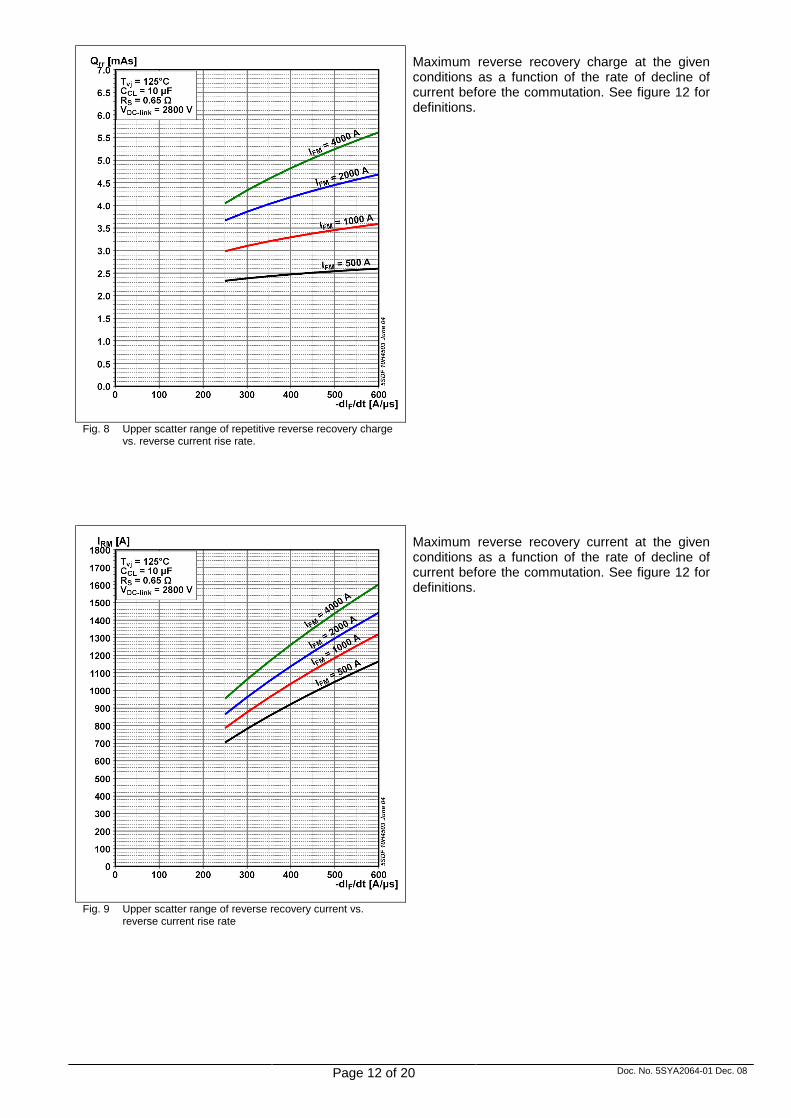
Maximum reverse recovery charge at the given conditions as a function of the rate of decline of current before the commutation. See figure 12 for definitions.
Fig. 8 Upper scatter range of repetitive reverse recovery charge vs. reverse current rise rate.
Maximum reverse recovery current at the given conditions as a function of the rate of decline of current before the commutation. See figure 12 for definitions.
Fig. 9 Upper scatter range of reverse recovery current vs. reverse current rise rate

Page 13 of 20 Doc. No. 5SYA2064-01 Dec. 08
Maximum turn-off switching energy depending on the on-state of the diode at the given conditions. The curve represents the upper scatter range of Err of the production distribution.
Fig. 10 Max. turn-off energy per pulse vs. on-state voltage.
Safe operating area at the given conditions. See figure 12 for definitions. Use of the diode outside these operation conditions could lead to catastrophic failures and should therefore be avoided.
Fig. 11 Diode Safe Operating Area

Page 14 of 20 Doc. No. 5SYA2064-01 Dec. 08
VFR
dIF/dt
IF (t)IF (t)
VF (t)
tfr
tfr (typ) 10 µs
Qrr
IRM
-dIF/dt
VF(t), IF (t)
VF (t)
VR (t)
t
Fig. 12 General current and voltage waveforms
LCLLi
RS
LLoadDUT
CCLVLC
IF
DCL
Electrical circuit used when determining the turn-on and turn-off data sheet ratings. CCL, DCL, RS and LCL represent the clamp circuit to limit switching over-voltages. LCL is a stray inductance and restricts the switching capability of the circuit. It should be designed as small as possible in an application.
The turn-off parameters Err and Qrr are only specified on the DUT position as a freewheeling diode. The reason is that on clamp position (DCL) turn-off losses are typically not the limiting criteria.
Fig. 13 Test circuit.
Fig. 14 Outline drawing, all dimensions are in millimeters and represent nominal values unless stated otherwise

Page 15 of 20 Doc. No. 5SYA2064-01 Dec. 08
Related documents: Doc. Nr. Titel 5SYA 2036 Recommendations regarding mechanical clamping of Press Pack High Power Semiconductors 5SYA 2061 Failure rates of fast recovery diodes due to cosmic rays 5SZK 9104 Specification of environmental class for pressure contact diodes, PCTs and GTO, STORAGE. Available on request,
please contact ABB’s Application Support. 5SZK 9105 Specification of environmental class for pressure contact diodes, PCTs and GTO, TRANSPORTATION. Available on
request, please contact ABB’s Application Support. Please refer to http://www.abb.com/semiconductors for current versions. A list of applicable documents is included at the end of the data sheet.
4 Design recommendations
4.1 Determine the right diode for standard application conditions
If the application conditions are close to the specified conditions in the datasheets of the used GTO or IGCT ABB recommends the use of the following diodes. If several diodes are recommended by ABB, the decision should be made according to the needs of the application:
• High expected losses in the diode -> use the larger diode • GTO/GCT and diodes in one combined -> use the diode with adequate mounting force
mechanical clamp system • Application conditions very close to the -> use the larger diode
GTO/IGCT SOA limits
GTO applications:
GTO Type Recommended freewheeling diodes
Recommended snubber diodes
5SDF 05D2505 5SGA 15F2502 5SDF 11F2501 5SDF 05D2501
5SDF 05D2505 5SGA 20H2501 5SDF 11F2501
5SDF 05D2501
5SDF 05D2505 5SGA 25H2501 5SDF 11F2501
5SDF 05D2501
5SGA 30J2501 5SDF 11F2501 5SDF 05D2501 5SGA 06D4502 5SDF 03D4501 5SDF 03D4501
5SDF 03D4501 5SGA 20H4502 5SDF 07F4501
5SDF 03D4501
5SDF 07F4501 5SGA 30J4502 5SDF 13H4501
5SDF 03D4501
5SDF 03D4501 5SGA 40L4501 5SDF 13H4501 5SDF 07H4501
5SDF 07F4501 5SDF 03D4501 5SGF 30J4502 5SDF 13H4501 5SDF 07H4501
5SDF 03D4501 5SGF 40L4502 5SDF 13H4501 5SDF 07H4501
Table 4: Recommended diodes for GTO applications

Page 16 of 20 Doc. No. 5SYA2064-01 Dec. 08
IGCT applications
IGCT Type Recommended freewheeling diodes
Recommended clamp diodes
Recommended NPC diodes**
5SHX 08F4510 Integrated 5SDF 03D4502 5SDF 03D4502 5SDF 03D4502
5SHX 14H4510 Integrated 5SDF 05F4502
5SDF 03D4502 5SDF 05F4502
5SDF 10H4503 5SDF 05F4502
5SHX 26L4510 Integrated 5SDF 10H4503
5SDF 03D4502 5SDF 05F4502 5SDF 10H4520
5SDF 02D6004 5SHX 06F6010 Integrated 5SDF 02D6004 5SDF 04F6004
5SDF 02D6004 5SDF 04F6004 5SHX 10H6010 Integrated 5SDF 04F6004 5SDF 08H6005 5SDF 02D6004 5SDF 04F6004 5SHX 19L6010 Integrated 5SDF 08H6005 5SDF 08H6005
5SHY 35L4510 5SHY 35L4511 5SHY 35L4512 5SHY 55L4500
5SDF 10H4503 5SDF 10H4520 5SDF 16L4503
5SDF 05F4502 5SDF 10H4503 5SDF 10H4520
5SDF 10H4503 5SDF 10H4520 5SDF 16L4503
Table 5: Recommended diodes for IGCT applications ** Note: NPC diodes stand for Neutral Point Clamp diodes. These diodes are typically used in 3-level inverters. The conditions to which these diodes are subjected are typically similar to the conditions of a freewheeling diode used in an IGCT inverter.
4.2 Determine the right diode for customized application conditions
If the application conditions differ from the specified conditions in the datasheet, the following parameters must be defined:
a) Diode type? Freewheeling diode, dv/dt at turn-off < 700V/µs GTO freewheeling diode Freewheeling diode, dv/dt at turn-off > 700V/µs IGCT diode Snubber diode in a GTO-application, no dc-blocking operation GTO snubber diode Clamp diode in an IGCT-application IGCT diode
b) Voltage class? Diodes with higher blocking voltage typically show
- Higher forward recovery during turn-on - Increased ruggedness and softness while turning off - Higher on-state and switching losses - Much lower cosmic radiation FIT rate at compared voltage. Please consider application
notes 5SYA2051 “Voltage ratings of high power semiconductors” and 5SYA2061 “Cosmic ray on FRD”
c) Diode-diameter?
Diodes with larger diameter show - Lower forward recovery during turn-on - Increased ruggedness - Lower on-state losses - Proportional to the silicon area higher cosmic radiation FIT rate at compared voltage - Lower thermal impedance - The need for higher clamping force. From a mechanical point of view it is often preferable to
clamp IGCT (GTO) und its related diodes in one single clamp system. If devices in one mechanical clamp have unequal pole-piece diameter, force spreaders have to be used. Please consider application note 5SYA2036 “Recommendations regarding mechanical clamping of Press Pack High Power Semiconductors”

Page 17 of 20 Doc. No. 5SYA2064-01 Dec. 08
4.3 Diode switching and important parameters to consider
4.3.1 Diode turn-on
During turn-on of a diode the two parameters turn-on energy (Eon) and peak forward recovery voltage (VFRM) are important to review regarding the specific needs of the application.
Fig. 15 shows the initial forward voltage overshoot VFRM, when a diode turns on with a high di/dt. VFRM is the peak voltage, and tfr characterizes the decay of the overshoot. The voltage overshoot originates from the fact that conductivity of the diode is initially reduced, because the number of free charge carriers available is much lower than in the steady-state. The device needs time to build up the required electron and hole concentration, within the bulk of the silicon. Measurements have shown that the VFRM vs. di/dt characteristic is slightly digressive. VFRM values at 125 °C are about double those at 25 °C. This behavior can be explained by reduced charge carrier mobility at elevated temperatures.
Fig. 15 Peak forward recovery voltage as a function of time Comparing VFRM values between diodes of different thickness, it is obvious that dynamic forward voltage increases exponentially with device thickness. This is explicable by the difficulty in achieving steady-state carrier concentration in a thick device within a few μs. Fig. 16 shows typical VFRM values relating to the active wafer area of ABB diodes. The red and orange curves belong to 6kV IGCT diodes and 5.5kV IGCT diodes at Tvj = 125°C, 80°C and 25°C while the blue colored curve is applicable for 4.5kV diodes at Tvj = 125°C. To estimate typical VFRM values of ABB diodes at a specific diF/dt the “di/dt per wafer area” of Fig. 16 has to be multiplied by the active wafer area of the diode. The active area of the different diodes correspond to the housing type which is listed in tables 1-3 where
D - housing corresponds to an active area of 24.3 cm2 F - housing corresponds to an active area of 33.8 cm2 H - housing corresponds to an active area of 46.3 cm2 L - housing corresponds to an active area of 65.2 cm2
Peak Forward Recovery Voltage = f (di/dt per wafer area) typical values
0
50
100
150
200
250
300
350
400
450
0 20 40 60 80 100 120
di/dt per wafer area [A / (us*cm2 )
V FR
M [V
]
6kV / 125°C6kV / 80°C6kV / 25°C4.5kV / 125°C
Fig. 16 Peak forward recovery voltage as a function of di/dt per wafer area

Page 18 of 20 Doc. No. 5SYA2064-01 Dec. 08
To estimate turn-on losses of a diode equation 2 can be taken to calculate the order of magnitude of Eon.
Eon_typ ≈ 1/6 * VFRM * diF/dt * tfr2 [Ws] Eqn 2
Where Eon_typ are the estimated typical turn-on losses, diF/dt is the applied turn-on di/dt, VFRM is the peak forward recovery voltage at diF/dt and tfr is the time constant of VFRM. Tfr depends on different parameter but can be chosen as 5µs for this raw calculation. Example 1: 5SDF 10H4503, 4.5 kV IGCT diode in L-housing on freewheeling position,
diF/dt = 600 A/µs, Tvj = 125°C
è di/dt per wafer area = 600 A/µs / 46.3 cm2 = 13 A/(µs*cm2) è VFRM ≈ 40 V è Eon_typ ≈ 1/6 * 40 V * 600 A/µs * 5µs2 = 0.1 Ws
Example 2: 5SDF 02D6004, 6 kV IGCT diode in D-housing on clamp position,
diF/dt = 2500 A/µs, Tvj = 125°C
è di/dt per wafer area = 2000 A/µs / 24.3 cm2 = 82 A/µs*cm2 è VFRM ≈ 350 V è Eon_typ ≈ 1/6 * 350 V * 2000 A/µs * 5µs2 = 2.9 Ws
It is obvious that turn-on losses of a diode on a freewheeling position are in most cases negligible since the diode typically has a large diameter and the diF/dt is in the range below 1000 A/µs. On a clamp position or on a snubber position the turn-on losses can become relevant. diF/dt is equal to the turn-off di/dt of the Switch (GTO or IGCT) and can be much higher than on a freewheeling position. Typical diF/dt that can be expected are in the range of the turn-off current of the switch per 1µs. E.g. turn-off of 3000A leads to a diF/dt in the range of 3000 A/µs. As a further effect VFRM of diodes on a GTO-snubber position or on an IGCT freewheeling- or clamp-position increases the dynamic commutation voltage of the Switch (GTO, IGCT with its freewheeling diode). This so called spike voltage VDSP is specified in the GTO and IGCT datasheets under “general current and voltage waveforms”. High values of this spike voltage reduce the switching capability of the switch. Because of this a larger snubber diode or IGCT diode increases the turn-off capability of the switch and vice versa. In terms of turn-off capability of the switch it is also recommended not to use too high voltage diodes. Typically snubber, clamp and freewheeling diodes are of the same voltage class as the related GTO or IGCT. It only makes sense to choose diodes of a higher voltage class if ruggedness in terms of turn-off switching of the diode itself is critical.

Page 19 of 20 Doc. No. 5SYA2064-01 Dec. 08
4.3.2 Diode turn-off Fig 17 shows the turn off of an IGCT diode on a freewheeling position. The forward current, IF, is switched off with a certain diF/dt (determined by the driving voltage and the di/dt limiting inductance), and continues to flow in the reverse direction until the pn junction is able to block reverse voltage. At this time, the reverse recovery current has reached its peak value IRM. The subsequent decay of the current and rise in reverse voltage are mainly determined by the diode itself and the applied voltage as a function of time. The applied voltage shape depends on the circuit of the application
Fig. 17 Turn-off of an IGCT freewheeling diode
It is the goal of the diode design engineer to ensure that the tail current decays in a “soft” manner, meaning without ringing or overshoot provoking “snap”, and that tail current and tail time are so small as to not contribute much to turn-off losses, despite reverse voltage being already high at this time. The application specific VR(t) is one of the main reasons that different diode designs are recommended for application conditions such as GTO-snubber diode, GTO-freewheeling diode or IGCT freewheeling- NPC- and clamp-diode. It is not recommended to use diodes above the maximum values specified in the data sheets. Especially the use of diodes in IGCT applications without dv/dt limitation is very sensitive regarding VDC-Link and LCL.
4.3.3 Surge current rating IFSM is the maximum allowed, non-repetitive and pulse-width dependent peak value of a half-sinusoidal surge current, applied at an instant when the diode is operating at its maximum junction temperature Tvjm. Although, in practice, the case temperature prior to a surge is always below Tvjm, both the junction and the housing are heated to Tvjm when the surge current limit is established. This worst-case test condition provides an additional margin to the real stress in an application. During a surge, the junction heats up to a temperature well above its rated maximum value. Therefore, the diode is no longer able to block rated voltage, so the IFSM values are valid only for VR = 0 V after the surge, i.e. without reapplied voltage. Although a single surge does not cause any irreversible damage to the silicon wafer, it should not be allowed to occur too frequently. I2t is an abbreviation and stands for ∫ IF2 dt. This value is derived from the IFSM value discussed above, according to equation 3:
2)(
2
0
22 pFSMt
F
tIdttItI
p ⋅== ∫ (for half-sinusoidal waveforms) [A2s] Eqn 3
To protect the diode, the I2t of a semiconductor fuse must be lower than the maximum I2t of the diode. The caveat for IFSM applies similarly to I2t. The shape of IFSM of applications depends on the protection concept and the electrical circuit and is therefore individual. The sinusoidal waveforms described in the datasheets typically don’t appear in applications with fast switching diodes. IFSM is a standardised value that enables comparison of datasheets of different devices and even of different manufacturers. When IFSM is expected to be close to the diode capability, ABB is able to simulate the stress that occurs under application conditions. As input data for the simulation i(t), starting values of Tcase and Tjunction and the mounting force Fm are needed. I(t) should be available in a numerical form such as ASCII or Excel.
I F (t)
Q rr
I RM
-dI F /dt
V
F (t), I F (t)
V F (t)
V R (t)
t

Page 20 of 20 Doc. No. 5SYA2064-01 Dec. 08
5 Additional notes
5.1 References
1) IEC 60747 “Semiconductor Devices”
2) 5SYA2036 “Recommendations regarding mechanical clamping of Press Pack High Power Semiconductors”
3) 5SYA2051 “Voltage ratings of high power semiconductors”
4) 5SYA2061 “Failure rates of fast recovery diodes due to cosmic rays”
5) 5SZK9104 “Specification of environmental class for pressure contact diodes, PCTs and GTO, STORAGE”
6) 5SZK9105 “Specification of environmental class for pressure contact diodes, PCTs and GTO, TRANSPORTATION”
The application notes, Reference 2 - 4, are available at www.abb.com/semiconductors
The environmental specifications 5 – 6 are available on request; please contact ABB’s Application Support
5.2 Application support
For further information please contact: Customer support: Raffael Schnell Phone +41 58 5861 366, fax +41 58 5861 306 e-mail [email protected] Address: ABB Switzerland Ltd Semiconductors Fabrikstrasse 3 CH-5600 Lenzburg Switzerland E-Mail [email protected] Internet www.abb.com/semiconductors Data sheets for the devices and your nearest sales office can be found on the ABB Switzerland Ltd, Semiconductors internet web site: http:// www.abb.com/semiconductors