Embed Size (px)
Citation preview

HD/SD SDI Receiver, with Integrated Adaptive Cable Equalizer complete with SMPTE Audio and Video Processing
GS1671
Key Features• Operation at 1.485Gb/s, 1.485/1.001Gb/s and 270Mb/s
• Supports SMPTE 292M, SMPTE 259M-C and DVB-ASI
• Integrated adaptive cable equalizer
• Typical equalized length of Belden 1694A cable:
230m at 1.485Gb/s
440m at 270Mb/s
• Integrated Reclocker with low phase noise, integrated VCO
• Serial digital reclocked, or non-reclocked output
• Integrated audio de-embedder for 8 channels of 48kHz audio
• Integrated audio clock generator
• Ancillary data extraction
• Parallel data bus selectable as either 20-bit or 10-bit
• Comprehensive error detection and correction features
• Output H, V, F or CEA 861 Timing Signals
• 1.2V digital core power supply, 1.2V and 3.3V analog power supplies, and selectable 1.8V or 3.3V I/O power supply
• GSPI Host Interface
• -20ºC to +85ºC operating temperature range
• Low power operation (typically 480mW)
• Small 11mm x 11mm 100-ball BGA package
• Pb-free and ROHS compliant
ErrataRefer to Errata document entitled GS1670/GS1671 Errata for this device (document number 53878).
Applications
Application: 1080p30 or 720p60 Monitor
AudioSelector
VideoProcessor
10-bit
HVF/PCLK
CTRL/TIMECODE
AES - OUT
AUDIO 1/2
Audio Clocks
Speakers
Display
DAC
DAC
HD-SDI GS1671
AUDIO 3/4
AUDIO 5/6
AUDIO 7/8
Application: Multi-format Downconverter
AudioProcessing
& Delay
GS4901
AnalogSync
SyncSeperator
10-bit
HVF/PCLK
HD/SDSerializer(GS1672)
VideoDownconverter &
Aspect RatioConversion
Memory
10-bit
10-bit bit SD Bypass
HVF/PCLK
Audio Clocks
AES 1/2
AES 3/4
AES 5/6
AES 7/8
HD/SD-SDISD/HD-SDI
GS1671
AES 1/2
AES 3/4
AES 5/6
AES 7/8
Application: Multi-input Video Monitoring System
GS4911
AnalogSync
SyncSeperator
VideoFormatter
VideoMemory
HVF/PCLK
Audio Clocks
10-bit
HVF/PCLK
AES OUT 1/2
AES OUT 3/4
AES OUT 5/6
AES OUT 7/8
HVF/PCLK
HVF/PCLK
AudioSelect
10-bit
10-bit
On ScreenDisplay
Generator
AES BUS AudioProcessor
HV/DE/PCLK
DVI/VGA DAC
VideoOutput
HD-SDIInput 1
GS1671
GS1671
GS1671
HD-SDIInput 2
HD-SDIInput n
1 of 130
GS1671 HD/SD SDI Integrated ReceiverData Sheet53737 - 2 September 2012
www.semtech.com

DescriptionThe GS1671 is a multi-rate SDI integrated Receiver which includes complete SMPTE processing, as per SMPTE 292M and SMPTE 259M-C. The SMPTE processing features can be bypassed to support signals with other coding schemes.
The GS1671 integrates Gennum's adaptive cable equalizer technology, achieving unprecedented cable lengths and jitter tolerance. It features DC restoration to compensate for the DC content of SMPTE pathological signals.
The device features an Integrated Reclocker with an internal VCO and a wide Input Jitter Tolerance (IJT) of 0.7UI.
A serial digital loop-through output is provided, which can be configured to output either reclocked or non-reclocked serial digital data. The serial digital output can be connected to an external cable driver.
The device operates in one of four basic modes: SMPTE mode, DVB-ASI mode, Data-Through mode or Standby mode.
In SMPTE mode (the default operating mode), the GS1671 performs full SMPTE processing, and features a number of data integrity checks and measurement capabilities.
The device also supports ancillary data extraction, and can provide entire ancillary data packets through host-accessible registers. It also provides a variety of other packet detection and error handling features. All of these processing features are optional, and may be individually enabled or disabled through register programming.
In DVB-ASI mode, sync word detection, alignment and 8b/10b decoding is applied to the received data stream.
In Data-Through mode all forms of SMPTE and DVB-ASI processing are disabled, and the device can be used as a simple serial to parallel converter.
The device can also operate in a lower power Standby mode. In this mode, no signal processing is carried out and the parallel output is held static.
Parallel data outputs are provided in 20-bit or 10-bit format for HD and SD video rates, with a variety of mapping options. As such, this parallel bus can interface directly with video processor ICs, and output data can be multiplexed onto 10 bits for a low pin count interface.
Up to eight channels (two audio groups) of serial digital audio may be extracted from the video data stream, in accordance with SMPTE 272M-C and SMPTE 299M.
The output audio formats supported by the device include AES/EBU and I2S, and two other industry standard serial digital formats. A variety of audio processing features are provided to ease implementation. Audio clocks are internally generated and provided by the device.
Application: Multi-format Audio De-embedder Module
PCLK
10-bit
GS1662
DAC
Switch Logic
&Drivers Analog
AudioOutputs
AESAudioOutputs
AUDIO 1/2
AUDIO 3/4
AUDIO 5/6
AUDIO 7/8
Audio Clocks
SD/HD-SDI GS1671
SD/HD-SDI
Application: Multi-format Digital VTR/Video Server
Storage:Tape/HDD/Solid State
AudioProcessor
VideoProcessor
10-bit
HVF/PCLK
Audio Outputs
V ideo Output
Audio Clocks
AUDIO 1/2
AUDIO 3/4
AUDIO 5/6
AUDIO 7/8
SD/HD-SDI GS1671
GS1671 HD/SD SDI Integrated ReceiverData Sheet53737 - 2 September 2012
2 of 130

Functional Block Diagram
GS1671 Functional Block Diagram
Buffer Mux
Reclockerwith
IntegratedVCO
SDI
SDO
SDO
Serialto
ParallelConverter
Descramble,Word Align,Rate Detect
FlywheelVideo
StandardDetect
TRSDetectTiming
Extraction
Mux
DVB-ASIDecoder
Illegal coderemap,
TRS/Line Number/
CRSInsertion,
EDH PacketInsertion
V/V
Sync
H/H
Sync
F/De
Rate_d
et[1:0]
ANC/Checksum
/352MExtraction
AudioDe-Embedder,Audio ClockGeneration
Error Flag
s
YA
NC
/CA
NC
LOC
KED
DV
B_A
SI
STA
ND
BY
GSPI andJTAG Controller
HostInterface
Output Mux/Demux
CrystalBuffer/
Oscillator
LFLB_CONT
VBG
RC
_BY
P
I/O Control
TIM
861
20B
IT/1
0BIT
SMPT
E_B
YPA
SSIO
PRO
C_E
N/D
IS
RES
ET_T
RST
CO
RE_
VD
DC
OR
E_G
ND
IO_V
DD
IO_G
ND
AU
DIO
_EN
/DIS
AO
UT_
1/2
AC
LKA
MC
LKW
CLK
SDO
_EN
/DIS
CS_
TMS
SCLK
_TC
LKSD
IN_T
DI
SDO
UT_
TDO
JTA
G/H
OST
XTA
L1
SW_E
N
VC
O_V
DD
VC
O_G
ND
PLL_
VD
DPL
L_G
ND
EQ_V
DD
EQ_G
ND
A_V
DD
A_G
ND
BU
FF_V
DD
BU
FF_G
ND
Buffer
SDI
AO
UT_
3/4
AO
UT_
5/6
AO
UT_
7/8
XTA
L2
XTA
L_O
UT
NGENEQ
AGC+AGC-
DOUT[19:0]
PCLK
LOCKED
GS1671 HD/SD SDI Integrated ReceiverData Sheet53737 - 2 September 2012
3 of 130
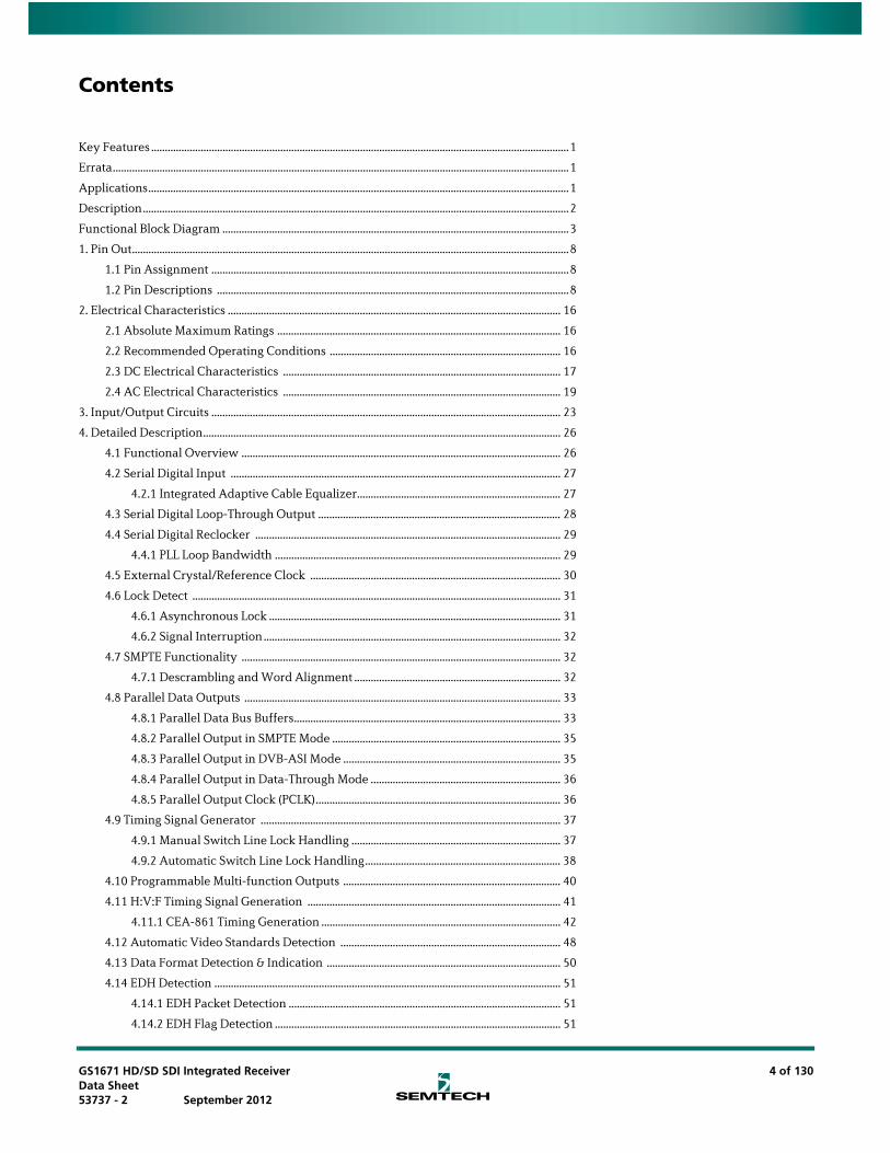
Contents
Key Features ........................................................................................................................................................1
Errata......................................................................................................................................................................1
Applications.........................................................................................................................................................1
Description...........................................................................................................................................................2
Functional Block Diagram ..............................................................................................................................3
1. Pin Out...............................................................................................................................................................8
1.1 Pin Assignment ..................................................................................................................................8
1.2 Pin Descriptions ................................................................................................................................8
2. Electrical Characteristics ......................................................................................................................... 16
2.1 Absolute Maximum Ratings ....................................................................................................... 16
2.2 Recommended Operating Conditions .................................................................................... 16
2.3 DC Electrical Characteristics ..................................................................................................... 17
2.4 AC Electrical Characteristics ..................................................................................................... 19
3. Input/Output Circuits ............................................................................................................................... 23
4. Detailed Description.................................................................................................................................. 26
4.1 Functional Overview .................................................................................................................... 26
4.2 Serial Digital Input ........................................................................................................................ 27
4.2.1 Integrated Adaptive Cable Equalizer.......................................................................... 27
4.3 Serial Digital Loop-Through Output ........................................................................................ 28
4.4 Serial Digital Reclocker ............................................................................................................... 29
4.4.1 PLL Loop Bandwidth ........................................................................................................ 29
4.5 External Crystal/Reference Clock ........................................................................................... 30
4.6 Lock Detect ...................................................................................................................................... 31
4.6.1 Asynchronous Lock .......................................................................................................... 31
4.6.2 Signal Interruption............................................................................................................ 32
4.7 SMPTE Functionality .................................................................................................................... 32
4.7.1 Descrambling and Word Alignment ........................................................................... 32
4.8 Parallel Data Outputs ................................................................................................................... 33
4.8.1 Parallel Data Bus Buffers................................................................................................. 33
4.8.2 Parallel Output in SMPTE Mode ................................................................................... 35
4.8.3 Parallel Output in DVB-ASI Mode ............................................................................... 35
4.8.4 Parallel Output in Data-Through Mode ..................................................................... 36
4.8.5 Parallel Output Clock (PCLK)......................................................................................... 36
4.9 Timing Signal Generator ............................................................................................................. 37
4.9.1 Manual Switch Line Lock Handling ............................................................................ 37
4.9.2 Automatic Switch Line Lock Handling....................................................................... 38
4.10 Programmable Multi-function Outputs ............................................................................... 40
4.11 H:V:F Timing Signal Generation ............................................................................................ 41
4.11.1 CEA-861 Timing Generation ....................................................................................... 42
4.12 Automatic Video Standards Detection ................................................................................ 48
4.13 Data Format Detection & Indication ..................................................................................... 50
4.14 EDH Detection .............................................................................................................................. 51
4.14.1 EDH Packet Detection ................................................................................................... 51
4.14.2 EDH Flag Detection ........................................................................................................ 51
GS1671 HD/SD SDI Integrated ReceiverData Sheet53737 - 2 September 2012
4 of 130

4.15 Video Signal Error Detection & Indication ......................................................................... 52
4.15.1 TRS Error Detection........................................................................................................ 54
4.15.2 Line Based CRC Error Detection ................................................................................ 54
4.15.3 EDH CRC Error Detection............................................................................................. 54
4.15.4 HD Line Number Error Detection .............................................................................. 55
4.16 Ancillary Data Detection & Indication ................................................................................. 55
4.16.1 Programmable Ancillary Data Detection................................................................ 56
4.16.2 SMPTE 352M Payload Identifier ................................................................................ 57
4.16.3 Ancillary Data Checksum Error ................................................................................. 57
4.16.4 Video Standard Error..................................................................................................... 58
4.17 Signal Processing ......................................................................................................................... 58
4.17.1 TRS Correction & Insertion........................................................................................... 59
4.17.2 Line Based CRC Correction & Insertion ................................................................... 59
4.17.3 Line Number Error Correction & Insertion ............................................................. 60
4.17.4 ANC Data Checksum Error Correction & Insertion ............................................. 60
4.17.5 EDH CRC Correction & Insertion ............................................................................... 60
4.17.6 Illegal Word Re-mapping ............................................................................................. 60
4.17.7 TRS and Ancillary Data Preamble Remapping...................................................... 61
4.17.8 Ancillary Data Extraction............................................................................................. 61
4.18 Audio De-embedder ................................................................................................................... 65
4.18.1 Serial Audio Data I/O Signals...................................................................................... 65
4.18.2 Serial Audio Data Format Support ............................................................................ 67
4.18.3 Audio Processing............................................................................................................. 71
4.18.4 Error Reporting ................................................................................................................ 77
4.19 GSPI - HOST Interface ................................................................................................................ 78
4.19.1 Command Word Description ...................................................................................... 78
4.19.2 Data Read or Write Access........................................................................................... 79
4.19.3 GSPI Timing....................................................................................................................... 80
4.20 Host Interface Register Maps .................................................................................................. 82
4.20.1 Video Core Registers...................................................................................................... 82
4.20.2 SD Audio Core Registers ............................................................................................... 91
4.20.3 HD Audio Core Registers............................................................................................ 106
4.21 JTAG Test Operation ................................................................................................................ 121
4.22 Device Power-up ....................................................................................................................... 123
4.23 Device Reset ................................................................................................................................ 123
4.24 Standby Mode ............................................................................................................................ 123
5. Application Reference Design ............................................................................................................. 124
5.1 High Gain Adaptive Cable Equalizers .................................................................................. 124
5.2 PCB Layout ..................................................................................................................................... 124
5.3 Typical Application Circuit ......................................................................................................125
6. References & Relevant Standards ....................................................................................................... 126
7. Package & Ordering Information ........................................................................................................ 127
7.1 Package Dimensions ................................................................................................................... 127
7.2 Packaging Data ............................................................................................................................. 128
7.3 Marking Diagram ......................................................................................................................... 128
7.4 Solder Reflow Profiles ................................................................................................................ 129
7.5 Ordering Information ................................................................................................................. 129
Revision History ............................................................................................................................................ 129
GS1671 HD/SD SDI Integrated ReceiverData Sheet53737 - 2 September 2012
5 of 130

List of Figures
Figure 3-1: Digital Input Pin with Schmitt Trigger............................................................................... 23Figure 3-2: Bidirectional Digital Input/Output Pin.............................................................................. 23Figure 3-3: Bidirectional Digital Input/Output Pin with programmable drive strength......... 24Figure 3-4: XTAL1/XTAL2/XTAL-OUT ................................................................................................... 24Figure 3-5: VBG .............................................................................................................................................. 24Figure 3-6: LB_CONT .................................................................................................................................... 25Figure 3-7: Loop Filter .................................................................................................................................. 25Figure 3-8: SDO/SDO .................................................................................................................................... 25Figure 3-9: Equalizer Input Equivalent Circuit .................................................................................... 25Figure 4-1: GS1671 Integrated EQ Block Diagram ............................................................................. 28Figure 4-2: 27MHz Clock Sources ............................................................................................................ 30Figure 4-3: PCLK to Data and Control Signal Output Timing - SDR Mode 1 .............................. 33Figure 4-4: PCLK to Data and Control Signal Output Timing - SDR Mode 2 .............................. 34Figure 4-5: Switch Line Locking on a Non-Standard Switch Line ................................................. 38Figure 4-6: H:V:F Output Timing - HDTV 20-bit Mode ..................................................................... 41Figure 4-7: H:V:F Output Timing - HDTV 10-bit Mode ..................................................................... 41Figure 4-8: H:V:F Output Timing - HD 20-bit Output Mode ............................................................ 42Figure 4-9: H:V:F Output Timing - HD 10-bit Output Mode ............................................................ 42Figure 4-10: H:V:F Output Timing - SD 20-bit Output Mode .......................................................... 42Figure 4-11: H:V:F Output Timing - SD 10-bit Output Mode .......................................................... 42Figure 4-12: H:V:DE Output Timing 1280 x 720p @ 59.94/60 (Format 4) ................................... 44Figure 4-13: H:V:DE Output Timing 1920 x 1080i @ 59.94/60 (Format 5) ................................. 44Figure 4-14: H:V:DE Output Timing 720 (1440) x 480i @ 59.94/60 (Format 6&7) .................... 45Figure 4-15: H:V:DE Output Timing 1280 x 720p @ 50 (Format 19) ............................................. 45Figure 4-16: H:V:DE Output Timing 1920 x 1080i @ 50 (Format 20) ........................................... 46Figure 4-17: H:V:DE Output Timing 720 (1440) x 576 @ 50 (Format 21 & 22) ........................... 46Figure 4-18: H:V:DE Output Timing 1920 x 1080p @ 23.94/24 (Format 32) .............................. 47Figure 4-19: H:V:DE Output Timing 1920 x 1080p @ 25 (Format 33) .......................................... 47Figure 4-20: H:V:DE Output Timing 1920 x 1080p @ 29.97/30 (Format 34) .............................. 48Figure 4-21: Y/1ANC and C/2ANC Signal Timing .............................................................................. 56Figure 4-22: Ancillary Data Extraction - Step A .................................................................................. 62Figure 4-23: Ancillary Data Extraction - Step B ................................................................................... 63Figure 4-24: Ancillary Data Extraction - Step C .................................................................................. 63Figure 4-25: Ancillary Data Extraction - Step D .................................................................................. 64Figure 4-26: ACLK to Data Signal Output Timing ............................................................................... 66Figure 4-27: I2S Audio Output Format .................................................................................................... 67Figure 4-28: AES/EBU Audio Output Format ....................................................................................... 67Figure 4-29: Serial Audio, Left Justified, MSB First ............................................................................. 68Figure 4-30: Serial Audio, Left Justified, LSB First .............................................................................. 68Figure 4-31: Serial Audio, Right Justified, MSB First .......................................................................... 68Figure 4-32: Serial Audio, Right Justified, LSB First ........................................................................... 68Figure 4-33: AES/EBU Audio Output to Bit Clock Timing ................................................................ 68Figure 4-34: ECC 24-bit Array and Examples ...................................................................................... 71Figure 4-35: Sample Distribution over 5 Video Frames (525-line Systems) ............................... 72Figure 4-36: Audio Buffer After Initial 26 Sample Write .................................................................. 73Figure 4-37: Audio Buffer Pointer Boundary Checking .................................................................... 73Figure 4-38: GSPI Application Interface Connection ........................................................................ 78Figure 4-39: Command Word Format ..................................................................................................... 78Figure 4-40: Data Word Format ................................................................................................................ 79Figure 4-41: Write Mode .............................................................................................................................. 80Figure 4-42: Read Mode ............................................................................................................................... 80
GS1671 HD/SD SDI Integrated ReceiverData Sheet53737 - 2 September 2012
6 of 130

Figure 4-43: GSPI Time Delay .................................................................................................................... 80Figure 4-44: In-Circuit JTAG .................................................................................................................... 122Figure 4-45: System JTAG ......................................................................................................................... 122Figure 4-46: Reset Pulse ............................................................................................................................. 123Figure 7-1: Pb-free Solder Reflow Profile ............................................................................................ 129
List of Tables
Table 1-1: Pin Descriptions ............................................................................................................................ 8Table 2-1: Absolute Maximum Ratings................................................................................................... 16Table 2-2: Recommended Operating Conditions................................................................................ 16Table 2-3: DC Electrical Characteristics ................................................................................................. 17Table 2-4: AC Electrical Characteristics ................................................................................................. 19Table 4-1: Serial Digital Output................................................................................................................. 28Table 4-2: PLL Loop Bandwidth ................................................................................................................ 29Table 4-3: Input Clock Requirements...................................................................................................... 30Table 4-4: Lock Detect Conditions............................................................................................................ 31Table 4-5: GS1671 Output Video Data Format Selections................................................................ 34Table 4-6: GS1671 PCLK Output Rates ................................................................................................... 36Table 4-7: Switch Line Position for Digital Systems ........................................................................... 39Table 4-8: Output Signals Available on Programmable Multi-Function Pins............................ 40Table 4-9: Supported CEA-861 Formats................................................................................................. 43Table 4-10: CEA861 Timing Formats ....................................................................................................... 43Table 4-11: Supported Video Standard Codes ..................................................................................... 48Table 4-12: Data Format Register Codes ................................................................................................ 50Table 4-13: Error Status Register and Error Mask Register .............................................................. 53Table 4-14: IOPROC_DISABLE Register Bits ......................................................................................... 59Table 4-15: Serial Audio Pin Descriptions ............................................................................................. 65Table 4-16: Audio Output Formats........................................................................................................... 67Table 4-17: Audio Data Packet Detect Register ................................................................................... 69Table 4-18: Audio Group DID Host Interface Settings....................................................................... 70Table 4-19: Audio Data and Control Packet DID Setting Register ................................................. 70Table 4-20: Audio Buffer Pointer Offset Settings ................................................................................ 74Table 4-21: Audio Channel Mapping Codes ......................................................................................... 74Table 4-22: Audio Sample Word Lengths .............................................................................................. 75Table 4-23: Audio Channel Status Information Registers ................................................................ 76Table 4-24: Audio Channel Status Block for Regenerate Mode Default Settings ..................... 76Table 4-25: Audio Mute Control Bits ....................................................................................................... 77Table 4-26: GSPI Time Delay...................................................................................................................... 80Table 4-27: GSPI Timing Parameters (50% levels; 3.3V or 1.8V operation) ................................ 81Table 4-28: Video Core Configuration and Status Registers............................................................ 82Table 4-29: SD Audio Core Configuration and Status Registers..................................................... 91Table 4-30: HD Audio Core Configuration and Status Registers.................................................. 106Table 4-31: ANC Extraction FIFO Access Registers.......................................................................... 121Table 7-1: Packaging Data......................................................................................................................... 128
GS1671 HD/SD SDI Integrated ReceiverData Sheet53737 - 2 September 2012
7 of 130

1. Pin Out
1.1 Pin Assignment
1.2 Pin Descriptions
1 32 4 5 6 7 8 9 10
A
B
C
D
E
F
G
H
J
K
PCLK
DVB_ASI
20bit/10bit
LF
SDO STANDBY
ACLK
JTAG/HOST
RESET_TRST
WCLK
A_VDD
CORE_GND
SDO
VBG
SDI
SDI
BUFF_VDD
SDO_EN/DIS
LB_CONTVCO_VDD
VCO_GND
RSVPLL_VDD
A_GND
A_GND
STAT0 STAT1
STAT2 STAT3
STAT4 STAT5
CORE_GND
CORE_GND
CORE_GND
CORE_VDD
CORE_VDD
CORE_VDD
CORE_VDD
DOUT1
DOUT0 DOUT2 DOUT3
DOUT4 DOUT5
DOUT6 DOUT7
DOUT8 DOUT9
DOUT10 DOUT11
DOUT14 DOUT13
DOUT16 DOUT15
DOUT18 DOUT17
DOUT19
DOUT12
IO_VDD
IO_GND
PLL_VDD
PLL_GND
PLL_VDD
A_GND
A_GND
A_GND
RC_BYP
SW_EN IO_GND IO_VDD
EQ_VDD EQ_GND PLL_GND
PLL_GND
AGCP RSV
SDOUT_TDO
CS_TMS
SDIN_TDI
SCLK_TCK
SMPTE_BYPASS
IO_GND IO_VDD
AUDIO_EN/DIS
AMCLK
AOUT_1/2
AOUT_3/4
AOUT_5/6
AOUT_7/8
TIM_861 XTAL_OUT
XTAL2
XTAL1
IO_GND
IO_VDD
IOPROC_EN/DIS
AGCN A_GND
BUFF_GND
CORE_GND
Table 1-1: Pin Descriptions
Pin Number
Name Timing Type Description
A1 VBG Analog Input Band Gap voltage filter connection.
A2 LF Analog Input Loop Filter component connection.
A3 LB_CONT Analog Input Connection for loop bandwidth control resistor.
A4 VCO_VDD Input Power POWER pin for the VCO. Connect to 1.2V±5% analog supply followed by a RC filter (see 5. Application Reference Design). A 105Ω 1% resistor must be used in the RC filter circuit. VCO_VDD is nominally 0.7V.
GS1671 HD/SD SDI Integrated ReceiverData Sheet53737 - 2 September 2012
8 of 130

A5, A6, B5, B6, C5, C6
STAT[0:5] Output MULTI-FUNCTIONAL OUTPUT PORT.
Please refer to the Output Logic parameters in the DC Electrical Characteristics table for logic level threshold and compatibility.
Each of the STAT [0:5] pins can be configured individually to output one of the following signals:
Signal
H/HSYNC V/VSYNC F/DE LOCKED Y/1ANC C/2ANC DATA ERROR VIDEO ERROR AUDIO ERROR EDH DETECTED CARRIER DETECT RATE_DET
Default
STAT0STAT1STAT2STAT3STAT4
−STAT5
−−−−−
A7, D10, G10, K7
IO_VDD Input Power POWER connection for digital I/O. Connect to 3.3V or 1.8V DC digital.
A8 PCLK Output PARALLEL DATA BUS CLOCK
Please refer to the Output Logic parameters in the DC Electrical Characteristics table for logic level threshold and compatibility.
HD 10-bit mode PCLK @ 148.5 or 148.5/1.001MHz
HD 20-bit mode PCLK @ 74.25 or 74.25/1.001MHz
SD 10-bit mode PCLK @ 27MHz
SD 20-bit mode PCLK @ 13.5MHz
Table 1-1: Pin Descriptions (Continued)
Pin Number
Name Timing Type Description
GS1671 HD/SD SDI Integrated ReceiverData Sheet53737 - 2 September 2012
9 of 130

A9, A10, B8, B9, B10,C8, C9, C10, E9,
E10
DOUT18, 17, 19, 16, 15, 12, 14, 13,
10, 11
Output PARALLEL DATA BUS
Please refer to the Output Logic parameters in the DC Electrical Characteristics table for logic level threshold and compatibility.
20-bit mode 20bit/10bit = HIGH
SMPTE mode (SMPTE_BYPASS = HIGH and DVB_ASI = LOW):
Luma data output for SD and HD data rates
DVB-ASI mode (SMPTE_BYPASS = LOW and DVB_ASI = HIGH):
Not defined
Data-Through mode (SMPTE_BYPASS = LOW and DVB_ASI = LOW):
Data output
10-bit mode 20bit/10bit = LOW
SMPTE mode (SMPTE_BYPASS = HIGH and DVB_ASI = LOW):
Multiplexed Luma/Chroma data output for SD and HD data rates
DVB-ASI mode (SMPTE_BYPASS = LOW and DVB_ASI = HIGH):
8b/10b decoded DVB-ASI data
Data-Through mode (SMPTE_BYPASS = LOW and DVB_ASI = LOW):
Data output
B1 A_VDD Input Power POWER pin for analog circuitry. Connect to 3.3V DC analog.
B2, C3, C4 PLL_VDD Input Power POWER pins for the Reclocker PLL. Connect to 1.2V DC analog.
B3, F2 RSV These pins must be left unconnected.
B4 VCO_GND Input Power GND pin for the VCO. Connect to analog GND.
B7, D9, G9, J7
IO_GND Input Power GND connection for digital I/O. Connect to digital GND.
C1, D1 SDI, SDI Analog Input Serial Digital Differential Input.
C2, D2, D3, E3, F3, G2
A_GND Input Power GND pins for sensitive analog circuitry. Connect to analog GND.
C7 RESET_TRST Input CONTROL SIGNAL INPUT
Please refer to the Input Logic parameters in the DC Electrical Characteristics table for logic level threshold and compatibility.
Used to reset the internal operating conditions to default settings and to reset the JTAG sequence.
Normal mode (JTAG/HOST = LOW):
When LOW, all functional blocks are set to default conditions and all digital output signals become high impedance.
When HIGH, normal operation of the device resumes.
JTAG test mode (JTAG/HOST = HIGH):
When LOW, all functional blocks are set to default and the JTAG test sequence is reset.
When HIGH, normal operation of the JTAG test sequence resumes after RESET_TRST is de-asserted.
D4, E4, F4 PLL_GND Input Power GND pins for the Reclocker PLL. Connect to analog GND.
Table 1-1: Pin Descriptions (Continued)
Pin Number
Name Timing Type Description
GS1671 HD/SD SDI Integrated ReceiverData Sheet53737 - 2 September 2012
10 of 130

D5, E5, F5, G4, G5
CORE_GND Input Power GND connection for device core. Connect to digital GND.
D6, E6, F6, G6
CORE_VDD Input Power POWER connection for device core. Connect to 1.2V DC digital.
D7 SW_EN Input CONTROL SIGNAL INPUT
Please refer to the Input Logic parameters in the DC Electrical Characteristics table for logic level threshold and compatibility.
Used to enable switch-line locking, as described in Section 4.9.1.
D8 JTAG/HOST Input CONTROL SIGNAL INPUT
Please refer to the Input Logic parameters in the DC Electrical Characteristics table for logic level threshold and compatibility.
Used to select JTAG test mode or host interface mode.
When JTAG/HOST is HIGH, the host interface port is configured for JTAG test.
When JTAG/HOST is LOW, normal operation of the host interface port resumes.
E1 EQ_VDD Input Power POWER pin for SDI buffer. Connect to 3.3V DC analog.
E2 EQ_GND Input Power GND pin for SDI buffer. Connect to analog GND.
E7 SDOUT_TDO Output COMMUNICATION SIGNAL OUTPUT
Please refer to the Output Logic parameters in the DC Electrical Characteristics table for logic level threshold and compatibility.
GSPI serial data output/test data out.
In JTAG mode (JTAG/HOST = HIGH), this pin is used to shift test results from the device.
In host interface mode, this pin is used to read status and configuration data from the device.
Note: GSPI is slightly different than the SPI. For more details on GSPI, please refer to 4.19 GSPI - HOST Interface.
E8 SDIN_TDI Input COMMUNICATION SIGNAL INPUT
Please refer to the Input Logic parameters in the DC Electrical Characteristics table for logic level threshold and compatibility.
GSPI serial data in/test data in.
In JTAG mode (JTAG/HOST = HIGH), this pin is used to shift test data into the device.
In host interface mode, this pin is used to write address and configuration data words into the device.
F1, G1 AGCP, AGCN Automatic Gain Control for the equalizer. Attach the AGC capacitor between these pins.
Table 1-1: Pin Descriptions (Continued)
Pin Number
Name Timing Type Description
GS1671 HD/SD SDI Integrated ReceiverData Sheet53737 - 2 September 2012
11 of 130

F7 CS_TMS Input COMMUNICATION SIGNAL INPUT
Please refer to the Input Logic parameters in the DC Electrical Characteristics table for logic level threshold and compatibility.
Chip select / test mode start.
In JTAG mode (JTAG/HOST = HIGH), this pin is Test Mode Start, used to control the operation of the JTAG test.
In host interface mode (JTAG/HOST = LOW), this pin operates as the host interface chip select and is active LOW.
F8 SCLK_TCK Input COMMUNICATION SIGNAL INPUT
Please refer to the Input Logic parameters in the DC Electrical Characteristics table for logic level threshold and compatibility.
Serial data clock signal.
In JTAG mode (JTAG/HOST = HIGH), this pin is the JTAG clock.
In host interface mode (JTAG/HOST = LOW), this pin is the host interface serial bit clock.
All JTAG/host interface addresses and data are shifted into/out of the device synchronously with this clock.
F9, F10, H9, H10, J8, J9, J10, K8, K9,
K10
DOUT8, 9, 6, 7, 1, 4, 5, 0, 2, 3
Output PARALLEL DATA BUS
Please refer to the Output Logic parameters in the DC Electrical Characteristics table for logic level threshold and compatibility.
20-bit mode 20bit/10bit = HIGH
SMPTE mode (SMPTE_BYPASS = HIGH and DVB_ASI = LOW):
Chroma data output for SD and HD data rates
DVB-ASI mode (SMPTE_BYPASS = LOW and DVB_ASI = HIGH):
Not defined
Data-Through mode (SMPTE_BYPASS = LOW and DVB_ASI = LOW):
Data output
10-bit mode 20bit/10bit = LOW
Forced LOW
G3 RC_BYP Input CONTROL SIGNAL INPUT
Please refer to the Input Logic parameters in the DC Electrical Characteristics table for logic level threshold and compatibility.
When this pin is LOW, the serial digital output is the buffered version of the input serial data. When this pin is HIGH, the serial digital output is the reclocked version of the input serial data.
Table 1-1: Pin Descriptions (Continued)
Pin Number
Name Timing Type Description
GS1671 HD/SD SDI Integrated ReceiverData Sheet53737 - 2 September 2012
12 of 130

G7 SMPTE_BYPASS Input/Output CONTROL SIGNAL INPUT/OUTPUT
Please refer to the Input/Output Logic parameters in the DC Electrical Characteristics table for logic level threshold and compatibility.
Indicates the presence of valid SMPTE data.
When the AUTO/MAN bit in the host interface register is HIGH (Default), this pin is an OUTPUT. SMPTE_BYPASS is HIGH when the device locks to a SMPTE compliant input. SMPTE_BYPASS is LOW under all other conditions.
When the AUTO/MAN bit in the host interface register is LOW, this pin is an INPUT:
No SMPTE scrambling takes place, and none of the I/O processing features of the device are available when SMPTE_BYPASS is set LOW.
When SMPTE_BYPASS is set HIGH, the device carries out SMPTE scrambling and I/O processing.
When SMPTE_BYPASS and DVB_ASI are both set LOW, the device operates in Data-Through mode.
G8 DVB_ASI Input/Output CONTROL SIGNAL INPUT
Please refer to the Input/Output Logic parameters in the DC Electrical Characteristics table for logic level threshold and compatibility.
Used to enable/disable DVB-ASI data extraction in manual mode.
When the AUTO/MAN bit in the host interface is LOW, this pin is an input and when the DVB_ASI pin is set HIGH the device will carry out DVB_ASI data extraction and processing. The SMPTE_BYPASS pin must be set LOW. When SMPTE_BYPASS and DVB_ASI are both set LOW, the device operates in Data-Through mode.
When the AUTO/MAN bit in the host interface is HIGH (default), DVB-ASI is configured as a status output (set LOW), and DVB-ASI input streams are not supported or recognized.
H1 BUFF_VDD Input Power POWER pin for the serial digital output 50Ω buffer. Connect to 3.3V DC analog.
H2 BUFF_GND Input Power GND pin for the cable driver buffer. Connect to analog GND.
H3 AUDIO_EN/DIS Input CONTROL SIGNAL INPUT
Please refer to the Input Logic parameters in the DC Electrical Characteristics table for logic level threshold and compatibility.
Enables or disables audio extraction.
H4 WCLK Output 48kHz word clock for Audio.
Please refer to the Output Logic parameters in the DC Electrical Characteristics table for logic level threshold and compatibility.
H5 TIM_861 Input CONTROL SIGNAL INPUT
Please refer to the Input Logic parameters in the DC Electrical Characteristics table for logic level threshold and compatibility.
Used to select CEA-861 timing mode.
When TIM_861 is HIGH, the device outputs CEA 861 timing signals (HSYNC/VSYNC/DE) instead of H:V:F digital timing signals.
H6 XTAL_OUT Digital Output
Buffered 27MHz crystal output. Can be used to cascade the crystal signal.
Table 1-1: Pin Descriptions (Continued)
Pin Number
Name Timing Type Description
GS1671 HD/SD SDI Integrated ReceiverData Sheet53737 - 2 September 2012
13 of 130

H7 20bit/10bit Input CONTROL SIGNAL INPUT
Please refer to the Input Logic parameters in the DC Electrical Characteristics table for logic level threshold and compatibility.
Used to select the output bus width.
HIGH = 20-bit, LOW = 10-bit.
H8 IOPROC_EN/DIS Input CONTROL SIGNAL INPUT
Please refer to the Input Logic parameters in the DC Electrical Characteristics table for logic level threshold and compatibility.
Used to enable or disable audio and video processing features. When IOPROC_EN is HIGH, the audio and video processing features of the device are enabled. When IOPROC_EN is LOW, the processing features of the device are disabled, and the device is in a low-latency operating mode.
J1, K1 SDO, SDO Output Serial Data Output Signal.
50Ω CML buffer for interfacing to an external cable driver.
Serial digital output signal operating at 1.485Gb/s, 1.485/1.001Gb/s and 270Mb/s.
J2 SDO_EN/DIS Input CONTROL SIGNAL INPUT
Please refer to the Input Logic parameters in the DC Electrical Characteristics table for logic level threshold and compatibility.
Used to enable/disable the serial digital output stage.
When SDO_EN/DIS is LOW, the serial digital output signals, SDO and SDO, are both pulled HIGH.
When SDO_EN/DIS is HIGH, the serial digital output signals, SDO and SDO, are enabled.
J3 AOUT_1/2 Output Serial Audio Output; Channels 1 and 2.
Please refer to the Output Logic parameters in the DC Electrical Characteristics table for logic level threshold and compatibility.
J4 ACLK Output 64fs sample clock for audio.
Please refer to the Output Logic parameters in the DC Electrical Characteristics table for logic level threshold and compatibility.
J5 AOUT_5/6 Output Serial Audio Output; Channels 5 and 6.
Please refer to the Output Logic parameters in the DC Electrical Characteristics table for logic level threshold and compatibility.
J6, K6 XTAL2, XTAL1 Analog Input Input connection for 27MHz crystal.
K2 STANDBY Input CONTROL SIGNAL INPUT
Please refer to the Input Logic parameters in the DC Electrical Characteristics table for logic level threshold and compatibility.
When this pin is set HIGH, the device is placed in a power-saving mode. No data processing occurs, and the digital I/Os are powered down.
In this mode, the serial digital output signals, SDO and SDO, are both pulled HIGH.
K3 AOUT_3/4 Output Serial Audio Output; Channels 3 and 4.
Please refer to the Output Logic parameters in the DC Electrical Characteristics table for logic level threshold and compatibility.
Table 1-1: Pin Descriptions (Continued)
Pin Number
Name Timing Type Description
GS1671 HD/SD SDI Integrated ReceiverData Sheet53737 - 2 September 2012
14 of 130

K4 AMCLK Output Oversampled master clock for audio (128fs, 256fs, 512fs selectable).
Please refer to the Output Logic parameters in the DC Electrical Characteristics table for logic level threshold and compatibility.
K5 AOUT_7/8 Output Serial Audio Output; Channels 7 and 8.
Please refer to the Output Logic parameters in the DC Electrical Characteristics table for logic level threshold and compatibility.
Table 1-1: Pin Descriptions (Continued)
Pin Number
Name Timing Type Description
GS1671 HD/SD SDI Integrated ReceiverData Sheet53737 - 2 September 2012
15 of 130

2. Electrical Characteristics
2.1 Absolute Maximum Ratings
2.2 Recommended Operating Conditions
Table 2-1: Absolute Maximum Ratings
Parameter Value/Units
Supply Voltage, Digital Core (CORE_VDD) -0.3V to +1.5V
Supply Voltage, Digital I/O (IO_VDD) -0.3V to +4.0V
Supply Voltage, Analog 1.2V (PD_VDD, VCO_VDD) -0.3V to +1.5V
Supply Voltage, Analog 3.3V (EQ_VDD, BUFF_VDD, A_VDD)
-0.3V to +4.0V
Input Voltage Range (digital inputs) -2.0V to +5.25V
Ambient Operating Temperature (TA) -40°C < TA < 95°C
Storage Temperature (TSTG) -40°C < TSTG < 125°C
Peak Reflow Temperature (JEDEC J-STD-020C) 260°C
ESD Sensitivity, HBM (JESD22-A114) 2kV
NOTES:
Absolute Maximum Ratings are those values beyond which damage may occur. Functional operation under these conditions or at any other condition beyond those indicated in the AC/DC Electrical Characteristics sections is not implied.
Table 2-2: Recommended Operating Conditions
Parameter Symbol Conditions Min Typ Max Units Notes
Operating Temperature Range, Ambient
TA – -20 − 85 °C −
Supply Voltage, Digital Core CORE_VDD – 1.14 1.2 1.26 V −
Supply Voltage, Digital I/O IO_VDD1.8V mode 1.71 1.8 1.89 V −
3.3V mode 3.13 3.3 3.47 V −
Supply Voltage, PLL PLL_VDD – 1.14 1.2 1.26 V –
Supply Voltage, VCO VCO_VDD – − 0.7 − V 1
Supply Voltage, Analog A_VDD – 3.13 3.3 3.47 V 2
Supply Voltage, Serial Digital Input EQ_VDD – 3.13 3.3 3.47 V 2
Supply Voltage, CD Buffer BUFF_VDD – 3.13 3.3 3.47 V 2
NOTES
1. This is 0.7V rather than 1.2V because there is a voltage drop across an external 105Ω resistor. See Typical Application Circuit on page 125.2. The 3.3V supplies must track the 3.3V supply of an external CD.
GS1671 HD/SD SDI Integrated ReceiverData Sheet53737 - 2 September 2012
16 of 130

2.3 DC Electrical Characteristics
Table 2-3: DC Electrical Characteristics
Guaranteed over recommended operating conditions unless otherwise noted.
Parameter Symbol Conditions Min Typ Max Units Notes
System
+1.2V Supply Current I1V2 10/20bit HD − 170 220 mA −
10/20bit SD − 140 185 mA −
DVB_ASI − 130 170 mA −
+1.8V Supply Current I1V8 10/20bit HD − 15 21 mA −
10/20bit SD − 4 7 mA −
DVB_ASI − 4 6 mA −
+3.3V Supply Current I3V3 10/20bit HD − 110 135 mA −
10/20bit SD − 90 100 mA −
DVB_ASI − 90 95 mA −
Total Device Power (IO_VDD = 1.8V)
P1D8 10/20bit HD − 480 590 mW −
10/20bit SD − 420 520 mW −
DVB_ASI − 410 500 mW −
Reset − 390 − mW −
Standby − 23 45 mW −
Total Device Power (IO_VDD = 3.3V)
P3D3 10/20bit HD − 570 730 mW −
10/20bit SD − 460 560 mW −
DVB_ASI − 440 540 mW −
Reset − 410 − mW −
Standby − 23 45 mW −
Digital I/O
Input Logic LOW VIL 3.3V or 1.8V operationIO_VSS
-0.3–
0.3 x IO_VDD
V –
Input Logic HIGH VIH 3.3V or 1.8V operation0.7 x
IO_VDD–
IO_VDD+0.3
V –
Output Logic LOW VOLIOL = 5mA, 1.8V operation – – 0.2 V –
IOL = 8mA, 3.3V operation – – 0.4 V –
Output Logic HIGH VOHIOH = 5mA, 1.8V operation 1.4 – – V –
IOH = 8mA, 3.3V operation 2.4 – – V –
Serial Input
Serial Input Common Mode Voltage
– 75Ω load – 2.2 – V –
Serial Output
Serial Output Common Mode Voltage
− 50Ω load BUFF_VDD-(0.6/2)
BUFF_VDD-(0.45/2)
BUFF_VDD-(0.35/2)
V −
GS1671 HD/SD SDI Integrated ReceiverData Sheet53737 - 2 September 2012
17 of 130

Notes:
The output drive strength of the digital outputs can be programmed through the host interface. please see Table 4-28: Video Core Configuration and Status Registers, register 06Dh for details.
Table 2-3: DC Electrical Characteristics (Continued)
Guaranteed over recommended operating conditions unless otherwise noted.
Parameter Symbol Conditions Min Typ Max Units Notes
GS1671 HD/SD SDI Integrated ReceiverData Sheet53737 - 2 September 2012
18 of 130

2.4 AC Electrical Characteristics
Table 2-4: AC Electrical Characteristics
Guaranteed over recommended operating conditions unless otherwise noted.
Parameter Symbol Conditions Min Typ Max Units Notes
System
Device Latency:
AUDIO_EN = 1,
SMPTE mode,
IOPROC_EN = 1
–
HD 79 – 83 PCLK –
SD 50 – 59 PCLK –
Device Latency:
AUDIO_EN = 0,
SMPTE mode,
IOPROC_EN = 1
–
HD 44 – 48 PCLK –
SD 44 – 48 PCLK –
Device Latency:
AUDIO_EN = 0, SMPTE mode, IOPROC_EN = 0
–
HD 33 – 36 PCLK –
SD 32 – 35 PCLK –
Device Latency:
AUDIO_EN = 0, SMPTE bypass, IOPROC_EN = 0
–
HD 6 – 9 PCLK –
SD 5 – 9 PCLK –
Device Latency:
DVB-ASI– SD 12 – 16 PCLK –
Reset Pulse Width treset – 1 – – ms –
Parallel Output
Parallel Clock Frequency fPCLK – 13.5 – 148.5 MHz –
Parallel Clock Duty Cycle DCPCLK – 40 – 60 % –
Output Data Hold Time (1.8V) toh HD 10-bit6pF Cload
DBUS 1.0 – – ns 1
STAT 1.0 – – ns 1
HD 20-bit6pF Cload
DBUS 1.0 – – ns 1
STAT 1.0 – – ns 1
SD 10-bit6pF Cload
DBUS 19.4 – – ns 1
STAT 19.4 – – ns 1
SD 20-bit6pF Cload
DBUS 38.0 – – ns 1
STAT 38.0 – – ns 1
GS1671 HD/SD SDI Integrated ReceiverData Sheet53737 - 2 September 2012
19 of 130

Output Data Hold Time (3.3V) toh HD 10-bit6pF Cload
DBUS 1.0 – – ns 2
STAT 1.0 – – ns 2
HD 20-bit6pF Cload
DBUS 1.0 – – ns 2
STAT 1.0 – – ns 2
SD 10-bit6pF Cload
DBUS 19.4 – – ns 2
STAT 19.4 – – ns 2
SD 20-bit6pF Cload
DBUS 38.0 – – ns 2
STAT 38.0 – – ns 2
Output Data Delay Time (1.8V) tod HD 10-bit15pF Cload
DBUS – – 3.7 ns 3
STAT – – 4.4 ns 3
HD 20-bit15pF Cload
DBUS – – 3.7 ns 3
STAT – – 4.4 ns 3
SD 10-bit15pF Cload
DBUS – – 22.2 ns 3
STAT – – 22.2 ns 3
SD 20-bit15pF Cload
DBUS – – 41.0 ns 3
STAT – – 41.0 ns 3
Output Data Delay Time (3.3V) tod HD 10-bit15pF Cload
DBUS – – 3.7 ns 4
STAT – – 4.1 ns 4
HD 20-bit15pF Cload
DBUS – – 3.7 ns 4
STAT – – 4.1 ns 4
SD 10-bit15pF Cload
DBUS – – 22.2 ns 4
STAT – – 22.2 ns 4
SD 20-bit15pF Cload
DBUS – – 41.0 ns 4
STAT – – 41.0 ns 4
Output Data Rise/Fall Time (1.8V) tr/tf All modes6pF Cload
STAT – – 0.4 ns 1
DBUS – – 0.4 ns 1
AUDIO – – 0.6 ns 1
All modes15pF Cload
STAT – – 1.5 ns 3
DBUS – – 1.4 ns 3
AUDIO – – 2.3 ns 3
Table 2-4: AC Electrical Characteristics (Continued)
Guaranteed over recommended operating conditions unless otherwise noted.
Parameter Symbol Conditions Min Typ Max Units Notes
GS1671 HD/SD SDI Integrated ReceiverData Sheet53737 - 2 September 2012
20 of 130

Output Data Rise/Fall Time (3.3V) tr/tf All modes6pF Cload
STAT – – 0.5 ns 2
DBUS – – 0.4 ns 2
AUDIO – – 0.6 ns 2
All modes15pF Cload
STAT – – 1.6 ns 4
DBUS – – 1.4 ns 4
AUDIO – – 2.2 ns 4
Serial Digital Input
Serial Input Data Rate DRSDI – 0.27 – 1.485 Gb/s –
Serial Input Voltage Swing ΔVSDI TA =25°C, differential, 270Mb/s & 1.485Gb/s
720 800 950 mVp-p 6
Achievable Cable Length –Belden 1694A cable, HD 210 230 – m –
Belden 1694A cable, SD 400 440 – m –
Input Return Loss – single ended 15 21 – dB 7
Input Resistance – single ended – 1.52 – kΩ –
Input Capacitance – single ended – 1 – pF –
Serial Digital Output
Serial Output Data Rate DRSDO – 0.27 – 1.485 Gb/s –
Serial Output SwingΔVSDO Differential with 100Ω
load320 – 600 mVp-p –
Serial Output Rise Time 20% ~ 80%
trSDO –– – 180 ps –
Serial Output Fall Time 20% ~ 80%
tfSDO – – – 180 ps –
Serial Output Jitter with loop-through mode
tOJ HD, PRBS23, Belden 1694A cable, 210m
– – 100 ps –
SD, PRBS23, Belden 1694A cable, 440m
– – 470 ps –
Serial Output Duty Cycle Distortion
DCDSDD HD – 10 – ps –
SD – 20 – ps –
Synchronous lock time – – – – 25 μs –
Asynchronous lock time – – 0.1 – 20 ms –
Lock time from power-up – After 20 minutes at -20°C
– – 5 s –
Table 2-4: AC Electrical Characteristics (Continued)
Guaranteed over recommended operating conditions unless otherwise noted.
Parameter Symbol Conditions Min Typ Max Units Notes
GS1671 HD/SD SDI Integrated ReceiverData Sheet53737 - 2 September 2012
21 of 130

GSPI
GSPI Input Clock Frequency fSCLK 50% levels3.3V or 1.8V operation
– – 60 MHz 5
GSPI Input Clock Duty Cycle DCSCLK 40 50 60 % 5
GSPI Input Data Setup Time – 1.5 – – ns 5
GSPI Input Data Hold Time – 1.5 – – ns 5
GSPI Output Data Hold Time – – 1.5 – – ns 5
CS low before SCLK rising edge – 50% levels3.3V or 1.8V operation
1.5 – – ns 5
Time between end of command word (or data in Auto-Increment mode) and the first SCLK of the following data word - write cycle
– 50% levels3.3V or 1.8V operation
37.1 – – ns 5
Time between end of command word (or data in Auto-Increment mode) and the first SCLK of the following data word - read cycle
– 50% levels3.3V or 1.8V operation
148.4 – – ns 5
CS high after SCLK falling edge – 50% levels3.3V or 1.8V operation
37.1 – – ns 5
Notes:
1. 1.89V and 0ºC.2. 3.47V and 0ºC.3. 1.71V and 85ºC4. 3.13V and 85ºC5. Timing parameters defined in Section 4.19.36. 0m cable length7. Tested on a GS1671 board from 5MHz to 1.485GHz.
Table 2-4: AC Electrical Characteristics (Continued)
Guaranteed over recommended operating conditions unless otherwise noted.
Parameter Symbol Conditions Min Typ Max Units Notes
GS1671 HD/SD SDI Integrated ReceiverData Sheet53737 - 2 September 2012
22 of 130

3. Input/Output Circuits
Figure 3-1: Digital Input Pin with Schmitt Trigger (20BIT/10BIT, AUDIO_EN/DIS, CS_TMS, SW_EN, IOPROC_EN/DIS, JTAG/HOST, RC_BYP, RESET_TRST, SCLK_TCK, SDIN_TDI, SDO_EN/DIS, STANDBY, TIM_861)
Figure 3-2: Bidirectional Digital Input/Output Pin - Configured to Output unless in Reset Mode. (ACLK, AMCLK, AOUT_1/2, AOUT_3/4, AOUT_5/6, AOUT_7/8, DVB_ASI, SMPTE_BYPASS, WCLK)
IO_VDD
200Ω
Input Pin
IO_VDD
200Ω
Output Pin
GS1671 HD/SD SDI Integrated ReceiverData Sheet53737 - 2 September 2012
23 of 130

Figure 3-3: Bidirectional Digital Input/Output Pin with programmable drive strength. These pins are configured to output unless in Reset Mode; in which case they are high-impedance. The drive strength can be set by writing to address 06Dh in the host interface register. (DOUT0, DOUT1, DOUT2, DOUT3, DOUT4, DOUT5, DOUT6, DOUT7, DOUT8, DOUT9, SDOUT_TDO, STAT0, STAT1, STAT2, STAT3, STAT4, STAT5, XTAL_OUT, DOUT10, DOUT11, DOUT12, DOUT13, DOUT14, DOUT15, DOUT16, DOUT17, DOUT18, DOUT19, PCLK)
Figure 3-4: XTAL1/XTAL2/XTAL-OUT
Figure 3-5: VBG
IO_VDD
200Ω
Output Pin
XTAL1
XTAL2
XTAL_OUT
VBG50Ω
2kΩ
A_VDD
GS1671 HD/SD SDI Integrated ReceiverData Sheet53737 - 2 September 2012
24 of 130

Figure 3-6: LB_CONT
Figure 3-7: Loop Filter
Figure 3-8: SDO/SDO
Figure 3-9: Equalizer Input Equivalent Circuit
Out <0>
Out <1>
EQ_VDD
LB_CONT
25Ω
PLL_VDD
LF
25Ω
50Ω 50Ω
SDO
SDO
BUFF_VDD
4k
6k
4k
6kRC
SDI SDI
GS1671 HD/SD SDI Integrated ReceiverData Sheet53737 - 2 September 2012
25 of 130

4. Detailed Description
Refer to the document entitled GS1670/GS1671 Errata for this device (document number 53878).
4.1 Functional OverviewThe GS1671 is a multi-rate SDI integrated Receiver which includes complete SMPTE processing, as per SMPTE 292M and SMPTE 259M-C. The SMPTE processing features can be bypassed to support signals with other coding schemes.
The GS1671 integrates Gennum's adaptive cable equalizer technology, achieving unprecedented cable lengths and jitter tolerance. It features DC restoration to compensate for the DC content of SMPTE pathological signals.
The device features an Integrated Reclocker with an internal VCO and a wide Input Jitter Tolerance (IJT) of 0.7UI.
A serial digital loop through output is provided, which can be configured to output either reclocked or non-reclocked serial digital data. The Serial Digital Output can be connected to an external Cable Driver.
The device operates in one of four basic modes: SMPTE mode, DVB-ASI mode, Data-Through mode or Standby mode.
In SMPTE mode, the GS1671 performs SMPTE de-scrambling and NRZI to NRZ decoding and word alignment. Line-based CRC errors, line number errors, TRS errors and ancillary data check sum errors can all be detected. The GS1671 also provides ancillary data extraction. The entire ancillary data packet is extracted, and written to host-accessible registers. Other processing functions include H:V:F timing extraction, Luma and Chroma ancillary data indication, video standard detection, and SMPTE 352M packet detection and decoding. All of the processing features are optional, and may be enabled or disabled via the Host Interface.
In DVB-ASI mode, 8b/10b decoding is applied to the received data stream.
In Data-Through mode, all forms of SMPTE and DVB-ASI decoding are disabled, and the device can be used as a simple serial to parallel converter.
The device can also be placed in a lower power Standby mode. In this mode, no signal processing is carried out and the parallel output is held static. Placing the Receiver in Standby mode will automatically place the integrated equalizer in power down mode as well.
Parallel data outputs are provided in 20-bit or 10-bit multiplexed format for HD and SD video rates. In all cases, this 20-bit parallel bus can be multiplexed onto 10 bits for a low pin count interface with downstream devices. The associated Parallel Clock input signal operates at 148.5 or 148.5/1.001MHz (for all HD 10-bit multiplexed modes), 74.25 or 74.25/1.001MHz (for HD 20-bit mode), 27MHz (for SD 10-bit mode) and 13.5MHz (for SD 20-bit mode).
Up to eight channels, in two groups, of serial digital audio may be extracted from the video data stream, in accordance with SMPTE 272M and SMPTE 299M. The output signal formats supported by the device include AES/EBU and three other industry standard
GS1671 HD/SD SDI Integrated ReceiverData Sheet53737 - 2 September 2012
26 of 130

serial digital formats. 16, 20 and 24-bit audio formats are supported at 48kHz synchronous for SD modes and 48kHz synchronous or asynchronous in HD mode. Additional audio processing features include group selection, channel swapping, ECC error detection and correction (HD mode only), and audio channel status extraction. Audio clock and control signals provided by the device include Word Clock (fs), Serial Clock (64fs), and Audio Master Clock at user-selectable rates of 128fs, 256fs or 512fs.
4.2 Serial Digital InputThe GS1671 can accept serial digital inputs compliant with SMPTE 292 and SMPTE 259M-C.
4.2.1 Integrated Adaptive Cable Equalizer
The GS1671 integrates Gennum's adaptive cable equalizer technology.
The integrated adaptive equalizer can equalize HD and SD serial digital signals, and will typically equalize 230m of Belden 1694A cable at 1.485Gb/s and 440m at 270Mb/s.The integrated adaptive equalizer is powered from a single +3.3V power supply and consumes approximately 195mW of power.
The equalizer can be bypassed by programming register 073h through the GSPI interface.
4.2.1.1 Serial Digital Inputs
The Serial Data Signal may be connected to the input pins (SDI/SDI) in either a differential or single ended configuration. AC coupling of the inputs is recommended, as the SDI and SDI inputs are internally biased at approximately 1.8V.
4.2.1.2 Cable Equalization
The input signal passes through a variable gain equalizing stage whose frequency response closely matches the inverse of the cable loss characteristic. In addition, the variation of the frequency response with control voltage imitates the variation of the inverse cable loss characteristic with cable length.
The edge energy of the equalized signal is monitored by a detector circuit which produces an error signal corresponding to the difference between the desired edge energy and the actual edge energy. This error signal is integrated by both an internal and an external AGC filter capacitor providing a steady control voltage for the gain stage. As the frequency response of the gain stage is automatically varied by the application of negative feedback, the edge energy of the equalized signal is kept at a constant level which is representative of the original edge energy at the transmitter. The equalized signal is also DC restored, effectively restoring the logic threshold of the equalized signal to its correct level independent of shifts due to AC-coupling.
GS1671 HD/SD SDI Integrated ReceiverData Sheet53737 - 2 September 2012
27 of 130

Figure 4-1: GS1671 Integrated EQ Block Diagram
4.3 Serial Digital Loop-Through OutputThe GS1671 contains a 100Ω differential serial output buffer which can be configured to output either a retimed or a buffered version of the serial digital input. The SDO and SDO outputs of this buffer can interface directly to a 1.485Gb/s-capable, SMPTE compliant Gennum cable driver. See 5.3 Typical Application Circuit on page 125.
When the RC_BYP pin is set HIGH, the serial digital output is the re-timed version of the serial input.
When the RC_BYP pin is set LOW, the serial digital output is simply the buffered version of the serial input, bypassing the internal reclocker.
The output can be disabled by setting the SDO_EN/DIS pin LOW. The output is also disabled when the STANDBY pin is asserted HIGH. When the output is disabled, both SDO and SDO pins are set to VDD and remain static.
The SDO output is muted when the RC_BYP pin is set HIGH and the PLL is unlocked (LOCKED pin is LOW). When muted, the output is held static at logic ‘0’ or logic ‘1’.
NOTE: the serial digital output is muted when the GS1671 is unlocked.
Equalizer Output
AGC
SDI SDOSDI SDO
AGCAGC
GAIN_SEL
DCRestore
Table 4-1: Serial Digital Output
SDO_EN/DIS RC_BYP SDO/SDO
0 X Disabled
1 1 Re-timed
1 0 Buffered (not re-timed)
GS1671 HD/SD SDI Integrated ReceiverData Sheet53737 - 2 September 2012
28 of 130

4.4 Serial Digital ReclockerThe GS1671 includes both a PLL stage and a sampling stage.
The PLL is comprised of two distinct loops:
• A coarse frequency acquisition loop sets the centre frequency of the integrated Voltage Controlled Oscillator (VCO) using an external 27MHz reference clock
• A fine frequency and phase locked loop aligns the VCO’s phase and frequency to the input serial digital stream
The frequency lock loop results in a very fast lock time.
The sampling stage re-times the serial digital input with the locked VCO clock. This generates a clean serial digital stream, which may be output on the SDO/SDO output pins and converted to parallel data for further processing. Parallel data is not affected by RC_BYP. Only the SDO is affected by this pin.
4.4.1 PLL Loop Bandwidth
The fine frequency and phase lock loop in the GS1671 reclocker is non-linear. The PLL loop bandwidth scales with the jitter amplitude of the input data stream; automatically reduces bandwidth in response to higher jitter. This allows the PLL to reject more of the jitter in the input data stream and produce a very clean reclocked output.
The loop bandwidth of the GS1671 PLL is defined with 0.2UI input jitter. The bandwidth is controlled by the LB_CONT pin. Under nominal conditions, with the LB_CONT pin floating and 0.2UI input jitter applied, the loop bandwidth is set to 1/1000 of the frequency of the input data stream. Connecting the LB_CONT pin to 3.3V reduces the bandwidth to half of the nominal setting. Connecting the LB_CONT pin to GND increases the bandwidth to double the nominal setting. Table 4-2 below summarizes this information.
Table 4-2: PLL Loop Bandwidth
Input Data Rate LB_CONT Pin Connection Loop Bandwidth (MHz)1
SD 3.3V 0.135
Floating 0.27
0V 0.54
HD 3.3V 0.75
Floating 1.5
0V 3.0
1Measured with 0.2UI input jitter applied
GS1671 HD/SD SDI Integrated ReceiverData Sheet53737 - 2 September 2012
29 of 130

4.5 External Crystal/Reference ClockThe GS1671 requires an external 27MHz reference clock for correct operation. This reference clock is generated by connecting a crystal to the XTAL1 and XTAL2 pins of the device. See Application Reference Design on page 124. Table 4-3 shows XTAL characteristics.
Alternately, a 27MHz external clock source can be connected to the XTAL1 pin of the device, as shown in Figure 4-2.
The frequency variation of the crystal including aging, supply and temperature variation, should be less than +/-100ppm.
The equivalent series resistance (or motional resistance) should be a maximum of 50Ω.
The external crystal is used in the frequency acquisition process. It has no impact on the output jitter performance of the part when the part is locked to incoming data. Because of this, the only key parameter is the frequency variation of the crystal that is stated above.
Figure 4-2: 27MHz Clock Sources
External Crystal Connection
XTAL1
XTAL2
XTAL1
XTAL2
External Clock Source Connection
16pF
16pF
ExternalClock
NC
K6 K6
J6 J6
Notes:
1. Capacitor values listed represent the total capacitance,including discrete capacitance and parasitic board capacitance.
2.XTAL1 serves as an input, which may alternatively accept a 27MHz clocksource.
Table 4-3: Input Clock Requirements
Parameter Min Typ Max UOM Notes
XTAL1 Low Level Input Voltage (Vil)
− − 20% of VDD_IO V 3
XTAL1 High Level Input Voltage (Vih)
80% of VDDIO − − V 3
XTAL1 Input Slew Rate 2 − − V/ns 3
GS1671 HD/SD SDI Integrated ReceiverData Sheet53737 - 2 September 2012
30 of 130

4.6 Lock DetectThe LOCKED output signal is available by default on the STAT3 output pin, but may be programmed to be output through any one of the six programmable multi-functional pins of the device; STAT[5:0].
The LOCKED output signal is set HIGH by the Lock Detect block under the following conditions:
NOTE 1: The part will lock to ASI in Auto mode, but could falsely unlock for some ASI input patterns.
NOTE 2: In Standby mode, the reclocker PLL unlocks. However, the LOCKED signal retains whatever state it previously held. So, if before Standby assertion, the LOCKED signal is HIGH, then during standby, it remains HIGH regardless of the status of the PLL.
4.6.1 Asynchronous Lock
The lock detection algorithm is a continuous process, beginning at device power-up or after a system reset. It continues until the device is powered down or held in reset.
The device first determines if a valid serial digital input signal has been presented to the device. If no valid serial data stream has been detected, the serial data into the device is considered invalid, and the LOCKED signal is LOW.
XTAL1 to XOUT Prop. Delay (High to Low)
1.3 1.5 2.3 ns 3
XTAL1 to XOUT Prop. Delay (Low to High)
1.3 1.6 2.3 ns 3
NOTES:
Valid when the cell is used to buffer an external clock source which is connected to the XTAL1 pin, then nothing should be connected to the XTAL2 pin.
Table 4-3: Input Clock Requirements (Continued)
Parameter Min Typ Max UOM Notes
Table 4-4: Lock Detect Conditions
Mode of Operation Mode Setting Condition for Locked
Data-Through Mode SMPTE_BYPASS = LOWDVB_ASI = LOW
Reclocker PLL is locked.
SMPTE Mode SMPTE_BYPASS = HIGHDVB_ASI = LOW
Reclocker PLL is locked2 consecutive TRS words are detected
in a 2-line window.
DVB_ASI Mode SMPTE_BYPASS = LOWDVB_ASI = HIGH
Bit AUTO/MAN = LOW
Reclocker PLL is locked32 consecutive DVB_ASI words with
no errors are detected within a 128-word window.
GS1671 HD/SD SDI Integrated ReceiverData Sheet53737 - 2 September 2012
31 of 130

Once a valid input signal has been detected, the asynchronous lock algorithm enters a “hunt” phase, in which the device attempts to detect the presence of either TRS words or DVB-ASI sync words.
By default, the device powers up in auto mode (the AUTO/MAN bit in the host interface is set HIGH). In this mode, the device operating frequency toggles between HD and SD rates as it attempts to lock to the incoming data rate. The PCLK output continues to operate, and the frequency may switch between 148.5MHz, 74.25MHz, 27MHz and 13.5MHz.
When the device is operating in manual mode (AUTO/MAN bit in the host interface is LOW), the operating frequency needs to be set through the host interface using the RATE_DET bit. In this mode, the asynchronous lock algorithm does not toggle the operating rate of the device and attempts to lock within a single standard. Lock is achieved within three lines of the selected standard.
4.6.2 Signal Interruption
The device tolerates a signal interruption of up to 10μs without unlocking, as long as no TRS words are deleted by this interruption. If a signal interruption of greater than 10μs is detected, the lock detection algorithm may lose the current data rate, and LOCKED will de-assert until the data rate is re-acquired by the lock detection block.
4.7 SMPTE Functionality
4.7.1 Descrambling and Word Alignment
The GS1671 performs NRZI to NRZ decoding and data descrambling according to SMPTE 292/SMPTE 259M-C and word aligns the data to TRS sync words.
When operating in manual mode (AUTO/MAN = LOW), the device only carries out SMPTE decoding, descrambling and word alignment when the SMPTE_BYPASS pin is set HIGH and the DVB_ASI pin is set LOW.
When operating in Auto mode (AUTO/MAN = HIGH), the GS1671 carries out descrambling and word alignment to enable the detection of TRS sync words. When two consecutive valid TRS words (SAV and EAV), with the same bit alignment have been detected, the device word-aligns the data to the TRS ID words.
TRS ID word detection is a continuous process. The device remains in SMPTE mode until TRS ID words fail to be detected.
NOTE: Both 8-bit and 10-bit TRS headers are identified by the device.
GS1671 HD/SD SDI Integrated ReceiverData Sheet53737 - 2 September 2012
32 of 130

4.8 Parallel Data OutputsThe parallel data outputs are aligned to the rising edge of the PCLK.
4.8.1 Parallel Data Bus Buffers
The parallel data bus, status signal outputs and control signal input pins are all connected to high-impedance buffers.
The device supports 1.8 or 3.3V (LVTTL and LVCMOS levels) supplied at the IO_VDD and IO_GND pins.
All output buffers (including the PCLK output), are set to high-impedance in Reset mode (RESET_TRST = LOW).
Figure 4-3: PCLK to Data and Control Signal Output Timing - SDR Mode 1
toh tr/tf (min) Cload tod tr/tf (max) Cload toh tr/tf (min) Cload tod tr/tf (max) Cloaddbus 1.000ns 0.400ns 3.700ns 1.400ns 1.000ns 0.400ns 3.700ns 1.400nsstat 1.000ns 0.500ns 4.100ns 1.600ns 1.000ns 0.400ns 4.400ns 1.500ns
10bHD Mode3.3V 1.8V
6 pF 15 pF 6 pF 15 pF
I/O Timing Specs:
DBUS[19:10]
PCLK_OUT
Cr0Y0 Y1
6.734ns (HD 10-bit)37.037ns (SD 10-bit)
20%
80%
tr
20%
80%
tf
Cb1
10-bit SDR Mode:
tohtod
toh tr/tf (min) Cload tod tr/tf (max) Cload toh tr/tf (min) Cload tod tr/tf (max) Cloaddbus 19.400ns 0.400ns 22.200ns 1.400ns 19.400ns 0.400ns 22.200ns 1.400nsstat 19.400ns 0.500ns 22.200ns 1.600ns 19.400ns 0.400ns 22.200ns 1.500ns
10bSD Mode3.3V 1.8V
6 pF 15 pF 6 pF 15 pF
GS1671 HD/SD SDI Integrated ReceiverData Sheet53737 - 2 September 2012
33 of 130

Figure 4-4: PCLK to Data and Control Signal Output Timing - SDR Mode 2
The GS1671 has a 20-bit output parallel bus, which can be configured for different output formats as shown in Table 4-5.
I/O Timing Specs:
DBUS[9:0]
PCLK_OUT
Cb0 Cr0 Cb1
13.468ns (HD 20-bit) 74.074ns (SD 20-bit)
20%
80%
tr
20%
80%
tf
Cr1
20-bit SDR Mode:
tohtod
DBUS[19:10] Y0 Y1 Y2 Y3
toh tr/tf (min) Cload tod tr/tf (max) Cload toh tr/tf (min) Cload tod tr/tf (max) Cloaddbus 1.000ns 0.400ns 3.700ns 1.400ns 1.000ns 0.400ns 3.700ns 1.400nsstat 1.000ns 0.500ns 4.100ns 1.600ns 1.000ns 0.400ns 4.400ns 1.500ns
20bHD Mode3.3V
6 pF 15 pF
1.8V
6 pF 15 pF
toh tr/tf (min) Cload tod tr/tf (max) Cload toh tr/tf (min) Cload tod tr/tf (max) Cloaddbus 38.000ns 0.400ns 41.000ns 1.400ns 38.000ns 0.400ns 41.000ns 1.400nsstat 38.000ns 0.500ns 41.000ns 1.600ns 38.000ns 0.400ns 41.000ns 1.500ns
20bSD Mode3.3V 1.8V
6 pF 15 pF 6 pF 15 pF
Table 4-5: GS1671 Output Video Data Format Selections
Output Data Format
Pin/Register Bit Settings DOUT[9:0] DOUT[19:10]
20BIT/10BIT
RATE_SEL
SMPTE_BYPASS
DVB-ASI
20-bit demultiplexed HD format
HIGH LOW HIGH LOW Chroma Luma
20-bit data output HD format
HIGH LOW LOW LOW DATA DATA
20-bit demultiplexed SD format
HIGH HIGH HIGH LOW Chroma Luma
20-bit data output SD format
HIGH HIGH LOW LOW DATA DATA
GS1671 HD/SD SDI Integrated ReceiverData Sheet53737 - 2 September 2012
34 of 130

4.8.2 Parallel Output in SMPTE Mode
When the device is operating in SMPTE mode (SMPTE_BYPASS = HIGH and DVB_ASI = LOW), data is output in either Multiplexed or Demultiplexed form depending on the setting of the 20bit/10bit pin.
When operating in 20-bit mode (20bit/10bit = HIGH), the output data is demultiplexed Luma and Chroma data for SD and HD data rates.
When operating in 10-bit mode (20bit/10bit = LOW), the output data is multiplexed Luma and Chroma data for SD and HD data rates. In this mode, the data is presented on the DOUT[19:10] pins, with DOUT[9:0] being forced LOW.
4.8.3 Parallel Output in DVB-ASI Mode
In DVB-ASI mode, the 20bit/10bit pin must be set LOW to configure the output parallel bus for 10-bit operation.
DVB-ASI mode is enabled when the AUTO/MAN bit is LOW, SMPTE_BYPASS pin is LOW and the DVB_ASI pin is HIGH.
The extracted 8-bit data is presented on DOUT[17:10] such that DOUT[17:10] = HOUT ~ AOUT, where AOUT is the least significant bit of the decoded transport stream data.
In addition, the DOUT19 and DOUT18 pins are configured as DVB-ASI status signals WORDERR and SYNCOUT respectively.
SYNCOUT is HIGH whenever a K28.5 sync character is output from the device.
WORDERR is HIGH whenever the device has detected a running disparity error or illegal code word.
10-bit multiplexed HD format
LOW LOW HIGH LOW Driven LOW Luma/Chroma
10-bit data output HD format
LOW LOW LOW LOW Driven LOW DATA
10-bit multiplexed SD format
LOW HIGH HIGH LOW Driven LOW Luma/Chroma
10-bit data output SD format
LOW HIGH LOW LOW Driven LOW DATA
DVB-ASI format LOW HIGH − HIGH DOUT19 = WORD_ERRDOUT18 = SYNC_OUT
DOUT17 = H_OUTDOUT16 = G_OUTDOUT15 = F_OUTDOUT14 = E_OUTDOUT13 = D_OUTDOUT12 = C_OUTDOUT11 = B_OUTDOUT10 = A_OUT
NOTE: When in Auto Mode, swap RATE_SEL with RATE_DET.
Table 4-5: GS1671 Output Video Data Format Selections (Continued)
Output Data Format
Pin/Register Bit Settings DOUT[9:0] DOUT[19:10]
20BIT/10BIT
RATE_SEL
SMPTE_BYPASS
DVB-ASI
GS1671 HD/SD SDI Integrated ReceiverData Sheet53737 - 2 September 2012
35 of 130

4.8.4 Parallel Output in Data-Through Mode
This mode is enabled when the SMPTE_BYPASS and DVB_ASI pins are LOW.
In this mode, data is passed to the output bus without any decoding, descrambling or word-alignment.
The output data width (10-bit or 20-bit) is controlled by the setting of the 20bit/10bit pin.
4.8.5 Parallel Output Clock (PCLK)
The frequency of the PCLK output signal of the GS1671 is determined by the output data rate and the 20bit/10bit pin setting. Table 4-6 lists the output signal formats according to the data format selected in Manual mode (AUTO/MAN bit in the host interface is set LOW), or detected in Auto mode (AUTO/MAN bit in the host interface is set HIGH).
Table 4-6: GS1671 PCLK Output Rates
Output Data Format
Pin/Control Bit Settings PCLK Rate
20bit/10bit
RATE_DET SMPTE_BYPASS
DVB-ASI
20-bit demultiplexed HD format
HIGH LOW HIGH LOW 74.25 or74.25/1.001MHz
20-bit data output HD format
HIGH LOW LOW LOW 74.25 or74.25/1.001MHz
20-bit demultiplexed SD format
HIGH HIGH HIGH LOW 13.5MHz
20-bit data output SD format
HIGH HIGH LOW LOW 13.5MHz
10-bit multiplexedHD format
LOW LOW HIGH LOW 148.5 or 148.5/1.001MHz
10-bit data outputHD format
LOW LOW LOW LOW 148.5 or 148.5/1.001MHz
10-bit multiplexedSD format
LOW HIGH HIGH LOW 27MHz
10-bit data outputSD format
LOW HIGH LOW LOW 27MHz
10-bit ASI outputSD format
LOW HIGH LOW HIGH 27MHz
GS1671 HD/SD SDI Integrated ReceiverData Sheet53737 - 2 September 2012
36 of 130

4.9 Timing Signal GeneratorThe GS1671 has an internal timing signal generator which is used to generate digital FVH timing reference signals, to detect and correct certain error conditions and automatic video standard detection.
The timing signal generator is only operational in SMPTE mode (SMPTE_BYPASS = HIGH).
The timing signal generator consists of a number of counters and comparators operating at video pixel and video line rates. These counters maintain information about the total line length, active line length, total number of lines per field/frame and total active lines per field/frame for the received video standard.
It takes one video frame to obtain full synchronization to the received video standard.
NOTE: Both 8-bit and 10-bit TRS words are identified by the device. Once synchronization has been achieved, the timing signal generator continues to monitor the received TRS timing information to maintain synchronization.
The timing signal generator re-synchronizes all pixel and line based counters on every received TRS ID. Note that for correct operation of the timing signal generator, the SW_EN input pin must be set LOW, unless manual synchronous switching is enabled (Section 4.9.1).
4.9.1 Manual Switch Line Lock Handling
The principle of switch line lock handling is that the switching of synchronous video sources will only disturb the horizontal timing and alignment, whereas the vertical timing remains in synchronization - i.e. switching between video sources of the same format.
To account for the horizontal disturbance caused by a synchronous switch, the word alignment block and timing signal generator automatically re-synchronizes to the new timing immediately if the synchronous switch happens during the designated switch line, as defined in SMPTE recommended practice RP168-2002.
The device samples the SW_EN pin on every PCLK cycle. When a Logic LOW to HIGH transition on this pin is detected anywhere within the active line, the word alignment block and timing signal generator re-synchronize immediately to the next TRS word.
This allows the system to force immediate lock on any line, if the switch point is non-standard.
To ensure proper switch line lock handling, the SW_EN signal should be asserted HIGH anywhere within the active portion of the line on which the switch has taken place, and should be held HIGH for approximately one video line. After this time period, SW_EN should be de-asserted. SW_EN should be held LOW during normal device operation.
NOTE: It is the rising edge of the SW_EN signal, which generates the switch line lock re-synchronization. This edge must be in the active portion of the line containing the video switch point.
GS1671 HD/SD SDI Integrated ReceiverData Sheet53737 - 2 September 2012
37 of 130

Figure 4-5: Switch Line Locking on a Non-Standard Switch Line
4.9.2 Automatic Switch Line Lock Handling
The synchronous switch point is defined for all major video standards in SMPTE RP168-2002. The device automatically re-synchronizes the word alignment block and timing signal generator at the switch point, based on the detected video standard.
The device, as described in Section 4.9.1 and Figure 4-5 above, implements the re-synchronization process automatically, every field/frame. The switch line is defined as follows:
• For 525 line interlaced systems: resynchronization takes place at then end of lines 10 & 273
• For 525 line progressive systems: resynchronization takes place at then end of line 10
• For 625 line interlaced systems: resynchronization takes place at then end of lines 6 & 319
• For 625 line progressive systems: resynchronization takes place at then end of line 6
• For 750 line progressive systems: resynchronization takes place at then end of line 7
• For 1125 line interlaced systems: resynchronization takes place at then end of lines 7 & 568
• For 1125 line progressive systems: resynchronization takes place at then end of line 7
NOTE: Unless indicated by SMPTE 352M payload identifier packets, the GS1671 does not distinguish between 1125-line progressive segmented-frame (PsF) video and 1125-line interlaced video operating at 25 or 30fps. However. PsF video operating at 24fps is detected by the device.
A full list of all major video standards and switching lines is shown in Table 4-7.
EAV ANC ACTIVE PICTURE EAV ANCSAV EAV ANC ACTIVE PICTURESAV EAV ANC
ACTIVE PICTURE
SAV
EAV ANC SAV
Video source 1
EAV ANC ACTIVE PICTURE EAV ANCSAV EAV ANC ACTIVE PICTURESAV EAV ANC SAV
ACTIVE PICTURE EAV ANC SAV
Video source 2
EAV ANC ACTIVE PICTURESAV EAV ANC SAVDATA IN ACTIVE PICTURE EAV ANC SAVANCACTIVE PICTURE EAV ANC SAV
Switch point
TRS position
EAV ANC ACTIVE PICTURESAV EAV ANC SAV ANCACTIVE PICTUREDATA OUT ACTIVE PICTURE EAV ANC SAVEAV ANC SAV
SW_EN
switch video source 1 to 2
EAV ANC ACTIVE PICTURE EAV ANCSAV EAV ANC ACTIVE PICTURESAV EAV ANC
ACTIVE PICTURE
SAV
EAV ANC SAV
Video source 1
EAV ANC ACTIVE PICTURE EAV ANCSAV EAV ANC ACTIVE PICTURESAV EAV ANC SAV
ACTIVE PICTURE EAV ANC SAV
Video source 2
EAV ANC ACTIVE PICTURESAV EAV ANC SAVDATA IN ACTIVE PICTURE EAV ANC SAVACTIVE PICTURE EAV ANC SAV
Switch point
EAV ANC ACTIVE PICTURESAV EAV ANC SAV ACTIVE PICTUREDATA OUT
switch video source 2 to 1
EAV ANC SAV ACTIVE PICTURE EAV ANC SAV
Re-synchronization
SW_ENRe-synchronization
TRS position
GS1671 HD/SD SDI Integrated ReceiverData Sheet53737 - 2 September 2012
38 of 130

Table 4-7: Switch Line Position for Digital Systems
System Frame Rate & Structure
Pixel Structure Signal Standard
Parallel Interface
Serial Interface
Line No.
1125 60/I 1920x1080 4:2:2 274M + RP211 292 7/569
50/I 274M + RP211
30/P 274M + RP211 7
25/P 274M + RP211
24/P 274M + RP211
30/PsF 274M + RP211
25/PsF 274M + RP211
24/PsF 274M + RP211
750 60/P 1280x720 4:2:2 296M 292 7
50/P 296M
30/P 296M
25/P 296M
24/P 296M
625 50/P 720x576 4:2:2 BT.1358 349M 292 6
BT.1358 347M 344M
BT.1358 BT.1358 BT.1362
4:2:0 BT.1358 349M 292
BT.1358 BT.1358 BT.1362
50/I 960x576 4:2:2 BT.601 349M 292 6/319
BT.601 BT.656 259M
720x576 4:4:4:4 BT.799 349M 292
BT.799 347M 344M
BT.799 BT.799 344M
BT.799 BT.799 −
4:2:2 BT.601 349M 292
BT.601 125M 259M
GS1671 HD/SD SDI Integrated ReceiverData Sheet53737 - 2 September 2012
39 of 130

4.10 Programmable Multi-function OutputsThe GS1671 has 6 multi-function output pins, STAT [5:0], which are programmable via the host interface to output one of the following signals:
525 59.94/P 720x483 4:2:2 293M 349M 292 10
293M 347M 344M
293M 293M 294M
4:2:0 293M 349M 292
293M 293M 294M
59.94/I 960x483 4:2:2 267M 349M 292 10/273
267M 267M 259M
720x483 4:4:4 267M 349M 292
267M 347M 344M
267M RP174 344M
267M RP175 RP175
4:2:2 125M 349M 292
125M 125M 259M
HD-SDTI P or PsFstructure
1920x1080 4:2:2 274M 274M + 348M 292 7
I structure 274M 7/569
P structure 1280x720 296M 296M + 348M 7
SDTI 50/I 720x576 4:2:2 BT.656 BT.656 + 305M
259M 6/319
59.94/I 720x483 125M 125M + 305M 10/273
Table 4-7: Switch Line Position for Digital Systems (Continued)
System Frame Rate & Structure
Pixel Structure Signal Standard
Parallel Interface
Serial Interface
Line No.
Table 4-8: Output Signals Available on Programmable Multi-Function Pins
Status Signal Selection Code Default Output Pin
H/HSYNC (according to TIM_861 Pin) Section 4.11 0000 STAT 0
V/VSYNC (according to TIM_861 Pin) Section 4.11 0001 STAT 1
F/DE (according to TIM_861 Pin) Section 4.11 0010 STAT 2
LOCKED Section 4.6 0011 STAT 3
Y/1ANC Section 4.16 0100 STAT 4
C/2ANC Section 4.16 0101 −
DATA ERROR Section 4.15 0110 STAT 5
GS1671 HD/SD SDI Integrated ReceiverData Sheet53737 - 2 September 2012
40 of 130

4.11 H:V:F Timing Signal GenerationThe GS1671 extracts critical timing parameters from the received TRS words.
Horizontal blanking (H), Vertical blanking (V), and Field odd/even (F) timing are output on the STAT[2:0] pins by default.
Using the H_CONFIG bit in the host interface, the H signal timing can be selected as one of the following:
1. Active line blanking (H_CONFIG = LOW) - the H output is HIGH for the horizontal blanking period, including the EAV TRS words.
2. TRS based blanking (H_CONFIG = HIGH) - the H output is set HIGH for the entire horizontal blanking period as indicated by the H bit in the received TRS signals.
The timing of these signals is shown in Figure 4-6, Figure 4-7, Figure 4-8, Figure 4-9, Figure 4-10 and Figure 4-11 below.
NOTE: Both 8-bit and 10-bit TRS words are identified by the device.
Figure 4-6: H:V:F Output Timing - HDTV 20-bit Mode
Figure 4-7: H:V:F Output Timing - HDTV 10-bit Mode
VIDEO ERROR 0111 −
AUDIO ERROR 1000 −
EDH DETECTED 1001 −
CARRIER DETECT 1010 −
RATE_DET 1011 −
NOTE:
Each of the STAT[5:0] pins are configurable individually using the register bits in the host interface; STAT[5:0]_CONFIG (008h/009h).
Table 4-8: Output Signals Available on Programmable Multi-Function Pins (Continued)
Status Signal Selection Code Default Output Pin
PCLKLUMA DATA
CHROMA DATAH
0000003FF
0000003FF
VF
XYZ (SAV)0000003FF
0000003FF XYZ (SAV)XYZ (EAV)
XYZ (EAV)
0000003FF3FF 000000
PCLK (HD)
HVF
MULTIPLEXED Y’CbCr DATA (HD)
0000003FF3FF 000000 XYZ (EAV)MULTIPLEXED Y’CbCr DATA (HD)
HVF
PCLK (HD)
H S IG N A L T IM IN G : H _ C O N F IG = L O W H _ C O N F IG = H IG H
H VF T IM IN G A T S A V
H VF T IM IN G A T E A V
XYZ (EAV)
XYZ (SAV)XYZ (SAV)
GS1671 HD/SD SDI Integrated ReceiverData Sheet53737 - 2 September 2012
41 of 130

Figure 4-8: H:V:F Output Timing - HD 20-bit Output Mode
Figure 4-9: H:V:F Output Timing - HD 10-bit Output Mode
Figure 4-10: H:V:F Output Timing - SD 20-bit Output Mode
Figure 4-11: H:V:F Output Timing - SD 10-bit Output Mode
4.11.1 CEA-861 Timing Generation
The GS1671 is capable of generating CEA 861 timing instead of SMPTE HVF timing for all of the supported video formats.
This mode is selected when the TIM_861 pin is HIGH.
Horizontal sync (HSYNC), Vertical sync (VSYNC), and Data Enable (DE) timing are output on the STAT[2:0] pins by default.
Table 4-9 shows the CEA-861 formats supported by the GS1671:
P C L KL U M A D A T A IN P U T
C H R O M A D A T A IN P U TH
X Y Z (EAV)0 0 00 0 03 F F
0 0 00 0 03 F F
VF
0 0 00 0 03 F F
0 0 00 0 03 F FX Y Z (EAV)
X Y Z (SAV)
X Y Z (SAV)
H S IG N A L T IM IN G : H _ C O N F IG = L O W H _ C O N F IG = H IG H
H V F T IM IN G A T S A V
0 0 00 0 03 F F3 F F 0 0 00 0 0P C L K
M U L T IP L E X E D Y 'C b C r D A T A IN P U T
HVF
H V F T IM IN G A T E A V
P C L K0 0 00 0 03 F F3 F F X Y Z (EAV)0 0 00 0 0M U L T IP L E X E D Y 'C b C r D A T A IN P U T
HVF
X Y Z (EAV)
X Y Z (SAV) X Y Z (SAV)
P C L KC H R O M A D A T A IN P U T
L U M A D A T A IN P U TH
0 0 03 F F
X Y Z (EAV)0 0 0
VF
0 0 03 F F
0 0 0
H S IG N A L T IM IN G : H _ C O N F IG = L O W H _ C O N F IG = H IG H
X Y Z (SAV)
M U L T IP L E X E D Y 'C b C r D A T A IN P U TP C L K
HVF
X Y Z (EAV)0 0 00 0 03 F F 0 0 00 0 03 F F X Y Z (SAV)
H S IG N A L T IM IN G : H _ C O N F IG = L O W H _ C O N F IG = H IG H
GS1671 HD/SD SDI Integrated ReceiverData Sheet53737 - 2 September 2012
42 of 130

4.11.1.1 Vertical Timing
When CEA861 timing is selected, the device outputs standards compliant CEA861 timing signals as shown in the figures below; for example 240 active lines per field for SMPTE 125M.
The register bit TRS_861 is used to select DFP timing generator mode which follows the vertical blanking timing as defined by the embedded TRS code words. This setting is helpful for 525i. When TRS_861 is set LOW, DE will go HIGH for 480 lines out of 525. When TRS_861 is set HIGH, DE will go HIGH for 487 lines out of 525.
The timing of the CEA 861 timing reference signals can be found in the CEA 861 specifications. For information, they are included in the following diagrams. These diagrams may not be comprehensive.
Table 4-9: Supported CEA-861 Formats
Format CEA-861 Format VD_STD[5:0]
720(1440) x 480i @ 59.94/60Hz 6 & 7 16h, 17h, 19h, 1Bh
720(1440) x 576i @ 50Hz 21 & 22 18h, 1Ah
1280 x 720p @ 59.94/60Hz 4 20h, 00h
1280 x 720p @ 50Hz 19 24h, 04h
1920 x 1080i @ 59.94/60Hz 5 2Ah, 0Ah
1920 x 1080i @ 50Hz 20 2Ch, 0Ch
1920 x 1080p @ 29.97/30Hz 341 2Bh, 0Bh
1920 x 1080p @ 25Hz 332 2Dh, 0Dh
1920 x 1080p @ 23.98/24Hz 32 30h, 10h
NOTES:
1,2: Timing is identical for the corresponding formats.
Table 4-10: CEA861 Timing Formats
Format Parameters
4 H:V:DE Input Timing 1280 x 720p @ 59.94/60Hz
5 H:V:DE Input Timing 1920 x 1080i @ 59.94/60Hz
6&7 H:V:DE Input Timing 720 (1440) x 480i @ 59.94/60Hz
19 H:V:DE Input Timing 1280 x 720p @ 50Hz
20 H:V:DE Input Timing 1920 x 1080i @ 50Hz
21&22 H:V:DE Input Timing 720 (1440) x 576 @ 50Hz
32 H:V:DE Input Timing 1920 x 1080p @ 23.94/24Hz
33 H:V:DE Input Timing 1920 x 1080p @ 25Hz
34 H:V:DE Input Timing 1920 x 1080p @ 29.97/30Hz
GS1671 HD/SD SDI Integrated ReceiverData Sheet53737 - 2 September 2012
43 of 130

Figure 4-12: H:V:DE Output Timing 1280 x 720p @ 59.94/60 (Format 4)
Figure 4-13: H:V:DE Output Timing 1920 x 1080i @ 59.94/60 (Format 5)
1660 Total Horizontal Clocks per line
1280 Clocks for Active Video
DataEnable
220 clocks
40
370
110
HSYNC
Progressive Frame: 30 Vertical Blanking Lines 720 Active Vertical Lines
1650 clocks
DataEnable
HSYNC
110
VSYNC
260
745 746 747 748 749 750 1 2 3 4 5 6 7 25 26 745 746 750~ ~
~ ~
~ ~~ ~
~ ~~ ~
148 clocks
1920 Clocks for Active Video280
DataEnable
HSYNC
VSYNC
1123 1124 1125 1 2 3 4 5 6 7 8
DataEnable
HSYNC
2200 Total Horizontal Clocks per line
44
88
Field 1: 22 Vertical Blanking Lines
2200 clocks88
19 20 21 560 561 562
192
540 Active Vertical Lines per field
540 Active Vertical Lines per fieldField 2: 23 Vertical Blanking Lines
192882200 clocks
1100
VSYNC
DataEnable
HSYNC
560 561 562 563 564 565 566 567 568 569 570 582 583 584 1123 1124 1125
~~ ~
~ ~ ~
~ ~
~ ~~ ~
~ ~
~ ~
GS1671 HD/SD SDI Integrated ReceiverData Sheet53737 - 2 September 2012
44 of 130

Figure 4-14: H:V:DE Output Timing 720 (1440) x 480i @ 59.94/60 (Format 6&7)
Figure 4-15: H:V:DE Output Timing 1280 x 720p @ 50 (Format 19)
1440 Clocks for Active Video276
DataEnable
1716 Total Horizontal Clocks per line
HSYNC
DataEnable
HSYNC
VSYNC
DataEnable
HSYNC
VSYNC
114 clocks124
38
Field 1: 22 Vertical Blanking Lines
1716 clocks 238
240 Active Vertical Lines per field
~~
~ ~
38
240 Active Vertical Lines per fieldField 2: 23 Vertical Blanking Lines~ ~
524 525 1 2 3 4 5 6 7 8 9 21 22~~
~ ~23838 1716 clocks
858
261 262 263 264 265 266 267 268 269 270 271 524 525 1284 285
261 262 263
220 clocks
1280 Clocks for Active Video700
DataEnable
HSYNC
VSYNC
745 746 747 748 749 750 1 2 3 4 5 6 7
DataEnable
HSYNC
1980 Total Horizontal Clocks per line
40
440
Progressive Frame: 30 Vertical Blanking Lines
1980 clocks440
745 746
260
720 Active Vertical Lines
~ ~~ ~
~ ~
~
25 26
~ ~~ ~
750
GS1671 HD/SD SDI Integrated ReceiverData Sheet53737 - 2 September 2012
45 of 130

Figure 4-16: H:V:DE Output Timing 1920 x 1080i @ 50 (Format 20)
Figure 4-17: H:V:DE Output Timing 720 (1440) x 576 @ 50 (Format 21 & 22)
148 clocks
1920 Clocks for Active Video720
DataEnable
HSYNC
2640 Total Horizontal Clocks per line
44528
VSYNC
1123 1124 1125 1 2 3 4 5 6 7 8
DataEnable
HSYNC
Field 1: 22 Vertical Blanking Lines
2640 clocks528
19 20 21 560 561 562
192
540 Active Vertical Lines per field
540 Active Vertical Lines per fieldField 2: 23 Vertical Blanking Lines
1925282640 clocks
1320
VSYNC
DataEnable
HSYNC
560 561 562 563 564 565 566 567 568 569 570 582 583 584 1123 1124 1125
~~ ~
~ ~ ~
~ ~
~ ~~ ~
~ ~
~ ~
1440 Clocks for Active Video288
DataEnable
1728 Total Horizontal Clocks per line
HSYNC
138 clocks126
24
DataEnable
HSYNC
VSYNC
DataEnable
HSYNC
VSYNC
Field 1: 24 Vertical Blanking Lines
1728 clocks 264
288 Active Vertical Lines per field
~ ~
~ ~
24
288 Active Vertical Lines per fieldField 2: 25 Vertical Blanking Lines
~ ~
623 624 625 1 2 3 4 5 6 7 22 23
~~
~ ~
264241728 clocks
864
310 311 312 313 314 315 316 317 318 319 320 623 624 625335 336
310 311 312
~ ~
GS1671 HD/SD SDI Integrated ReceiverData Sheet53737 - 2 September 2012
46 of 130

Figure 4-18: H:V:DE Output Timing 1920 x 1080p @ 23.94/24 (Format 32)
Figure 4-19: H:V:DE Output Timing 1920 x 1080p @ 25 (Format 33)
148 clocks
1920 Clocks for Active Video830
DataEnable
HSYNC
2750 Total Horizontal Clocks per line
44638
VSYNC
1121 1122 1123 1124 1125 1 2 3 4 5 6 7
DataEnable
HSYNC
Progressive Frame: 45 Vertical Blanking Lines
2750 clocks638
1121 1122 1123 1124 1125
192
1080 Active Vertical Lines
~ ~~
~ ~
~
41 42
~ ~~
148 clocks
1920 Clocks for Active Video720
DataEnable
HSYNC
2640 Total Horizontal Clocks per line
44
528
VSYNC
1121 1122 1123 1124 1125 1 2 3 4 5 6 7
DataEnable
HSYNC
Progressive Frame: 45 Vertical Blanking Lines
2640 clocks528
1121 1122 1123 1124 1125
192
1080 Active Vertical Lines
~ ~~
~ ~
~
41 42
~ ~~
GS1671 HD/SD SDI Integrated ReceiverData Sheet53737 - 2 September 2012
47 of 130

Figure 4-20: H:V:DE Output Timing 1920 x 1080p @ 29.97/30 (Format 34)
4.12 Automatic Video Standards DetectionUsing the timing extracted from the received TRS signals, the GS1671 is able to identify the received video standard.
The total samples per line, active samples per line, total lines per field/frame and active lines per field/frame are all measured.
Four registers are provided to allow the system to read the video standard information from the device. These raster structure registers are provided in addition to the VIDEO_FORMAT_352_A_X and VIDEO_FORMAT_352_B_X registers, and are updated once per frame at the end of line 12.
The raster structure registers also contain three status bits: STD_LOCK, INT/PROG and M. The STD_LOCK bit is set HIGH whenever the timing signal generator is fully synchronized to the incoming standard, and detects it as one of the supported formats. The INT/PROG bit is set HIGH if the detected video standard is interlaced and LOW if the detected video standard is progressive. M is set HIGH if the clock frequency includes the “1000/1001” factor denoting a 23.98, 29.97 or 59.94Hz frame rate.
The video standard code is reported in the VD_STD bits of the host interface register. Table 4-11 describes the 5-bit codes for the recognized video standards.
148 clocks
1920 Clocks for Active Video280
DataEnable
HSYNC
2200 Total Horizontal Clocks per line
44
88
VSYNC
1121 1122 1123 1124 1125 1 2 3 4 5 6 7
DataEnable
HSYNC
Progressive Frame: 45 Vertical Blanking Lines
2220 clocks88
1121 1122 1123 1124 1125
192
1080 Active Vertical Lines
~ ~~
~ ~
~
41 42
~ ~~
Table 4-11: Supported Video Standard Codes
SMPTEStandard
Active Video Area RATE_DET
SD/HD
Lines per
Frame
Active Lines per
Frame
Words per
Active Line
Words per Line
VD_STD[5:0]
260M (HD) 1920x1035/60 (2:1) 0 1125 1035 1920 2200 15h
295M (HD) 1920x1080/50 (2:1) 0 1250 1080 1920 2376 14h
GS1671 HD/SD SDI Integrated ReceiverData Sheet53737 - 2 September 2012
48 of 130

274M (HD) 1920x1080/60 (2:1) or 1920x1080/30 (PsF)
0 1125 1080 1920 2200 0Ah
1920x1080/50 (2:1) or 1920x1080/25 (PsF)
0 1125 1080 1920 2640 0Ch
1920x1080/30 (1:1) 0 1125 1080 1920 2200 0Bh
1920x1080/25 (1:1) 0 1125 1080 1920 2640 0Dh
1920x1080/24 (1:1) 0 1125 1080 1920 2750 10h
1920x1080/24 (PsF) 0 1125 1080 1920 2750 11h
1920x1080/25 (1:1) – EM
0 1125 1080 2304 2640 0Eh
1920x1080/25 (PsF) – EM
0 1125 1080 2304 2640 0Fh
1920x1080/24 (1:1) – EM
0 1125 1080 2400 2750 12h
1920x1080/24 (PsF) – EM
0 1125 1080 2400 2750 13h
296M (HD) 1280x720/30 (1:1) –EM
0 750 720 1280 3300 02h
1280x720/30 (1:1) – EM
0 750 720 2880 3300 03h
1280x720/50 (1:1) 0 750 720 1280 1980 04h
296M (HD) 1280x720/50 (1:1) – EM
0 750 720 1728 1980 05h
1280x720/25 (1:1) 0 750 720 1280 3960 06h
1280x720/25 (1:1) – EM
0 750 720 3456 3960 07h
1280x720/24 (1:1) 0 750 720 1280 4125 08h
1280x720/24 (1:1) – EM
0 750 720 3600 4125 09h
1280x720/60 (1:1) 0 750 720 1280 1650 00h
1280x720/60 (1:1) – EM
0 750 720 1440 1650 01h
125M (SD) 1440x487/60 (2:1) 1 525 244 or 243 1440 1716 16h
1440x507/60 1 525 254 or 253 1440 1716 17h
525-line 487 generic 1 525 − − 1716 19h
525-line 507 generic 1 525 − − 1716 1Bh
Table 4-11: Supported Video Standard Codes (Continued)
SMPTEStandard
Active Video Area RATE_DET
SD/HD
Lines per
Frame
Active Lines per
Frame
Words per
Active Line
Words per Line
VD_STD[5:0]
GS1671 HD/SD SDI Integrated ReceiverData Sheet53737 - 2 September 2012
49 of 130

NOTE: In certain systems, due to greater ppm offsets in the crystal, the ‘M’ bit may not assert properly. In such cases, bits 3:0 in Register 06Fh can be increased to a maximum value of 4.
By default (after power up or after systems reset), the four RASTER_STRUCTURE, VD_STD, STD_LOCK and INT/PROG fields are set to zero. These fields are also cleared when the SMPTE_BYPASS pin is LOW.
4.13 Data Format Detection & IndicationIn addition to detecting the video standard, the GS1671 detects the data format, i.e. SDTI, SDI, TDM data (SMPTE 346M), etc.
This information is represented by bits in the DATA_FORMAT_DSX register accessible through the host interface.
Data format detection is only carried out when the LOCKED signal is HIGH.
By default (at power up or after system reset), the DATA_FORMAT_DSX register is set to Fh (undefined). This register is also set as undefined when the LOCKED signal is LOW and/or the SMPTE_BYPASS pin is LOW.
ITU-R BT.656
(SD)
1440x576/50 (2:1) Or dual link progressive)
1 625 − 1440 1728 18h
625-line generic 1 625 − − 1728 1Ah
Unknown HD
SD/HD = 0 0 − − − − 1Dh
Unknown SD
SD/HD = 1 1 − − − − 1Eh
Notes:
1. The Line Numbers in brackets refer to version zero SMPTE 352M packet locations, if they are different from version 1.
2. The part may provide full or limited functionality with standards that are not included in this table. Please consult a Semtech technical representative.
3. For SD-SDI streams, the device can report an incorrect M value when SMPTE-352M packets are present.
Table 4-11: Supported Video Standard Codes (Continued)
SMPTEStandard
Active Video Area RATE_DET
SD/HD
Lines per
Frame
Active Lines per
Frame
Words per
Active Line
Words per Line
VD_STD[5:0]
Table 4-12: Data Format Register Codes
YDATA_FORMAT[3:0] or CDATA_FORMAT[3:0]
Data Format Remarks
0h ~ 05h SDTI SMPTE 321M, SMPTE 322M, SMPTE 326M
6h SDI −
7h Reserved −
GS1671 HD/SD SDI Integrated ReceiverData Sheet53737 - 2 September 2012
50 of 130

The data format is determined using the following criteria:
• If TRS ID words are detected but no SDTI header or TDM header is detected, then the data format is SDI
• If TRS ID words are detected and the SDTI header is available then the format is SDTI
• If TRS ID words are detected and the TDM data header is detected then the format is TDM video
• No TRS words are detected, but the PLL is locked, then the data format is unknown
NOTE: Two data format sets are provided for HD video rates. This is because the Y and Cr/Cb channels can be used separately to carry SDTI data streams of different data formats. In SD video mode, only the Y data format register contains the data, and the C register is set to Fh (undefined format).
4.14 EDH Detection
4.14.1 EDH Packet Detection
The GS1671 determines if EDH packets are present in the incoming video data and asserts the EDH_DETECT status according to the SMPTE standard.
EDH_DETECT is set HIGH when EDH packets have been detected and remains HIGH until EDH packets are no longer present. It is set LOW at the end of the vertical blanking (falling edge of V) if an EDH packet has not been detected during vertical blanking.
EDH_DETECT can be programmed to be output on the multi-function output port pins. The EDH_DETECT bit is also available in the host interface.
4.14.2 EDH Flag Detection
The EDH flags for ancillary data, active picture, and full field regions are extracted from the detected EDH packets and placed in the EDH_FLAG_IN register.
When the EDH_FLAG_UPDATE_MASK bit in the host interface is set HIGH, the GS1671 updates the Ancillary Data, Full Field, and Active Picture EDH flags according to SMPTE RP165. The updated EDH flags are available in the EDH_FLAG_OUT register. The EDH packet output from the device contains these updated flags.
8h TDM SMPTE 346M
9h HD-SDTI −
Ah ~ Eh Reserved −
Fh Non-SMPTE data format
Detected data format is not SMPTE.
SMPTE_BYPASS = LOW or LOCKED = LOW
Table 4-12: Data Format Register Codes (Continued)
YDATA_FORMAT[3:0] or CDATA_FORMAT[3:0]
Data Format Remarks
GS1671 HD/SD SDI Integrated ReceiverData Sheet53737 - 2 September 2012
51 of 130
One set of flags is provided for both fields 1 and 2. The field 1 flag data is overwritten by the field 2 flag data.
When EDH packets are not detected, the UES flags in the EDH_FLAG_OUT register are set HIGH to signify that the received signal does not support Error Detection and Handling. In addition, the EDH_DETECT bit is set LOW. These flags are set regardless of the setting of the EDH_FLAG_UPDATE_MASK bit.
EDH_FLAG_OUT and EDH_FLAG_IN may be read via the host interface at any time during the received frame except on the lines defined in SMPTE RP165, when these flags are updated.
The GS1671 indicates the CRC validity for both active picture and full field CRCs. The AP_CRC_V bit in the host interface indicates the active picture CRC validity, and the FF_CRC_V bit indicates the full field CRC validity. When EDH_DETECT = LOW, these bits are cleared.
The EDH_FLAG_OUT and EDH_FLAG_IN register values remain set until overwritten by the decoded flags in the next received EDH packet. When an EDH packet is not detected during vertical blanking, the flag registers are cleared at the end of the vertical blanking period.
4.15 Video Signal Error Detection & IndicationThe GS1671 includes a number of video signal error detection functions. These are provided to enhance operation of the device when operating in SMPTE mode (SMPTE_BYPASS = HIGH). These features are not available in the other operating modes of the device (i.e. when SMPTE_BYPASS = LOW).
Signal errors that can be detected include:
1. TRS errors.
2. HD line based CRC errors.
3. EDH errors.
4. HD line number errors.
5. Video standard errors.
The device maintains an ERROR_STAT_X register. Each error condition has a specific flag in the ERROR_STAT_X register, which is set HIGH whenever an error condition is detected.
An ERROR_MASK register is also provided, allowing the user to select which error conditions are reported. Each bit of the ERROR_MASK register corresponds to a unique error type.
Separate SD_AUDIO_ERROR_MASK and HD_AUDIO_ERROR_MASK registers for SD and HD audio cores are also provided, allowing select error conditions to be reported. Each bit of each ERROR_MASK register corresponds to a unique error type.
By default (at power up or after system reset), all bits of the ERROR_MASK registers are zero, enabling all errors to be reported. Individual error detection may be disabled by setting the corresponding bit HIGH in the mask registers.
GS1671 HD/SD SDI Integrated ReceiverData Sheet53737 - 2 September 2012
52 of 130

Error conditions are indicated by a VIDEO _ERROR signal and an AUDIO_ERROR signal, which are available for output on the multifunction I/O output pins. The two signals are also combined into a summary DATA_ERROR signal, which is also available on the multifunction I/O pins. These signals are normally HIGH, but are set LOW by the device when an error condition has been detected.
These signals are a logical 'NOR' of the appropriate error status flags stored in the ERROR_STAT_X register, which are gated by the bit settings in the ERROR_MASK registers. When an error status bit is HIGH and the corresponding error mask bit is LOW, the corresponding DATA_ERROR signal is set LOW by the device.
The ERROR_STAT_X registers, and correspondingly the DATA_ERROR, VIDEO_ERROR, and AUDIO_ERROR signals, are cleared at the start of the next video field or when read via the host interface, which ever condition occurs first. Note that any AUDIO_ERROR condition will cause DATA_ERROR to assert. Use the SD_AUDIO_ERROR_MASK and HD_AUDIO_ERROR_MASK registers if masking these events is desired.
All bits of the ERROR_STAT_X registers are also cleared under any of the following conditions:
1. LOCKED signal = LOW.
2. SMPTE_BYPASS = LOW.
3. When a change in video standard has been detected.
4. RESET_TRST = LOW
Table 4-13 shows the ERROR_STAT_X register and ERROR_MASK_X register.
NOTE: Since the error indication registers are cleared once per field, if an external host micro is polling the error registers periodically, an error flag may be missed if it is intermittent, and the polling frequency is less than the field rate.
NOTE: See Section 4.18 for Audio Error Status.
Table 4-13: Error Status Register and Error Mask Register
Video Error Status Register Video Error Mask Register
SAV_ERR (02h, 03h) SAV_ERR_MASK (037h, 038h)
EAV_ERR (02h, 03h) EAV_ERR_MASK (037h, 038h)
YCRC_ERR (02h, 03h) YCRC_ERR_MASK (037h, 038h)
CCRC_ERR (02h, 03h) CCRC_ERR_MASK (037h, 038h)
LNUM_ERR (02h, 03h) LNUM_ERR_MASK (037h, 038h)
YCS_ERR (02h, 03h) YCS_ERR_MASK (037h, 038h)
CCS_ERR (02h, 03h) CCS_ERR_MASK (037h, 038h)
AP_CRC_ERR (02h) AP_CRC_ERR_MASK (037h)
FF_CRC_ERR (02h) FF_CRC_ERR_MASK (037h)
VD_STD_ERR (02h, 03h) VD_STD_ERR_MASK (037h)
GS1671 HD/SD SDI Integrated ReceiverData Sheet53737 - 2 September 2012
53 of 130

4.15.1 TRS Error Detection
TRS error flags are generated by the GS1671 under the following two conditions:
1. A phase shift in received TRS timing is observed on a non-switching line.
2. The received TRS Hamming codes are incorrect.
Both SAV and EAV TRS words are checked for timing and data integrity errors.
For HD mode, only the Y channel TRS codes are checked for errors.
Both 8-bit and 10-bit TRS code words are checked for errors.
The SAV_ERR bit of the ERROR_STAT_X register is set HIGH when an SAV TRS error is detected.
The EAV_ERR bit of the ERROR_STAT_X register is set HIGH when an EAV TRS error is detected.
4.15.2 Line Based CRC Error Detection
The GS1671 calculates line based CRCs for HD video signals. CRC calculations are done for each 10-bit channel (Y and C for HD video).
These calculated CRC values are compared with the received CRC values.
If a mismatch in the calculated and received CRC values is detected for Y channel data, the YCRC_ERR bit in the ERROR_STAT_X register is set HIGH.
If a mismatch in the calculated and received CRC values is detected for C channel data, the CCRC_ERR bit in the ERROR_STAT_X register is set HIGH.
Y or C CRC errors are also generated if CRC values are not embedded.
Line based CRC errors are only generated when the device is operating in HD mode.
NOTE: By default, 8-bit to 10-bit TRS remapping is enabled. If an 8-bit input is used, the HD CRC check is based on the 10-bit remapped value, not the 8-bit value, so the CRC Error Flag is incorrectly asserted and should be ignored. If 8-bit to 10-bit remapping is enabled, then CRC correction and insertion should be enabled by setting the CRC_INS_MASK bit in the IOPROC_DISABLE register LOW. This ensures that the CRC values are updated.
4.15.3 EDH CRC Error Detection
The GS1671 also calculates Full Field (FF) and Active Picture (AP) CRC's according to SMPTE RP165 in support of Error Detection and Handling packets in SD signals.
These calculated CRC values are compared with the received CRC values.
Error flags for AP and FF CRC errors are provided and each error flag is a logical OR of field 1 and field 2 error conditions.
The AP_CRC_ERR bit in the VIDEO_ERROR_STAT_X register is set HIGH when an Active Picture CRC mismatch has been detected in field 1 or 2.
The FF_CRC_ERR bit in the VIDEO_ERROR_STAT_X register is set HIGH when a Full Field CRC mismatch has been detected in field 1 or 2.
GS1671 HD/SD SDI Integrated ReceiverData Sheet53737 - 2 September 2012
54 of 130

EDH CRC errors are only indicated when the device is operating in SD mode and when the device has correctly received EDH packets.
4.15.4 HD Line Number Error Detection
If a mismatch in the calculated and received line numbers is detected, the LNUM_ERR bit in the VIDEO_ERROR_STAT_X register is set HIGH.
4.16 Ancillary Data Detection & IndicationThe GS1671 detects ancillary data in both the vertical and horizontal ancillary data spaces. Status signal outputs Y/1ANC and C/2ANC are provided to indicate the position of ancillary data in the output data streams. These signals may be selected for output on the multi-function I/O port pins (STAT[5:0]).
The GS1671 indicates the presence of all types of ancillary data by detecting the 000h, 3FFh, 3FFh (00h, FFh, FFh for 8-bit video) ancillary data preamble.
NOTE: Both 8 and 10-bit ancillary data preambles are detected by the device.
By default (at power up or after system reset) the GS1671 indicates all types of ancillary data. Up to 5 types of ancillary data can be specifically programmed for recognition.
For HD video signals, ancillary data may be placed in both the Y and Cb/Cr video data streams separately. For SD video signals, the ancillary data is multiplexed and combined into the YCbCr data space.
When operating in HD mode, the Y/1ANC signal is HIGH whenever ancillary data is detected in the Luma data stream, and C/2ANC is HIGH whenever ancillary data is detected in the Chroma data stream. The signals are asserted HIGH at the start of the ancillary data preamble, and remain HIGH until after the ancillary data checksum.
When operating in SD mode, the Y/1ANC and C/2ANC signals depend on the output data format. For 20-bit demultiplexed data, the Y/1ANC and C/2ANC signals operate independently to indicate the first and last ancillary Data Word position in the Luma and/or Chroma data streams. For 10-bit multiplexed data, the Y/1ANC signal is HIGH whenever ancillary data is detected, and the C/2ANC signal is always LOW.
These status signal outputs are synchronous with PCLK and may be used as clock-enables for external logic, or as write-enables for an external FIFO or other memory devices.
The operation of the Y/1ANC and C/2ANC signals is shown below in Figure 4-21.
NOTE: When I/O processing is disabled, the Y/1ANC and C/2ANC flags may toggle, but they are invalid and should be ignored.
GS1671 HD/SD SDI Integrated ReceiverData Sheet53737 - 2 September 2012
55 of 130

Figure 4-21: Y/1ANC and C/2ANC Signal Timing
4.16.1 Programmable Ancillary Data Detection
As described above in Section 4.16, the GS1671 detects and indicates all ancillary data types by default.
It is possible to program which ancillary data types are to be detected and indicated. Up to 5 different ancillary data types may be programmed for detection by the GS1671 in the ANC_TYPE_DS1 registers for SD and HD.
When so programmed, the GS1671 only indicates the presence of the specified ancillary data types, ignoring all other ancillary data. For each data type to be detected, the user must program the DID and/or SDID of that ancillary data type. In the case where no DID or SDID values are programmed, the GS1671 indicates the presence of all ancillary data. In the case where one or more, DID and/or SDID values have been programmed, then only those matching data types are detected and indicated.
The timing of the Y/1ANC and C/2ANC signals in this case is as shown in Figure 4-21.
The GS1671 compares the received DID and/or SDID with the programmed values. If a match is found, ancillary data is indicated.
For any DID or SDID value set to zero, no comparison or match is made. For example, if the DID is programmed and the SDID is not programmed, the GS1671 only detects a match to the DID value.
P C L K
L U M A D A T A O U T
C H R O M A D A T A O U T
Y / 1 A N C
C / 2 A N C
P C L K
L U M A D A T A O U T
Y / 1 A N C
P C L K
C H R O M A D A T A O U T
A N C D A T A D E T E C T IO N - H D T V 1 0 B IT O U T P U T M O D E
P C L K
M U L T IP L E X E D Y 'C b C r
Y C S U M C C S U MY D ID C A N C3 F F0 0 00 0 0 FF3FF3FF3
A N C D A T A D E T E C T IO N - H D T V 2 0 B IT O U T P U T M O D E
B L A N K B L A N KA N C D A T AD CD B N D ID C S U M
A N C D A T A C S U MA N C D A T AD CD B N D ID A N C D A T A
3 F F3 F F
3 F F3 F F
0 0 0
0 0 0
A N C D A T A D E T E C T IO N - S D T V 2 0 B IT O U T P U T M O D E
C S U M B L A N KA N C D A T AA N C D A T AD CD ID A N C D A T A
B L A N K B L A N KA N C D A T AA N C D A T A A N C D A T A D B N A N C D A T A
3 F FB L A N K
0 0 0 3 F F
A N C D A T A D E T E C T IO N - S D T V 1 0 B IT O U T P U T M O D E
C S U M B L A N KA N C D A T AD CD B ND ID A N C D A T A3 F F3 F F0 0 0M U L T IP L E X E D Y 'C b C r
Y / 1 A N C
Y / 1 A N C
C / 2 A N C
C / 2 A N C
GS1671 HD/SD SDI Integrated ReceiverData Sheet53737 - 2 September 2012
56 of 130
If both DID and SDID values are non-zero, then the received ancillary data type must match both the DID and SDID before Y/1ANC and/or C/2ANC is set HIGH.
NOTE: SMPTE 352M Payload Identifier packets and Error Detection and Handling (EDH) Packets are always detected by the GS1671, irrespective of the settings of the ANC_TYPE registers.
4.16.2 SMPTE 352M Payload Identifier
The GS1671 automatically extracts the SMPTE 352M payload identifier present in the input data stream for SD and HD. The four word payload identifier packets are written to VIDEO_FORMAT_X_DS1 and VIDEO_FORMAT_X_DS2 bits accessible through the host interface.
The device also indicates the version of the payload packet in the VERSION_352M bit of the DATA_FORMAT_DSX register. When the SMPTE 352M packet is formatted as a “version 1” packet, the VERSION_352M bit is set HIGH, when the packet is formatted as a “version 2” packet, this bit is set LOW.
The VIDEO_FORMAT_352_A_X and VIDEO_FORMAT_352_B_X registers are only updated if there are no checksum errors in the received SMPTE 352M packets.
By default (at power up or after system reset), the VIDEO_FORMAT_X_DS1 and VIDEO_FORMAT_X_DS2 bits are set to 0, indicating an undefined format.
4.16.2.1 SMPTE 352M Payload Identifier Usage
The SMPTE 352M Payload Identifier is used to confirm the video format identified by the Automatic Video Standards Detection block (see Section 4.16.4)
4.16.3 Ancillary Data Checksum Error
The GS1671 calculates checksums for all received ancillary data.
These calculated checksums are compared with the received ancillary data checksum words.
If a mismatch in the calculated and received checksums is detected, then a checksum error is indicated.
When operating in HD mode, the device makes comparisons on both the Y and C channels separately. If an error condition in the Y channel is detected, the YCS_ERR bit in the VIDEO_ERROR_STAT_X register is set HIGH. If an error condition in the C channel is detected, the CCS_ERR bit in the VIDEO_ERROR_STAT_X register is set HIGH.
When operating in SD mode, only the YCS_ERR bit is set HIGH when checksum errors are detected.
4.16.3.1 Programmable Ancillary Data Checksum Calculation
As described above, the GS1671 calculates and compares checksum values for all ancillary data types by default. It is possible to program which ancillary data types are checked as described in Section 4.16.1.
GS1671 HD/SD SDI Integrated ReceiverData Sheet53737 - 2 September 2012
57 of 130

When so programmed, the GS1671 only checks ancillary data checksums for the specified data types, ignoring all other ancillary data.
The YCS_ERR and/or CCS_ERR bits in the VIDEO_ERROR_STAT_X register are only set HIGH if an error condition is detected for the programmed ancillary data types.
4.16.4 Video Standard Error
If a mismatch between the received SMPTE 352M packets and the calculated video standard occurs, the GS1671 indicates a video standard error by setting the VD_STD_ERR bit of the VIDEO_ERROR_STAT_X register HIGH.
The device detects the SMPTE 352M Packet version as defined in the SMPTE 352M standard. If the incoming packet is Version Zero, then no comparison is made with the internally generated payload information and the VD_STD_ERR bit is not set HIGH.
NOTE 1: If the received SMPTE 352M packet indicates 25, 30 or 29.97PsF formats, the device only indicates an error when the video format is actually progressive. The device detects 24 and 23.98PsF video standards and perform error checking at these rates.
NOTE 2: VD_STD_ERR_DS1 is set incorrectly for a 1920x1080/PsF/24 payload ID. To resolve this issue, choose one of the two methods.
• Set the VD_STD_ERR_DS1 mask bit high in the ERROR_MASK_1 register to avoid having incorrect assertion of the DATA_ERROR pin.
• Monitor the received SMPTE ST0352 packet in the VIDEO_FORMAT_352_A_1 and VIDEO_FORMAT_352_B_1 registers and compare that to the video format identified in the VD_STD_DS1 bits in the DATA_FORMAT_DS1 register. Then, make the determination of whether or not there is a mismatch on their own.
4.17 Signal ProcessingIn addition to error detection and indication, the GS1671 can also correct errors, inserting corrected code words, checksums and CRC values into the data stream.
The following processing can be performed by the GS1671:
1. TRS error correction and insertion.
2. HD line based CRC correction and insertion.
3. EDH CRC error correction and insertion.
4. HD line number error correction and insertion.
5. Illegal code re-mapping.
6. Ancillary data checksum error correction and insertion.
7. Audio extraction.
All of the above features are only available in SMPTE mode (SMPTE_BYPASS = HIGH).
To enable these features, the IOPROC_EN/DIS pin must be set HIGH, and the individual feature must be enabled via bits in the IOPROC_DISABLE register.
The IOPROC_DISABLE register contains one bit for each processing feature allowing each one to be enabled/disabled individually.
GS1671 HD/SD SDI Integrated ReceiverData Sheet53737 - 2 September 2012
58 of 130

By default (at power up or after system reset), all of the IOPROC_DISABLE register bits are LOW, enabling all of the processing features.
To disable an individual processing feature, set the corresponding IOPROC_DISABLE bit HIGH in the IOPROC_DISABLE register.
4.17.1 TRS Correction & Insertion
When TRS Error Correction and Insertion is enabled, the GS1671 generates and overwrites TRS code words as required.
TRS Word Generation and Insertion is performed using the timing generated by the Timing Signal Generator, providing an element of noise immunity over using just the received TRS information.
This feature is enabled when the IOPROC_EN/DIS pin is HIGH and the TRS_INS_DISABLE bit in the IOPROC_DISABLE register is set LOW.
NOTE: Inserted TRS code words are always 10-bit compliant, irrespective of the bit depth of the incoming video stream.
4.17.2 Line Based CRC Correction & Insertion
When CRC Error Correction and Insertion is enabled, the GS1671 generates and inserts line based CRC words into both the Y and C channels of the data stream.
Line based CRC word generation and insertion only occurs in HD mode, and is enabled in when the IOPROC_EN/DIS pin is HIGH and the CRC_INS_DSX_MASK bit in the IOPROC_X register is set LOW.
Table 4-14: IOPROC_DISABLE Register Bits
Processing Feature IOPROC_DISABLE Register Bit
TRS error correction and insertion TRS_INS
Y and C line based CRC error correction CRC_INS
Y and C line number error correction LNUM_INS
Ancillary data check sum correction ANC_CHECKSUM_INSERTION
EDH CRC error correction EDH_CRC_INS
Illegal code re-mapping ILLEGAL_WORD_REMAP
H timing signal configuration H_CONFIG
Update EDH Flags EDH_FLAG_UPDATE_MASK
Audio Data Extraction AUDIO_SEL
Ancillary Data Extraction ANC_DATA_EXT
Audio Extraction AUD_EXT
Regeneration of 352M packets REGEN_352M
GS1671 HD/SD SDI Integrated ReceiverData Sheet53737 - 2 September 2012
59 of 130

4.17.3 Line Number Error Correction & Insertion
When Line Number Error Correction and Insertion is enabled, the GS1671 calculates and inserts line numbers into the output data stream. Re-calculated line numbers are inserted into both the Y and C channels.
Line number generation is in accordance with the relevant HD video standard as determined by the Automatic Standards Detection block.
This feature is enabled when the device is operating in HD mode, the IOPROC_EN/DIS pin is HIGH and the LNUM_INS_DSX_MASK bit in the IOPROC_X register is set LOW.
4.17.4 ANC Data Checksum Error Correction & Insertion
When ANC data Checksum Error Correction and Insertion is enabled, the GS1671 generates and inserts ancillary data checksums for all ancillary data words by default.
Where user specified ancillary data has been programmed (see Section 4.16.1), only the checksums for the programmed ancillary data are corrected.
This feature is enabled when the IOPROC_EN/DIS pin is HIGH and the ANC_CHECKSUM_INSERTION_DSX_MASK bit in the IOPROC_X register is set LOW.
4.17.5 EDH CRC Correction & Insertion
When EDH CRC Error Correction and Insertion is enabled, the GS1671 generates and overwrites full field and active picture CRC check-words.
Additionally, the device sets the active picture and full field CRC 'V' bits HIGH in the EDH packet. The AP_CRC_V and FF_CRC_V register bits only report the received EDH validity flags.
EDH FF and AP CRC's are only inserted when the device is operating in SD mode, and if the EDH data packet is detected in the received video data.
Although the GS1671 modifies and inserts EDH CRC's and EDH packet checksums, EDH error flags are only updated when the EDH_FLAG_UPDATE_MASK bit is LOW.
This feature is enabled in SD mode, when the IOPROC_EN/DIS pin is HIGH and the EDH_CRC_INS_MASK bit in the IOPROC_1 register is set LOW.
4.17.6 Illegal Word Re-mapping
All words within the active picture (outside the horizontal and vertical blanking periods), between the values of 3FCh and 3FFh are re-mapped to 3FBh. All words within the active picture area between the values of 000h and 003h are remapped to 004h.
This feature is enabled when the IOPROC_EN/DIS pin is HIGH and the ILLEGAL_WORD_REMAP_DSX_MASK bit in the IOPROC_X register is set LOW.
GS1671 HD/SD SDI Integrated ReceiverData Sheet53737 - 2 September 2012
60 of 130

4.17.7 TRS and Ancillary Data Preamble Remapping
8-bit TRS and ancillary data preambles are re-mapped to 10-bit values. 8-bit to 10-bit mapping of TRS headers is only supported if the TRS values are 3FC 000 000. Other values such as 3FD, 3FE, 3FF, 001, 002 and 003 are not supported. This feature is enabled by default, and cannot be disabled via the IOPROC_X register.
4.17.8 Ancillary Data Extraction
Ancillary data may be extracted externally from the GS1671 output stream using the Y/1ANC and C/2ANC signals, and external logic.
As an alternative, the GS1671 includes a FIFO, which extracts ancillary data using read access via the host interface to ease system implementation. The FIFO stores up to 2048 x 16 bit words of ancillary data in two separate 1024 word memory banks.
The device writes the contents of ANC packets into the FIFO, starting with the first Ancillary Data Flag (ADF), followed by up to 1024 words.
All Data Identification (DID), Secondary Data Identification (SDID), Data Count (DC), user data, and checksum words are written into the device memory.
The device detects ancillary data packet DID's placed anywhere in the video data stream, including the active picture area.
Ancillary data from the Y channel or Data Stream One is placed in the Least Significant Word (LSW) of the FIFO, allocated to the lower 8 bits of each FIFO address.
Ancillary data from the C channel or Data Stream Two is placed in the Most Significant Word (MSW) (upper 8 bits) of each FIFO address.
NOTE: Please refer to the ANC insertion and Extraction Application Note (Doc ID: 53410), for discrete steps and example of Ancillary data extraction.
In SD mode, ancillary data is placed in the LSW of the FIFO. The MSW is set to zero.
If the ANC_TYPE registers are all set to zero, the device extracts all types of ancillary data. If programmable ancillary data extraction is required, then up to five types of ancillary data to be extracted can be programmed in the ANC_TYPE registers (see Section 4.16.1).
Additionally, the lines from which the packets are to be extracted can be programmed into the ANC_LINEA[10:0] and ANC_LINEB[10:0] registers, allowing ancillary data from a maximum of two lines per frame to be extracted. If only one line number register is programmed (with the other set to zero), ancillary data packets are extracted from one line per frame only. When both registers are set to zero, the device extracts packets from all lines.
To start Ancillary Data Extraction, the ANC_DATA_EXT_MASK bit of the host interface must be set LOW. Ancillary data packet extraction begins in the following frame (see Figure 4-22: Ancillary Data Extraction - Step A).
GS1671 HD/SD SDI Integrated ReceiverData Sheet53737 - 2 September 2012
61 of 130

Figure 4-22: Ancillary Data Extraction - Step A
Ancillary data is written into Bank A until full. The Y/1ANC and C/2ANC output flags can be used to determine the length of the ancillary data extracted and when to begin reading the extracted data from memory.
While the ANC_DATA_EXT_MASK bit is set LOW, the ANC_DATA_SWITCH bit can be set HIGH during or after reading the extracted data. New data is then written into Bank B (up to 1024 x 16-bit words), using the corresponding host interface addresses (see Figure 4-23: Ancillary Data Extraction - Step B).
ANC DATA
ANC DATA
ANC DATA
ANC DATA
ANC DATA
ANC DATA
ANC DATA
0
1023
Application Layer Read Pointer
Internal Write Pointer
Bank A
ANC_DATA_SWITCH = LOW
0
1023
Bank B
800h800h
BFFh BFFh
GS1671 HD/SD SDI Integrated ReceiverData Sheet53737 - 2 September 2012
62 of 130

Figure 4-23: Ancillary Data Extraction - Step B
To read the new data, toggle the ANC_DATA_SWITCH bit LOW. The old data in Bank A is cleared to zero and extraction continues in Bank B (see Figure 4-24: Ancillary Data Extraction - Step C).
Figure 4-24: Ancillary Data Extraction - Step C
ANC DATA
ANC DATA
ANC DATA
ANC DATA
ANC DATA
ANC DATA
ANC DATA
ANC DATA
ANC DATA
0
1023
Application Layer Read Pointer
Internal WritePointer
Bank A
ANC_DATA_SWITCH = HIGH
0
1023
Bank B
800h800h
BFFh BFFh
ANC DATA
ANC DATA
ANC DATA
ANC DATA
ANC DATA
ANC DATA
ANC DATA
0
1023
Application LayerRead Pointer
Internal Write Pointer
Bank A
ANC_DATA_SWITCH = LOW
0
1023
Bank B
800h 800h
BFFh BFFh
GS1671 HD/SD SDI Integrated ReceiverData Sheet53737 - 2 September 2012
63 of 130
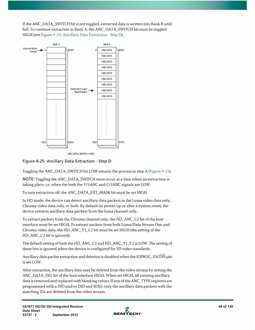
If the ANC_DATA_SWITCH bit is not toggled, extracted data is written into Bank B until full. To continue extraction in Bank A, the ANC_DATA_SWITCH bit must be toggled HIGH (see Figure 4-25: Ancillary Data Extraction - Step D).
Figure 4-25: Ancillary Data Extraction - Step D
Toggling the ANC_DATA_SWITCH bit LOW returns the process to step A (Figure 4-22).
NOTE: Toggling the ANC_DATA_SWITCH must occur at a time when no extraction is taking place, i.e. when the both the Y/1ANC and C/2ANC signals are LOW.
To turn extraction off, the ANC_DATA_EXT_MASK bit must be set HIGH.
In HD mode, the device can detect ancillary data packets in the Luma video data only, Chroma video data only, or both. By default (at power-up or after a system reset), the device extracts ancillary data packets from the luma channel only.
To extract packets from the Chroma channel only, the HD_ANC_C2 bit of the host interface must be set HIGH. To extract packets from both Luma/Data Stream One and Chroma video data, the HD_ANC_Y1_C2 bit must be set HIGH (the setting of the HD_ANC_C2 bit is ignored).
The default setting of both the HD_ANC_C2 and HD_ANC_Y1_C2 is LOW. The setting of these bits is ignored when the device is configured for SD video standards.
Ancillary data packet extraction and deletion is disabled when the IOPROC_EN/DIS pin is set LOW.
After extraction, the ancillary data may be deleted from the video stream by setting the ANC_DATA_DEL bit of the host interface HIGH. When set HIGH, all existing ancillary data is removed and replaced with blanking values. If any of the ANC_TYPE registers are programmed with a DID and/or DID and SDID, only the ancillary data packets with the matching IDs are deleted from the video stream.
0
1023
Application Layer Read Pointer
Internal Write Pointer
Bank A
ANC_DATA_SWITCH = HIGH
0
1023
Bank B
ANC DATA
ANC DATA
ANC DATA
ANC DATA
ANC DATA
ANC DATA
ANC DATA
ANC DATA
ANC DATA
800h 800h
BFFh800h
GS1671 HD/SD SDI Integrated ReceiverData Sheet53737 - 2 September 2012
64 of 130

NOTE 1: After the ancillary data determined by the ANC_TYPE_X_APX registers has been deleted, other existing ancillary data may not be contiguous. The device does not concatenate the remaining ancillary data.
NOTE 2: Reading extracted ancillary data from the host interface must be performed while there is a valid video signal present at the serial input and the device is locked (LOCKED signal is HIGH).
4.18 Audio De-embedderThe GS1671 includes an integrated audio de-embedder which is enabled by default in SMPTE mode. It can be disabled by setting the AUDIO_EN/DIS pin LOW, or by setting the host interface AUD_EXT_MASK bit to HIGH, or by keeping IOPROC_EN/DIS pin LOW. In non-SMPTE modes, the audio de-embedder is not active.
Up to eight channels of audio may be extracted from the received serial digital video stream. The output signal formats supported by the device include AES/EBU, I2S (default) and industry standard serial digital formats.
16, 20 and 24-bit audio bit depths are supported for 48kHz synchronous audio for SD data rates. For HD data rate, 16, 20 and 24-bit audio bit depths are supported for 48kHz audio. The audio may be synchronous or asynchronous to the video.
Additional audio processing features include audio mute on loss of lock, de-embed and delete, group selection, audio output re-mapping, ECC error detection and correction (HD mode only), and audio channel status extraction.
4.18.1 Serial Audio Data I/O Signals
The Serial Audio Data I/O pins are listed in Table 4-15: Serial Audio Pin Descriptions.
Table 4-15: Serial Audio Pin Descriptions
Audio
Pin Name Description
AUDIO_EN/DIS Enable Input for Audio Processing
AOUT_1/2 Serial Audio output; Channels 1 and 2
AOUT_3/4 Serial Audio output; Channels 3 and 4
AOUT_5/6 Serial Audio Output; Channels 5 and 6
AOUT_7/8 Serial Audio Output; Channels 7 and 8
ACLK 64fs clock
WCLK Word clock
AMCLK Audio Master Clock, selectable 128fs, 256fs, or 512fs
GS1671 HD/SD SDI Integrated ReceiverData Sheet53737 - 2 September 2012
65 of 130
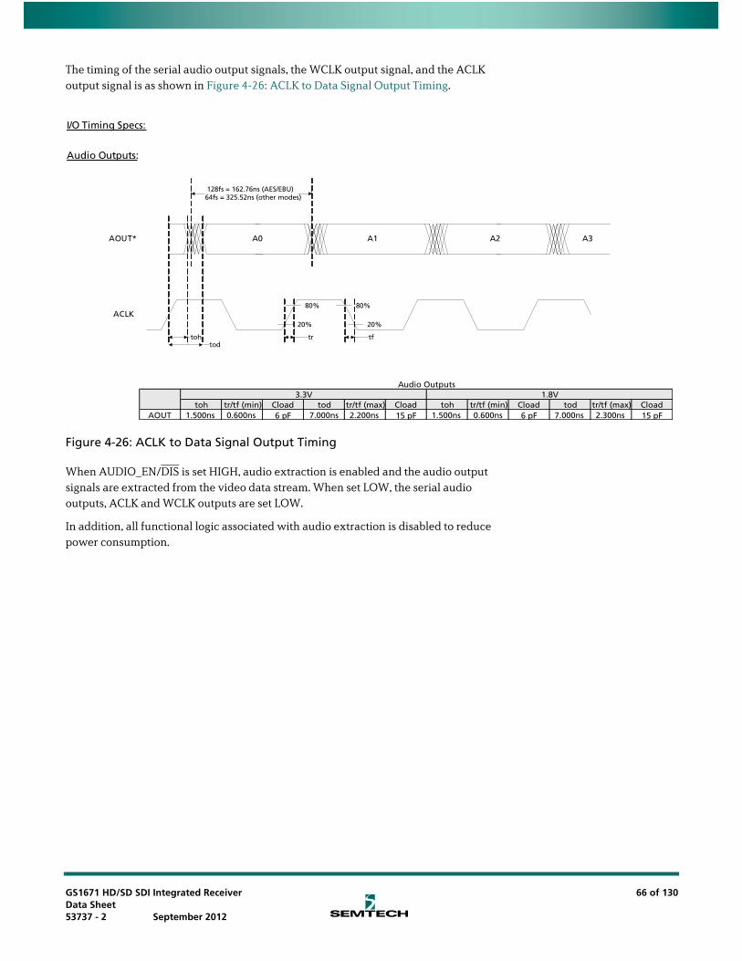
The timing of the serial audio output signals, the WCLK output signal, and the ACLK output signal is as shown in Figure 4-26: ACLK to Data Signal Output Timing.
Figure 4-26: ACLK to Data Signal Output Timing
When AUDIO_EN/DIS is set HIGH, audio extraction is enabled and the audio output signals are extracted from the video data stream. When set LOW, the serial audio outputs, ACLK and WCLK outputs are set LOW.
In addition, all functional logic associated with audio extraction is disabled to reduce power consumption.
I/O Timing Specs:
AOUT*
ACLK
A1A0 A2
128fs = 162.76ns (AES/EBU)64fs = 325.52ns (other modes)
20%
80%
tr
20%
80%
tf
A3
Audio Outputs:
tohtod
toh tr/tf (min) Cload tod tr/tf (max) Cload toh tr/tf (min) Cload tod tr/tf (max) CloadAOUT 1.500ns 0.600ns 6 pF 7.000ns 2.200ns 15 pF 1.500ns 0.600ns 6 pF 7.000ns 2.300ns 15 pF
Audio Outputs3.3V 1.8V
GS1671 HD/SD SDI Integrated ReceiverData Sheet53737 - 2 September 2012
66 of 130

4.18.2 Serial Audio Data Format Support
The GS1671 supports the following serial audio data formats:
• I2S (default)
• AES/EBU
• Serial Audio Left Justified, MSB First
• Serial Audio Left Justified, LSB First
• Serial Audio Right Justified, MSB First
• Serial Audio Right Justified, LSB First (this mode is not supported in SD)
By default (at power up or after system reset) I2S is selected. The other data formats are selectable via the host interface using the AMA/AMB[1:0] bits.
The serial audio output formats may use LSB first according to the settings of the control bits LSB_FIRSTA, LSB_FIRSTB, LSB_FIRSTC, and LSB_FIRSTD. When in I2S mode, these control bits must all be set LOW (default).
When I2S format is desired, both groups must be set to I2S (i.e. AMA = AMB = 11). This is because they share the same WCLK.
Figure 4-27: I2S Audio Output Format
Figure 4-28: AES/EBU Audio Output Format
Table 4-16: Audio Output Formats
AMA/AMB[1:0] Audio Output Format
00 AES/EBU audio output
01 Serial audio output: Left Justified; MSB first
10 Serial audio output: Right Justified; MSB first
11 I2S (Default)
WCLK
ACLK
AOUT[8/7:2/1]
MSB
032 12345622
LSB MSB
032 12345622
LSB
Channel A (Left)Channel B (Right)
WCLK
ACLK
AOUT[8/7:2/1] 1 2 3 4
LSB MSB
0
Channel A (Left) Channel B (Right)
5 6 7 8 27 2928 30 31 1 2 3 40 5 6 7 8 27 2928 30 31
AUXPreamble PCV U LSB MSBAUXPreamble PCV U
GS1671 HD/SD SDI Integrated ReceiverData Sheet53737 - 2 September 2012
67 of 130

Figure 4-29: Serial Audio, Left Justified, MSB First
Figure 4-30: Serial Audio, Left Justified, LSB First
Figure 4-31: Serial Audio, Right Justified, MSB First
Figure 4-32: Serial Audio, Right Justified, LSB First
4.18.2.1 AES/EBU Mode
In AES/EBU output mode, the audio de-embedder uses a 128fs (6.144MHz audio bit clock) clock as shown in Figure 4-33.
Figure 4-33: AES/EBU Audio Output to Bit Clock Timing
WCLK
ACLK
AOUT[8/7:2/1] 23
MSB
022 12345621
LSB
23
MSB
022 12345621
LSB
Channel A (Left) Channel B (Right)
WCLK
ACLK
AOUT[8/7:2/1] 0
LSB
321 2221201918172
MSB
0
LSB
321 2221201918172
MSB
Channel A (Left) Channel B (Right)
WCLK
ACLK
AOUT[8/7:2/1] 23
MSB
022 1220 17181921
LSB
23
MSB
022 1220 17181921
LSB
Channel A (Left) Channel B (Right)
WCLK
ACLK
AOUT[8/7:2/1] 0
LSB
321 22213 6542
MSB
0
LSB
321 22213 6542
MSB
Channel A (Left) Channel B (Right)
AMCLK (128fs)
AOUT_1/2, AOUT_3/4
AOUT_5/6, AOUT_7/8
6.144MHz
GS1671 HD/SD SDI Integrated ReceiverData Sheet53737 - 2 September 2012
68 of 130

4.18.2.2 Audio Data Packet Extraction Block
The audio de-embedder looks for audio data packets on every line of the incoming video.
The audio data must be embedded according to SMPTE 272M (SD) or SMPTE 299M (HD).
The Audio Group Detect registers are set HIGH when audio data packets with a corresponding group DID are detected in the input video stream. The host interface reports the individual audio groups detected.
When an audio data packet with a DID set in IDA[1:0] and IDB[1:0] is detected, the audio sample information is extracted and written into the audio FIFO.
The embedded audio group selected by IDA[1:0] is described henceforth in this document as Group A or Primary Group. The embedded audio group selected by IDB[1:0] is described henceforth in this document as Group B or Secondary Group.
Due to the large size of the horizontal ancillary data space in 720p/24, 720p/25 and 720p/30 video standards, the maximum number of ancillary data words the audio de-embedder can process is limited to 1024 when configured for these standards.
4.18.2.3 Audio Control Packets
The audio de-embedder automatically detects the presence of audio control packets in the video stream. When audio control packets for audio Group A are detected, the CTRA_DET bit of the host interface is set HIGH. When audio control packets for audio Group B are detected, the CTRB_DET bit of the host interface is set HIGH.
The audio control packet data is accessible via the host interface.
The audio control packets must be embedded according to SMPTE 272M (SD) or SMPTE 299M (HD).
NOTE: In SD, the control packet host interface registers are updated with new control packet values, after the CTRA_DET/CTRB_DET flags are cleared. In HD, the update happens automatically.
4.18.2.4 Setting Packet DID
Table 4-18 below, shows the 2-bit host interface setting for the audio group DID's.
For 24-bit audio support in SD mode, extended audio packets for Group A must have the same group DID set in IDA[1:0] of the host interface. Extended audio packets for Group B must have the same group DID set in IDB[1:0] of the host interface.
Table 4-17: Audio Data Packet Detect Register
Name Description Default
ADPG4_DET Audio Group Four Data Packet Detection (1: Detected) 0
ADPG3_DET Audio Group Three Data Packet Detection (1: Detected) 0
ADPG2_DET Audio Group Two Data Packet Detection (1: Detected) 0
ADPG1_DET Audio Group One Data Packet Detection (1: Detected) 0
GS1671 HD/SD SDI Integrated ReceiverData Sheet53737 - 2 September 2012
69 of 130

The audio de-embedder automatically detects the presence of extended audio packets. When detected, the audio output format is set to 24-bit audio sample word length.
The audio de-embedder defaults to audio Groups One and Two, where Group A is extracted from packets with audio Group One DID, and Group B from packets with audio Group Two DID.
4.18.2.5 Audio Packet Delete Block
To delete all ancillary data with a group DID shown in Table 4-18, the ALL_DEL bit in the host interface must be set HIGH.
4.18.2.6 ECC Error Detection & Correction Block (HD Mode Only)
The audio de-embedder performs BCH(31,25) forward error detection and correction, as described in SMPTE 299M. The error correction for all embedded audio data packets is activated when the host interface ECC_OFF bit is set LOW (default LOW). The audio de-embedder corrects any errors in both the audio output and the embedded packet.
When a one-bit error is detected in a bit array of the ECC protected region of the audio data packet with audio group DID set in IDA[1:0], the ECCA_ERROR flag is set HIGH. When a one-bit error is detected in the ECC protected region of the audio data packet with audio group DID set in IDB[1:0], the ECCB_ERROR flag is set HIGH.
Figure 4-34 shows examples of error correction and detection. Up to 8 bits in error can be corrected, providing each bit error is in a different bit array (shown below). When there are two or more bits in error in the same 24-bit array, the errors are detected, but not corrected.
Table 4-18: Audio Group DID Host Interface Settings
Audio Group
SD Data DID
SD Extended DID
HD Data DID
SD Control DID
HD Control DID
Host Interface Register Setting (2-bit)
1 2FFh 1FEh 2E7h 1EFh 1E3h 00b
2 1FDh 2FCh 1E6h 2EEh 2E2h 01b
3 1FBh 2FAh 1E5h 2EDh 2E1h 10b
4 2F9h 1F8h 2E4h 1ECh 1E0h 11b
Table 4-19: Audio Data and Control Packet DID Setting Register
Name Description Default
IDA[1-0] Group A Audio data and control packet DID setting 00b
IDB[1-0] Group B Audio data and control packet DID setting 01b
GS1671 HD/SD SDI Integrated ReceiverData Sheet53737 - 2 September 2012
70 of 130

Figure 4-34: ECC 24-bit Array and Examples
4.18.3 Audio Processing
4.18.3.1 Audio Clock Generation
For SD and HD audio, a single set of audio frequencies is generated for all audio channels, using a Direct Digital Period Synthesizer (DDPS) to minimize jitter.
In SD mode, audio clocks are derived from the PCLK.
In HD mode, the input control for the DDPS is derived from the two embedded audio clock phase words in the audio data packet corresponding to Group A. The audio clock phase information used is taken from the first embedded audio packet in the HANC space. With no embedded audio present, the device will not generate ACLK or WCLK. The IGNORE_PHASE bit should be asserted in this case to ensure the proper AMCLK frequency is generated.
The audio de-embedder also includes a Flywheel block to overcome any inconsistencies in the embedded audio clock phase information.
If the audio phase data is not present in the audio data packets, or is incorrect, the NO_PHASEA_DATA bit in the host interface is set and the clock will free-run based on the detected video format, the PCLK and the M value. IGNORE_PHASE should be set HIGH when NO_PHASEA_DATA is set. This does not occur automatically.
When the IGNORE_PHASE bit in the host interface is set HIGH, it is recommended that the M value be programmed via the host interface. This can be done by setting the FORCE_M bit HIGH, and programming the desired value into FORCE_MEQ1001. The correct value can be obtained by reading the M bit from the Video Core Registers.
If the DDPS is locked to phase data and audio data packets are lost or corrupted, the Clock Generator will flywheel for up to four audio data packets. If no valid audio data packet with valid phase data is provided within this time, the Clock Generator will free-run based on the video format, the PCLK and the M value.
Bit 7Bit 6Bit 5Bit 4Bit 3Bit 2Bit 1Bit 0
24-bit array
ADF ADF ADF DID DBN DC CLK CLK CH1 CH1 CH1 CH1 CH2 CH2 CH2 CH2 CH3 CH3 CH3 CH3 CH4 CH4 CH4 CH4Bit 7Bit 6Bit 5Bit 4Bit 3Bit 2Bit 1Bit 0
Errors corrected
ADF ADF ADF DID DBN DC CLK CLK CH1 CH1 CH1 CH1 CH2 CH2 CH2 CH2 CH3 CH3 CH3 CH3 CH4 CH4 CH4 CH4Bit 7Bit 6Bit 5Bit 4Bit 3Bit 2Bit 1Bit 0
Errors detected but not corrected
GS1671 HD/SD SDI Integrated ReceiverData Sheet53737 - 2 September 2012
71 of 130

If the IGNORE_PHASE bit in the host interface is HIGH, the clock will free-run based on the video format, the PCLK and the M value, independent of the NO_PHASEA_DATA bit.
In the 720p/24 video format, the total line length is 4125 pixels, which requires a resolution of 13 bits for the audio clock phase words in the embedded audio data packets. SMPTE 299M only specifies a maximum of 12 bits resolution. Proposed changes to SMPTE 299M suggest using bit 5 of UDW1 (currently reserved and set to zero) in the audio data packet as the MSB (ck13) for the audio clock phase data, providing 13 bits resolution.
Some audio encoders may hold the clock phase value at a maximum value when reached, until reset at the end of the line. This produces a small amount of audio phase jitter for the period of one sample.
To overcome this issue, the audio de-embedder checks for all cases. On detection of the maximum value, a comparison is made between previous clock phases and the correct position interpolated. If the clock phase data value starts to decrease, the de-embedder checks to see if bit 5 (ck13) of UDW1 in the audio data packet is set. If ck13 is set, the correct value is used. If ck13 is not set, the correct position is interpolated.
4.18.3.2 Detect 5-Frame Sequence Block
5-frame sequence detection is required for 525-line based video formats only. The audio de-embedder checks the Audio Frame Number sequence in the audio control packets, when present. If the audio frame sequence is running (repeated 1 to 5 count), the audio de-embedder uses this information to determine the 5-frame sequence. If the audio control packet is not present, or the Audio Frame Number words are set to 200h, the audio de-embedder detects the 5-frame sequence by counting the number of samples per frame. Figure 4-35 shows the number of samples per frame over a 5-frame sequence.
Figure 4-35: Sample Distribution over 5 Video Frames (525-line Systems)
When the audio inputs are asynchronously switched or disrupted, the audio de-embedder continues to write audio samples into the audio buffer, based on the current 5-frame sequence. The de-embedder then re-locks to the new 5-frame sequence, at which point a sample may be lost.
NOTE: In SD, all four channel pairs must follow the same 5-frame sequence.
Frame 1 1 emarF5 emarF4 emarF3 emarF2 emarF5 emarF
1602 2061206120612061 1601 1601
8008 Samples
1602 Repeat
GS1671 HD/SD SDI Integrated ReceiverData Sheet53737 - 2 September 2012
72 of 130

4.18.3.3 Audio FIFO Block
The function of the FIFO block is to change the audio data word rate from the ANC rate multiplexed with the video signal to the 48kHz audio output rate.
The audio FIFO block contains the audio sample buffers; one per audio channel. Each buffer is 36 audio samples deep. At power up or reset, the read pointer is held at the zero position until 26 samples have been written into the FIFO (allows for 6 lines per frame with no audio samples; a maximum of 4 samples per line in SD Mode). See Figure 4-36.
Figure 4-36: Audio Buffer After Initial 26 Sample Write
The position of the write pointer with respect to the read pointer is monitored continuously. If the write pointer is less than 6 samples ahead of the read pointer (point A in Figure 4-37), a sample is repeated from the read-side of the FIFO. If the write pointer is less than 6 samples behind the read pointer (point B in Figure 4-37), a sample is dropped. This avoids buffer underflow/overflow conditions.
Figure 4-37: Audio Buffer Pointer Boundary Checking
The repeat or drop sample operation is performed a maximum of 28 consecutive times, after which the audio outputs are muted (all sample data set to zero). In SD Mode, 26 samples are required to be written into the FIFO prior to starting the read operation again.
The audio buffer pointer offset may be reduced from 26 samples to 12 or 6 samples using the OS_SEL[1:0] bits in the host interface. The default setting is 26 samples (see Table 4-20).
Audio Buffer
0 25 35
Read Pointer
Write Pointer
Address
Audio Buffer
0 29 35
Read Pointer
Write Pointer
Write Pointer
A
5
B
Address
GS1671 HD/SD SDI Integrated ReceiverData Sheet53737 - 2 September 2012
73 of 130

When the OS_SEL[1:0] bits are set for 6-sample pointer offset, no boundary-checking is performed.
In HD mode the audio FIFO is a maximum of 10 samples deep. According to SMPTE 299M, audio samples are multiplexed immediately in the next HANC region after the audio sample occurs.
4.18.3.4 Audio Crosspoint Block
The Audio Crosspoint is used for audio output channel re-mapping. This feature allows any of the selected audio channels in Group A or Group B to be output on any of the eight output channels. The default setting is for one to one mapping, where AOUT_1/2 is extracted from Group A CH1 and CH2, AOUT_3/4 is extracted from Group A CH3 and CH4, and so on.
NOTE: If audio samples from embedded audio packets with the group set in IDA[1:0] are to be paired with samples from the group set in IDB[1:0], all of the channels must have been derived from the same Word Clock and must be synchronous.
The output channel is set in the OPn_SRC[2:0] host interface registers. Table 4-21 lists the 3-bit address for audio channel mapping.
Table 4-20: Audio Buffer Pointer Offset Settings
OS_SEL[1:0] Buffer Pointer Offset
00 26 samples (default)
01 12 samples
10 6 samples
Table 4-21: Audio Channel Mapping Codes
Audio Output Channel 3-bit Host InterfaceSource Address
1 000
2 001
3 010
4 011
5 100
6 101
7 110
8 111
GS1671 HD/SD SDI Integrated ReceiverData Sheet53737 - 2 September 2012
74 of 130

4.18.3.5 Serial Audio Output Word Length
The audio output, in serial modes, has a selectable 24, 20 or 16-bit sample word length. The ASWL[1:0] host interface register is used to configure the audio output sample word length. Figure 4-22 shows the host interface 2-bit code for setting the audio sample word length. When the presence of extended audio packets is detected in SD modes, the audio de-embedder defaults to 24-bit audio sample word length.
4.18.3.6 Audio Channel Status
The GS1671 detects the AES/EBU Audio Channel Status (ACS) block information for each of the selected channel pairs.
ACS data detection is indicated by corresponding ACS_DET flag bits in the host interface. The flag is cleared by writing to the same location.
Audio Channel Status Read
AES/EBU ACS data is available separately for each of the channels in a stereo pair. The GS1671 defaults to reading the first channel of each pair. There are 184 bits in each ACS packet, which are written to twelve 16-bit right-justified registers in the host interface.
The ACS_USE_SECOND bit (default LOW) selects the second channel in each audio pair when set HIGH.
Once all of the ACS data for a channel has been acquired, the corresponding ACS_DET bit is set, and acquisition stops. The ACS data is overwritten with new data when the ACS_DET bit is cleared in the system.
Audio Channel Status Regeneration
When the ACS_REGEN bit in the host interface is set HIGH, the audio de-embedder embeds the 24 bytes of the Audio Channel Status information programmed in the ACSR[183:0] registers into the 'C' bit of the AES/EBU outputs. The same Audio Channel Status information is used for all output channels.
In order to apply ACSR data;
• Set the ACS_REGEN bit to logic HIGH
• Write the desired ACSR data to the ACSR registers
Table 4-22: Audio Sample Word Lengths
ASWL[1:0] Audio Sample Word Length(SD)
Audio Sample Word Length(HD)
00 24-bit 24-bit
01 20-bit 20-bit
10 16-bit 16-bit
11 Auto 24/20-bit (Default) Reserved (Default)*
*NOTE: By default, for HD at power-up, the word length is invalid. The desired word length should be programmed through the host interface.
GS1671 HD/SD SDI Integrated ReceiverData Sheet53737 - 2 September 2012
75 of 130

• Set the ACS_APPLY bit to HIGH
At the next status boundary, the device outputs the contents of the ACSR registers as ACS data. This event may occur at a different time for each of the output channels. While waiting for the status boundary, the device sets the appropriate ACS_APPLY_WAIT[A:D] flag.
Table 4-23 shows the host interface default settings for the Audio Channel Status block. The audio de-embedder automatically generates the CRC word.
Table 4-23: Audio Channel Status Information Registers
Name Description Default
ACSR[7-0] Audio channel status block byte 0 set. Used when ACS_REGEN is set HIGH 85h
ACSR[15-8] Audio channel status block byte 1 set. Used when ACS_REGEN is set HIGH 08h
ACSR[23-16] Audio channel status block byte 2 set. Used when ACS_REGEN is set HIGH 28h (SD) 2Ch (HD)
ACSR[31-24]:
ACSR[183-176]
Audio channel status block data for bytes 3 to 22. Used when ACS_REGEN is set HIGH 00h
ACS_REGEN Audio channel status regenerate 0
ACS_APPLY Apply new ACSR data 0
ACS_APPLY_W
AIT[A:D]
Waiting to apply new ACSR data 0
ACS[7-0]:
ACS[183-176]
Audio channel status block data for bytes 0 to 22 00h: 00h
Table 4-24: Audio Channel Status Block for Regenerate Mode Default Settings
Name Byte Bit Default Mode
PRO 0 0 1b Professional use of channel status block
Emphasis 0 2-4 100b 100b None. Rec. manual override disabled
Sample Frequency 0 6-7 01b 48kHz. Manual override or auto disabled
Channel Mode 1 0-3 0001b Two channels. Manual override disabled
AUX 2 0-2 000b SD Modes: Maximum audio word length is 20 bits
001b HD Mode: Maximum audio word length is 24 bits
Source Word Length 2 3-5 101b Maximum word length (based on AUX setting).
24-bit for HD Mode; 20-bit for SD Modes
All other bits set to zero
GS1671 HD/SD SDI Integrated ReceiverData Sheet53737 - 2 September 2012
76 of 130

4.18.3.7 Audio Mute
When the MUTE bits in the host interface are set HIGH, the audio outputs are muted (all audio sample bits are set to zero). To set all the audio output channels to mute, set the host interface MUTE_ALL bit HIGH.
Mute On Loss Of Lock
When the GS1671 loses lock (LOCKED signal is LOW), the audio de-embedder sets all audio outputs LOW (no audio formatting is performed). The ACLK, WCLK and AMCLK outputs are also forced LOW.
4.18.4 Error Reporting
4.18.4.1 Data Block Number Error
When the 1-255 count sequence in the Data Block Number (DBN) word of Group A audio data packets is discontinuous, the DBNA_ERR bit in the host interface (DBN_ERR register for SD, ACS_DET register for HD) is set HIGH. When the 1-255 count sequence in the DBN word of Group B audio data packets is discontinuous, the DBNB_ERR bit in the host interface (DBN_ERR register for SD, ACS_DET register for HD) register is set HIGH.
4.18.4.2 ECC Error
The GS1671 monitors the ECC error status of the two selected audio groups, as described in Section 4.18.2.6 on page 70.
The ECC[N]_ERROR flags also have associated SD_AUDIO_ERROR_MASK and HD_AUDIO_ERROR_MASK register flags for configuration of error reporting in the Receiver. The ECC[N]_ERROR flags remain set until read via the host interface.
Table 4-25: Audio Mute Control Bits
Name Description Default
MUTE_ALL Ch1-8 audio mute enable (1: Enabled) 0
MUTE8 Ch8 audio mute enable (1: Enabled) 0
MUTE7 Ch7 audio mute enable (1: Enabled) 0
MUTE6 Ch6 audio mute enable (1: Enabled) 0
MUTE5 Ch5 audio mute enable (1: Enabled) 0
MUTE4 Ch4 audio mute enable (1: Enabled) 0
MUTE3 Ch3 audio mute enable (1: Enabled) 0
MUTE2 Ch2 audio mute enable (1: Enabled) 0
MUTE1 Ch1 audio mute enable (1: Enabled) 0
GS1671 HD/SD SDI Integrated ReceiverData Sheet53737 - 2 September 2012
77 of 130

4.19 GSPI - HOST InterfaceThe GSPI, or Gennum Serial Peripheral Interface, is a 4-wire interface provided to allow the system to access additional status and control information through configuration registers in the GS1671.
The GSPI is comprised of a Serial Data Input signal (SDIN), Serial Data Output signal (SDOUT), an active low Chip Select (CS), and a Burst Clock (SCLK).
Because these pins are shared with the JTAG interface port, an additional control signal pin JTAG/HOST is provided.
When JTAG/HOST is LOW, the GSPI interface is enabled. When JTAG/HOST is HIGH, the JTAG interface is enabled.
When operating in GSPI mode, the SCLK, SDIN, and CS signals must be provided by the system. The SDOUT pin is a non-clocked loop-through of SDIN and may be connected to the SDIN of another device, allowing multiple devices to be connected to the GSPI chain. See Section 4.19.2 for details. The interface is illustrated in the Figure 4-38 below.
Figure 4-38: GSPI Application Interface Connection
All read or write access to the GS1671 is initiated and terminated by the system host processor. Each access always begins with a Command/Address Word, followed by a data write to, or data read from, the GS1671.
4.19.1 Command Word Description
The Command Word consists of a 16-bit word transmitted MSB first and contains a read/write bit, an Auto-Increment bit and a 12-bit address.
Figure 4-39: Command Word Format
Command Words are clocked into the GS1671 on the rising edge of the Serial Clock SCLK, which operates in a burst fashion. The chip select (CS) signal must be set low a
Application Host
SCLK SCLK
SCLK
CS1
SDOUT SDIN
SDOUT
SDOUT
CS
SDIN
SDIN
CS2
GS1671
GS1671
CS
R/W RSV RSV AutoInc A0A1A2A3A4A5A6A7A8A9A11 A10
MSB LSB
GS1671 HD/SD SDI Integrated ReceiverData Sheet53737 - 2 September 2012
78 of 130

minimum of 1.5ns (t0 in Figure 4-41) before the first clock edge to ensure proper operation.
When the Auto-Increment bit is set LOW, each Command Word must be followed by only one Data Word to ensure proper operation.
If the Auto-Increment bit is set HIGH, the following Data Word is written into the address specified in the Command Word, and subsequent Data Words are written into incremental addresses from the first Data Word. This facilitates multiple address writes without sending a Command Word for each Data Word.
NOTE: The RSV bits in the GSPI command word can be set to zero as placeholder, though these bits are not used.
4.19.2 Data Read or Write Access
During a read sequence (Command Word R/W bit set HIGH) serial data is transmitted or received MSB first, synchronous with the rising edge of the serial clock SCLK. The Chip Select (CS) signal must be set low a minimum of 1.5ns (t0 in Figure 4-41) before the first clock edge to ensure proper operation. The first bit (MSB) of the Serial Output (SDOUT) is available (t5 in Figure 4-42) following the last falling SCLK edge of the read Command Word, the remaining bits are clocked out on the negative edges of SCLK.
NOTE: When several devices are connected to the GSPI chain, only one CS may be asserted during a read sequence.
During a write sequence (Command Word R/W bit set LOW), a wait state of 37.1ns (t4 in Figure 4-41) is required between the Command Word and the following Data Word. This wait state must also be maintained between successive Command Word/Data Word write sequences. When Auto Increment mode is selected (AutoInc = 1), the wait state must be maintained between successive Data Words after the initial Command Word/Data Word sequence.
During the write sequence, all Command and following Data Words input at the SDIN pin are output at the SDOUT pin unchanged. When several devices are connected to the GSPI chain, data can be written simultaneously to all the devices which have CS set LOW.
Figure 4-40: Data Word Format
D15 D14 D13 D12 D0D1D2D3D4D5D6D7D8D9D11 D10
MSB LSB
GS1671 HD/SD SDI Integrated ReceiverData Sheet53737 - 2 September 2012
79 of 130

4.19.3 GSPI Timing
Write and Read Mode timing for the GSPI interface;
Figure 4-41: Write Mode
Figure 4-42: Read Mode
Figure 4-43: GSPI Time Delay
R/W RSV RSVAuto_Inc A0A1A2A3A4A5A6A7A8A9A11 A10 D15 D14 D13 D12 D0D1D2D3D4D5D6D7D8D9D11 D10
SCLK _TCLK
CS _TMS
SDIN _TDI
SDOUT _TDO
t0
t3
t1
t2
R/W RSV RSV Auto_Inc A0A1A2A3A4A5A6A7A8A9A11 A10 D15 D14 D13 D12 D0D1D2D3D4D5D6D7D8D9D11 D10
t8
t4t7
R /W RSV RSVAuto_Inc A0A1A2A3A4A5A6A7A8A9A11 A10
D15 D14 D13 D12 D0D1D2D3D4D5D6D7D8D9D11 D10
SCLK _TCLK
CS _ TMS
SDIN_TDI
SDOUT _TDO
t5
R/W RSV RSV Auto_Inc A0A1A2A3A4A5A6A7A8A9A11 A10
t6
SDIN_TDI data_0
SDIN_TDI to SDOUT_TDO combinational path for daisy chain connection of multiple GS1671.
SDOUT_TDO data_0
TDELAY
Table 4-26: GSPI Time Delay
Parameter Symbol Conditions Min Typ Max Units
Delay time tDELAY 50% levels; 1.8V operation
− − 13.1 ns
Delay time tDELAY 50% levels; 3.3V operation
− − 9.7 ns
GS1671 HD/SD SDI Integrated ReceiverData Sheet53737 - 2 September 2012
80 of 130

This timing must be satisfied across all ambient temperature and power supply operating conditions, as described in the Electrical Characteristics on page 16.
Table 4-27: GSPI Timing Parameters (50% levels; 3.3V or 1.8V operation)
Parameter Symbol Min Typ Max Units
CS low before SCLK rising edge t0 1.5 − − ns
SCLK period t1 16.67 − − ns
SCLK duty cycle t2 40 50 60 %
Input data setup time t3 1.5 − − ns
Time between end of Command Word (or data in Auto-Increment mode) and the first SCLK of the following Data Word – write cycle
t4 PCLK (MHz) ns − − ns
unlocked 100
27.0 37.1
74.25 13.5
148.5 6.7
Time between end of Command Word (or data in Auto-Increment mode) and the first SCLK of the following Data Word – read cycle.
t5 PCLK (MHz) ns − − ns
unlocked −
27.0 148.4
74.25 53.9
148.5 27
Time between end of Command Word (or data in Auto-Increment mode) and the first SCLK of the following Data Word – read cycle - ANC FIFO Read
t5 222.6 − − ns
Output hold time (15pF load) t6 1.5 − − ns
CS high after last SCLK rising edge t7 PCLK (MHz) ns − − ns
unlocked 445
27.0 37.1
74.25 13.5
148.5 6.7
Input data hold time t8 1.5 − − ns
GS1671 HD/SD SDI Integrated ReceiverData Sheet53737 - 2 September 2012
81 of 130

4.20 Host Interface Register MapsNOTE: The GS1671 only accepts write/read commands to/from the Audio Register Maps when the audio core is locked to the incoming video data rate. The Video Register Map is always active, whether valid serial input data is present or not.
4.20.1 Video Core Registers
Table 4-28: Video Core Configuration and Status Registers
Address Register Name Bit Name Bit Description R/W Default
000h IOPROC_1 RSVD 15 Reserved. R 0
TRS_WORD_REMAP_DS1 _DISABLE
14 Disables 8-bit TRS word remapping for HD and SD inputs.
R/W 0
RSVD 13 Reserved. R/W 0
EDH_FLAG_UPDATE _MASK
12 Disables updating of EDH error flags.
R/W 0
EDH_CRC_INS_MASK 11 Disables EDH_CRC error correction and insertion.
R/W 0
H_CONFIG 10 Selects the H blanking indication:
0: Active line blanking - the H output is HIGH for all the horizontal blanking period, including the EAV and SAV TRS words.
1: TRS based blanking - the H output is set HIGH for the entire horizontal blanking period as indicated by the H bit in the received TRS signals.
This signal is only valid when TIM_861 is set to '0' (via pin or host interface).
R/W 0
ANC_DATA_EXT_MASK 9 Disables ancillary data extraction FIFO.
R/W 0
AUD_EXT_MASK 8 Disables audio extraction block. R/W 0
TIM_861_PIN_DISABLE 7 Disable TIM_861 pin control when set to '1', and use TIMING_861 bit instead.
R/W 0
TIMING_861 6 Selects the output timing reference format: 0 = Digital FVH timing output; 1 = CEA-861 timing output.
R/W 0
RSVD 5 Reserved. R/W 0
ILLEGAL_WORD_REMAP _DS1_MASK
4 Disables illegal word remapping for HD and SD inputs.
R/W 0
GS1671 HD/SD SDI Integrated ReceiverData Sheet53737 - 2 September 2012
82 of 130

000h IOPROC_1 ANC_CHECKSUM _INSERTION_DS1_MASK
3 Disables insertion of ancillary data checksums for HD and SD inputs.
R/W 0
CRC_INS_DS1_MASK 2 Disables insertion of HD CRC words for HD inputs.
R/W 0
LNUM_INS_DS1_MASK 1 Disables insertion of line numbers for HD inputs.
R/W 0
TRS_INS_DS1_MASK 0 Disables insertion of TRS words for HD and SD inputs.
R/W 0
001h IOPROC_2 RSVD 15-0 Reserved. R/W N/A
002h ERROR_STAT_1 RSVD 15-11 Reserved. ROCW 0
VD_STD_ERR_DS1 10 Video Standard Error indication for HD and SD inputs.
ROCW 0
FF_CRC_ERR 9 EDH Full Frame CRC error indication.
ROCW 0
AP_CRC_ERR 8 EDH Active Picture CRC error indication.
ROCW 0
RSVD 7 Reserved. ROCW 0
CCS_ERR_DS1 6 Chroma ancillary data checksum error indication for HD and SD inputs.
ROCW 0
YCS_ERR_DS1 5 Luma ancillary data checksum error indication for HD and SD inputs.
ROCW 0
CCRC_ERR_DS1 4 Chroma CRC error indication for HD inputs.
ROCW 0
YCRC_ERR_DS1 3 Luma CRC error indication for HD inputs.
ROCW 0
LNUM_ERR_DS1 2 Line number error indication for HD inputs.
ROCW 0
SAV_ERR_DS1 1 SAV error indication for HD and SD inputs.
ROCW 0
EAV_ERR_DS1 0 EAV error indication for HD and SD inputs.
ROCW 0
003h RSVD RSVD 15-0 Reserved. ROCW N/A
Table 4-28: Video Core Configuration and Status Registers (Continued)
Address Register Name Bit Name Bit Description R/W Default
GS1671 HD/SD SDI Integrated ReceiverData Sheet53737 - 2 September 2012
83 of 130

004h EDH_FLAG_IN EDH_DETECT 15 Embedded EDH packet detected. R 0
ANC_UES_IN 14 Ancillary data – unknown error status flag.
R 0
ANC_IDA_IN 13 Ancillary data – internal error detected already flag.
R 0
ANC_IDH_IN 12 Ancillary data – internal error detected here flag
R 0
ANC_EDA_IN 11 Ancillary data – error detected already flag.
R 0
ANC_EDH_IN 10 Ancillary data – error detected here flag.
R 0
FF_UES_IN 9 EDH Full Field – unknown error status flag.
R 0
FF_IDA_IN 8 EDH Full Field – internal error detected already flag.
R 0
FF_IDH_IN 7 EDH Full Field – internal error detected here flag.
R 0
FF_EDA_IN 6 EDH Full Field – error detected already flag.
R 0
FF_EDH_IN 5 EDH Full Field – error detected here flag.
R 0
AP_UES_IN 4 EDH Active Picture – unknown error status flag.
R 0
AP_IDA_IN 3 EDH Active Picture – internal error detected already flag.
R 0
AP_IDH_IN 2 EDH Active Picture – internal error detected here flag.
R 0
AP_EDA_IN 1 EDH Active Picture – error detected already flag.
R 0
AP_EDH_IN 0 EDH Active Picture – error detected here flag.
R 0
Table 4-28: Video Core Configuration and Status Registers (Continued)
Address Register Name Bit Name Bit Description R/W Default
GS1671 HD/SD SDI Integrated ReceiverData Sheet53737 - 2 September 2012
84 of 130

005h EDH_FLAG_OUT RSVD 15 Reserved. R 0
ANC_UES 14 Ancillary data – Unknown Error Status flag.
R 1
ANC_IDA 13 Ancillary data – Internal error Detected Already flag.
R 0
ANC_IDH 12 Ancillary data – Internal error Detected Here flag.
R 0
ANC_EDA 11 Ancillary data – Error Detected Already flag.
R 0
ANC_EDH 10 Ancillary data – Error Detected Here flag.
R 0
FF_UES 9 EDH Full Field – Unknown Error Status flag.
R 1
FF_IDA 8 EDH Full Field – Internal error Detected Already flag.
R 0
FF_IDH 7 EDH Full Field – Internal error Detected Here flag.
R 0
FF_EDA 6 EDH Full Field – Error Detected Already flag.
R 0
FF_EDH 5 EDH Full Field – Error Detected Here flag.
R 0
AP_UES 4 EDH Active Picture – Unknown Error Status flag.
R 1
AP_IDA 3 EDH Active Picture – Internal error Detected Already flag.
R 0
AP_IDH 2 EDH Active Picture – Internal error Detected Here flag.
R 0
AP_EDA 1 EDH Active Picture – Error Detected Already flag.
R 0
AP_EDH 0 EDH Active Picture – Error Detected Here flag.
R 0
006h DATA_FORMAT_DS1
FF_CRC_V 15 EDH Full Field CRC Validity bit. R 0
AP_CRC_V 14 EDH Active Picture CRC Validity bit. R 0
VD_STD_DS1 13-8 Detected Video Standard for HD and SD inputs.
R 29
CDATA_FORMAT_DS1 7-4 Data format as indicated in Chroma channel for HD and SD inputs.
R 15
YDATA_FORMAT_DS1 3-0 Data format as indicated in Luma channel for HD and SD inputs.
R 15
007h RSVD RSVD 15-0 Reserved. R N/A
Table 4-28: Video Core Configuration and Status Registers (Continued)
Address Register Name Bit Name Bit Description R/W Default
GS1671 HD/SD SDI Integrated ReceiverData Sheet53737 - 2 September 2012
85 of 130

008h IO_CONFIG RSVD 15 Reserved. RW 0
STAT2_CONFIG 14-10 Configure STAT2 output pin:
00000: H Blanking when TIM_861 = 0; HSYNC when TIM_861 = 1 00001: V Blanking when TIM_861 = 0; VSYNC when TIM_861 = 1 00010: F bit when TIM_861 = 0; Data Enable (DE) when TIM_861 = 1 00011: LOCKED 00100: Y/1ANC: ANC indication (SD), Luma ANC indication (HD) 00101: C/2ANC: Chroma ANC indication (HD) 00110: Data Error 00111: Video Error 01000: Audio Error 01001: EDH Detected 01010: Carrier Detect 01011: RATE_DET 01100 - 11111: Reserved
RW 2
STAT1_CONFIG 9-5 Configure STAT1 output pin. (Refer to above for decoding)
RW 1
STAT0_CONFIG 4-0 Configure STAT0 output pin. (Refer to above for decoding)
RW 0
009h IO_CONFIG2 RSVD 15 Reserved. RW 0
STAT5_CONFIG 14-10 Configure STAT5 output pin. (Refer to above for decoding)
RW 6
STAT4_CONFIG 9-5 Configure STAT4 output pin. (Refer to above for decoding)
RW 4
STAT3_CONFIG 4-0 Configure STAT3 output pin. (Refer to above for decoding)
RW 3
00Ah ANC_CONTROL RSVD 15-4 Reserved. RW 0
ANC_DATA_SWITCH 3 Switches between FIFO memories. RW 0
ANC_DATA_DEL 2 Remove Ancillary Data from output video stream, set to Luma and Chroma blanking values.
RW 0
HD_ANC_Y1_C2 1 Extract Ancillary data from Luma and Chroma channels (HD inputs).
RW 0
HD_ANC_C2 0 Extract Ancillary data only from Chroma channel (HD inputs).
RW 0
00Bh ANC_LINE_A RSVD 15-11 Reserved. R/W 0
ANC_LINE_A 10-0 Video Line to extract Ancillary data from.
R/W 0
00Ch ANC_LINE_B RSVD 15-11 Reserved. R/W 0
ANC_LINE_B 10-0 Second video Line to extract Ancillary data from.
R/W 0
Table 4-28: Video Core Configuration and Status Registers (Continued)
Address Register Name Bit Name Bit Description R/W Default
GS1671 HD/SD SDI Integrated ReceiverData Sheet53737 - 2 September 2012
86 of 130

00Dh - 00Eh
RSVD RSVD 15-0 Reserved. R 0
00Fh ANC_TYPE_1_AP1
ANC_TYPE1_DS1 15-0 Programmable DID/SDID pair #1 to extract from HD and SD input formats ([15:8] = DID, [7:0] =SDID).
R/W 0
010h ANC_TYPE_2_AP1
ANC_TYPE2_DS1 15-0 Programmable DID/SDID pair #2 to extract from HD and SD input formats ([15:8] = DID, [7:0] =SDID).
R/W 0
011h ANC_TYPE_3_AP1
ANC_TYPE3_DS1 15-0 Programmable DID/SDID pair #3 to extract from HD and SD input formats ([15:8] = DID, [7:0] =SDID).
R/W 0
012h ANC_TYPE_4_AP1
ANC_TYPE4_DS1 15-0 Programmable DID/SDID pair #4 to extract from HD and SD input formats ([15:8] = DID, [7:0] =SDID).
R/W 0
013h ANC_TYPE_5
_AP1
ANC_TYPE5_DS1 15-0 Programmable DID/SDID pair #5 to extract from HD and SD input formats ([15:8] = DID, [7:0] =SDID).
R/W 0
014h - 018h
RSVD RSVD 15-0 Reserved. R/W N/A
019h VIDEO_FORMAT_352_A_1
VIDEO_FORMAT_2_DS1 15-8 SMPTE 352M embedded packet – byte 2.
R 0
VIDEO_FORMAT_1_DS1 7-0 SMPTE 352M embedded packet – byte 1: [7]: Version identifier [6:0]: Video Payload Identifier.
R 0
01Ah VIDEO_FORMAT_352_B_1
VIDEO_FORMAT_4_DS1 15-8 SMPTE 352M embedded packet – byte 4.
R 0
VIDEO_FORMAT_3_DS1 7-0 SMPTE 352M embedded packet – byte 3.
R 0
01Bh - 01Eh
RSVD RSVD 15-0 Reserved. R/W N/A
01Fh RASTER_STRUC_1
RSVD 15-14 Reserved. R 0
WORDS_PER_ACTLINE 13-0 Words Per Active Line. R 0
020h RASTER_STRUC_2
RSVD 15-14 Reserved. R 0
WORDS_PER_LINE 13-0 Total Words Per Line. R 0
021h RASTER_STRUC_3
RSVD 15-11 Reserved. R 0
LINES_PER_FRAME 10-0 Total Lines Per Frame. R 0
Table 4-28: Video Core Configuration and Status Registers (Continued)
Address Register Name Bit Name Bit Description R/W Default
GS1671 HD/SD SDI Integrated ReceiverData Sheet53737 - 2 September 2012
87 of 130

022h RASTER_STRUC_4
RATE_SEL_READBACK 15-14 Read back detected data rate:
0 = HD, 1,3=SD, 2=Reserved
R 0
M 13 Specifies detected M value
0: 1.000 1: 1.001
R 0
Note: In certain systems, due to greater ppm offset in the crystal, the ‘M’ bit may not assert properly. In such cases, bits 3:0 in Register 06Fh can be increased to a maximum value of 4.
STD_LOCK 12 Video standard lock. R 0
INT_PROG 11 Interlaced or progressive. R 0
ACTLINE_PER_FIELD 10-0 Active lines per frame. R 0
023h FLYWHEEL_STATUS
RSVD 15-2 Reserved. R 0
V_LOCK_DS1 1 Indicates that the timing signal generator is locked to vertical timing (HD and SD inputs).
R 0
H_LOCK_DS1 0 Indicates that the timing signal generator is locked to horizontal timing (HD and SD inputs).
R 0
024h RATE_SEL RSVD 15-3 Reserved. R 0
AUTO/MAN 2 Detect data rate automatically (1) or program manually (0).
R/W 1
RATE_SEL_TOP 1-0 Programmable rate select in manual mode:
0 = HD, 1,3=SD, 2=Reserved
R/W 0
025h TIM_861_FORMAT
RSVD 15-7 Reserved. R 0
FORMAT_ERR 6 Indicates standard is not recognized for CEA 861 conversion.
R 1
FORMAT_ID_861 5-0 CEA-861 format ID of input video stream. Refer to Table 4-9.
R 0
026h TIM_861_CFG RSVD 15-3 Reserved. R 0
VSYNC_INVERT 2 Invert output VSYNC pulse. R/W 0
HSYNC_INVERT 1 Invert output HSYNC pulse. R/W 0
TRS_861 0 Sets the timing reference outputs to DFP timing mode when set to '1'. By default, the timing reference outputs follow CEA-861 timing mode. Only valid when TIM_861 is set to '1'.
R/W 0
027h - 036h
RSVD RSVD − Reserved. R 0
Table 4-28: Video Core Configuration and Status Registers (Continued)
Address Register Name Bit Name Bit Description R/W Default
GS1671 HD/SD SDI Integrated ReceiverData Sheet53737 - 2 September 2012
88 of 130

037h ERROR_MASK_1 RSVD 15-11 Reserved. R 0
ERROR_MASK_1 10-0 Error mask for global error vector (HD, SD):
bit[0]: EAV_ERR_DS1 mask bit[1]: SAV_ERR_DS1 mask bit[2]: LNUM_ERR_DS1 mask bit[3]: YCRC_ERR_DS1 mask bit[4]: CCRC_ERR_DS1 mask bit[5]: YCS_ERR_DS1 mask bit[6]: CCS_ERR_DS1 mask bit[7]: Reserved bit[8]: AP_CRC_ERR mask bit[9]: FF_CRC_ERR mask bit[10]: VD_STD_ERR_DS1 mask
R/W 0
038h ERROR_MASK_2 RSVD 15-0 Reserved. R 0
039h ACGEN_CTRL RSVD 15-5 Reserved. R 0
SCLK_INV 4 Invert polarity of output serial audio clock.
R/W 0
AMCLK_INV 3 Invert polarity of output audio master clock.
R/W 0
RSVD 2 Reserved. R/W 0
AMCLK_SEL 1-0 Audio Master Clock Select.
0: 128 fs 1: 256 fs 2: 512 fs
R/W 0
03Ah-6Bh
RSVD RSVD 15-0 Reserved. R 0
06Ch CLK_GEN RSVD 15-5 Reserved. R/W 0
DEL_LINE_OFFSET 4-0 Controls the offset for the delay line.
R/W 0
Table 4-28: Video Core Configuration and Status Registers (Continued)
Address Register Name Bit Name Bit Description R/W Default
GS1671 HD/SD SDI Integrated ReceiverData Sheet53737 - 2 September 2012
89 of 130

06Dh IO_DRIVE_STRENGTH
RSVD 15-6 Reserved. R/W 0
IO_DS_CTRL_DOUT_MSB 5-4 Drive strength adjustment for DOUT[19:10] outputs and PCLK output:
00: 4mA; 01: 8mA; 10: 10mA(1.8V), 12mA(3.3V); 11: 12mA(1.8V), 16mA(3.3V)
R/W 2
IO_DS_CTRL_STAT 3-2 Drive strength adjustment for STAT[5:0] outputs:
00: 4mA; 01: 6mA; 10: 8mA(1.8V), 10mA(3.3V); 11: 10mA(1.8V), 12mA(3.3V)
R/W 2
IO_DS_CTRL_DOUT_LSB 1-0 Drive strength adjustment for DOUT[9:0] outputs:
00: 4mA; 01: 6mA; 10: 8mA(1.8V), 10mA(3.3V); 11: 10mA(1.8V), 12mA(3.3V)
R/W 3
06Eh- 072h
RSVD RSVD − Reserved. R/W 0
073h EQ_BYPASS RSVD 15-10 Reserved. R/W 0
EQ_BYPASS 9 0: non-bypass EQ 1: bypass EQ
R/W 0
RSVD 8-0 Reserved. R/W 0
074h-085h
RSVD RSVD 15-0 Reserved. R/W 0
Table 4-28: Video Core Configuration and Status Registers (Continued)
Address Register Name Bit Name Bit Description R/W Default
GS1671 HD/SD SDI Integrated ReceiverData Sheet53737 - 2 September 2012
90 of 130

4.20.2 SD Audio Core Registers
NOTE: The GS1671 only accepts write/read commands to/from the SD Audio Register Map when the audio core is locked to the incoming SD video format.
Table 4-29: SD Audio Core Configuration and Status Registers
Address Register Name Bit Name Bit Description R/W Default
400h CFG_AUD RSVD 15-14 Reserved. R/W 0
ALL_DEL 13 Selects deletion of all audio data and all audio control packets. 0: Do not delete existing audio packets 1: Delete existing audio packets
R/W 0
MUTE_ALL 12 Mute all output channels. 0: Normal 1: Muted
R/W 0
ACS_USE_SECOND 11 Extract Audio Channel Status from second channel pair.
R/W 0
CLEAR_AUDIO 10 Clears all audio FIFO buffers and puts them in start-up state.
R/W 0
OS_SEL 9-8 Specifies the audio FIFO buffer size. 00: 36 samples deep, 26 sample start-up count 01: 22 samples deep, 12 sample start-up count 10: 16 samples deep, 6 sample start-up count 11: Reserved
R/W 0
LSB_FIRSTD 7 Causes the channel 7 and 8 output format to use LSB first. 0: MSB first 1: LSB first
R/W 0
LSB_FIRSTC 6 Causes the channel 5 and 6 output format to use LSB first. 0: MSB first 1: LSB first
R/W 0
LSB_FIRSTB 5 Causes the channel 3 and 4 output format to use LSB first. 0: MSB first 1: LSB first
R/W 0
LSB_FIRSTA 4 Causes the channel 1 and 2 output format to use LSB first. 0: MSB first 1: LSB first
R/W 0
GS1671 HD/SD SDI Integrated ReceiverData Sheet53737 - 2 September 2012
91 of 130

400h CFG_AUD IDB 3-2 Specifies the Secondary audio group to extract. 00: Audio group #1 01: Audio group #2 10: Audio group #3 11: Audio group #4 Note: Should IDA and IDB be set to the same value, they automatically revert to their default values.
R/W 1
IDA 1-0 Specifies the Primary audio group to extract.
00: Audio group #1 01: Audio group #2 10: Audio group #3 11: Audio group #4 Note: Should IDA and IDB be set to the same value, they automatically revert to their default values.
R/W 0
401h DBN_ERR EXT_DET3_4B 15 Set when Secondary group channels 3 and 4 have extended data. Write ‘1’ to clear.
ROCW 0
EXT_DET1_2B 14 Set when Secondary group channels 1 and 2 have extended data. Write ‘1’ to clear.
ROCW 0
EXT_DET3_4A 13 Set when Primary group channels 3 and 4 have extended data. Write ‘1’ to clear.
ROCW 0
EXT_DET1_2A 12 Set when Primary group channels 1 and 2 have extended data. Write ‘1’ to clear.
ROCW 0
CTL_DBNB_ERR 11 Set when Secondary group control packet Data Block Number sequence is discontinuous. Write ‘1’ to clear.
ROCW 0
CTL_DBNA_ERR 10 Set when Primary group control packet Data Block Number sequence is discontinuous. Write ‘1’ to clear.
ROCW 0
EXT_DBNB_ERR 9 Set when Secondary group extended data packet Data Block Number sequence is discontinuous. Write ‘1’ to clear.
ROCW 0
EXT_DBNA_ERR 8 Set when Primary group extended data packet Data Block Number sequence is discontinuous. Write ‘1’ to clear.
ROCW 0
Table 4-29: SD Audio Core Configuration and Status Registers (Continued)
Address Register Name Bit Name Bit Description R/W Default
GS1671 HD/SD SDI Integrated ReceiverData Sheet53737 - 2 September 2012
92 of 130

401h DBN_ERR SAMP_DBNB_ERR 7 Set when Secondary group data packet Data Block Number sequence is discontinuous. Write ‘1’ to clear.
ROCW 0
SAMP_DBNA_ERR 6 Set when Primary group data packet Data Block Number sequence is discontinuous. Write ‘1’ to clear.
ROCW 0
CTRB_DET 5 Set when Secondary group audio control packet is detected. Write ‘1’ to clear.
ROCW 0
CTRA_DET 4 Set when Primary group audio control packet is detected. Write ‘1’ to clear.
ROCW 0
ACS_DET3_4B 3 Secondary group audio status detected for channels 3 and 4. Write ‘1’ to clear.
ROCW 0
ACS_DET1_2B 2 Secondary group audio status detected for channels 1 and 2. Write ‘1’ to clear.
ROCW 0
ACS_DET3_4A 1 Primary group audio status detected for channels 3 and 4. Write ‘1’ to clear.
ROCW 0
ACS_DET1_2A 0 Primary group audio status detected for channels 1 and 2. Write ‘1’ to clear.
ROCW 0
402h REGEN RSVD 15-2 Reserved. R/W 0
ACS_APPLY 1 Cause channel status data in ACSR[183:0] to be transferred to the channel status replacement mechanism. The transfer does not occur until the next status boundary.
R/W 0
ACS_REGEN 0 Specifies that Audio Channel Status of all channels should be replaced with ACSR[183:0] field. 0: Do not replace Channel Status 1: Replace Channel Status of all channels
R/W 0
Table 4-29: SD Audio Core Configuration and Status Registers (Continued)
Address Register Name Bit Name Bit Description R/W Default
GS1671 HD/SD SDI Integrated ReceiverData Sheet53737 - 2 September 2012
93 of 130

403h AUD_DET IDB_READBACK 15-14 Actual value of IDB in the hardware.
R 1
IDA_READBACK 13-12 Actual value of IDA in the hardware.
R 0
XDPG4_DET 11 Set while embedded Group 4 audio extended packets are detected.
R 0
XDPG3_DET 10 Set while embedded Group 3 audio extended packets are detected.
R 0
XDPG2_DET 9 Set while embedded Group 2 audio extended packets are detected.
R 0
XDPG1_DET 8 Set while embedded Group 1 audio extended packets are detected.
R 0
ADPG4_DET 7 Set while Group 4 audio data packets are detected.
R 0
ADPG3_DET 6 Set while Group 3 audio data packets are detected.
R 0
ADPG2_DET 5 Set while Group 2 audio data packets are detected.
R 0
ADPG1_DET 4 Set while Group 1 audio data packets are detected.
R 0
ACS_APPLY_WAITD 3 Set while output channels 7 and 8 are waiting for a status boundary to apply the ACSR[183:0] data.
R 0
ACS_APPLY_WAITC 2 Set while output channels 5 and 6 are waiting for a status boundary to apply the ACSR[183:0] data.
R 0
ACS_APPLY_WAITB 1 Set while output channels 3 and 4 are waiting for a status boundary to apply the ACSR[183:0] data.
R 0
ACS_APPLY_WAITA 0 Set while output channels 1 and 2 are waiting for a status boundary to apply the ACSR[183:0] data.
R 0
404h CSUM_ERR_DET RSVD 15-1 Reserved. R/W 0
CSUM_ERROR 0 Embedded packet checksum error detected. Write ‘1’ to clear.
ROCW 0
405h CH_MUTE RSVD 15-8 Reserved. R/W 0
MUTE 7-0 Mute output channels 8..1 Where bits 7:0 = channel 8:1 1: Mute 0: Normal
R/W 0
Table 4-29: SD Audio Core Configuration and Status Registers (Continued)
Address Register Name Bit Name Bit Description R/W Default
GS1671 HD/SD SDI Integrated ReceiverData Sheet53737 - 2 September 2012
94 of 130

406h CH_VALID RSVD 15-8 Reserved. R/W 0
CH4_VALIDB 7 Secondary group channel 4 sample validity flag.
R 0
CH3_VALIDB 6 Secondary group channel 3 sample validity flag.
R 0
CH2_VALIDB 5 Secondary group channel 2 sample validity flag.
R 0
CH1_VALIDB 4 Secondary group channel 1 sample validity flag.
R 0
CH4_VALIDA 3 Primary group channel 4 sample validity flag.
R 0
CH3_VALIDA 2 Primary group channel 3 sample validity flag.
R 0
CH2_VALIDA 1 Primary group channel 2 sample validity flag.
R 0
CH1_VALIDA 0 Primary group channel 1 sample validity flag.
R 0
407h SD_AUDIO_ERROR_MASK
RSVD 15 Reserved. R/W 0
EN_NOT_LOCKED 14 Asserts interrupt when LOCKED signal is not asserted.
R/W 0
EN_NO_VIDEO 13 Asserts interrupt when video format is unknown.
R/W 0
EN_CSUM_ERROR 12 Asserts interrupt when checksum error is detected.
R/W 0
EN_ACS_DET3_4B 11 Asserts interrupt when EN_ACS_DET3_4B flag is set.
R/W 0
EN_ACS_DET1_2B 10 Asserts interrupt when EN_ACS_DET1_2B flag is set.
R/W 0
EN_ACS_DET3_4A 9 Asserts interrupt when EN_ACS_DET3_4A flag is set.
R/W 0
EN_ACS_DET1_2A 8 Asserts interrupt when EN_ACS_DET1_2A flag is set.
R/W 0
EN_CTRB_DET 7 Asserts interrupt when EN_CTRB_DET flag is set.
R/W 0
EN_CTRA_DET 6 Asserts interrupt when EN_CTRA_DET flag is set.
R/W 0
EN_DBNB_ERR 5 Asserts interrupt when EN_DBNB_ERR flag is set.
R/W 0
EN_DBNA_ERR 4 Asserts interrupt when EN_DBNA_ERR flag is set.
R/W 0
Table 4-29: SD Audio Core Configuration and Status Registers (Continued)
Address Register Name Bit Name Bit Description R/W Default
GS1671 HD/SD SDI Integrated ReceiverData Sheet53737 - 2 September 2012
95 of 130

407h SD_AUDIO_ERROR_MASK
EN_ADPG4_DET 3 Asserts interrupt when the ADPG4_DET flag is set.
R/W 0
EN_ADPG3_DET 2 Asserts interrupt when the ADPG3_DET flag is set.
R/W 0
EN_ADPG2_DET 1 Asserts interrupt when the ADPG2_DET flag is set.
R/W 0
EN_ADPG1_DET 0 Asserts interrupt when the ADPG1_DET flag is set.
R/W 0
408h CFG_OUTPUT ASWLD 15-14 Output channels 7 and 8 word length. 00: 24 bits 01: 20 bits 10: 16 bits 11: Automatic 20-bit or 24-bit
R/W 3
ASWLC 13-12 Output channels 5 and 6 word length. (See above for decoding)
R/W 3
ASWLB 11-10 Output channels 3 and 4 word length. (See above for decoding)
R/W 3
ASWLA 9-8 Output channels 1 and 2 word length. (See above for decoding)
R/W 3
AMD 7-6 Output channels 7 and 8 format selector. 00: AES/EBU audio output 01: Serial audio output: Left justified; MSB first 10: Serial audio output: Right justified; MSB first 11: I2S serial audio output
R/W 3
AMC 5-4 Output channels 5 and 6 format selector. (See above for decoding).
R/W 3
AMB 3-2 Output channels 3 and 4 format selector. (See above for decoding).
R/W 3
AMA 1-0 Output channels 1 and 2 format selector. (See above for decoding).
R/W 3
Table 4-29: SD Audio Core Configuration and Status Registers (Continued)
Address Register Name Bit Name Bit Description R/W Default
GS1671 HD/SD SDI Integrated ReceiverData Sheet53737 - 2 September 2012
96 of 130

409h OUTPUT_SEL_1 RSVD 15-12 Reserved. R/W 0
OP4_SRC 11-9 Output channel 4 source selector. 000: Primary audio group channel 1 001: Primary audio group channel 2 010: Primary audio group channel 3 011: Primary audio group channel 4 100: Secondary audio group channel 1 101: Secondary audio group channel 2 110: Secondary audio group channel 3 111: Secondary audio group channel 4
R/W 3
OP3_SRC 8-6 Output channel 3 source selector (Decode as above).
R/W 2
OP2_SRC 5-3 Output channel 2 source selector (Decode as above).
R/W 1
OP1_SRC 2-0 Output channel 1 source selector (Decode as above).
R/W 0
40Ah OUTPUT_SEL_2 RSVD 15-12 Reserved. R/W 0
OP8_SRC 11-9 Output channel 8 source selector. 000: Primary audio group channel 1 001: Primary audio group channel 2 010: Primary audio group channel 3 011: Primary audio group channel 4 100: Secondary audio group channel 1 101: Secondary audio group channel 2 110: Secondary audio group channel 3 111: Secondary audio group channel 4
R/W 7
OP7_SRC 8-6 Output channel 7 source selector (Decode as above).
R/W 6
OP6_SRC 5-3 Output channel 6 source selector (Decode as above).
R/W 5
OP5_SRC 2-0 Output channel 5 source selector (Decode as above).
R/W 4
40Bh - 41Fh
RSVD RSVD − Reserved. − −
Table 4-29: SD Audio Core Configuration and Status Registers (Continued)
Address Register Name Bit Name Bit Description R/W Default
GS1671 HD/SD SDI Integrated ReceiverData Sheet53737 - 2 September 2012
97 of 130

420h AFNA12 RSVD 15-9 Reserved. R/W 0
AFN1_2A 8-0 Primary group audio frame number for channels 1 and 2.
R 0
421h AFNA34 RSVD 15-9 Reserved. R/W 0
AFN3_4A 8-0 Primary group audio frame number for channels 3 and 4.
R 0
422h RATEA RSVD 15-8 Reserved. R/W 0
RATE3_4A 7-5 Primary group sampling frequency for channels 3 and 4
R 0
ASX3_4A 4 Primary group asynchronous mode for channels 3 and 4.
R 0
RATE1_2A 3-1 Primary group sampling frequency for channels 1 and 2.
R 0
ASX1_2A 0 Primary group asynchronous mode for channels 1 and 2.
R 0
423h ACT_A RSVD 15-4 Reserved. R/W 0
ACTA 3-0 Primary group active channels. R 0
424h PRIM_AUD_DELAY_1
RSVD 15-9 Reserved. R/W 0
DEL1A_1 8-1 Primary Audio group delay data for channel 1.
R 0
EBIT1A 0 Primary Audio group delay data valid flag for channel 1.
R 0
425h PRIM_AUD_DELAY_2
RSVD 15-9 Reserved. R/W 0
DEL1A_2 8-0 Primary Audio group delay data for channel 1.
R 0
426h PRIM_AUD_DELAY_3
RSVD 15-9 Reserved. R/W 0
DEL1A_3 8-0 Primary Audio group delay data for channel 1.
R 0
427h PRIM_AUD_DELAY_4
RSVD 15-9 Reserved. R/W 0
DEL2A_4 8-1 Primary Audio group delay data for channel 2.
R 0
EBIT2A 0 Primary Audio group delay data valid flag for channel 2.
R 0
428h PRIM_AUD_DELAY_5
RSVD 15-9 Reserved. R/W 0
DEL2A_5 8-0 Primary Audio group delay data for channel 2.
R 0
429h PRIM_AUD_DELAY_6
RSVD 15-9 Reserved. R/W 0
DEL2A_6 8-0 Primary Audio group delay data for channel 2.
R 0
Table 4-29: SD Audio Core Configuration and Status Registers (Continued)
Address Register Name Bit Name Bit Description R/W Default
GS1671 HD/SD SDI Integrated ReceiverData Sheet53737 - 2 September 2012
98 of 130

42Ah PRIM_AUD_DELAY_7
RSVD 15-9 Reserved. R/W 0
DEL3A_7 8-1 Primary Audio group delay data for channel 3.
R 0
EBIT3A 0 Primary Audio group delay data valid flag for channel 3.
R 0
42Bh PRIM_AUD_DELAY_8
RSVD 15-9 Reserved. R/W 0
DEL3A_8 8-0 Primary Audio group delay data for channel 3.
R 0
42Ch PRIM_AUD_DELAY_9
RSVD 15-9 Reserved. R/W 0
DEL3A_9 8-0 Primary Audio group delay data for channel 3.
R 0
42Dh PRIM_AUD_DELAY_10
RSVD 15-9 Reserved. R/W 0
DEL4A_10 8-1 Primary Audio group delay data for channel 4.
R 0
EBIT4A 0 Primary Audio group delay data valid flag for channel 4.
R 0
42Eh PRIM_AUD_DELAY_11
RSVD 15-9 Reserved. R/W 0
DEL4A_11 8-0 Primary Audio group delay data for channel 4.
R 0
42Fh PRIM_AUD_DELAY_12
RSVD 15-9 Reserved. R/W 0
DEL4A_12 8-0 Primary Audio group delay data for channel 4.
R 0
430h AFNB12 RSVD 15-9 Reserved. R/W 0
AFN1_2B 8-0 Secondary group audio frame number for channels 1 and 2.
R 0
431h AFNB34 RSVD 15-9 Reserved. R/W 0
AFN3_4B 8-0 Secondary group audio frame number for channels 3 and 4.
R 0
432h RATEB RSVD 15-8 Reserved. R 0
RATE3_4B 7-5 Secondary group sampling frequency for channels 3 and 4.
R 0
ASX3_4B 4 Secondary group asynchronous mode for channels 3 and 4.
R 0
RATE1_2B 3-1 Secondary group sampling frequency for channels 1 and 2.
R 0
ASX1_2B 0 Secondary group asynchronous mode for channels 1 and 2.
R 0
433h ACT_B RSVD 15-4 Reserved. R/W 0
ACTB 3-0 Secondary group active channels. R 0
Table 4-29: SD Audio Core Configuration and Status Registers (Continued)
Address Register Name Bit Name Bit Description R/W Default
GS1671 HD/SD SDI Integrated ReceiverData Sheet53737 - 2 September 2012
99 of 130

434h SEC_AUD_DELAY_!
RSVD 15-9 Reserved. R/W 0
DEL1B_1 8-1 Secondary Audio group delay data for channel 1.
R 0
EBIT1B 0 Secondary Audio group delay data valid flag for channel 1.
R 0
435h SEC_AUDDELAY_2
RSVD 15-9 Reserved. R/W
DEL1B_2 8-0 Secondary Audio group delay data for channel 1.
R 0
436h SEC_AUD_DELAY_3
RSVD 15-9 Reserved. R/W 0
DEL1B_3 8-0 Secondary Audio group delay data for channel 1.
R 0
437h SEC_AUDDELAY_4
RSVD 15-9 Reserved. R/W 0
DEL2B_4 8-1 Secondary Audio group delay data for channel 2.
R 0
EBIT2B 0 Secondary Audio group delay data valid flag for channel 2.
R 0
438h SEC_AUDDELAY_5
RSVD 15-9 Reserved. R/W 0
DEL2B_5 8-0 Secondary Audio group delay data for channel 2.
R 0
439h SEC_AUDDELAY_6
RSVD 15-9 Reserved. R/W 0
DEL2B_6 8-0 Secondary Audio group delay data for channel 2.
R 0
43Ah SEC_AUDDELAY_7
RSVD 15-9 Reserved. R/W 0
DEL3B_7 8-1 Secondary Audio group delay data for channel 3.
R 0
EBIT3B 0 Secondary Audio group delay data valid flag for channel 3.
R 0
43Bh SEC_AUDDELAY_8
RSVD 15-9 Reserved. R/W 0
DEL3B_8 8-0 Secondary Audio group delay data for channel 3.
R 0
43Ch SEC_AUDDELAY_9
RSVD 15-9 Reserved. R/W 0
DEL3B_9 8-0 Secondary Audio group delay data for channel 3.
R 0
43Dh SEC_AUDDELAY_10
RSVD 15-9 Reserved. R/W 0
DEL4B_10 8-1 Secondary Audio group delay data for channel 4.
R 0
EBIT4B 0 Secondary Audio group delay data valid flag for channel 4.
R 0
Table 4-29: SD Audio Core Configuration and Status Registers (Continued)
Address Register Name Bit Name Bit Description R/W Default
GS1671 HD/SD SDI Integrated ReceiverData Sheet53737 - 2 September 2012
100 of 130

43Eh SEC_AUD_DELAY_11
RSVD 15-9 Reserved. R/W 0
DEL4B_11 8-0 Secondary Audio group delay data for channel 4.
R 0
43Fh SEC_AUD_DELAY_12
RSVD 15-9 Reserved. R/W 0
DEL4B_12 8-0 Secondary Audio group delay data for channel 4.
R 0
440h ACSR1_2A_BYTE0_1
ACSR1_2A_0 15-0 Bytes 0 [7:0] and 1 [15:8] of audio group A channel status for channels 1 and 2
R 0
441h ACSR1_2A_BYTE2_3
ACSR1_2A_2 15-0 Bytes 2 [7:0] and 3 [15:8] of audio group A channel status for channels 1 and 2
R 0
442h ACSR1_2A_BYTE4_5
ACSR1_2A_4 15-0 Bytes 4 [7:0] and 5 [15:8] of audio group A channel status for channels 1 and 2
R 0
443h ACSR1_2A_BYTE6_7
ACSR1_2A_6 15-0 Bytes 6 [7:0] and 7 [15:8]of audio group A channel status for channels 1 and 2
R 0
444h ACSR1_2A_BYTE8_9
ACSR1_2A_8 15-0 Bytes 8 [7:0] and 9 [15:8] of audio group A channel status for channels 1 and 2.
R 0
445H ACSR1_2A_BYTE10_11
ACSR1_2A_10 15-0 Bytes 10 [7:0] and 11 [15:8] of audio group A channel status for channels 1 and 2.
R 0
446H ACSR1_2A_BYTE12_13
ACSR1_2A_12 15-0 Bytes 12 [7:0] and 13 [15:8] of audio group A channel status for channels 1 and 2.
R 0
447h ACSR1_2A_BYTE14_15
ACSR1_2A_14 15-0 Bytes 14 [7:0] and 15 [15:8] of audio group A channel status for channels 1 and 2.
R 0
448h ACSR1_2A_BYTE16_17
ACSR1_2A_16 15-0 Bytes 16 [7:0] and 17 [15:8] of audio group A channel status for channels 1 and 2.
R 0
449h ACSR1_2A_BYTE18_19
ACSR1_2A_18 15-0 Bytes 18 [7:0] and 19 [15:8] of audio group A channel status for channels 1 and 2.
R 0
44Ah ACSR1_2A_BYTE20_21
ACSR1_2A_20 15-0 Bytes 20 [7:0] and 21 [15:8] of audio group A channel status for channels 1 and 2.
R 0
44Bh ACRS1_2A_BYTE22
RSVD 15-8 Reserved. R/W 0
ACSR1_2A_22 7-0 Bytes 22 of audio group A channel status for channels 1 and 2.
R 0
44Ch - 44Fh
RSVD RSVD 15-0 Reserved. R/W 0
Table 4-29: SD Audio Core Configuration and Status Registers (Continued)
Address Register Name Bit Name Bit Description R/W Default
GS1671 HD/SD SDI Integrated ReceiverData Sheet53737 - 2 September 2012
101 of 130

450h ACSR3_4ABYTE0_1
ACSR3_4A_0 15-0 Bytes 0 [7:0] and 1 [15:8] of audio group A channel status for channels 3 and 4.
R 0
451h ACSR3_4ABYTE2_3
ACSR3_4A_2 15-0 Bytes 2 [7:0] and 3 [15:8] of audio group A channel status for channels 3 and 4.
R 0
452h ACSR3_4A_BYTE4_5
ACSR3_4A_4 15-0 Bytes 4 [7:0] and 5 [15:8] of audio group A channel status for channels 3 and 4.
R 0
453h ACSR3_4A_BYTE6_7
ACSR3_4A_6 15-0 Bytes 6 [7:0] and 7 [15:8] of audio group A channel status for channels 3 and 4.
R 0
454h ACSR3_4A_BYTE8_9
ACSR3_4A_8 15-0 Bytes 8 [7:0] and 9 [15:8] of audio group A channel status for channels 3 and 4.
R 0
455h ACSR3_4A_BYTE10_11
ACSR3_4A_10 15-0 Bytes 10 [7:0] and 11 [15:8] of audio group A channel status for channels 3 and 4.
R 0
456h ACSR3_4A_BYTE12_13
ACSR3_4A_12 15-0 Bytes 12 [7:0] and 13 [15:8] of audio group A channel status for channels 3 and 4.
R 0
457h ACSR3_4A_BYTE14_15
ACSR3_4A_14 15-0 Bytes 14 [7:0] and 15 [15:8] of audio group A channel status for channels 3 and 4.
R 0
458h ACSR3_4A_BYTE16_17
ACSR3_4A_16 15-0 Bytes 16 [7:0] and 17 [15:8] of audio group A channel status for channels 3 and 4.
R 0
459h ACSR3_4A_BYTE18_19
ACSR3_4A_18 15-0 Bytes 18 [7:0] and 19 [15:8] of audio group A channel status for channels 3 and 4.
R 0
45Ah ACSR3_4A_BYTE20_21
ACSR3_4A_20 15-0 Bytes 20 [7:0] and 21 [15:8] of audio group A channel status for channels 3 and 4.
R 0
45Bh ACSR3_4A_BYTE22
RSVD 15-8 Reserved. R/W 0
ACSR3_4A_22 7-0 Bytes 22 of audio group A channel status for channels 3 and 4.
R 0
45Ch - 45Fh
RSVD RSVD 15-0 Reserved. R/W 0
460h ACSR1_2B_BYTE0_1
ACSR1_2B_0 15-0 Bytes 0 [7:0] and 1 [15:8] of audio group B channel status for channels 1 and 2.
R 0
461h ACSR1_2B_BYTE2_3
ACSR1_2B_2 15-0 Bytes 2 [7:0] and 3 [15:8] of audio group B channel status for channels 1 and 2.
R 0
462h ACSR1_2B_BYTE4_5
ACSR1_2B_4 15-0 Bytes 4 [7:0] and 5 [15:8] of audio group B channel status for channels 1 and 2.
R 0
Table 4-29: SD Audio Core Configuration and Status Registers (Continued)
Address Register Name Bit Name Bit Description R/W Default
GS1671 HD/SD SDI Integrated ReceiverData Sheet53737 - 2 September 2012
102 of 130

463h ACSR1_2B_BYTE6_7
ACSR1_2B_6 15-0 Bytes 6 [7:0] and 7 [15:8] of audio group B channel status for channels 1 and 2.
R 0
464h ACSR1_2B_BYTE8_9
ACSR1_2B_8 15-0 Bytes 8 [7:0] and 9 [15:8] of audio group B channel status for channels 1 and 2.
R 0
465h ACSR1_2B_BYTE10_11
ACSR1_2B_10 15-0 Bytes 10 [7:0] and 11 [15:8] of audio group B channel status for channels 1 and 2.
R 0
466h ACSR1_2B_BYTE12_13
ACSR1_2B_12 15-0 Bytes 12 [7:0] and 13 [15:8] of audio group B channel status for channels 1 and 2.
R 0
467h ACSR1_2B_BYTE14_15
ACSR1_2B_14 15-0 Bytes 14 [7:0] and 15 [15:8] of audio group B channel status for channels 1 and 2.
R 0
468h ACSR1_2B_BYTE16_17
ACSR1_2B_16 15-0 Bytes 16 [7:0] and 17 [15:8] of audio group B channel status for channels 1 and 2.
R 0
469h ACSR1_2B_BYTE18_19
ACSR1_2B_18 15-0 Bytes 18 [7:0] and 19 [15:8] of audio group B channel status for channels 1 and 2.
R 0
46Ah ACSR1_2B_BYTE20_21
ACSR1_2B_20 15-0 Bytes 20 [7:0] and 21 [15:8] of audio group B channel status for channels 1 and 2.
R 0
46Bh ACSR1_2B_BYTE22
RSVD 15-8 Reserved. R/W 0
ACSR1_2B_22 7-0 Bytes 22 of audio group B channel status for channels 1 and 2.
R 0
46Ch - 46Fh
RSVD RSVD 15-0 Reserved. R/W 0
470h ACSR3_4B_BYTE0_1
ACSR3_4B_0 15-0 Bytes 0 [7:0] and 1 [15:8] of audio group B channel status for channels 3 and 4.
R 0
471h ACSR3_4B_BYTE2_3
ACSR3_4B_2 15-0 Bytes 2 [7:0] and 3 [15:8] of audio group B channel status for channels 3 and 4.
R 0
472h ACSR3_4B_BYTE4_5
ACSR3_4B_4 15-0 Bytes 4 [7:0] and 5 [15:8] of audio group B channel status for channels 3 and 4.
R 0
473h ACSR3_4B_BYTE6_7
ACSR3_4B_6 15-0 Bytes 6 [7:0] and 7 [15:8] of audio group B channel status for channels 3 and 4.
R 0
474h ACSR3_4B_BYTE8_9
ACSR3_4B_8 15-0 Bytes 8 [7:0] and 9 [15:8] of audio group B channel status for channels 3 and 4.
R 0
475h ACSR3_4B_BYTE10_11
ACSR3_4B_10 15-0 Bytes 10 [7:0] and 11 [15:8] of audio group B channel status for channels 3 and 4.
R 0
Table 4-29: SD Audio Core Configuration and Status Registers (Continued)
Address Register Name Bit Name Bit Description R/W Default
GS1671 HD/SD SDI Integrated ReceiverData Sheet53737 - 2 September 2012
103 of 130

476h ACSR3_4B_BYTE12_13
ACSR3_4B_12 15-0 Bytes 12 [7:0] and 13 [15:8] of audio group B channel status for channels 3 and 4.
R 0
477h ACSR3_4B_BYTE14_15
ACSR3_4B_14 15-0 Bytes 14 [7:0] and 15 [15:8] of audio group B channel status for channels 3 and 4.
R 0
478h ACSR3_4A_BYTE16_17
ACSR3_4B_16 15-0 Bytes 16 [7:0] and 17 [15:8] of audio group B channel status for channels 3 and 4.
R 0
479h ACSR3_4A_BYTE18_19
ACSR3_4B_18 15-0 Bytes 18 [7:0] and 19 [15:8] of audio group B channel status for channels 3 and 4.
R 0
47Ah ACSR3_4A_BYTE20_21
ACSR3_4B_20 15-0 Bytes 20 [7:0] and 21 [15:8] of audio group B channel status for channels 3 and 4.
R 0
47Bh ACSR3_4A_BYTE22
RSVD 15-8 Reserved. R/W 0
ACSR3_4B_22 7-0 Bytes 22 of audio group B channel status for channels 3 and 4.
R 0
47Ch - 47Fh
RSVD RSVD 15-0 Reserved. R/W 0
480h ACSR_BYTE_0 ACSR_BYTE0 7-0 Audio channel status to use when ACS_REGEN is set or when adding audio channel status to non-AES/EBU audio. 8 bits per register for 23 registers.
R 0
481h ACSR_BYTE_1 ACSR_BYTE1 7-0 − W 0
482h ACSR_BYTE_2 ACSR_BYTE2 7-0 − W 0
483h ACSR_BYTE_3 ACSR_BYTE3 7-0 − W 0
484h ACSR_BYTE_4 ACSR_BYTE4 7-0 − W 0
485h ACSR_BYTE_5 ACSR_BYTE5 7-0 − W 0
486h ACSR_BYTE_6 ACSR_BYTE6 7-0 − W 0
487h ACSR_BYTE_7 ACSR_BYTE7 7-0 − W 0
488h ACSR_BYTE_8 ACSR_BYTE8 7-0 − W 0
489h ACSR_BYTE_9 ACSR_BYTE9 7-0 − W 0
48Ah ACSR_BYTE_10 ACSR_BYTE10 7-0 − W 0
48Bh ACSR_BYTE_11 ACSR_BYTE11 7-0 − W 0
48Ch ACSR_BYTE_12 ACSR_BYTE12 7-0 − W 0
48Dh ACSR_BYTE_13 ACSR_BYTE13 7-0 − W 0
48Eh ACSR_BYTE_14 ACSR_BYTE14 7-0 − W 0
48Fh ACSR_BYTE_15 ACSR_BYTE15 7-0 − W 0
490h ACSR_BYTE_16 ACSR_BYTE16 7-0 − W 0
Table 4-29: SD Audio Core Configuration and Status Registers (Continued)
Address Register Name Bit Name Bit Description R/W Default
GS1671 HD/SD SDI Integrated ReceiverData Sheet53737 - 2 September 2012
104 of 130

491h ACSR_BYTE_17 ACSR_BYTE17 7-0 − W 0
492h ACSR_BYTE_18 ACSR_BYTE18 7-0 − W 0
493h ACSR_BYTE_19 ACSR_BYTE19 7-0 − W 0
494h ACSR_BYTE_20 ACSR_BYTE20 7-0 − R/W 0
495h ACSR_BYTE_21 ACSR_BYTE21 7-0 − R/W 0
496h ACSR_BYTE_22 ACSR_BYTE22 7-0 − R/W 0
Table 4-29: SD Audio Core Configuration and Status Registers (Continued)
Address Register Name Bit Name Bit Description R/W Default
GS1671 HD/SD SDI Integrated ReceiverData Sheet53737 - 2 September 2012
105 of 130

4.20.3 HD Audio Core Registers
NOTE: The GS1671 only accepts write/read commands to/from the HD Audio Register Map when the audio core is locked to the incoming HD video format.
Table 4-30: HD Audio Core Configuration and Status Registers
Address Register Name Bit Name Bit Description R/W Default
200h CFG_AUD ECC_OFF 15 Disables ECC error correction. R/W 0
ALL_DEL 14 Selects deletion of all audio data and all audio control packets
0: Do not delete existing audio control packets 1: Delete existing audio control packets.
R/W 0
MUTE_ALL 13 Mute all output channels
0: Normal 1: Muted
R/W 0
ACS_USE_SECOND 12 Extract Audio Channel Status from second channel pair.
R/W 0
ASWLB 11-10 Secondary group output word length.
00: 24 bits 01: 20 bits 10: 16 bits 11: invalid
R/W 3
ASWLA 9-8 Primary group output word length.
00: 24 bits 01: 20 bits 10: 16 bits 11: invalid
R/W 3
AMB 7-6 Secondary group output format selector.
00: AES/EBU audio output 01: Serial audio output: left justified MSB first 10: Serial audio output: right justified. MSB first 11: I2S serial audio output
R/W 3
AMA 5-4 Primary group output format selector.
00: AES/EBU audio output 01: Serial audio output: left justified MSB first 10: Serial audio output: right justified MSB first 11: I2S serial audio output
R/W 3
GS1671 HD/SD SDI Integrated ReceiverData Sheet53737 - 2 September 2012
106 of 130

200h CFG_AUD IDB 3-2 Specifies the Secondary audio group to extract.
00: Audio group #1 01: Audio group #2 10: Audio group #3 11: Audio group #4 Note: Should IDA and IDB be set to the same value, they automatically revert to their default values.
R/W 1
IDA 1-0 Specifies the Primary audio group to extract.
00: Audio group #1 01: Audio group #2 10: Audio group #3 11: Audio group #4 Note: Should IDA and IDB be set to the same value, they automatically revert to their default values.
R/W 0
201h ACS_DET RSVD 15-8 Reserved. R/W 0
DBNB_ERR 7 Set when Secondary group audio Data Block Number sequence is discontinuous.
ROCW 0
DBNA_ERR 6 Set when Primary group audio Data Block Number sequence is discontinuous.
ROCW 0
CTRB_DET 5 Set when Secondary group audio control packet is detected.
ROCW 0
CTRA_DET 4 Set when Primary group audio control packet is detected.
ROCW 0
ACS_DET3_4B 3 Secondary group audio status detected for channels 3 and 4.
ROCW 0
ACS_DET1_2B 2 Secondary group audio status detected for channels 1 and 2.
ROCW 0
ACS_DET3_4A 1 Primary group audio status detected for channels 3 and 4.
ROCW 0
ACS_DET1_2A 0 Primary group audio status detected for channels 1 and 2.
ROCW 0
Table 4-30: HD Audio Core Configuration and Status Registers (Continued)
Address Register Name Bit Name Bit Description R/W Default
GS1671 HD/SD SDI Integrated ReceiverData Sheet53737 - 2 September 2012
107 of 130

202h AUD_DET1 RSVD 15-9 Reserved. R 0
IDB_READBACK 8-7 Actual value of IDB in the hardware.
R 1
IDA_READBACK 6-5 Actual value of IDA in the hardware.
R 0
ADPG4_DET 4 Set while Group 4 audio data packets are detected.
R 0
ADPG3_DET 3 Set while Group 3 audio data packets are detected.
R 0
ADPG2_DET 2 Set while Group 2 audio data packets are detected.
R 0
ADPG1_DET 1 Set while Group 1 audio data packets are detected.
R 0
ACS_APPLY_WAIT 0 ACS_APPLY_WAIT: Set while output channels 1 and 2 are waiting for a status boundary to apply the ACSR[183:0] data.
R 0
203h AUD_DET2 RSVD 15-2 Reserved. R/W 0
ECCA_ERROR 1 Primary group audio data packet error detected.
ROCW 0
ECCB_ERROR 0 Secondary group audio data packet error detected.
ROCW 0
204h REGEN RSVD 15-2 Reserved. R/W 0
ACS_APPLY 1 Cause channel status data in ACSR[183:0] to be transferred to the channel status replacement mechanism. The transfer does not occur until the next status boundary.
R/W 0
ACS_REGEN 0 Specifies that Audio Channel Status of all channels should be replaced with ACSR[183:0] field.
0: Do not replace Channel Status 1: Replace Channel Status of all channels
R/W 0
205h CH_MUTE RSVD 15 Reserved. R/W 0
MUTEB 7-4 Mute Secondary output channels 4..1 Where bits 7:4 = channel 4:1
1: Mute 0: Normal
R/W 0
MUTEA 3-0 Mute Primary output channels 4..1 Where bits 3:0 = channel 4:1
1: Mute 0: Normal
R/W 0
Table 4-30: HD Audio Core Configuration and Status Registers (Continued)
Address Register Name Bit Name Bit Description R/W Default
GS1671 HD/SD SDI Integrated ReceiverData Sheet53737 - 2 September 2012
108 of 130

206h CH_VALID RSVD 15-8 Reserved. R/W 0
CH4_VALIDB 7 Secondary group channel 4 sample validity flag.
R 0
CH3_VALIDB 6 Secondary group channel 3 sample validity flag.
R 0
CH2_VALIDB 5 Secondary group channel 2 sample validity flag.
R 0
CH1_VALIDB 4 Secondary group channel 1 sample validity flag.
R 0
CH4_VALIDA 3 Primary group channel 4 sample validity flag.
R 0
CH3_VALIDA 2 Primary group channel 3 sample validity flag.
R 0
CH2_VALIDA 1 Primary group channel 2 sample validity flag.
R 0
CH1_VALIDA 0 Primary group channel 1 sample validity flag.
R 0
Table 4-30: HD Audio Core Configuration and Status Registers (Continued)
Address Register Name Bit Name Bit Description R/W Default
GS1671 HD/SD SDI Integrated ReceiverData Sheet53737 - 2 September 2012
109 of 130

207h HD_AUDIO_ERROR_MASK
RSVD 15 Reserved. R/W 0
EN_MISSING_PHASE 14 Asserts AUDIO_ERROR when chosen group's phase data is missing
R/W 0
EN_ACS_DET3_4B 13 Asserts AUDIO_ERROR when ACS_DET3_4B flag is set.
R/W 0
EN_ACS_DET1_2B 12 Asserts AUDIO_ERROR when ACS_DET1_2B flag is set.
R/W 0
EN_ACS_DET3_4A 11 Asserts AUDIO_ERROR when ACS_DET3_4A flag is set.
R/W 0
EN_ACS_DET1_2A 10 Asserts AUDIO_ERROR when ACS_DET1_2A flag is set.
R/W 0
EN_CTRB_DET 9 Asserts AUDIO_ERROR when CTRB_DET flag is set.
R/W 0
EN_CTRA_DET 8 Asserts AUDIO_ERROR when CTRA_DET flag is set.
R/W 0
EN_DBNB_ERR 7 Asserts AUDIO_ERROR when DBNB_ERR flag is set.
R/W 0
EN_DBNA_ERR 6 Asserts AUDIO_ERROR when DBNA_ERR flag is set.
R/W 0
EN_ECCB_ERR 5 Asserts AUDIO_ERROR when ECCB_ERR flag is set.
R/W 0
EN_ECCA_ERR 4 Asserts AUDIO_ERROR when ECCA_ERR flag is set.
R/W 0
EN_ADPG4_DET 3 Asserts AUDIO_ERROR when ADPG4_DET flag is set.
R/W 0
EN_ADPG3_DET 2 Asserts AUDIO_ERROR when ADPG3_DET flag is set.
R/W 0
EN_ADPG2_DET 1 Asserts AUDIO_ERROR when ADPG2_DET flag is set.
R/W 0
EN_ADPG1_DET 0 Asserts AUDIO_ERROR when ADPG1_DET flag is set.
R/W 0
Table 4-30: HD Audio Core Configuration and Status Registers (Continued)
Address Register Name Bit Name Bit Description R/W Default
GS1671 HD/SD SDI Integrated ReceiverData Sheet53737 - 2 September 2012
110 of 130

208h CFG_AUD_2 RSVD 15-11 Reserved. R/W 0
SEL_PHASE_SRC 10 Selects between the Primary and Secondary embedded phase info.
R/W 0
LSB_FIRSTB 9 Causes the Secondary group serial output formats to use LSB first.
R/W 0
LSB_FIRSTA 8 Causes the Primary group serial output formats to use LSB first.
R/W 0
FORCE_M 7 Disables M value detection and forces M value to that specified by FORCE_MEQ1001.
R/W 0
FORCE_MEQ1001 6 Specifies M value when FORCE_M is set.
1: M= 1.001 0: M = 1.000
R/W 0
IGNORE_PHASE 5 Causes the Demultiplexer to ignore the embedded clock info in both the Primary and Secondary group audio data packets. Clock is generated based on the video format and M value.
R/W 0
FORCE_ACLK128 4 Causes the core to ignore embedded clock info and derive phase information from ACLK128.
R/W 0
EN_NOT_LOCKED 3 Asserts AUDIO_ERROR when locked is not asserted.
R/W 0
EN_NO_VIDEO 2 Asserts AUDIO_ERROR when the video format is unknown.
R/W 0
EN_NO_PHASEB 1 Asserts AUDIO_ERROR when NO_PHASEB_DATA is set.
R/W 0
EN_NO_PHASEA 0 Asserts AUDIO_ERROR when NO_PHASEA_DATA is set.
R/W 0
209h CFG_AUD_3 RSVD 15-3 Reserved. R/W 0
MISSING_PHASE 2 Embedded phase info for chosen group missing or incorrect.
R 0
NO_PHASEB_DATA 1 Secondary group has invalid embedded clock information.
R 0
NO_PHASEA_DATA 0 Primary group has invalid embedded clock information.
R 0
Table 4-30: HD Audio Core Configuration and Status Registers (Continued)
Address Register Name Bit Name Bit Description R/W Default
GS1671 HD/SD SDI Integrated ReceiverData Sheet53737 - 2 September 2012
111 of 130

20Ah OUTPUT_SEL_1 RSVD 15-12 Reserved. R 0
OP4_SRC 11-9 Output channel 4 source selector.
000: Primary audio group channel 1 001: Primary audio group channel 2 010: Primary audio group channel 3 011: Primary audio group channel 4 100: Secondary audio group channel 1 101: Secondary audio group channel 2 110: Secondary audio group channel 3 111: Secondary audio group channel 4
R/W 3
OP3_SRC 8-6 Output channel 3 source selector (Decode as above).
R/W 2
OP2_SRC 5-3 Output channel 2 source selector (Decode as above).
R/W 1
OP1_SRC 2-0 Output channel 1 source selector (Decode as above).
R/W 0
20Bh OUTPUT_SEL_2 RSVD 15-12 Reserved. R/W 0
OP8_SRC 11-9 Output channel 8 source selector.
000: Primary audio group channel 1 001: Primary audio group channel 2 010: Primary audio group channel 3 011: Primary audio group channel 4 100: Secondary audio group channel 1 101: Secondary audio group channel 2 110: Secondary audio group channel 3 111: Secondary audio group channel 4
R/W 7
OP7_SRC 8-6 Output channel 7 source selector (Decode as above).
R/W 6
OP6_SRC 5-3 Output channel 6 source selector (Decode as above).
R/W 5
OP5_SRC 2-0 Output channel 5 source selector (Decode as above).
R/W 4
20Ch - 21Fh
RSVD RSVD − Reserved. − −
220h AFNA RSVD 15-9 Reserved. R/W 0
AFNA 8-0 Primary group audio frame number.
R 0
Table 4-30: HD Audio Core Configuration and Status Registers (Continued)
Address Register Name Bit Name Bit Description R/W Default
GS1671 HD/SD SDI Integrated ReceiverData Sheet53737 - 2 September 2012
112 of 130

221h RATEA RSVD 15-4 Reserved. R/W 0
RATEA 3-1 Primary group sampling frequency for channels 1 and 2.
R 0
ASXA 0 Primary group asynchronous mode for channels 1 and 2.
R 0
222h ACTA RSVD 15-4 Reserved. R/W 0
ACTA 3-0 Primary group active channels. R 0
223h PRIM_AUD_DELAY_1
RSVD 15-9 Reserved. R/W 0
DEL1_2A_1 8-1 Primary Audio group delay data for channels 1 and 2 [7:0].
R 0
EBIT1_2A 0 Primary Audio group delay data valid flag for channels 1 and 2.
R 0
224h PRIM_AUD_DELAY_2
RSVD 15-9 Reserved. R/W 0
DEL1_2A_2 8-0 Primary Audio group delay data for channels 1 and 2 [16:8].
R 0
225h PRIM_AUD_DELAY_3
RSVD 15-9 Reserved. R/W 0
DEL1_2A_3 8-0 Primary Audio group delay data for channels 1 and 2 [25:17].
R 0
226h PRIM_AUD_DELAY_4
RSVD 15-9 Reserved. R/W 0
DEL3_4A_4 8-1 Primary Audio group delay data for channels 3 and 4 [7:0].
R 0
EBIT3_4A 0 Primary Audio group delay data valid flag for channels 3 and 4.
R 0
227h PRIM_AUD_DELAY_5
RSVD 15-9 Reserved. R/W 0
DEL3_4A_5 8-0 Primary Audio group delay data for channels 3 and 4 [16:8].
R 0
228h PRIM_AUD_DELAY_6
RSVD 15-9 Reserved. R/W 0
DEL3_4A_6 8-0 Primary Audio group delay data for channels 3 and 4 [25:17].
R 0
229h -22Fh
RSVD RSVD − Reserved. R/W 0
230h AFNB RSVD 15-9 Reserved. R/W 0
AFNB 8-0 Secondary group audio frame number.
R 0
231h RATEB RSVD 15-4 Reserved. R/W 0
RATEB 3-1 Secondary group sampling frequency for channels 1 and 2.
R 0
ASXB 0 Secondary group asynchronous mode for channels 1 and 2.
R 0
Table 4-30: HD Audio Core Configuration and Status Registers (Continued)
Address Register Name Bit Name Bit Description R/W Default
GS1671 HD/SD SDI Integrated ReceiverData Sheet53737 - 2 September 2012
113 of 130

232h ACTB RSVD 15-4 Reserved. R/W 0
ACTB 3-0 Secondary group active channels. R 0
233h SEC_AUD_DELAY_1
RSVD 15-9 Reserved. R/W 0
DEL1_2B_1 8-1 Secondary Audio group delay data valid flag for channels 1 and 2.
R 0
EBIT1_2B 0 Secondary Audio group delay data for channels 1 and 2 [7:0].
R 0
234h SEC_AUD_DELAY_2
RSVD 15-9 Reserved. R/W 0
DEL1_2B_2 8-0 Secondary Audio group delay data for channels 1 and 2 [16:8].
R 0
235h SEC_AUD_DELAY_3
RSVD 15-9 Reserved. R/W 0
DEL1_2B_3 8-0 Secondary Audio group delay data for channels 1 and 2 [25:17].
R 0
236h SEC_AUD_DELAY_4
RSVD 15-9 Reserved. R/W 0
DEL3_4B_4 8-1 Secondary Audio group delay data for channels 3 and 4 [7:0].
R 0
EBIT3_4B 0 Secondary Audio group delay data valid flag for channels 3 and 4.
R 0
237h SEC_AUD_DELAY_5
RSVD 15-9 Reserved. R/W 0
DEL3_4B_5 8-0 Secondary Audio group delay data for channels 3 and 4 [16:8].
R 0
238h SEC_AUD_DELAY_6
RSVD 15-9 Reserved. R/W 0
DEL3_4B_6 8-0 Secondary Audio group delay data for channels 3 and 4 [25:17].
R 0
239h -23Fh
RSVD RSVD − Reserved. R/W 0
240h ACSR1_2A_BYTE0_1
ACSR1_2A_0 15-0 Bytes 0 [7:0] and 1 [15:8] of audio group A channel status for channels 1 and 2.
R 0
241h ACSR1_2A_BYTE2_3
ACSR1_2A_2 15-0 Bytes 2 [7:0] and 3 [15:8] of audio group A channel status for channels 1 and 2.
R 0
242h ACSR1_2A_BYTE4_5
ACSR1_2A_4 15-0 Bytes 4 [7:0] and 5 [15:8] of audio group A channel status for channels 1 and 2.
R 0
243h ACSR1_2A_BYTE6_7
ACSR1_2A_6 15-0 Bytes 6 [7:0] and 7 [15:8] of audio group A channel status for channels 1 and 2.
R 0
244h ACSR1_2A_BYTE8_9
ACSR1_2A_8 15-0 Bytes 8 [7:0] and 9 [15:8] of audio group A channel status for channels 1 and 2.
R 0
Table 4-30: HD Audio Core Configuration and Status Registers (Continued)
Address Register Name Bit Name Bit Description R/W Default
GS1671 HD/SD SDI Integrated ReceiverData Sheet53737 - 2 September 2012
114 of 130

245h ACSR1_2A_BYTE10_11
ACSR1_2A_10 15-0 Bytes 10 [7:0] and 11 [15:8] of audio group A channel status for channels 1 and 2.
R 0
246h ACSR1_2A_BYTE12_13
ACSR1_2A_12 15-0 Bytes 12 [7:0] and 13 [15:8] of audio group A channel status for channels 1 and 2.
R 0
247h ACSR1_2A_BYTE14_15
ACSR1_2A_14 15-0 Bytes 14 [7:0] and 15 [15:8] of audio group A channel status for channels 1 and 2.
R 0
248h ACSR1_2A_BYTE16_17
ACSR1_2A_16 15-0 Bytes 16 [7:0] and 17 [15:8] of audio group A channel status for channels 1 and 2.
R 0
249h ACSR1_2A_BYTE18_19
ACSR1_2A_18 15-0 Bytes 18 [7:0] and 19 [15:8] of audio group A channel status for channels 1 and 2.
R 0
24Ah ACSR1_2A_BYTE20_21
ACSR1_2A_20 15-0 Bytes 20 [7:0] and 21 [15:8] of audio group A channel status for channels 1 and 2.
R 0
24Bh ACSR1_2A_BYTE22
RSVD 15-8 Reserved. R/W 0
ACSR1_2A_22 7-0 Bytes 22 of audio group A channel status for channels 1 and 2.
R 0
24Ch - 24Fh
RSVD RSVD 15-0 Reserved. R/W 0
250h ACSR3_4A_BYTE0_1
ACSR3_4A_0 15-0 Bytes 0 [7:0] and 1 [15:8] of audio group A channel status for channels 3 and 4.
R 0
251h ACSR3_4A_BYTE2_3
ACSR3_4A_2 15-0 Bytes 2 [7:0] and 3 [15:8] of audio group A channel status for channels 3 and 4.
R 0
252h ACSR3_4A_BYTE4_5
ACSR3_4A_4 15-0 Bytes 4 [7:0] and 5 [15:8] of audio group A channel status for channels 3 and 4.
R 0
253h ACSR3_4A_BYTE6_7
ACSR3_4A_6 15-0 Bytes 6 [7:0] and 7 [15:8] of audio group A channel status for channels 3 and 4.
R 0
254h ACSR3_4A_BYTE8_9
ACSR3_4A_8 15-0 Bytes 8 [7:0] and 9 [15:8] of audio group A channel status for channels 3 and 4.
R 0
255h ACSR3_4A_BYTE10_11
ACSR3_4A_10 15-0 Bytes 10 [7:0] and 11 [15:8] of audio group A channel status for channels 3 and 4.
R 0
256h ACSR3_4A_BYTE12_13
ACSR3_4A_12 15-0 Bytes 12 [7:0] and 13 [15:8] of audio group A channel status for channels 3 and 4.
R 0
257h ACSR3_4A_BYTE14_15
ACSR3_4A_14 15-0 Bytes 14 [7:0] and 15 [15:8] of audio group A channel status for channels 3 and 4.
R 0
Table 4-30: HD Audio Core Configuration and Status Registers (Continued)
Address Register Name Bit Name Bit Description R/W Default
GS1671 HD/SD SDI Integrated ReceiverData Sheet53737 - 2 September 2012
115 of 130

258h ACSR3_4A_BYTE16_17
ACSR3_4A_16 15-0 Bytes 16 [7:0] and 17 [15:8] of audio group A channel status for channels 3 and 4.
R 0
259h ACSR3_4A_BYTE18_19
ACSR3_4A_18 15-0 Bytes 18 [7:0] and 19 [15:8] of audio group A channel status for channels 3 and 4.
R 0
25Ah ACSR3_4A_BYTE20_21
ACSR3_4A_20 15-0 Bytes 20 [7:0] and 21 [15:8] of audio group A channel status for channels 3 and 4.
R 0
25Bh ACSR3_4A_BYTE22
RSVD 15-8 Reserved. R/W 0
ACSR3_4A_22 7-0 Bytes 22 of audio group A channel status for channels 3 and 4.
R 0
25Ch - 25Fh
RSVD RSVD 15-0 Reserved. R/W 0
260h ACSR1_2B_BYTE0_1
ACSR1_2B_0 15-0 Bytes 0 [7:0] and 1 [15:8] of audio group B channel status for channels 1 and 2.
R 0
261h ACSR1_2B_BYTE2_3
ACSR1_2B_2 15-0 Bytes 2 [7:0] and 3 [15:8] of audio group B channel status for channels 1 and 2.
R 0
262h ACSR1_2B_BYTE4_5
ACSR1_2B_4 15-0 Bytes 4 [7:0] and 5 [15:8] of audio group B channel status for channels 1 and 2.
R 0
263h ACSR1_2B_BYTE6_7
ACSR1_2B_6 15-0 Bytes 6 [7:0] and 7 [15:8] of audio group B channel status for channels 1 and 2.
R 0
264h ACSR1_2B_BYTE8_9
ACSR1_2B_8 15-0 Bytes 8 [7:0] and 9 [15:8] of audio group B channel status for channels 1 and 2.
R 0
265h ACSR1_2B_BYTE10_11
ACSR1_2B_10 15-0 Bytes 10 [7:0] and 11 [15:8] of audio group B channel status for channels 1 and 2.
R 0
266h ACSR1_2B_BYTE12_13
ACSR1_2B_12 15-0 Bytes 12 [7:0] and 13 [15:8] of audio group B channel status for channels 1 and 2.
R 0
267h ACSR1_2B_BYTE14_15
ACSR1_2B_14 15-0 Bytes 14 [7:0] and 15 [15:8] of audio group B channel status for channels 1 and 2.
R 0
268h ACSR1_2B_BYTE16_17
ACSR1_2B_16 15-0 Bytes 16 [7:0] and 17 [15:8] of audio group B channel status for channels 1 and 2.
R 0
269h ACSR1_2B_BYTE18_19
ACSR1_2B_18 15-0 Bytes 18 [7:0] and 19 [15:8] of audio group B channel status for channels 1 and 2.
R 0
26Ah ACSR1_2B_BYTE20_21
ACSR1_2B_20 15-0 Bytes 20 [7:0] and 21 [15:8] of audio group B channel status for channels 1 and 2.
R 0
Table 4-30: HD Audio Core Configuration and Status Registers (Continued)
Address Register Name Bit Name Bit Description R/W Default
GS1671 HD/SD SDI Integrated ReceiverData Sheet53737 - 2 September 2012
116 of 130

26Bh ACSR1_2B_BYTE22
RSVD 15-8 Reserved. R/W 0
ACSR1_2B_22 7-0 Bytes 22 of audio group B channel status for channels 1 and 2.
R 0
26Ch - 26Fh
RSVD RSVD 15-0 Reserved. R/W 0
270h ACSR3_4B_BYTE0_1
ACSR3_4B_0 15-0 Bytes 0 [7:0] and 1 [15:8] of audio group B channel status for channels 3 and 4.
R 0
271h ACSR3_4B_BYTE2_3
ACSR3_4B_2 15-0 Bytes 2 [7:0] and 3 [15:8] of audio group B channel status for channels 3 and 4.
R 0
272h ACSR3_4B_BYTE4_5
ACSR3_4B_4 15-0 Bytes 4 [7:0] and 5 [15:8] of audio group B channel status for channels 3 and 4.
R 0
273h ACSR3_4B_BYTE6_7
ACSR3_4B_6 15-0 Bytes 6 [7:0] and 7 [15:8] of audio group B channel status for channels 3 and 4.
R 0
274h ACSR3_4B_BYTE8_9
ACSR3_4B_8 15-0 Bytes 8 [7:0] and 9 [15:8] of audio group B channel status for channels 3 and 4.
R 0
275h ACSR3_4B_BYTE10_11
ACSR3_4B_10 15-0 Bytes 10 [7:0] and 11 [15:8] of audio group B channel status for channels 3 and 4.
R 0
276h ACSR3_4B_BYTE12_13
ACSR3_4B_12 15-0 Bytes 12 [7:0] and 13 [15:8] of audio group B channel status for channels 3 and 4.
R 0
277h ACSR3_4B_BYTE14_15
ACSR3_4B_14 15-0 Bytes 14 [7:0] and 15 [15:8] of audio group B channel status for channels 3 and 4.
R 0
278h ACSR3_4B_BYTE16_17
ACSR3_4B_16 15-0 Bytes 16 [7:0] and 17 [15:8] of audio group B channel status for channels 3 and 4.
R 0
279h ACSR3_4B_BYTE18_19
ACSR3_4B_18 15-0 Bytes 18 [7:0] and 19 [15:8] of audio group B channel status for channels 3 and 4.
R 0
27Ah ACSR3_4B_BYTE20_21
ACSR3_4B_20 15-0 Bytes 20 [7:0] and 21 [15:8] of audio group B channel status for channels 3 and 4.
R 0
27Bh ACSR3_4B_BYTE22
RSVD 15-8 Reserved. R/W 0
ACSR3_4B_22 7-0 Bytes 22 of audio group B channel status for channels 3 and 4.
R 0
27Ch - 27Fh
RSVD RSVD 15-0 Reserved. R/W 0
Table 4-30: HD Audio Core Configuration and Status Registers (Continued)
Address Register Name Bit Name Bit Description R/W Default
GS1671 HD/SD SDI Integrated ReceiverData Sheet53737 - 2 September 2012
117 of 130

280h ACSR_BYTE_0 RSVD 15-8 Reserved. R/W 0
ACSR0 7-0 Audio channel status to use when ACS_REGEN is set or when adding audio channel status to non-AES/EBU audio. 8 bits per register starting at register 280h and ending at register 296h.
W 0
281h ACSR_BYTE_1 RSVD 15-8 Reserved. R/W 0
ACSR1 7-0 Audio channel status to use when ACS_REGEN is set or when adding audio channel status to non-AES/EBU audio. 8 bits per register starting at register 280h and ending at register 296h.
W 0
282h ACSR_BYTE_2 RSVD 15-8 Reserved. R/W 0
ACSR2 7-0 Audio channel status to use when ACS_REGEN is set or when adding audio channel status to non-AES/EBU audio. 8 bits per register starting at register 280h and ending at register 296h.
W 0
283h ACSR_BYTE_3 RSVD 15-8 Reserved. R/W 0
ACSR3 7-0 Audio channel status to use when ACS_REGEN is set or when adding audio channel status to non-AES/EBU audio. 8 bits per register starting at register 280h and ending at register 296h.
W 0
284h ACSR_BYTE_4 RSVD 15-8 Reserved. R/W 0
ACSR4 7-0 Audio channel status to use when ACS_REGEN is set or when adding audio channel status to non-AES/EBU audio. 8 bits per register starting at register 280h and ending at register 296h.
W 0
285h ACSR_BYTE_5 RSVD 15-8 Reserved. R/W 0
ACSR5 7-0 Audio channel status to use when ACS_REGEN is set or when adding audio channel status to non-AES/EBU audio. 8 bits per register starting at register 280h and ending at register 296h.
W 0
286h ACSR_BYTE_6 RSVD 15-8 Reserved. R/W 0
ACSR6 7-0 Audio channel status to use when ACS_REGEN is set or when adding audio channel status to non-AES/EBU audio. 8 bits per register starting at register 280h and ending at register 296h.
W 0
Table 4-30: HD Audio Core Configuration and Status Registers (Continued)
Address Register Name Bit Name Bit Description R/W Default
GS1671 HD/SD SDI Integrated ReceiverData Sheet53737 - 2 September 2012
118 of 130

287h ACSR_BYTE_7 RSVD 15-8 Reserved. R/W 0
ACSR7 7-0 Audio channel status to use when ACS_REGEN is set or when adding audio channel status to non-AES/EBU audio. 8 bits per register starting at register 280h and ending at register 296h.
W 0
288h ACSR_BYTE_8 RSVD 15-8 Reserved. R/W 0
ACSR8 7-0 Audio channel status to use when ACS_REGEN is set or when adding audio channel status to non-AES/EBU audio. 8 bits per register starting at register 280h and ending at register 296h.
W 0
289h ACSR_BYTE_9 RSVD 15-8 Reserved. R/W 0
ACSR9 7-0 Audio channel status to use when ACS_REGEN is set or when adding audio channel status to non-AES/EBU audio. 8 bits per register starting at register 280h and ending at register 296h.
W 0
28Ah ACSR_BYTE_10 RSVD 15-8 Reserved. R/W 0
ACSR10 7-0 Audio channel status to use when ACS_REGEN is set or when adding audio channel status to non-AES/EBU audio. 8 bits per register starting at register 280h and ending at register 296h.
W 0
28Bh ACSR_BYTE_11 RSVD 15-8 Reserved. R/W 0
ACSR11 7-0 Audio channel status to use when ACS_REGEN is set or when adding audio channel status to non-AES/EBU audio. 8 bits per register starting at register 280h and ending at register 296h.
W 0
28Ch ACSR_BYTE_12 RSVD 15-8 Reserved. R/W 0
ACSR12 7-0 Audio channel status to use when ACS_REGEN is set or when adding audio channel status to non-AES/EBU audio. 8 bits per register starting at register 280h and ending at register 296h.
W 0
28Dh ACSR_BYTE_13 RSVD 15-8 Reserved. R/W 0
ACSR13 7-0 Audio channel status to use when ACS_REGEN is set or when adding audio channel status to non-AES/EBU audio. 8 bits per register starting at register 280h and ending at register 296h.
W 0
Table 4-30: HD Audio Core Configuration and Status Registers (Continued)
Address Register Name Bit Name Bit Description R/W Default
GS1671 HD/SD SDI Integrated ReceiverData Sheet53737 - 2 September 2012
119 of 130

28Eh ACSR_BYTE_14 RSVD 15-8 Reserved. R/W 0
ACSR14 7-0 Audio channel status to use when ACS_REGEN is set or when adding audio channel status to non-AES/EBU audio. 8 bits per register starting at register 280h and ending at register 296h.
W 0
28Fh ACSR_BYTE_15 RSVD 15-8 Reserved. R/W 0
ACSR15 7-0 Audio channel status to use when ACS_REGEN is set or when adding audio channel status to non-AES/EBU audio. 8 bits per register starting at register 280h and ending at register 296h.
W 0
290h ACSR_BYTE_16 RSVD 15-8 Reserved. R/W 0
ACSR16 7-0 Audio channel status to use when ACS_REGEN is set or when adding audio channel status to non-AES/EBU audio. 8 bits per register starting at register 280h and ending at register 296h.
W 0
291h ACSR_BYTE_17 RSVD 15-8 Reserved. R/W 0
ACSR17 7-0 Audio channel status to use when ACS_REGEN is set or when adding audio channel status to non-AES/EBU audio. 8 bits per register starting at register 280h and ending at register 296h.
W 0
292h ACSR_BYTE_18 RSVD 15-8 Reserved. R/W 0
ACSR18 7-0 Audio channel status to use when ACS_REGEN is set or when adding audio channel status to non-AES/EBU audio. 8 bits per register starting at register 280h and ending at register 296h.
W 0
293h ACSR_BYTE_19 RSVD 15-8 Reserved. R/W 0
ACSR19 7-0 Audio channel status to use when ACS_REGEN is set or when adding audio channel status to non-AES/EBU audio. 8 bits per register starting at register 280h and ending at register 296h.
W 0
294h ACSR_BYTE_20 RSVD 15-8 Reserved. R/W 0
ACSR20 7-0 Audio channel status to use when ACS_REGEN is set or when adding audio channel status to non-AES/EBU audio. 8 bits per register starting at register 280h and ending at register 296h.
W 0
Table 4-30: HD Audio Core Configuration and Status Registers (Continued)
Address Register Name Bit Name Bit Description R/W Default
GS1671 HD/SD SDI Integrated ReceiverData Sheet53737 - 2 September 2012
120 of 130

Legend:
R = Read only ROCW = Read Only, Clear on Write R/W = Read or Write W = Write only
4.21 JTAG Test OperationWhen the JTAG/HOST pin of the GS1671 is set HIGH, the host interface port is configured for JTAG test operation. In this mode, pins E7, F8, F7, and E8 become TDO, TCK, TMS, and TDI. In addition, the RESET_TRST pin operates as the test reset pin.
Boundary scan testing using the JTAG interface is enabled in this mode.
There are two ways in which JTAG can be used:
1. As a stand-alone JTAG interface to be used at in-circuit ATE (Automatic Test Equipment) during PCB assembly.
2. Under control of a host processor for applications such as system power on self tests.
When the JTAG tests are applied by ATE, care must be taken to disable any other devices driving the digital I/O pins. If the tests are to be applied only at ATE, this can be
295h ACSR_BYTE_21 RSVD 15-8 Reserved. R/W 0
ACSR21 7-0 Audio channel status to use when ACS_REGEN is set or when adding audio channel status to non-AES/EBU audio. 8 bits per register starting at register 280h and ending at register 296h.
W 0
296h ACSR_BYTE_22 RSVD 15-8 Reserved. R/W 0
ACSR22 7-0 Audio channel status to use when ACS_REGEN is set or when adding audio channel status to non-AES/EBU audio. 8 bits per register starting at register 280h and ending at register 296h.
W 0
297h RSVD RSVD 15-0 Reserved. R 29
Table 4-30: HD Audio Core Configuration and Status Registers (Continued)
Address Register Name Bit Name Bit Description R/W Default
Table 4-31: ANC Extraction FIFO Access Registers
Address Register Name Bit Description R/W Default
800h -BFFh
ANC_PACKET_BANK 15-0 Extracted Ancillary Data 91024 words.Bit 15-8: Most Significant Word (MSW).Bit 7-0: Least Significant Word (LSW).
See Section 4.17.8.
R 0
GS1671 HD/SD SDI Integrated ReceiverData Sheet53737 - 2 September 2012
121 of 130

accomplished with tri-state buffers used in conjunction with the JTAG/HOST input signal. This is shown in Figure 4-44.
Figure 4-44: In-Circuit JTAG
Alternatively, if the test capabilities are to be used in the system, the host processor may still control the JTAG/HOST input signal, but some means for tri-stating the host must exist in order to use the interface at ATE. This is represented in Figure 4-45.
Figure 4-45: System JTAG
Scan coverage is limited to digital pins only. There is no scan coverage for analog pins VCO, SDO/SDO, RSET, LF, and CP_RES.
The JTAG/HOST pin must be held LOW during scan and therefore has no scan coverage.
Please contact your Semtech representative to obtain the BSDL model for the GS1671.
Application HOST
CS_TMS
SCLK_TCK
SDIN_TDI
SDOUT_TDO
JTAG_HOST
In-circuit ATE probe
GS1671
Application HOST
CS_TMS
SCLK_TCK
SDIN_TDI
SDOUT_TDO
JTAG_HOSTIn-circuit ATE probe
Tri-State
GS1671
GS1671 HD/SD SDI Integrated ReceiverData Sheet53737 - 2 September 2012
122 of 130

4.22 Device Power-upBecause the GS1671 is designed to operate in a multi-voltage environment, any power-up sequence is allowed. The charge pump, phase detector, core logic, serial digital output and I/O buffers can all be powered up in any order.
4.23 Device ResetNOTE: At power-up, the device must be reset to operate correctly.
In order to initialize all internal operating conditions to their default states, hold the RESET_TRST signal LOW for a minimum of treset = 1ms after all power supplies are stable. There are no requirements for power supply sequencing.
When held in reset, all device outputs are driven to a high-impedance state.
Figure 4-46: Reset Pulse
4.24 Standby ModeThe STANDBY pin reduces power to a minimum by disabling all circuits except for the register configuration. Upon removal of the signal to the STANDBY pin, the device returns to its previous operating condition within 1 second, without requiring input from the host interface.
Supply Voltage
RESET_TRST
treset
95% of Nominal LevelNominal Level
Reset Reset
treset
GS1671 HD/SD SDI Integrated ReceiverData Sheet53737 - 2 September 2012
123 of 130

5. Application Reference Design
5.1 High Gain Adaptive Cable EqualizersThe GS1671 has an integrated adaptive cable equalizer. In order to extend the cable length that an equalizer will remain operational at, it is necessary for the equalizer to have high gain.
A video cable equalizer must provide wide band gain over a range of frequencies in order to accommodate the range of data rates and signal patterns that are present in a SMPTE compliant serial video stream.
Small levels of signal or noise present at the input pins of the GS1671 may cause chatter at the output. In order to prevent this from happening, particular attention must be paid to board layout.
5.2 PCB LayoutSpecial attention must be paid to component layout when designing Serial Digital Interfaces for HDTV. An FR-4 dielectric can be used, however, controlled impedance transmission lines are required for PCB traces longer than approximately 1cm. Note the following PCB artwork features used to optimize performance:
• The PCB ground plane is removed under the GS1671 input components to minimize parasitic capacitance.
• High speed traces are curved to minimize impedance changes.
GS1671 HD/SD SDI Integrated ReceiverData Sheet53737 - 2 September 2012
124 of 130

5.3 Typical Application Circuit
CD_VDD
Ho
st In
terf
ace
& C
on
tro
l
CS10-27.000M
16p
16p
CD_VDD
AUDIO WORD CLOCK
470n
+1.2V_A
0R
0R
10n
+1.2V
10n
10n
10n 10n
4. For impedance controlled signal layout, refer to PCB layout guide.
IO_VDD
+1.2V
DOUT[19:0]
10n
Power Filtering
10n 10n
AUDIO OUTPUT CH 1 & 2SDIN_TDI
DNP
SCLK_TCK
4u7
22R22R
10n 49R9
49R9
Close topin 1 & 2of GS2978
AUDIO OUTPUT CH 3 & 4CS_TMS
+1.2V_A IO_VDD+3.3V_A
R7105R
+1.2V
C1833u
+1.2V_A
LOCKED (DEFAULT, PROGRAMMABLE)
22R
R19DNP
+3.3V_A
22R
0R
10n10n
Place close to GS1671
AUDIO OUTPUT CH 5 & 6
1
3 2
UCBBJE20-1
CD_DISABLEb
Y/1ANC (DEFAULT, PROGRAMMABLE)
PCLK
22R
DATA_ERRORb (DEFAULT, PROGRAMMABLE)
1u
22R
AUDIO OUTPUT CH 7 & 8
SDI I
np
ut
H/HSYNC (DEFAULT, PROGRAMMABLE)
1u
A_GND
22R
10n
CD SLEW RATE SELECT
VBGA1
LFA2
LB_CONTA3 VC
O_V
DD
A4
STAT0A5STAT1A6STAT2B5
STAT3 B6STAT4 C5STAT5 C6
IO_V
DD
A7
PCLKA8
DOUT 0 K8DOUT 1 J8DOUT 2 K9DOUT 3 K10DOUT 4 J9DOUT 5 J10DOUT 6 H9DOUT 7 H10DOUT 8 F9DOUT 9 F10
DOUT 10 E9DOUT 11 E10DOUT 12 C8DOUT 13 C10DOUT 14 C9DOUT 15 B10DOUT 16 B9DOUT 17 A10DOUT 18 A9DOUT 19 B8
A_V
DD
B1
PLL_
VD
DB
2
RSVB3
VC
O_G
ND
B4
IO_G
ND
B7
SDIC1
A_G
ND
C2
PLL_
VD
DC
3
PLL_
VD
DC
4
RESET_TRSTC7
SDID1
A_G
ND
D2
A_G
ND
D3
PLL_
GN
DD
4
CO
RE_
GN
DD
5C
OR
E_V
DD
D6
SW_END7
JTAG/HOSTD8
IO_G
ND
D9
IO_V
DD
D10
EQ_V
DD
E1A
_GN
DE3
PLL_
GN
DE4
CO
RE_
GN
DE5
CO
RE_
VD
DE6
SDOUT_TDOE7
SDIN_TDIE8
F1
AGCN
F2
A_G
ND
F3
PLL_
GN
DF4
CO
RE_
GN
DF5
CO
RE_
VD
DF6
CS_TMSF7SCLK_TCKF8
G1
G2
RC_BYPG3
RSV
G4
CO
RE_
GN
DG
5C
OR
E_V
DD
G6
SMPTE_BYPASSG7
DVB_ASIG8
IO_G
ND
G9
IO_V
DD
G10
BU
F_V
DD
H1
BU
F_G
ND
H2
AUDIO_EN/DISH3
WCLK H4
TIM_861H5
XTAL_OUTH6
20BIT/10BITH7IOPROC_EN/DISH8
SDO J1
SDO_EN/DISJ2
AOUT_1/2 J3
ACLK J4
AOUT_5/6 J5
XTAL2J6IO
_GN
DJ7
SDOK1
STANDBYK2
AOUT_3/4 K3
AMCLK K4
AOUT_7/8 K5
XTAL1K6
IO_V
DD
K7
SDI_
GN
DE2
GS1671
SMPTE_BYPASS
1u
Place close to GS1671
+3.3V_A
10n
V/VSYNC (DEFAULT, PROGRAMMABLE)
22R
1u
F/DE (DEFAULT, PROGRAMMABLE)
22R
22R22R
3. For analog power and ground isolation, refer to PCB layout guide.
DVB_ASI
Power Decoupling
22R
Place close to GS1671
22R
SDOUT_TDO
SW_EN
1u
22R
AUDIO_EN/DIS
1u
22R
IOPROC_EN/DIS
75-ohm Traces
CD_DISABLEb
22R
75R4u7
SDI L
oo
p-T
hro
ug
h O
utp
ut
20BIT/10BIT
75R
5n6
10n
+3.3V_A
10n 10n
1
32
UCBBJE20-1
22R
RC_BYP
75R
75R
IO_VDD
1u
22R
JTAG/HOST
75R
6n2
75R
22R
1u
37R4
1u
22R
STANDBYRESET_TRST
22R
2. The value of the series resistors on video data, clock, and timingconnections should be determined by board signal integrity test.
22R22R
22R
SDO_EN/DIS
22R
+3.3V
TP
CD_VDD
0R
10n10n
47n
SDI2
VEE3
NC
14
RSET4
NC
16
SD/HD10
SDO11
SDI1
VCC9
SDO12
NC
13
DIS
AB
LE6
RSV
D7
NC
8
NC
15N
C5
TA
B17
GS2978-CNE3
10n
+1.2V_A
10n 10n
22R
10n
AUDIO MASTER CLOCK
10n
Au
dio
Dat
aan
d C
lock
Ou
tpu
t
DOUT[19:0]
TIM_861
22R
750R
1. DNP (Do Not Populate).Notes:
AUDIO SERIAL BIT CLOCK
1u
Vid
eo D
ata,
Clo
ck &
Tim
ing
Ou
tpu
tA_GND
A_GND
A_GND
A_GND
A_GND
A_GND
A_GND
A_GND
A_GND
CD_VDD
A_GND
A_GND
A_GND A_GND
A_GND
A_GND
470n
AGCP
CO
RE_
GN
D
A_GND
GS1671 HD/SD SDI Integrated ReceiverData Sheet53737 - 2 September 2012
125 of 130

6. References & Relevant Standards
SMPTE 125M Component video signal 4:2:2 – bit parallel interface
SMPTE 259M 10-bit 4:2:2 Component and 4fsc Composite Digital Signals - Serial Digital Interface
SMPTE 260M 1125 / 60 high definition production system – digital representation and bit parallel interface
SMPTE 267M Bit parallel digital interface – component video signal 4:2:2 16 x 9 aspect ratio
SMPTE 272M Formatting AES/EBU Audio and Auxiliary Data into Digital Video Ancillary Data Space
SMPTE 274M 1920 x 1080 scanning analog and parallel digital interfaces for multiple picture rates
SMPTE 291M Ancillary Data Packet and Space Formatting
SMPTE 292M Bit-Serial Digital Interface for High-Definition Television Systems
SMPTE 293M 720 x 483 active line at 59.94Hz progressive scan production – digital representation
SMPTE 296M 1280 x 720 scanning, analog and digital representation and analog interface
SMPTE 299M 24-Bit Digital Audio Format for HDTV Bit-Serial Interface
SMPTE 305M Serial Data Transport Interface
SMPTE 348M High Data-Rate Serial Data Transport Interface (HD-SDTI)
SMPTE 352M Video Payload Identification for Digital Television Interfaces
SMPTE 372M Dual Link 292M Interface for 1920 x 1080 Picture Raster
SMPTE RP165 Error Detection Checkwords and Status Flags for Use in Bit-Serial Digital Interfaces for Television
SMPTE RP168 Definition of Vertical Interval Switching Point for Synchronous Video Switching
CEA 861 Video Timing Requirements
GS1671 HD/SD SDI Integrated ReceiverData Sheet53737 - 2 September 2012
126 of 130

7. Package & Ordering Information
7.1 Package Dimensions
0.366
(0.3
66)
TOP VIEWBOTTOM VIEW
PIN 1 CORNER1 2 3 4 5 6 7 8 9 10
A
B
C
D
E
F
G
H
J
K
*THE BALL DIAMETER, BALL PITCH, STAND-OFF & PACKAGE THICKNESSARE DIFFERENT FROM JEDEC SPEC M0192 (LOW PROFILE BGA FAMILY)
0.70
±0.
05
SEATING PLANE
0.25
C
C
PACKAGE OUTLINE100L LBGA
PACKAGE SIZE: 11 x 11 x 1.71mm
1.00
0.50 0.70
Ball Pitch:
Ball Diameter: Mold Thickness:
Substrate Thickness:
10
A
B
C
D
E
F
G
H
J
K
123456789
BA
0.20(4X)0.15
1.70
0 R
EF.
0.30
~0.
50
9.00
1.00
11±0.10
PIN 1 CORNER
A B
C
C
Φ0.10
Φ0.25
Φ0.40~0.60(100X)
1.00
9.00
11±
0.10
GS1671 HD/SD SDI Integrated ReceiverData Sheet53737 - 2 September 2012
127 of 130

7.2 Packaging Data
7.3 Marking Diagram
Table 7-1:Packaging Data
Parameter Value
Package Type 11mm x 11mm 100-ball LBGA
Package Drawing Reference
JEDEC M0192 (with exceptions noted in Package Dimensions on page 127).
Moisture Sensitivity Level 3
Junction to Case Thermal Resistance, θj-c
15.4°C/W
Junction to Air Thermal Resistance, θj-a (at zero airflow)
37.1°C/W
Junction to Board Thermal Resistance, θj-b
26.4°C/W
Psi, ψ 0.4°C/W
Pb-free and RoHS Compliant
Yes
GS1671XXXXE3YYWW
Pin 1 ID
XXXX - Last 4 digits (excluding decimal)of SAP Batch Assembly (FIN) as listedon Packing Slip.E3 - Pb-free & Green indicatorYYWW - Date Code
GS1671 HD/SD SDI Integrated ReceiverData Sheet53737 - 2 September 2012
128 of 130

7.4 Solder Reflow ProfilesThe GS1671 is available in a Pb-free package. It is recommended that the Pb-free package be soldered with Pb-free paste using the reflow profile shown in Figure 7-1.
Figure 7-1:Pb-free Solder Reflow Profile
7.5 Ordering Information
Revision History
25°C
150°C
200°C
217°C
260°C250°C
Time
Temperature
8 min. max
60-180 sec. max
60-150 sec.
20-40 sec.
3°C/sec max
6°C/sec max
Part Number Package Pb-free Temperature Range
GS1671-IBE3 100-ball BGA Yes -20°C to 85°C
Version ECR PCN Date Changes and/or Modifications
2 158468 – September 2012 Changes throughout the document.
1 153472 – January 2010 Converted to Data Sheet.
0 152961 – November 2009 New Document. Added reference to GS1670/GS1671 Errata (document number 53878).
GS1671 HD/SD SDI Integrated ReceiverData Sheet53737 - 2 September 2012
129 of 130

© Semtech 2012
All rights reserved. Reproduction in whole or in part is prohibited without the prior written consent of the copyright owner. The information presented in this document does not form part of any quotation or contract, is believed to be accurate and reliable and may be changed without notice. No liability will be accepted by the publisher for any consequence of its use. Publication thereof does not convey nor imply any license under patent or other industrial or intellectual property rights. Semtech assumes no responsibility or liability whatsoever for any failure or unexpected operation resulting from misuse, neglect improper installation, repair or improper handling or unusual physical or electrical stress including, but not limited to, exposure to parameters beyond the specified maximum ratings or operation outside the specified range.
SEMTECH PRODUCTS ARE NOT DESIGNED, INTENDED, AUTHORIZED OR WARRANTED TO BE SUITABLE FOR USE IN LIFE-SUPPORT APPLICATIONS, DEVICES OR SYSTEMS OR OTHER CRITICAL APPLICATIONS. INCLUSION OF SEMTECH PRODUCTS IN SUCH APPLICATIONS IS UNDERSTOOD TO BE UNDERTAKEN SOLELY AT THE CUSTOMER’S OWN RISK. Should a customer purchase or use Semtech products for any such unauthorized application, the customer shall indemnify and hold Semtech and its officers, employees, subsidiaries, affiliates, and distributors harmless against all claims, costs damages and attorney fees which could arise.
Notice: All referenced brands, product names, service names and trademarks are the property of their respective owners.
DOCUMENT IDENTIFICATIONDATA SHEETInformation relating to this product and the application or design described herein is believed to be reliable, however such information is provided as a guide only and Semtech assumes no liability for any errors in this document, or for the application or design described herein. Semtech reserves the right to make changes to the product or this document at any time without notice.
GS1671 HD/SD SDI Integrated ReceiverData Sheet53737 - 2 September 2012
130 of 130130
Contact Information
Semtech CorporationGennum Products Division
200 Flynn Road, Camarillo, CA 93012Phone: (805) 498-2111, Fax: (805) 498-3804
www.semtech.com
CAUTIONELECTROSTATIC SENSITIVE DEVICES
DO NOT OPEN PACKAGES OR HANDLE EXCEPT AT A STATIC-FREE WORKSTATION