Embed Size (px)
Citation preview

A.G. Andreou, 520.487 Summer 08 1
520.487Introduction to MEMS
Integrated Circuits Fabricationand
Very Large Scale Integration
MEMS Foundry Technologies

A.G. Andreou, 520.487 Summer 08 2
Integrated Circuit Fabrication

A.G. Andreou, 520.487 Summer 08 3
VLSI and MOSIS (Metal Oxide Semiconductor
Implementation System)• AMI 0.35, 0.5 and 1.5 micron CMOS• TSMC 0.35, 0.25 and 0.18 micron
CMOS• IBM SiGe 0.25, 0.18 micron BiCMOS• Peregrine 0.5 micron SOS CMOS
520.216, 520.492 will teach you you how to analyze and design analog and digital integrated circuits.
Key idea: Use a number of different manufacturers to contribute manufacturing capacity to multiuser projects.
http://www.mosis.org/

A.G. Andreou, 520.487 Summer 08 4
Bulk CMOS Technology (I)
p-substrate
n-well
n++p++
Polysilicon 1
A.G. Andreou, 520.487 Summer 08 5
polysilicon 2
contact metal 1
Bulk CMOS Technology (II)

A.G. Andreou, 520.487 Summer 08 6
vias metal 2
metal 3
Bulk CMOS Technology (III)

A.G. Andreou, 520.487 Summer 08 7
p++ n++
p-base n-well
EC B
p-substrate
P-BASE option
Bulk CMOS Technology (IV)

A.G. Andreou, 520.487 Summer 08 8
Basic CMOS components
• Conductors• Switches (MOS transistors)• Capacitors (MOS capacitors)• Inductors• Resistors

A.G. Andreou, 520.487 Summer 08 9
MOS Transistor Fabrication Details (I)

A.G. Andreou, 520.487 Summer 08 10
MOS Transistor Fabrication Details (II)

A.G. Andreou, 520.487 Summer 08 11
CMOS Inverter

A.G. Andreou, 520.487 Summer 08 12
DRAM Fabrication Details

A.G. Andreou, 520.487 Summer 08 13
Metallization Details (PowerPC)
A.G. Andreou, 520.487 Summer 08 14
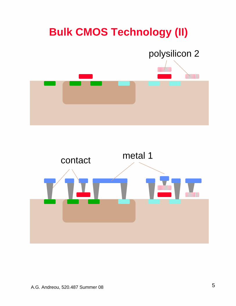
MicroElectroMechanical Systems (MEMS)
• MEMS• MEMS before CMOS
– Analog Devices i-MEMSProcess mechanical structures before
CMOS.• MEMS after CMOS
– Berkeley SiGe MEMSProcess mechanical structures after
CMOS being careful not to affect CMOS
• MEMS in CMOS– Post-processing Bulk CMOS
(Fedder, Carnegie Mellon)– Post-processing SOI CMOS

A.G. Andreou, 520.487 Summer 08 15
MUMP(MultiUser MEMS Process)
• PolyMUMP: 3 layer polysilicon surface micromachining
• SOIMUMP: 3 mask Silicon On Insulator bulk micromachining
• MetalMUMP: electroplated nickel process.
• ASIMPS: MEMS on CMOS using Jazz SiGe CMOS technology
This course will teach you how to design Microsystems (MEMS) in foundry technologies!
Key idea: Use a series of functional layers combined with sacrificial layers to produced desired structures
http://www.memscap.com/en_mumps.html

A.G. Andreou, 520.487 Summer 08 16
MUMPS Surface Micromachining
A.G. Andreou, 520.487 Summer 08 17
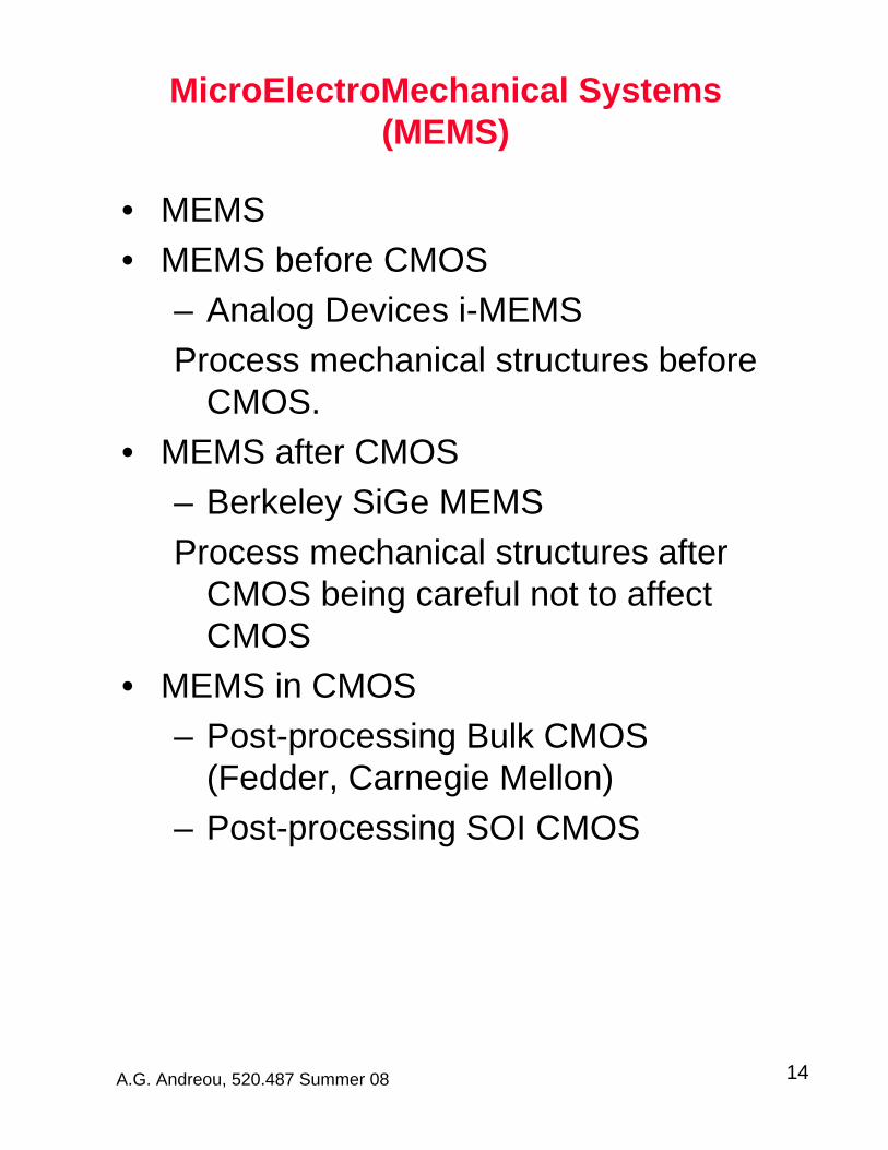
Spinning Gear
A.G. Andreou, 520.487 Summer 08 18
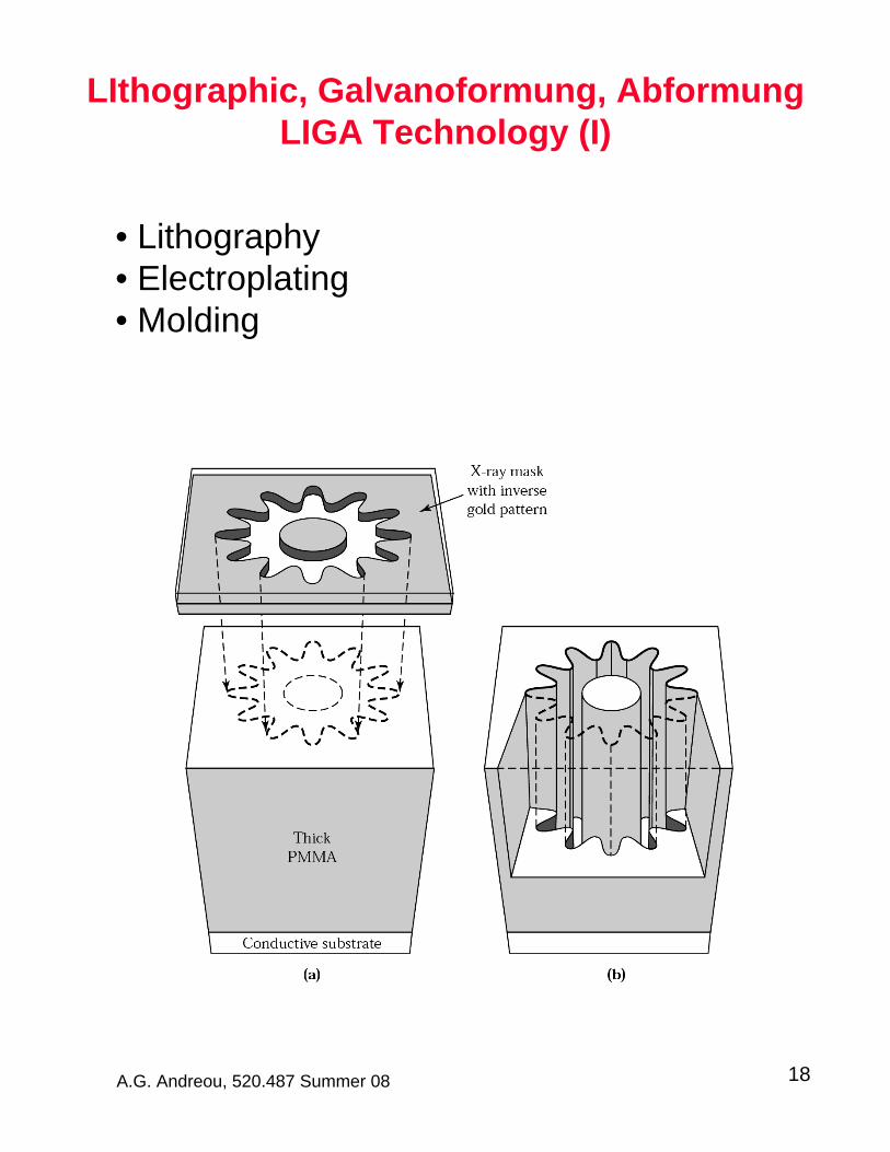
LIthographic, Galvanoformung, AbformungLIGA Technology (I)
• Lithography• Electroplating• Molding

A.G. Andreou, 520.487 Summer 08 19
LIGA Process (II)
THICK 10um to 1mm MICROSTRUCTURES

A.G. Andreou, 520.487 Summer 08 20
MEMS with SOI-CMOS
• Build CMOS MEMS structures using stacked metal and oxide layers
• Release steps– Step 1 vertical etch down to
sapphire substrate
– Step 2 lateral sacrificial release layer etch to free MEMS
A.G. Andreou, 520.487 Summer 08 21
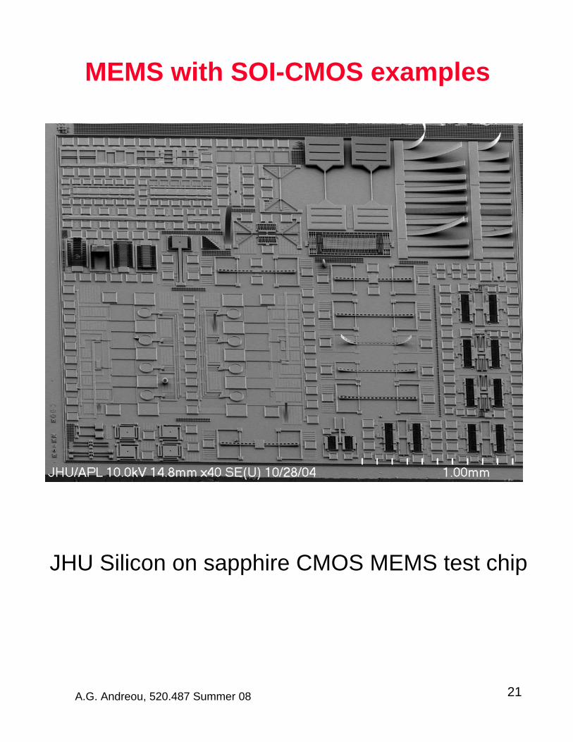
MEMS with SOI-CMOS examples
JHU Silicon on sapphire CMOS MEMS test chip


![Temperature compensation model of MEMS inertial …inertial sensors that are fabricated with their electronic circuits and other mechanical components on a common substrate [1]. MEMS-based](https://img.pdfslide.us/doc/110x75/5e58fefc43d5e4795f258b2f/temperature-compensation-model-of-mems-inertial-inertial-sensors-that-are-fabricated.jpg)