Embed Size (px)
Citation preview
FEATURES
Fast access time : 55ns Low power consumption: Operating current : 30mA (TYP.)Standby current : 6µA (TYP.) LL-version
Single 2.7V ~ 5.5V power supply All inputs and outputs TTL compatible Fully static operation Tri-state output Data byte control : LB# (DQ0 ~ DQ7)
UB# (DQ8 ~ DQ15) Data retention voltage : 1.5V (MIN.)
Lead free and green package available Package : 44-pin 400 mil TSOP-II
48-ball 6mm x 8mm TFBGA
GENERAL DESCRIPTION
The AS6C8016 is a 8,388,608-bit low power CMOS static random access memory organized as 524,288 words by 16 bits. It is fabricated using very high performance, high reliability CMOS technology. Its standby current is stable within the range of operating temperature.
The AS6C8016 is well designed for low power application, and particularly well suited for battery back-up nonvolatile memory application.
The AS6C8016 operates from a single power supply of 2.7V ~ 5.5V and all inputs and outputs are fully TTL compatible
PRODUCT FAMILY
Power Dissipation Product Family
OperatingTemperature Vcc Range Speed
Standby(ISB1,TYP.) Operating(Icc,TYP.)AS6C8016(I) -40 ~ 85℃ 2.7 ~ 5.5V 55ns 6µA(LL) 30mA
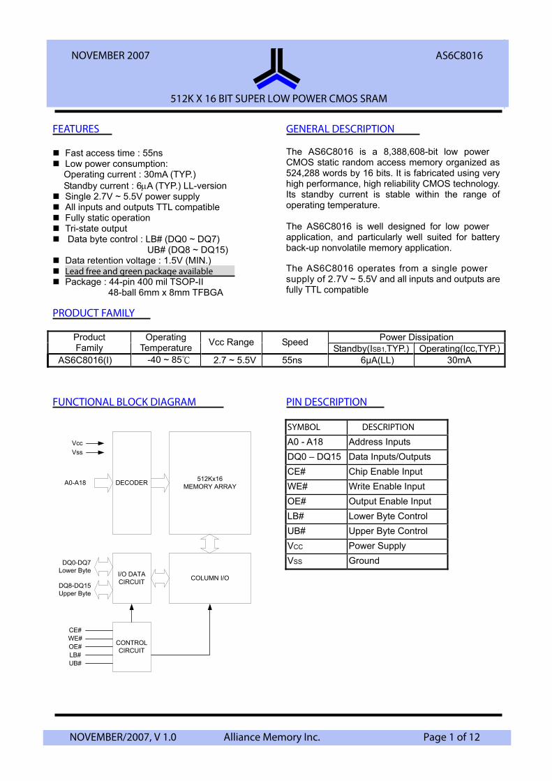
FUNCTIONAL BLOCK DIAGRAM
CONTROLCIRCUIT
CE#WE#OE#
DECODER 512Kx16MEMORY ARRAY
COLUMN I/O
A0-A18
VccVss
DQ8-DQ15Upper Byte
DQ0-DQ7Lower Byte I/O DATA
CIRCUIT
LB#UB#
PIN DESCRIPTION
SYMBOL DESCRIPTION
A0 - A18 Address Inputs DQ0 – DQ15 Data Inputs/Outputs CE# Chip Enable Input WE# Write Enable Input OE# Output Enable Input LB# Lower Byte Control UB# Upper Byte Control VCC Power Supply VSS Ground
512K X 8 BIT LOW POWER CMOS SRAM
January 2007NOVEMBER 2007
NOVEMBER/2007, V 1.0 Alliance Memory Inc. Page 1 of 12
AS6C8016
512K X 16 BIT SUPER LOW POWER CMOS SRAM

PIN CONFIGURATION
108
C6S
A6
A1
A2
A3
A4
DQ15DQ0
DQ1
DQ2
Vcc
Vss
A13
A18
DQ14
DQ12
DQ13
DQ11
Vss
Vcc
DQ10
DQ9
DQ3
DQ4
TSOP II
28
14
13
12
11
10
9
8
7
6
5
4
3
2
1
17
16
15
20
19
18
22 23
24
25
26
27
21
A17
A0
DQ6
DQ7
A5
A6
A7
A9
A10
DQ5
DQ8
A16
A15
A14
A11
A8
34
29
30
31
32
33
44
39
40
41
42
43
35
36
37
38
A12
CE#
WE#
LB#
UB#
OE#
TFBGA
NC
A3
A10A9 A11
A0
A14
A8 NC
WE#
DQ9
DQ14
DQ15
A18
Vss
NC
A13
DQ8
Vcc
Vcc
DQ7
A15
Vss
CE#
LB#
DQ6
DQ2
DQ0
A2OE# A1
A6A5
A4UB#
1 2 3 4 5 6
H
G
C
D
E
F
A
B
A12
NC
A17 A7
A16
DQ10
DQ11
DQ12
DQ13 DQ5
DQ4
DQ3
DQ1
ABSOLUTE MAXIMUN RATINGS*
PARAMETER SYMBOL RATING UNIT Voltage on VCC relative to VSS VT1 -0.5 to 6.5 V
Voltage on any other pin relative to VSS VT2 -0.5 to VCC+0.5 V
Operating Temperature TA -40 to 85(I grade) ℃
Storage Temperature TSTG -65 to 150 ℃
Power Dissipation PD 1 W
DC Output Current IOUT 50 mA
Soldering Temperature (under 10 sec) TSOLDER 260 ℃
*Stresses greater than those listed under “Absolute Maximum Ratings” may cause permanent damage to the device. This is a stressrating only and functional operation of the device or any other conditions above those indicated in the operational sections of this specification is not implied. Exposure to the absolute maximum rating conditions for extended period may affect device reliability.
512K X 8 BIT LOW POWER CMOS SRAM
January 2007NOVEMBER 2007
NOVEMBER/2007, V 1.0 Alliance Memory Inc. Page 2 of 12
AS6C8016
512K X 16 BIT SUPER LOW POWER CMOS SRAM
TRUTH TABLE
I/O OPERATION MODE CE# OE# WE# LB# UB#DQ0-DQ7 DQ8-DQ15
SU P PLY CURRENT
Standby HX
XX
XX
XH
XH
High – Z High – Z
High – Z High – Z ISB1
Output Disable LL
HH
HH
LX
XL
High – Z High – Z
High – Z High – Z ICC,ICC1
Read LLL
LLL
HHH
LHL
HLL
DOUTHigh – Z
DOUT
High – Z DOUT DOUT
ICC,ICC1
Write LLL
XXX
LLL
LHL
HLL
DINHigh – Z
DIN
High – Z DINDIN
ICC,ICC1
Note: H = VIH, L = VIL, X = Don't care.
DC ELECTRICAL CHARACTERISTICS
PARAMETER SYMBOL TEST CONDITION MIN. TYP. *4 MAX. UNITSupply Voltage VCC 2.7 3.0 5.5 V Input High Voltage VIH
*1 2.4 - VCC+0.3 V Input Low Voltage VIL
*2 - 0.2 - 0.6 V Input Leakage Current ILI VCC VIN VSS - 1 - 1 µAOutput Leakage Current ILO
VCC VOUT VSS
Output Disabled - 1 - 1 µA
Output High Voltage VOH IOH = -1mA 2.4 2.7 - V Output Low Voltage VOL IOL = 2mA - - 0.4 V
- 55 - 30 60 mAICC
Cycle time = Min. CE# = VIL,II/O = 0mA Other pins at VIL or VIH
Average Operating Power supply Current
ICC1
Cycle time = 1µsCE#≦
≦≦
≦ ≦
≦
0.2V, II/O = 0mA Other pins at 0.2V or VCC-0.2V
- 4 12 mA
Standby Power Supply Current ISB1
CE# VCC-0.2V Other pins at 0.2V or VCC-0.2V
- 6 50 µA
Notes:1. VIH(max) = VCC + 3.0V for pulse width less than 10ns. 2. VIL(min) = VSS - 3.0V for pulse width less than 10ns. 3. Over/Undershoot specifications are characterized, not 100% tested.4. Typical values are included for reference only and are not guaranteed or tested.
Typical valued are measured at VCC = VCC(TYP.) and TA = 25℃
℃CAPACITANCE (T A = 25 , f = 1.0MHz)
PARAMETER SYMBOL MIN. MAX UNIT Input Capacitance CIN - 6 pF Input/Output Capacitance CI/O - 8 pF Note : These parameters are guaranteed by device characterization, but not production tested.
512K X 8 BIT LOW POWER CMOS SRAM
January 2007NOVEMBER 2007
NOVEMBER/2007, V 1.0 Alliance Memory Inc. Page 3 of 12
AS6C8016
512K X 16 BIT SUPER LOW POWER CMOS SRAM
AC TEST CONDITIONS
Input Pulse Levels 0.2V to VCC - 0.2V Input Rise and Fall Times 3ns Input and Output Timing Reference Levels 1.5V Output Load CL = 30pF + 1TTL, IOH/IOL = -1mA/2mA
AC ELECTRICAL CHARACTERISTICS
(1) READ CYCLEAS6C8016PARAMETER SYM. UNIT
Read Cycle Time tRC
Address Access Time tAA
Chip Enable Access Time tACE
Output Enable Access Time tOE
Chip Enable to Output in Low-Z tCLZ
Output Enable to Output in Low-Z tOLZ
Chip Disable to Output in High-Z tCHZ
Output Disable to Output in High-Z tOHZ
Output Hold from Address Change tOH
LB#, UB# Access Time tBA
LB#, UB# to High-Z Output tBHZ
LB#, UB# to Low-Z Output tBLZ
(2) WRITE CYCLEAS6C8016PARAMETER UNIT
Write Cycle Time tWC
Address Valid to End of Write tAW
Chip Enable to End of Write tCW
Address Set-up Time tAS
Write Pulse Width tWP
Write Recovery Time tWR
Data to Write Time Overlap tDW
Data Hold from End of Write Time tDH
Output Active from End of Write tOW
Write to Output in High-Z tWHZ
LB#, UB# Valid to End of Write tBW
*These parameters are guaranteed by device characterization, but not production tested.
512K X 8 BIT LOW POWER CMOS SRAM
January 2007NOVEMBER 2007
NOVEMBER/2007, V 1.0 Alliance Memory Inc. Page 4 of 12
AS6C8016
512K X 16 BIT SUPER LOW POWER CMOS SRAM
SYM.
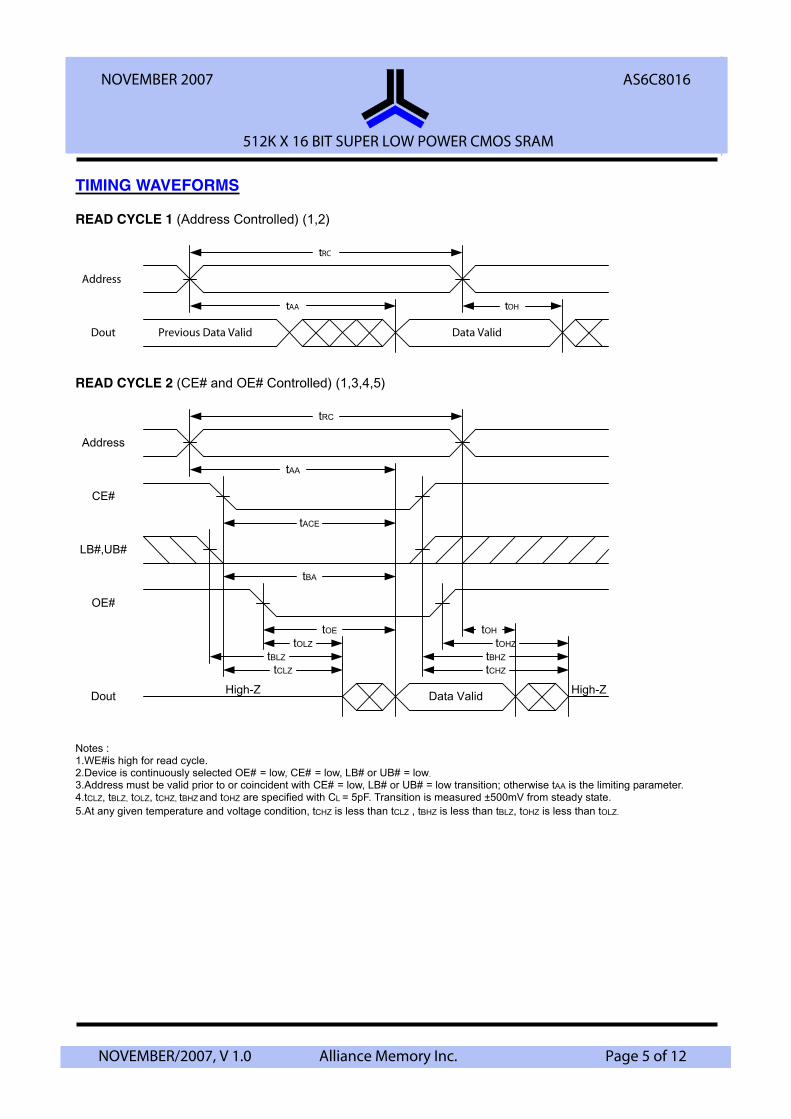
TIMING WAVEFORMS
READ CYCLE 1 (Address Controlled) (1,2)
Dout Data Valid
tOHtAA
Address
tRC
Previous Data Valid
READ CYCLE 2 (CE# and OE# Controlled) (1,3,4,5)
Dout Data ValidHigh-ZHigh-Z
tCLZ
tOLZ
tCHZ
tOHZ
tOH
OE#
tOE
LB#,UB#
tBHZ
tACE
CE#
tAA
Address
tRC
tBA
tBLZ
Notes : 1.WE#is high for read cycle. 2.Device is continuously selected OE# = low, CE# = low, LB# or UB# = low.
3.Address must be valid prior to or coincident with CE# = low, LB# or UB# = low transition; otherwise tAA is the limiting parameter. 4.tCLZ, tBLZ, tOLZ, tCHZ, tBHZ and tOHZ are specified with CL = 5pF. Transition is measured ±500mV from steady state. 5.At any given temperature and voltage condition, tCHZ is less than tCLZ , tBHZ is less than tBLZ, tOHZ is less than tOLZ.
512K X 8 BIT LOW POWER CMOS SRAM
January 2007NOVEMBER 2007
NOVEMBER/2007, V 1.0 Alliance Memory Inc. Page 5 of 12
AS6C8016
512K X 16 BIT SUPER LOW POWER CMOS SRAM
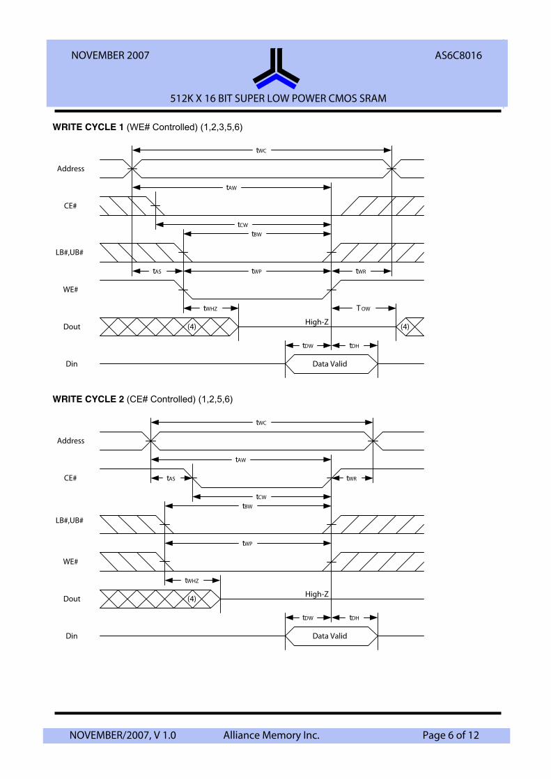
WRITE CYCLE 1 (WE# Controlled) (1,2,3,5,6)
Dout
Din Data Valid
tDW tDH
(4)High-Z
tWHZ
WE#
tWP
tCW
tWRtAS
(4)
T OW
LB#,UB#
CE#
tAW
Address
tWC
tBW
WRITE CYCLE 2 (CE# Controlled) (1,2,5,6)
Dout
Din Data Valid
tDW tDH
(4)High-Z
tWHZ
WE#
LB#,UB#
tCW
CE#
Address
tWRtAS
tAW
tWC
tWP
tBW
512K X 8 BIT LOW POWER CMOS SRAM
January 2007NOVEMBER 2007
NOVEMBER/2007, V 1.0 Alliance Memory Inc. Page 6 of 12
AS6C8016
512K X 16 BIT SUPER LOW POWER CMOS SRAM

WRITE CYCLE 3 (LB#,UB# Controlled) (1,2,5,6)
Dout
Din Data Valid
tDW tDH
(4)High-Z
tWHZ
WE#
LB#,UB#
tCW
CE#
Address
tWR
tAS
tAW
tWC
tWP
tBW
Notes : 1.WE#,CE#, LB#, UB# must be high during all address transitions. 2.A write occurs during the overlap of a low CE#, low WE#, LB# or UB# = low. 3.During a WE# controlled write cycle with OE# low, tWP must be greater than tWHZ + tDW to allow the drivers to turn off and data to be
placed on the bus. 4.During this period, I/O pins are in the output state, and input signals must not be applied. 5.If the CE#, LB#, UB# low transition occurs simultaneously with or after WE# low transition, the outputs remain in a high impedance
state. 6.tOW and tWHZ are specified with CL = 5pF. Transition is measured ±500mV from steady state.
512K X 8 BIT LOW POWER CMOS SRAM
January 2007NOVEMBER 2007
NOVEMBER/2007, V 1.0 Alliance Memory Inc. Page 7 of 12
AS6C8016
512K X 16 BIT SUPER LOW POWER CMOS SRAM
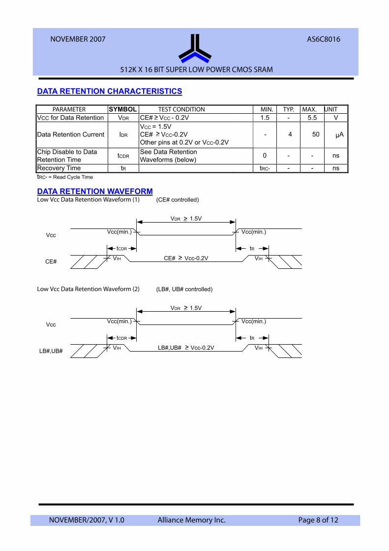
DATA RETENTION CHARACTERISTICS
PARAMETER SYMBOL TEST CONDITION MIN. TYP. MAX. UNITVCC for Data Retention VDR CE# VCC - 0.2V 1.5 - 5.5 V
Data Retention Current IDR
VCC = 1.5V CE# VCC-0.2V Other pins at 0.2V or VCC-0.2V
- 4 50 µA
Chip Disable to Data Retention Time tCDR
See Data Retention Waveforms (below) 0 - - ns
Recovery Time tR tRC* - - ns tRC* = Read Cycle Time
DATA RETENTION WAVEFORMLow Vcc Data Retention Waveform (1) (CE# controlled)
Vcc
CE#
VDR 1.5V
CE# Vcc-0.2V
Vcc(min.)
VIH
tRtCDR
VIH
Vcc(min.)
Low Vcc Data Retention Waveform (2) (LB#, UB# controlled)
Vcc
LB#,UB#
VDR 1.5V
LB#,UB# Vcc-0.2V
Vcc(min.)
VIH
tRtCDR
VIH
Vcc(min.)
512K X 8 BIT LOW POWER CMOS SRAM
January 2007NOVEMBER 2007
NOVEMBER/2007, V 1.0 Alliance Memory Inc. Page 8 of 12
AS6C8016
512K X 16 BIT SUPER LOW POWER CMOS SRAM
>_
>_
>_
>_
>_
>_
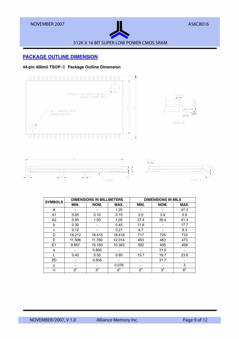
PACKAGE OUTLINE DIMENSION
44-pin 400mil TSOP-ⅡⅡ Package Outline Dimension
θ
DIMENSIONS IN MILLMETERS DIMENSIONS IN MILS SYMBOLS
MIN. NOM. MAX. MIN. NOM. MAX. A - - 1.20 - - 47.2 A1 0.05 0.10 0.15 2.0 3.9 5.9 A2 0.95 1.00 1.05 37.4 39.4 41.3 b 0.30 - 0.45 11.8 - 17.7 c 0.12 - 0.21 4.7 - 8.3 D 18.212 18.415 18.618 717 725 733 E 11.506 11.760 12.014 453 463 473 E1 9.957 10.160 10.363 392 400 408 e - 0.800 - - 31.5 - L 0.40 0.50 0.60 15.7 19.7 23.6
ZD - 0.805 - - 31.7 - y - - 0.076 - - 3 Θ 0o 3o 6o 0o 3o 6o
512K X 8 BIT LOW POWER CMOS SRAM
January 2007NOVEMBER 2007
NOVEMBER/2007, V 1.0 Alliance Memory Inc. Page 9 of 12
A S 6 C 8 0 1 6
512K X 16 BIT SUPER LOW POWER CMOS SRAM
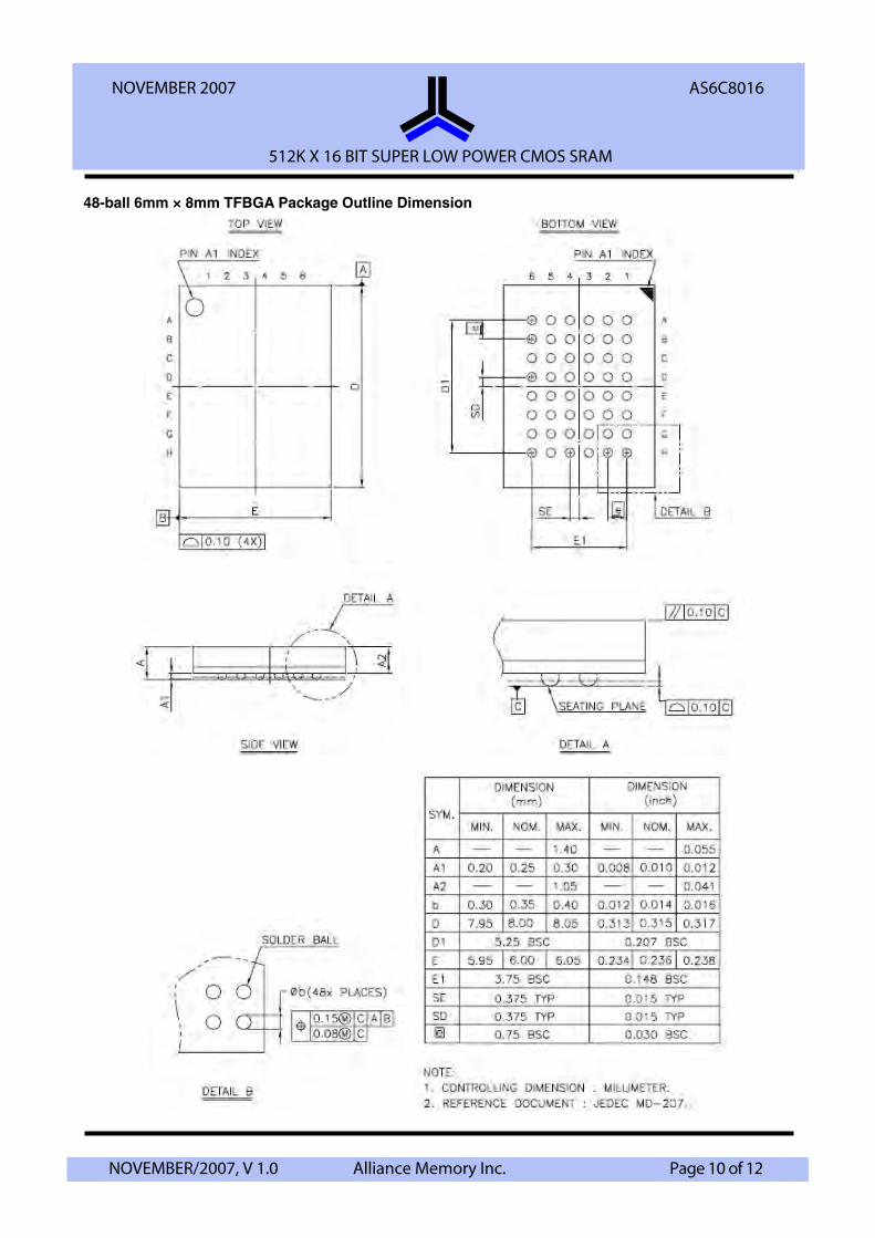
48-ball 6mm × 8mm TFBGA Package Outline Dimension
512K X 8 BIT LOW POWER CMOS SRAM
January 2007NOVEMBER 2007
NOVEMBER/2007, V 1.0 Alliance Memory Inc. Page 10 of 12
AS6C8016
512K X 16 BIT SUPER LOW POWER CMOS SRAM
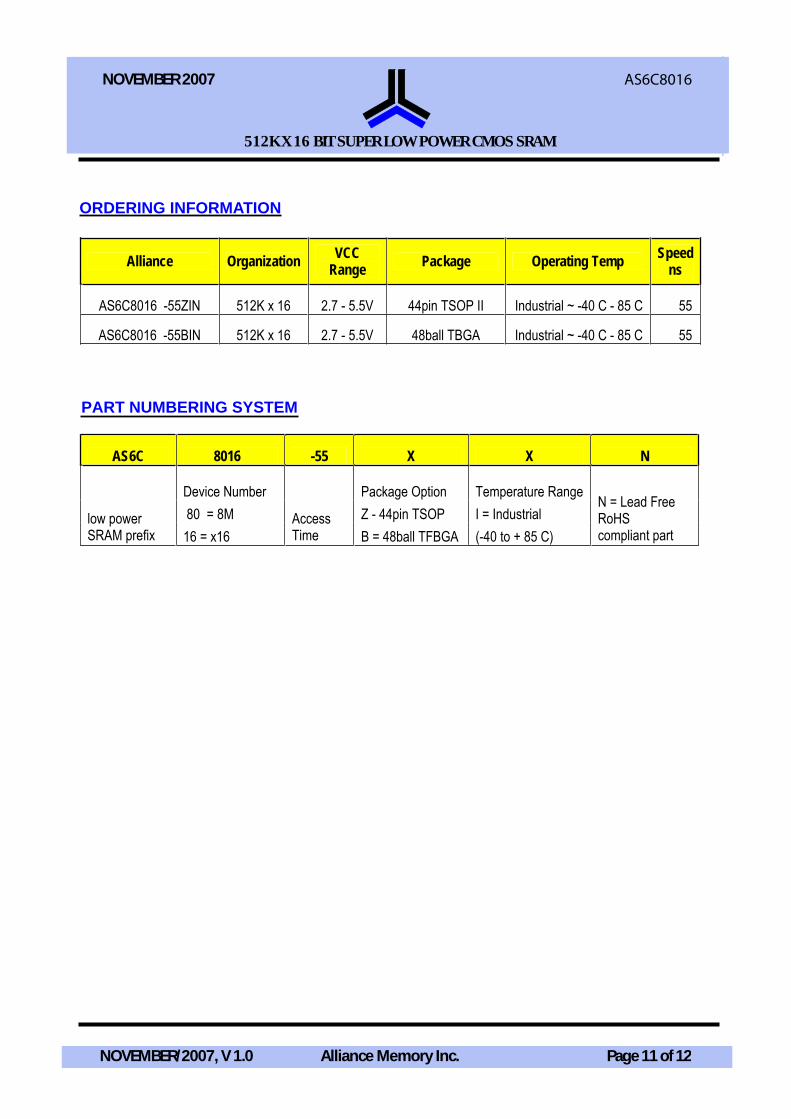
ORDERING INFORMATION
Alliance Organization VCCRange Package Operating Temp Speed
ns
AS6C8016 -55ZIN 512K x 16 2.7 - 5.5V 44pin TSOP II Industrial ~ -40 C - 85 C 55
AS6C8016 -55BIN 512K x 16 2.7 - 5.5V 48ball TBGA Industrial ~ -40 C - 85 C 55
PART NUMBERING SYSTEM
AS6C 8016 -55 X X N
Device Number Package Option Temperature Range 80 = 8M Z - 44pin TSOP I = Industriallow power
SRAM prefix 16 = x16AccessTime B = 48ball TFBGA (-40 to + 85 C)
N = Lead Free RoHScompliant part
512K X 8 BI T LOW POWER CMOS SRAM
January 2007NOVEMBER 2007
NOVEMBER/2007, V 1.0 Alliance Memory Inc. Page 11 of 12
AS6C8016
512K X 16 BIT SUPER LOW POWER CMOS SRAM
Copyright © Alliance Memory
All Rights Reserved
Alliance Memory, Inc511 Taylor Way,San Carlos, CA 94070, USAPhone: 650-610-6800Fax: 650-620-9211
www.alliancememory.com
© Copyright 2007 Alliance Memory, Inc. All rights reserved. Our three-point logo, our name and Intelliwatt are trademarks or registered trademarks ofAlliance. All other brand and product names may be the trademarks of their respective companies. Alliance reserves the right to make changes to thisdocument and its products at any time without notice. Alliance assumes no responsibility for any errors that may appear in this document. The datacontained herein represents Alliance's best data and/or estimates at the time of issuance. Alliance reserves the right to change or correct this data at anytime, without notice. If the product described herein is under development, significant changes to these specifications are possible. The information inthis product data sheet is intended to be general descriptive information for potential customers and users, and is not intended to operate as, or provide,any guarantee or warrantee to any user or customer. Alliance does not assume any responsibility or liability arising out of the application or use of anyproduct described herein, and disclaims any express or implied warranties related to the sale and/or use of Alliance products including liability orwarranties related to fitness for a particular purpose, merchantability, or infringement of any intellectual property rights, except as express agreed to inAlliance's Terms and Conditions of Sale (which are available from Alliance). All sales of Alliance products are made exclusively according to Alliance'sTerms and Conditions of Sale. The purchase of products from Alliance does not convey a license under any patent rights, copyrights; mask works rights,trademarks, or any other intellectual property rights of Alliance or third parties. Alliance does not authorize its products for use as critical components inlife-supporting systems where a malfunction or failure may reasonably be expected to result in significant injury to the user, and the inclusion ofAlliance products in such life-supporting systems implies that the manufacturer assumes all risk of such use and agrees to indemnify Alliance against allclaims arising from such use.
®
512K X 8 BIT LOW POWER CMOS SRAM
January 2007
512K X 16 BIT LOW POWER CMOS SRAM
NOVEMBER 2007 AS6C8016
NOVEMBER/2007, V 1.0 Alliance Memory Inc. Page 12 of 12
![netlusa.comnetlusa.com/desbravadores.pt/images/MANUAIS/Manual_Caes.pdf · ï } / v } µ ] } x x x x x x x x x x x x x x x x x x x x x x x x x x x x x x x x x x x x x x x x x x x x](https://img.pdfslide.us/doc/110x75/5be3717009d3f20a668b6378/-i-v-x-x-x-x-x-x-x-x-x-x-x-x-x-x-x-x-x-x-x-x-x-x-x-x-x-x-x-x-x.jpg)