Embed Size (px)
Citation preview

Document Number: MC33886Rev 10.0, 01/2014
Freescale SemiconductorTechnical Data
5.0 A H-BridgeThe 33886 is a monolithic H-Bridge ideal for fractional horsepower DC-motor and bi-directional thrust solenoid control. The IC incorporates internal control logic, charge pump, gate drive, and low RDS(ON) MOSFET output circuitry. The 33886 is able to control continuous inductive DC load currents up to 5.0 A. Output loads can be pulse width modulated (PWM-ed) at frequencies up to 10 kHz.
A Fault Status output reports undervoltage, short-circuit, and overtemperature conditions. Two independent inputs control the two half-bridge totem-pole outputs. Two disable inputs force the H-Bridge outputs to tri-state (exhibit high-impedance).
The 33886 is parametrically specified over a temperature range of -40 C TA 125 C, 5.0 V V+ 28 V. The IC can also be operated up to 40 V with derating of the specifications. The IC is available in a surface mount power package with exposed pad for heatsinking. This device is powered by SMARTMOS technology.
Features• 5.0 V to 40 V continuous operation• 120 m RDS(on) H-Bridge MOSFETs• TTL / CMOS compatible Inputs• PWM frequencies up to 10 kHz• Active current limiting via internal constant off-time PWM (with
temperature-dependent threshold reduction)• Output short-circuit protection• Undervoltage shutdown• Fault status reporting
Figure 1. 33886 Simplified Application Diagram
H-BRIDGE
VW SUFFIX (PB-FREE)98ASH70702A20-PIN HSOP
33886
Applications
• Automotive systems• DC motor control in industrial and robotic systems• DC motor and actuator control in boats, RVs, and
marine systems• Appliance and white goods electrical actuators• Powered machine and hand tools• Antenna rotors and dish positioning systems
MCUIN
OUTOUT
OUT
OUT
5.0 V33886
CCP V+
IN1IN2
D1
D2 GND
OUT2
OUT1
PGND
FS
Motor
V+
© Freescale Semiconductor, Inc., 2007 - 2014. All rights reserved.
1 Orderable Parts
Table 1. Orderable Part Variations
Part Number Temperature (TA) Package
MC33886PVW/R2 -40 to 125 °C 20 HSOP
Analog Integrated Circuit Device Data2 Freescale Semiconductor
33886
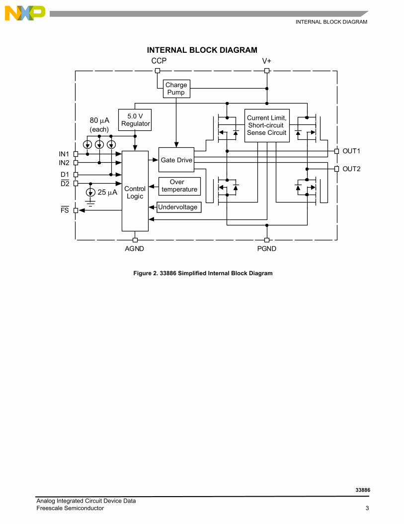
INTERNAL BLOCK DIAGRAM
INTERNAL BLOCK DIAGRAM
Figure 2. 33886 Simplified Internal Block Diagram
ChargePump
Over-temperature
5.0 VRegulator
Gate Drive
Current Limit,Overcurrent
SenseCircuit
Undervoltage
OUT1
OUT2
IN1IN2
D1D2
FS
CCP VPWR
PGNDAGND
ControlLogic
80 uA(each)
25 uA
80 A
25 A
Current Limit,Short-circuitSense Circuit
ChargePump
5.0 VRegulator
Gate Drive
Overtemperature
V+CCP
Undervoltage
Analog Integrated Circuit Device DataFreescale Semiconductor 3
33886
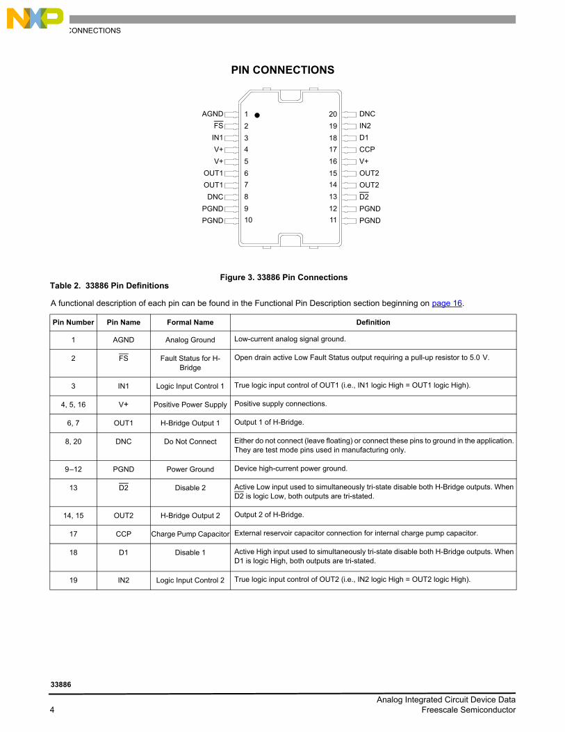
PIN CONNECTIONS
PIN CONNECTIONS
Figure 3. 33886 Pin ConnectionsTable 2. 33886 Pin Definitions
A functional description of each pin can be found in the Functional Pin Description section beginning on page 16.
Pin Number Pin Name Formal Name Definition
1 AGND Analog Ground Low-current analog signal ground.
2 FS Fault Status for H-Bridge
Open drain active Low Fault Status output requiring a pull-up resistor to 5.0 V.
3 IN1 Logic Input Control 1 True logic input control of OUT1 (i.e., IN1 logic High = OUT1 logic High).
4, 5, 16 V+ Positive Power Supply Positive supply connections.
6, 7 OUT1 H-Bridge Output 1 Output 1 of H-Bridge.
8, 20 DNC Do Not Connect Either do not connect (leave floating) or connect these pins to ground in the application. They are test mode pins used in manufacturing only.
9 –12 PGND Power Ground Device high-current power ground.
13 D2 Disable 2 Active Low input used to simultaneously tri-state disable both H-Bridge outputs. When D2 is logic Low, both outputs are tri-stated.
14, 15 OUT2 H-Bridge Output 2 Output 2 of H-Bridge.
17 CCP Charge Pump Capacitor External reservoir capacitor connection for internal charge pump capacitor.
18 D1 Disable 1 Active High input used to simultaneously tri-state disable both H-Bridge outputs. When D1 is logic High, both outputs are tri-stated.
19 IN2 Logic Input Control 2 True logic input control of OUT2 (i.e., IN2 logic High = OUT2 logic High).
DNCAGND
IN2
D1
CCP
V+
OUT2
OUT2
D2
PGND
PGND
FS
V+
OUT1
OUT1
DNC
PGND
PGND
IN1
V+
1
2
3
4
5
6
7
8
9
10
20
19
16
15
14
13
12
11
18
17
Analog Integrated Circuit Device Data4 Freescale Semiconductor
33886
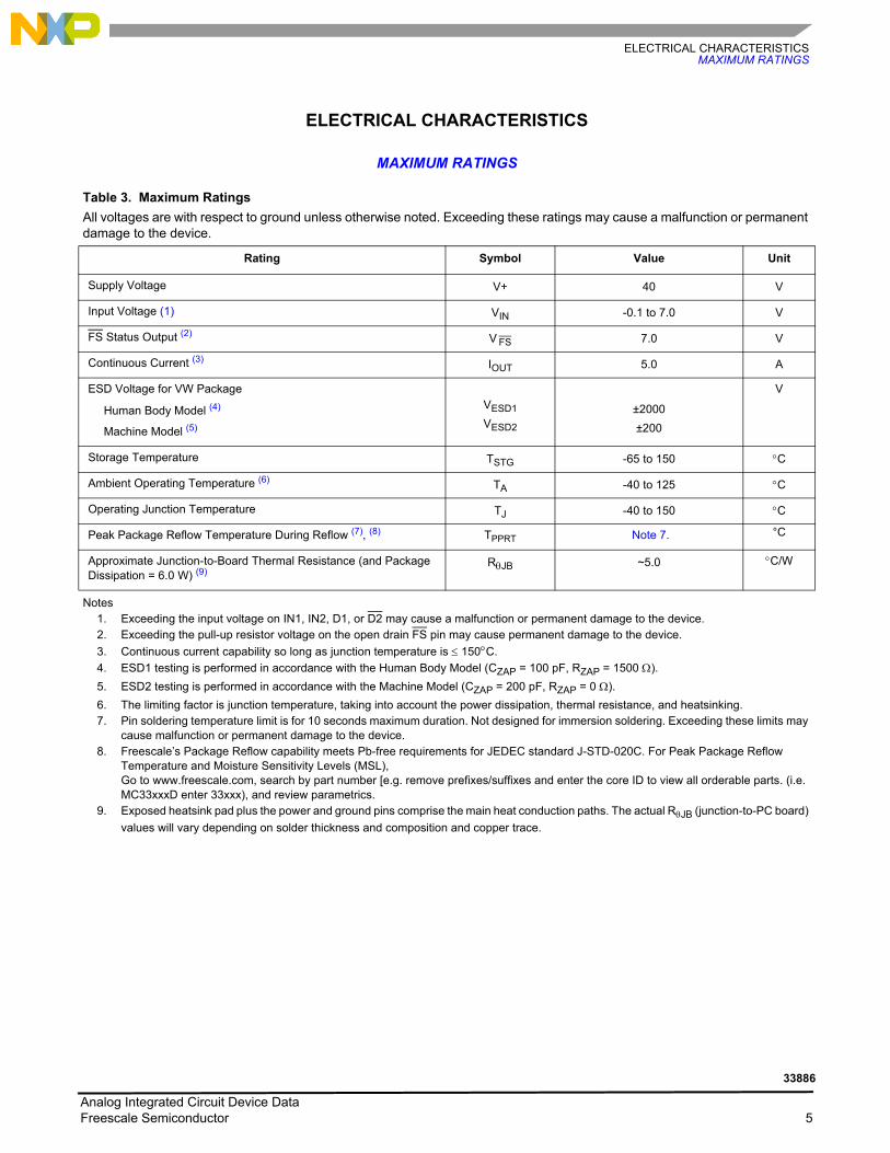
ELECTRICAL CHARACTERISTICSMAXIMUM RATINGS
ELECTRICAL CHARACTERISTICS
MAXIMUM RATINGS
Table 3. Maximum Ratings
All voltages are with respect to ground unless otherwise noted. Exceeding these ratings may cause a malfunction or permanent damage to the device.
Rating Symbol Value Unit
Supply Voltage V+ 40 V
Input Voltage (1) VIN -0.1 to 7.0 V
FS Status Output (2) V FS 7.0 V
Continuous Current (3) IOUT 5.0 A
ESD Voltage for VW Package
Human Body Model (4)
Machine Model (5)
VESD1
VESD2
±2000
±200
V
Storage Temperature TSTG -65 to 150 C
Ambient Operating Temperature (6) TA -40 to 125 C
Operating Junction Temperature TJ -40 to 150 C
Peak Package Reflow Temperature During Reflow (7), (8) TPPRT Note 7. °C
Approximate Junction-to-Board Thermal Resistance (and Package Dissipation = 6.0 W) (9)
RJB ~5.0 C/W
Notes1. Exceeding the input voltage on IN1, IN2, D1, or D2 may cause a malfunction or permanent damage to the device.2. Exceeding the pull-up resistor voltage on the open drain FS pin may cause permanent damage to the device.
3. Continuous current capability so long as junction temperature is 150C.
4. ESD1 testing is performed in accordance with the Human Body Model (CZAP = 100 pF, RZAP = 1500 ).
5. ESD2 testing is performed in accordance with the Machine Model (CZAP = 200 pF, RZAP = 0 ).
6. The limiting factor is junction temperature, taking into account the power dissipation, thermal resistance, and heatsinking.7. Pin soldering temperature limit is for 10 seconds maximum duration. Not designed for immersion soldering. Exceeding these limits may
cause malfunction or permanent damage to the device.8. Freescale’s Package Reflow capability meets Pb-free requirements for JEDEC standard J-STD-020C. For Peak Package Reflow
Temperature and Moisture Sensitivity Levels (MSL),Go to www.freescale.com, search by part number [e.g. remove prefixes/suffixes and enter the core ID to view all orderable parts. (i.e. MC33xxxD enter 33xxx), and review parametrics.
9. Exposed heatsink pad plus the power and ground pins comprise the main heat conduction paths. The actual RJB (junction-to-PC board)
values will vary depending on solder thickness and composition and copper trace.
Analog Integrated Circuit Device DataFreescale Semiconductor 5
33886
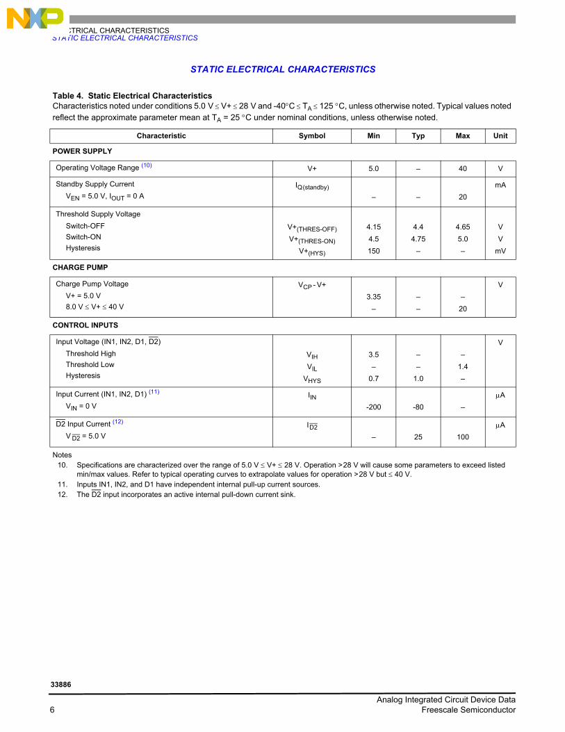
ELECTRICAL CHARACTERISTICSSTATIC ELECTRICAL CHARACTERISTICS
STATIC ELECTRICAL CHARACTERISTICS
Table 4. Static Electrical CharacteristicsCharacteristics noted under conditions 5.0 V V+ 28 V and -40C TA 125C, unless otherwise noted. Typical values noted reflect the approximate parameter mean at TA = 25 C under nominal conditions, unless otherwise noted.
Characteristic Symbol Min Typ Max Unit
POWER SUPPLY
Operating Voltage Range (10) V+ 5.0 – 40 V
Standby Supply Current
VEN = 5.0 V, IOUT = 0 A
IQ (standby)
– – 20
mA
Threshold Supply Voltage
Switch-OFF
Switch-ON
Hysteresis
V+(THRES-OFF)
V+(THRES-ON)
V+(HYS)
4.15
4.5
150
4.4
4.75
–
4.65
5.0
–
V
V
mV
CHARGE PUMP
Charge Pump Voltage
V+ = 5.0 V
8.0 V V+ 40 V
VCP - V+
3.35
–
–
–
–
20
V
CONTROL INPUTS
Input Voltage (IN1, IN2, D1, D2)
Threshold High
Threshold Low
Hysteresis
VIH
VIL
VHYS
3.5
–
0.7
–
–
1.0
–
1.4
–
V
Input Current (IN1, IN2, D1) (11)
VIN = 0 V
IIN-200 -80 –
A
D2 Input Current (12)
V D2 = 5.0 V
I D2
– 25 100
A
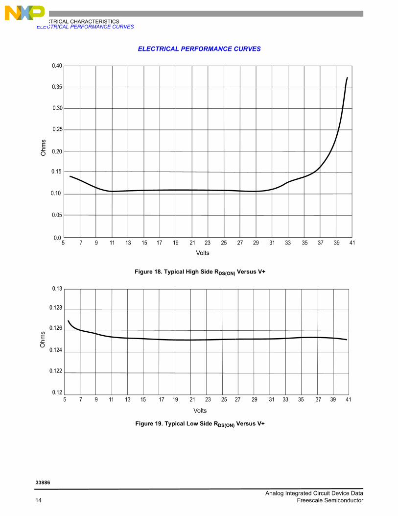
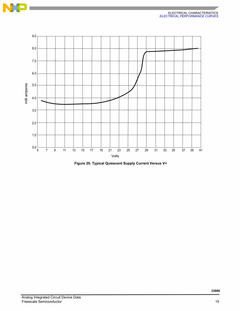
Notes10. Specifications are characterized over the range of 5.0 V V+ 28 V. Operation > 28 V will cause some parameters to exceed listed
min/max values. Refer to typical operating curves to extrapolate values for operation > 28 V but 40 V.11. Inputs IN1, IN2, and D1 have independent internal pull-up current sources.12. The D2 input incorporates an active internal pull-down current sink.
Analog Integrated Circuit Device Data6 Freescale Semiconductor
33886
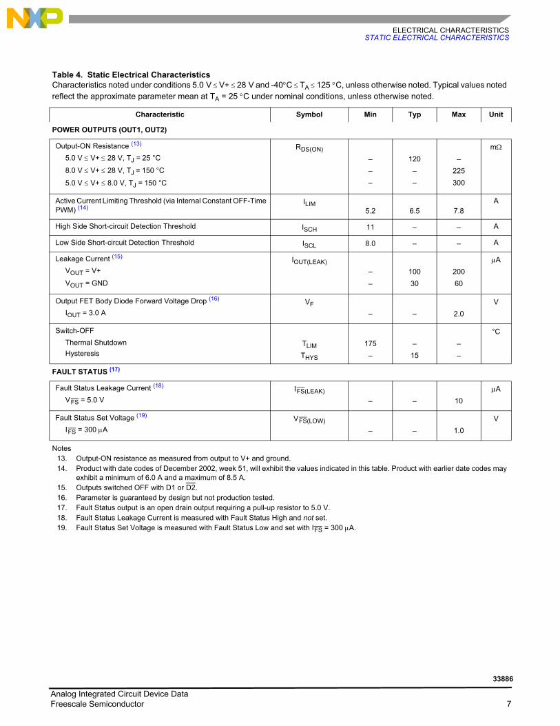
ELECTRICAL CHARACTERISTICSSTATIC ELECTRICAL CHARACTERISTICS
POWER OUTPUTS (OUT1, OUT2)
Output-ON Resistance (13)
5.0 V V+ 28 V, TJ = 25 °C
8.0 V V+ 28 V, TJ = 150 °C
5.0 V V+ 8.0 V, TJ = 150 °C
RDS(ON)
–
–
–
120
–
–
–
225
300
m
Active Current Limiting Threshold (via Internal Constant OFF-Time PWM) (14)
ILIM5.2 6.5 7.8
A
High Side Short-circuit Detection Threshold ISCH 11 – – A
Low Side Short-circuit Detection Threshold ISCL 8.0 – – A
Leakage Current (15)
VOUT = V+
VOUT = GND
IOUT(LEAK)
–
–
100
30
200
60
A
Output FET Body Diode Forward Voltage Drop (16)
IOUT = 3.0 A
VF
– – 2.0
V
Switch-OFF
Thermal Shutdown
HysteresisTLIM
THYS
175
–
–
15
–
–
°C
FAULT STATUS (17)
Fault Status Leakage Current (18)
V FS = 5.0 V
I FS(LEAK)
– – 10
A
Fault Status Set Voltage (19)
I FS = 300 A
V FS(LOW)
– – 1.0
V
Notes13. Output-ON resistance as measured from output to V+ and ground.14. Product with date codes of December 2002, week 51, will exhibit the values indicated in this table. Product with earlier date codes may
exhibit a minimum of 6.0 A and a maximum of 8.5 A.15. Outputs switched OFF with D1 or D2.16. Parameter is guaranteed by design but not production tested.17. Fault Status output is an open drain output requiring a pull-up resistor to 5.0 V.18. Fault Status Leakage Current is measured with Fault Status High and not set.19. Fault Status Set Voltage is measured with Fault Status Low and set with I FS = 300 A.
Table 4. Static Electrical CharacteristicsCharacteristics noted under conditions 5.0 V V+ 28 V and -40C TA 125C, unless otherwise noted. Typical values noted reflect the approximate parameter mean at TA = 25 C under nominal conditions, unless otherwise noted.
Characteristic Symbol Min Typ Max Unit
Analog Integrated Circuit Device DataFreescale Semiconductor 7
33886
ELECTRICAL CHARACTERISTICSDYNAMIC ELECTRICAL CHARACTERISTICS
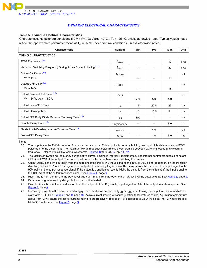
DYNAMIC ELECTRICAL CHARACTERISTICS
Table 5. Dynamic Electrical CharacteristicsCharacteristics noted under conditions 5.0 V V+ 28 V and -40C TA 125 C, unless otherwise noted. Typical values noted reflect the approximate parameter mean at TA = 25 C under nominal conditions, unless otherwise noted.
Characteristic Symbol Min Typ Max Unit
TIMING CHARACTERISTICS
PWM Frequency (20) f PWM – – 10 kHz
Maximum Switching Frequency During Active Current Limiting (21) f MAX – – 20 kHz
Output ON Delay (22)
V+ = 14 V
t d (ON)
– – 18
s
Output OFF Delay (22)
V+ = 14 V
t D (OFF)
– – 18
s
Output Rise and Fall Time (23)
V+ = 14 V, IOUT = 3.0 A
tF , t R2.0 5.0 8.0
s
Output Latch-OFF Time t A 15 20.5 26 s
Output Blanking Time t B 12 16.5 21 s
Output FET Body Diode Reverse Recovery Time (24) t R R 100 – – ns
Disable Delay Time (25) t D (DISABLE) – – 8.0 s
Short-circuit / Overtemperature Turn-OFF Time (26) t FAULT – 4.0 – s
Power-OFF Delay Time t POD – 1.0 5.0 ms
Notes20. The outputs can be PWM controlled from an external source. This is typically done by holding one input high while applying a PWM
pulse train to the other input. The maximum PWM frequency obtainable is a compromise between switching losses and switching frequency. Refer to Typical Switching Waveforms, Figures 10 through 17, pp. 11–12.
21. The Maximum Switching Frequency during active current limiting is internally implemented. The internal control produces a constant OFF-time PWM of the output. The output load current effects the Maximum Switching Frequency.
22. Output Delay is the time duration from the midpoint of the IN1 or IN2 input signal to the 10% or 90% point (dependent on the transition direction) of the OUT1 or OUT2 signal. If the output is transitioning High-to-Low, the delay is from the midpoint of the input signal to the 90% point of the output response signal. If the output is transitioning Low-to-High, the delay is from the midpoint of the input signal to the 10% point of the output response signal. See Figure 4, page 9.
23. Rise Time is from the 10% to the 90% level and Fall Time is from the 90% to the 10% level of the output signal. See Figure 6, page 9.24. Parameter is guaranteed by design but not production tested.25. Disable Delay Time is the time duration from the midpoint of the D (disable) input signal to 10% of the output tri-state response. See
Figure 5, page 9.26. Increasing currents will become limited at ILIM. Hard shorts will breach the ISCH or ISCL limit, forcing the output into an immediate tri-
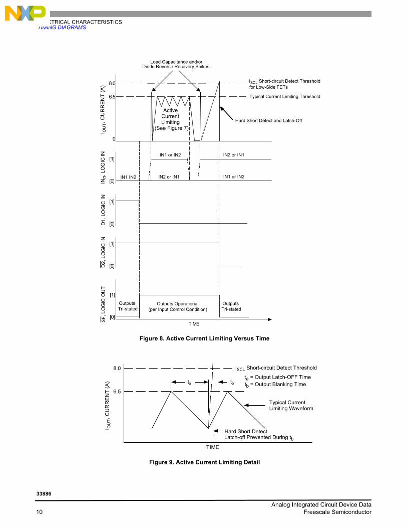
state latch-OFF. See Figures 8 and 9, page 10. Active current limiting will cause junction temperatures to rise. A junction temperature above 160 C will cause the active current limiting to progressively “fold-back” (or decrease) to 2.5 A typical at 175 C where thermal latch-OFF will occur. See Figure 7, page 9.
Analog Integrated Circuit Device Data8 Freescale Semiconductor
33886
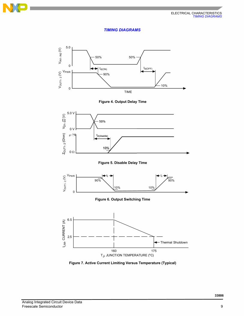
ELECTRICAL CHARACTERISTICSTIMING DIAGRAMS
TIMING DIAGRAMS
Figure 4. Output Delay Time
Figure 5. Disable Delay Time
Figure 6. Output Switching Time
Figure 7. Active Current Limiting Versus Temperature (Typical)
TIME
0
5.0
0
VPWR
td(ON)
50%
90%
50%
10%
VIN
1,IN
2(V
)
td(OFF)
VO
UT
1,
2(V
)
0 V
5.0 V
0
tr
0
VPWR
90%
10%
VO
UT
1,
2(V
)
10%
90%
tf
I MA
X,O
UT
PU
TC
UR
RE
NT
(A)
6.6
2.5
160 175
Thermal Shutdown
TJ, JUNCTION TEMPERATURE (oC)
I LIM
,
6.5
I LIM
, CU
RR
EN
T (
A)
Analog Integrated Circuit Device DataFreescale Semiconductor 9
33886
ELECTRICAL CHARACTERISTICSTIMING DIAGRAMS
Figure 8. Active Current Limiting Versus Time
Figure 9. Active Current Limiting Detail
D1,
LOG
ICIN
[0]
[1]
Hard ShortDetectand Latch-OFF
Typ. Short Ckt. Detect Threshold
PWMCurrentLimiting
(See Figure 6)
8.0
6.5I L
OA
D,O
UTP
UT
CU
RR
EN
T(A
)F
S,L
OG
ICO
UT
OutputsTristated
TIME
D2,
LOG
ICIN
[0]
[0]
[1]
[1]
INn,
LOG
ICIN
[0]
[1]
IN1 IN2
IN2IN1
Outputs Operational(per Input Control Condition)
0
Typ. Current Limit Threshold
OutputsTristated
IN2 IN1OR
OR IN1ORIN2
IN2ORIN1
Diode ReverseRecovery Spikes
(See Figure 7)
ISCL Short-circuit Detect Thresholdfor Low-Side FETs
Typical Current Limiting Threshold
Load Capacitance and/orDiode Reverse Recovery Spikes
Hard Short Detect and Latch-Off
IN1 or IN2 IN2 or IN1
IN1 or IN2IN2 or IN1IN1 IN2
OutputsTri-stated
OutputsTri-stated
Outputs Operational(per Input Control Condition)
SF
I OU
T,
ActiveCurrentLimiting
(See Figure 7)
I OU
T, C
UR
RE
NT
(A
)
Overcurrent Minimum Threshold
ta tb
8.0
TIME
I LO
AD,O
UT
PU
TC
UR
RE
NT
(A)
Typical PWM LoadCurrent LimitingWaveform
Hard OutputShort Latch-OFF
ta = Tristate Output OFF Timetb = Current Limit Blank Time
6.5
Hard Short DetectLatch-off Prevented During tb
Short Circuit Detect Threshold
ta = Output Latch-OFF Timetb = Output Blanking Time
ISCL Short-circuit Detect Threshold
I OU
T, C
UR
RE
NT
(A
)
Typical CurrentLimiting Waveform
Analog Integrated Circuit Device Data10 Freescale Semiconductor
33886
ELECTRICAL CHARACTERISTICSTYPICAL SWITCHING WAVEFORMS
TYPICAL SWITCHING WAVEFORMS
Important For all plots, the following applies:
• Ch2 = 2.0 A per division• LLOAD = 533 H @ 1.0 kHz• LLOAD = 530 H @ 10.0 kHz• RLOAD = 4.0
Figure 10. Output Voltage and Current vs. Input Voltage at V+ = 24 V, PMW Frequency of 1.0 kHz,
and Duty Cycle of 10%
Figure 11. Output Voltage and Current vs. Input Voltage at V+ = 24 V, PMW Frequency of 1.0 kHz,
and Duty Cycle of 50%
Figure 12. Output Voltage and Current vs. Input Voltage at V+ = 34 V, PMW Frequency of 1.0 kHz,
and Duty Cycle of 90%, Showing Device inCurrent Limiting Mode
Figure 13. Output Voltage and Current vs. Input Voltage at V+ = 22 V, PMW Frequency of 1.0 kHz,
and Duty Cycle of 90%
V+=24 V fPWM=1.0 kHz Duty Cycle=10%
IOUT
Output Voltage(OUT1)
Input Voltage (IN1)
V+=24 V fPWM=1.0 kHz Duty Cycle=50%
IOUT
Output Voltage(OUT1)
Input Voltage (IN1)
V+=34 V fPWM=1.0 kHz Duty Cycle=90%
Output Voltage(OUT1)
IOUT
Input Voltage (IN1)
V+=22 V fPWM=1.0 kHz Duty Cycle=90%
IOUT
Output Voltage(OUT1)
Input Voltage (IN1)
Analog Integrated Circuit Device DataFreescale Semiconductor 11
33886
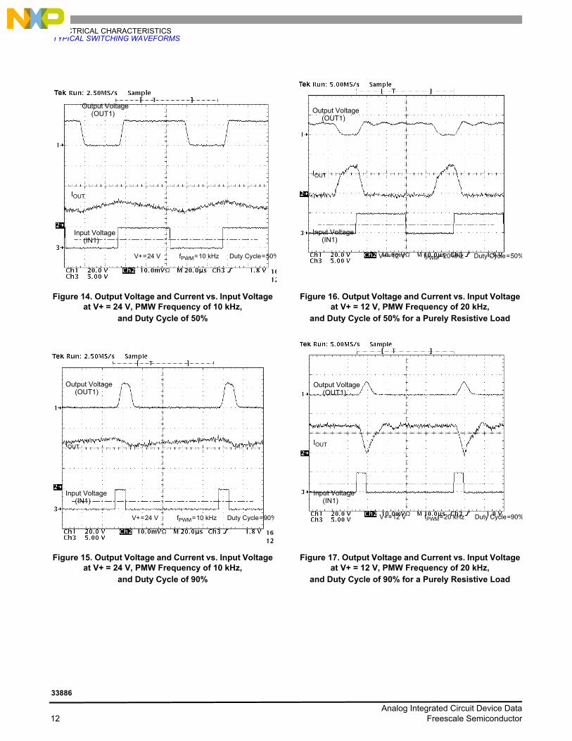
ELECTRICAL CHARACTERISTICSTYPICAL SWITCHING WAVEFORMS
Figure 14. Output Voltage and Current vs. Input Voltage at V+ = 24 V, PMW Frequency of 10 kHz,
and Duty Cycle of 50%
Figure 15. Output Voltage and Current vs. Input Voltage at V+ = 24 V, PMW Frequency of 10 kHz,
and Duty Cycle of 90%
Figure 16. Output Voltage and Current vs. Input Voltage at V+ = 12 V, PMW Frequency of 20 kHz,
and Duty Cycle of 50% for a Purely Resistive Load
Figure 17. Output Voltage and Current vs. Input Voltage at V+ = 12 V, PMW Frequency of 20 kHz,
and Duty Cycle of 90% for a Purely Resistive Load
V+=24 V fPWM=10 kHz Duty Cycle=50%
Output Voltage(OUT1)
IOUT
Input Voltage(IN1)
V+=24 V fPWM=10 kHz Duty Cycle=90%
Output Voltage(OUT1)
IOUT
Input Voltage(IN1)
V+=12 V fPWM=20 kHz Duty Cycle=50%
Output Voltage(OUT1)
IOUT
Input Voltage(IN1)
V+=12 V fPWM=20 kHz Duty Cycle=90%
Output Voltage(OUT1)
IOUT
Input Voltage(IN1)
Analog Integrated Circuit Device Data12 Freescale Semiconductor
33886
ELECTRICAL CHARACTERISTICSTYPICAL SWITCHING WAVEFORMS
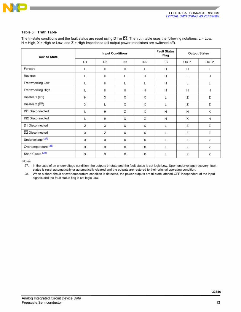
Table 6. Truth Table
The tri-state conditions and the fault status are reset using D1 or D2. The truth table uses the following notations: L = Low, H = High, X = High or Low, and Z = High-impedance (all output power transistors are switched off).
Device StateInput Conditions
Fault Status Flag
Output States
D1 D2 IN1 IN2 FS OUT1 OUT2
Forward L H H L H H L
Reverse L H L H H L H
Freewheeling Low L H L L H L L
Freewheeling High L H H H H H H
Disable 1 (D1) H X X X L Z Z
Disable 2 (D2) X L X X L Z Z
IN1 Disconnected L H Z X H H X
IN2 Disconnected L H X Z H X H
D1 Disconnected Z X X X L Z Z
D2 Disconnected X Z X X L Z Z
Undervoltage (27) X X X X L Z Z
Overtemperature (28) X X X X L Z Z
Short Circuit (28) X X X X L Z Z
Notes27. In the case of an undervoltage condition, the outputs tri-state and the fault status is set logic Low. Upon undervoltage recovery, fault
status is reset automatically or automatically cleared and the outputs are restored to their original operating condition.28. When a short-circuit or overtemperature condition is detected, the power outputs are tri-state latched-OFF independent of the input
signals and the fault status flag is set logic Low.
Analog Integrated Circuit Device DataFreescale Semiconductor 13
33886
ELECTRICAL CHARACTERISTICSELECTRICAL PERFORMANCE CURVES
ELECTRICAL PERFORMANCE CURVES
Figure 18. Typical High Side RDS(ON) Versus V+
Figure 19. Typical Low Side RDS(ON) Versus V+
5 9 117 13 15 19 3733 35 3927 412917 21 23 25 310.0
0.05
0.10
0.15
0.20
0.25
0.30
0.35
0.40
Volts
Ohm
s
5 9 117 13 15 19 3733 35 3927 412917 21 23 25 31
0.13
0.128
0.126
0.124
0.122
0.12
OH
MS
VPWR
Ohm
s
Volts
Analog Integrated Circuit Device Data14 Freescale Semiconductor
33886
ELECTRICAL CHARACTERISTICSELECTRICAL PERFORMANCE CURVES
Figure 20. Typical Quiescent Supply Current Versus V+
5 9 117 13 15 19 3733 35 3927 412917 21 23 25 31
5.0
4.0
3.0
2.0
1.0
0.0
OH
MS
VPWR
6.0
7.0
8.0
9.0
mill
i am
pere
s
Volts
Analog Integrated Circuit Device DataFreescale Semiconductor 15
33886
FUNCTIONAL DESCRIPTIONINTRODUCTION
FUNCTIONAL DESCRIPTION
INTRODUCTION
Numerous protection and operational features (speed, torque, direction, dynamic braking, and PWM control), in addition to the 5.0 A current capability, make the 33886 a very attractive, cost-effective solution for controlling a broad range of fractional horsepower DC motors. A pair of 33886 devices can be used to control bipolar stepper motors in both directions. In addition, the 33886 can be used to control permanent magnet solenoids in a push-pull variable force fashion using PWM control. The 33886 can also be used to excite transformer primary windings with a switched square wave to produce secondary winding AC currents.
As shown in Figure 2, Simplified Internal Block Diagram, page 3, the 33886 is a fully protected monolithic H-Bridge with Fault Status reporting. For a DC motor to run the input conditions need be as follows: D1 input logic Low, D2 input logic High, FS flag cleared (logic High), with one IN logic Low and the other IN logic High to define output polarity. The 33886 can execute dynamic braking by simultaneously turning on either both high side MOSFETs or both low side MOSFETs in the output H-Bridge; e.g., IN1 and IN2 logic High or IN1 and IN2 logic Low.
The 33886 outputs are capable of providing a continuous DC load current of 5.0 A from a 40 V V+ source. An internal charge pump supports PWM frequencies up to 10 kHz. An
external pull-up resistor is required for the open drain FS pin for fault status reporting.
Two independent inputs (IN1 and IN2) provide control of the two totem-pole half-bridge outputs. Two disable inputs (D1 and D2) are for forcing the H-Bridge outputs to a high-impedance state (all H-Bridge switches OFF).
The 33886 has undervoltage shutdown with automatic recovery, active current limiting, output short-circuit latch-OFF, and overtemperature latch-OFF. An undervoltage shutdown, output short-circuit latch-OFF, or overtemperature latch-OFF fault condition will cause the outputs to turn OFF (i.e., become high-impedance or tri-stated) and the fault output flag to be set Low. Either of the Disable inputs or V+ must be “toggled” to clear the fault flag.
The short-circuit / overtemperature shutdown scheme is unique and best described as using a junction temperature-dependent active current “fold back” protection scheme. When a short-circuit condition is experienced, the current limited output is “ramped down” as the junction temperature increases above 160 C, until at 175 C the current has decreased to about 2.5 A. Above 175 C, overtemperature shutdown (latch-OFF) occurs. This feature allows the device to remain in operation for a longer time with unexpected loads, while still retaining adequate protection for both the device and the load.
FUNCTIONAL PIN DESCRIPTION
POWER/ANALOG GROUNDS (PGND AND AGND)Power and analog ground pins. The power and analog ground pins should be connected together with a very low-impedance connection.
POSITIVE POWER SUPPLY (V+)V+ pins are the power supply inputs to the device. All V+ pins must be connected together on the printed circuit board with as short as possible traces offering as low-impedance as possible between pins.
V+ pins have an undervoltage threshold. If the supply voltage drops below a V+ undervoltage threshold, the output power stage switches to a tri-state condition and the fault status flag is set and the Fault Status pin voltage switched to a logic Low. When the supply voltage returns to a level that is above the threshold, the power stage automatically resumes normal operation according to the established condition of the input pins and the fault status flag is automatically reset logic High.
FAULT STATUS (FS)This pin is the device fault status output. This output is an active Low open drain structure requiring a pull-up resistor to 5.0 V. Refer to Table 6, Truth Table, page 13.
LOGIC INPUT 1, 2 AND DISABLE1, 2 (IN1, IN2, D1, AND D2)These pins are input control pins used to control the outputs. These pins are 5.0 V CMOS-compatible inputs with hysteresis. The IN1 and IN2 independently control OUT1 and OUT2, respectively. D1 and D2 are complimentary inputs used to tri-state disable the H-Bridge outputs.
When either D1 or D2 is set (D1 = logic High or D2 = logic Low) in the disable state, outputs OUT1 and OUT2 are both tri-state disabled; however, the rest of the device circuitry is fully operational and the supply IQ (STANDBY) current is reduced to a few milliamperes. Refer to Table 6, Truth Table, and Static Electrical Characteristics table, page 6.
Analog Integrated Circuit Device Data16 Freescale Semiconductor
33886

FUNCTIONAL DESCRIPTIONFUNCTIONAL PIN DESCRIPTION
H-BRIDGE OUTPUT 1, 2 (OUT1 AND OUT2)These pins are the outputs of the H-Bridge with integrated output FET body diodes. The bridge output is controlled using the IN1, IN2, D1, and D2 inputs. The outputs have active current limiting above 6.5 A. The outputs also have thermal shutdown (tri-state latch-OFF) with hysteresis as well as short-circuit latch-OFF protection.
A disable timer (time t B) incorporated to detect currents that are higher than active current limit is activated at each output
activation to facilitate detecting hard output short conditions (see Figure 9, page 10).
CHARGE PUMP CAPACITOR (CCP)Charge pump output pin. A filter capacitor (up to 33 nF) can be connected from the CCP pin and PGND. The device can operate without the external capacitor, although the CCP capacitor helps to reduce noise and allows the device to perform at maximum speed, timing, and PWM frequency.
Analog Integrated Circuit Device DataFreescale Semiconductor 17
33886

FUNCTIONAL DEVICE OPERATIONFUNCTIONAL PIN DESCRIPTION
FUNCTIONAL DEVICE OPERATION
SHORT-CIRCUIT PROTECTIONIf an output short-circuit condition is detected, the power outputs tri-state (latch-OFF) independent of the input (IN1 and IN2) states, and the fault status output flag is set logic Low. If the D1 input changes from logic High to logic Low, or if the D2 input changes from logic Low to logic High, the output bridge will become operational again and the fault status flag will be reset (cleared) to a logic High state.
The output stage will always switch into the mode defined by the input pins (IN1, IN2, D1, and D2), provided the device junction temperature is within the specified operating temperature.
ACTIVE CURRENT LIMITINGThe maximum current flow under normal operating conditions is internally limited to ILIM (5.2 A to 7.8 A). When the maximum current value is reached, the output stages are tri-stated for a fixed time (t a) of 20 s typical. Depending on the time constant associated with the load characteristics, the current decreases during the tri-state duration until the next output ON cycle occurs (see Figures 9 and 12, page 10 and page 11, respectively).
The current limiting threshold value is dependent upon the device junction temperature. When -40 C < TJ < 160 C, ILIM is between 5.2 A and 7.8 A. When TJ exceeds 160 C, the
ILIM current decreases linearly down to 2.5 A typical at 175 C. Above 175C the device overtemperature circuit detects TLIM and overtemperature shutdown occurs (see Figure 7, page 9). This feature allows the device to remain
operational for a longer time but at a regressing output performance level at junction temperatures above 160 C.
OVERTEMPERATURE SHUTDOWN AND HYSTERESISIf an overtemperature condition occurs, the power outputs are tri-state (latched-OFF) independent of the input signals and the fault status flag is set logic Low.
To reset from this condition, D1 must change from logic High to logic Low, or D2 must change from logic Low to logic High. When reset, the output stage switches ON again, provided that the junction temperature is now below the overtemperature threshold limit minus the hysteresis.
Note Resetting from the fault condition will clear the fault status flag.
MAIN DIFFERENCES COMPARED TO MC33186DH1• COD pin has been removed. Pin 8 is now a Do Not
Connect (DNC) pin.• Pin 20 is no longer connected in the 20 HSOP package. It
is now a DNC pin. • RDS(ON) max at TJ = 150 °C is now 225 m per each
output transistor.• Maximum temperature operation is now 160 °C, as
minimum thermal shutdown temperature has increased.• Current regulation limiting foldback is implemented above
160 °C TJ.• Thermal resistance junction to case has been increased
from ~2.0 °C/W to ~5.0 °C/W.
Analog Integrated Circuit Device Data18 Freescale Semiconductor
33886
FUNCTIONAL DEVICE OPERATIONPERFORMANCE
PERFORMANCE
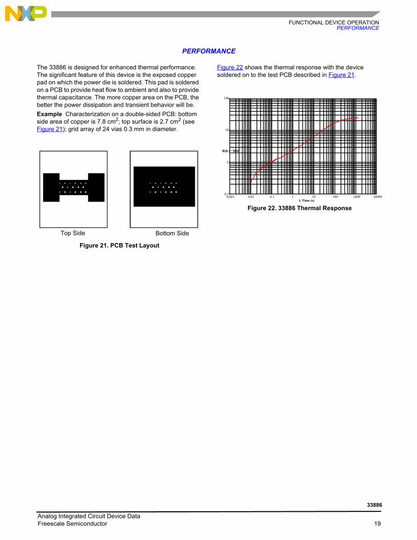
The 33886 is designed for enhanced thermal performance. The significant feature of this device is the exposed copper pad on which the power die is soldered. This pad is soldered on a PCB to provide heat flow to ambient and also to provide thermal capacitance. The more copper area on the PCB, the better the power dissipation and transient behavior will be.
Example Characterization on a double-sided PCB: bottom side area of copper is 7.8 cm2; top surface is 2.7 cm2 (see Figure 21); grid array of 24 vias 0.3 mm in diameter.
Figure 21. PCB Test Layout
Figure 22 shows the thermal response with the device soldered on to the test PCB described in Figure 21.
Figure 22. 33886 Thermal Response
Top Side Bottom Side
0,1
1
10
100
0,001 0,01 0,1 1 10 100 1000 10000t, Time (s)
Rth (¬¨ÐóC
Analog Integrated Circuit Device DataFreescale Semiconductor 19
33886
TYPICAL APPLICATIONS
TYPICAL APPLICATIONS
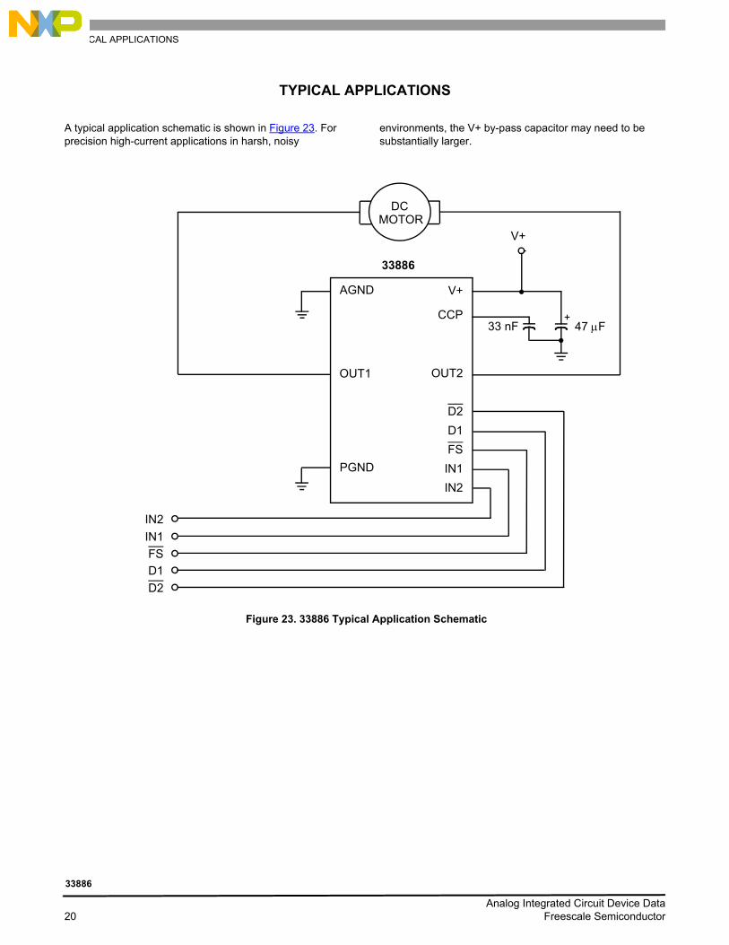
A typical application schematic is shown in Figure 23. For precision high-current applications in harsh, noisy
environments, the V+ by-pass capacitor may need to be substantially larger.
Figure 23. 33886 Typical Application Schematic
MOTOR
AGND
OUT1
PGND
V+
CCP
OUT2
D2
D1
FS
IN1
IN2
33 nF 47 F
V+
33886
+
IN2
IN1
FS
D1
D2
DC
Analog Integrated Circuit Device Data20 Freescale Semiconductor
33886
PACKAGINGPACKAGE DIMENSIONS
PACKAGING
PACKAGE DIMENSIONS
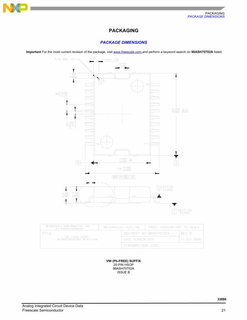
Important For the most current revision of the package, visit www.freescale.com and perform a keyword search on 98ASH70702A listed.
VW (Pb-FREE) SUFFIX20-PIN HSOP 98ASH70702A
ISSUE B
Analog Integrated Circuit Device DataFreescale Semiconductor 21
33886
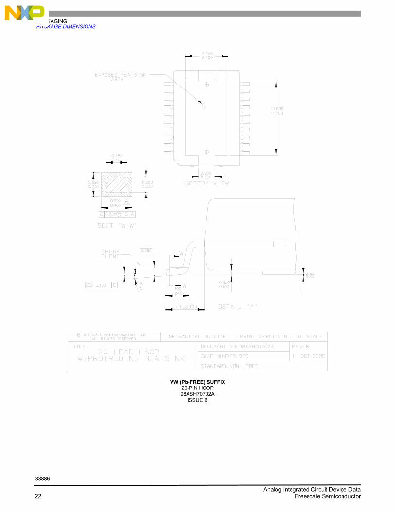
PACKAGINGPACKAGE DIMENSIONS
VW (Pb-FREE) SUFFIX20-PIN HSOP 98ASH70702A
ISSUE B
Analog Integrated Circuit Device Data22 Freescale Semiconductor
33886
PACKAGINGPACKAGE DIMENSIONS
VW (Pb-FREE) SUFFIX20-PIN HSOP 98ASH70702A
ISSUE B
Analog Integrated Circuit Device DataFreescale Semiconductor 23
33886
5.0 A H-BRIDGETHERMAL ADDENDUM - REVISION 2.0
5.0 A H-BRIDGE
THERMAL ADDENDUM - REVISION 2.0
Introduction
This thermal addendum is provided as a supplement to the MC33186 technical data sheet. The addendum provides thermal performance information that may be critical in the design and development of system applications. All electrical, application, and packaging information is provided in the data sheet.
Packaging and Thermal Considerations
The MC33186 is offered in a 20 pin HSOP exposed pad, single die package. There is a single heat source (P), a single junction temperature (TJ), and thermal resistance (RJA).
The stated values are solely for a thermal performance comparison of one package to another in a standardized environment. This methodology is not meant to and will not predict the performance of a package in an application-specific environment. Stated values were obtained by measurement and simulation according to the standards listed below.
Standards
NOTES:
1.Per JEDEC JESD51-2 at natural convection, still air condition.
2.2s2p thermal test board per JEDEC JESD51-5 and JESD51-7.
3.Per JEDEC JESD51-8, with the board temperature on the center trace near the center lead.
4.Single layer thermal test board per JEDEC JESD51-3 and JESD51-5.
5.Thermal resistance between the die junction and the exposed pad surface; cold plate attached to the package bottom side, remaining surfaces insulated.
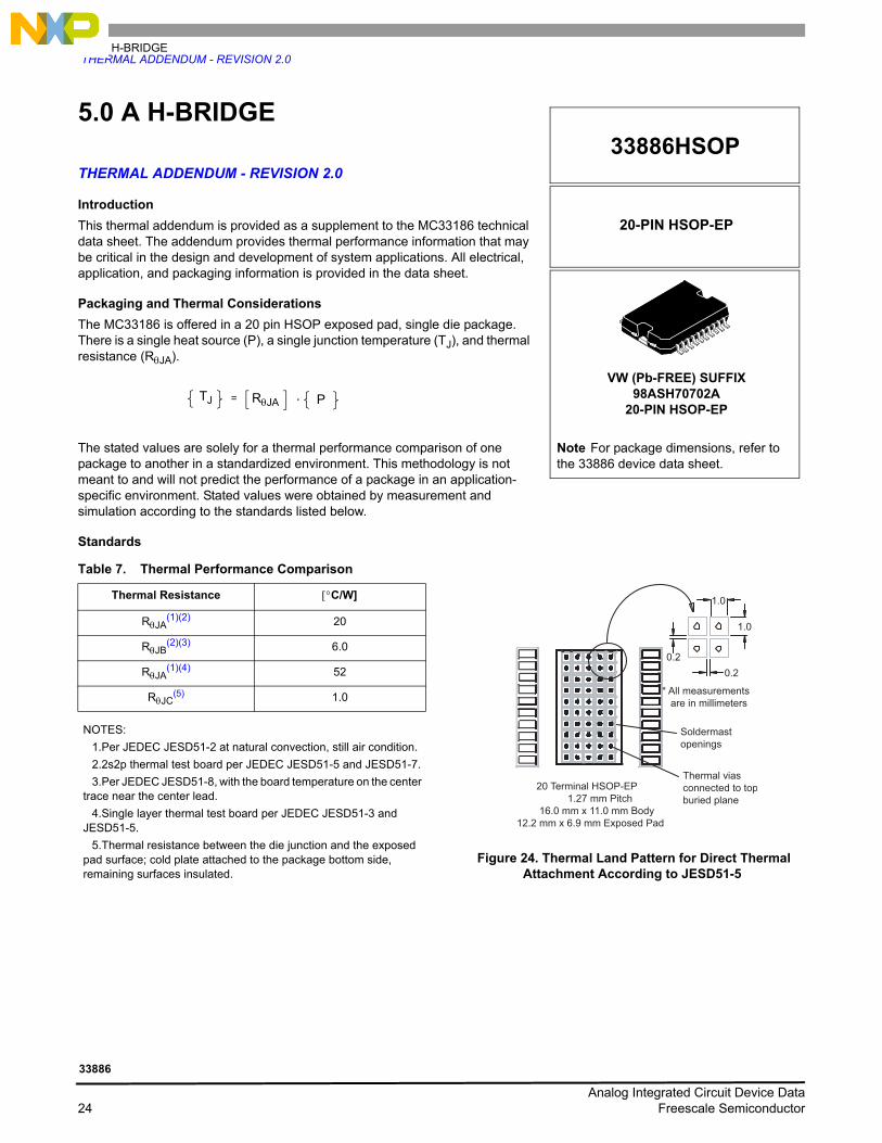
Figure 24. Thermal Land Pattern for Direct Thermal Attachment According to JESD51-5
20-PIN HSOP-EP
33886HSOP
Note For package dimensions, refer to the 33886 device data sheet.
VW (Pb-FREE) SUFFIX98ASH70702A
20-PIN HSOP-EPTJ = RJA . P
Table 7. Thermal Performance Comparison
Thermal Resistance C/W]
RJA(1)(2) 20
RJB(2)(3)
6.0
RJA(1)(4)
52
RJC(5)
1.0
1.0
1.0
0.2
0.2
Soldermast
openings
Thermal vias
connected to top
buried plane
* All measurements
are in millimeters
20 Terminal HSOP-EP
1.27 mm Pitch
16.0 mm x 11.0 mm Body
12.2 mm x 6.9 mm Exposed Pad
Analog Integrated Circuit Device Data24 Freescale Semiconductor
33886
5.0 A H-BRIDGETHERMAL ADDENDUM - REVISION 2.0
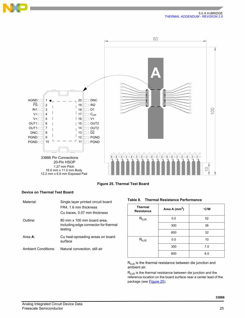
Figure 25. Thermal Test Board
Device on Thermal Test Board
RJAis the thermal resistance between die junction and ambient air.
RJS is the thermal resistance between die junction and the reference location on the board surface near a center lead of the package (see Figure 25).
20-Pin HSOP1.27 mm Pitch
16.0 mm x 11.0 mm Body12.2 mm x 6.9 mm Exposed Pad
DNCAGND
IN2
D1
CCP
V+
OUT2
OUT2
D2
PGND
PGND
FS
V+
OUT1
OUT1
DNC
PGND
PGND
IN1
V+
1
2
34
5
67
8
910
20
19
16
1514
13
1211
1817
33886 Pin Connections
A
Material: Single layer printed circuit board
FR4, 1.6 mm thickness
Cu traces, 0.07 mm thickness
Outline: 80 mm x 100 mm board area, including edge connector for thermal testing
Area A: Cu heat-spreading areas on board surface
Ambient Conditions: Natural convection, still air
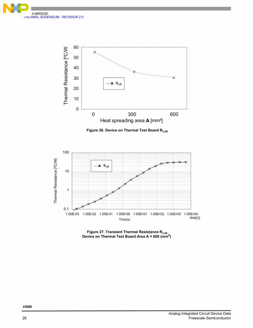
Table 8. Thermal Resistance Performance
Thermal Resistance
Area A (mm2) C/W
RJA 0.0 52
300 36
600 32
RJS 0.0 10
300 7.0
600 6.0
Analog Integrated Circuit Device DataFreescale Semiconductor 25
33886
5.0 A H-BRIDGETHERMAL ADDENDUM - REVISION 2.0
Figure 26. Device on Thermal Test Board RJA
Figure 27. Transient Thermal Resistance RJADevice on Thermal Test Board Area A = 600 (mm2)
0
10
20
30
40
50
60
Heat spreading area A [mm²]
Th
erm
al R
esi
sta
nce
[ºC
/W]
0 300 600
x RJA
0.1
1
10
100
1.00E-03 1.00E-02 1.00E-01 1.00E+00 1.00E+01 1.00E+02 1.00E+03 1.00E+04time[s]
Th
erm
al R
esi
sta
nce
[ºC
/W]
Time(s)
x RJA
Analog Integrated Circuit Device Data26 Freescale Semiconductor
33886
Analog Integrated Circuit Device DataFreescale Semiconductor 27
33886
REVISION HISTORY
REVISION HISTORY
Revision Date Description of Changes
7.0 7/2005• Implemented Revision History page• Added Thermal Addendum• Converted to Freescale format
8.0 2/2007
• Updated data sheet format• Removed Peak Package Reflow Temperature During Reflow (solder reflow) parameter from
Maximum Ratings on page 5. Added note with instructions to obtain this information from www.freescale.com.
9.0 3/2011
• Removed part number MC33886VW/R2 and added part number MC33886PVW/R2 to the ordering Information on page 1.
• Updated package drawing.• Removed all DH package information.• Updated form and style
10.0 01/2014• No technical changes. Revised back page. Updated document properties. Added SMARTMOS
sentence to last paragraph.

Document Number: MC33886Rev 10.001/2014
Information in this document is provided solely to enable system and software implementers to use Freescale products.
There are no express or implied copyright licenses granted hereunder to design or fabricate any integrated circuits based
on the information in this document.
Freescale reserves the right to make changes without further notice to any products herein. Freescale makes no
warranty, representation, or guarantee regarding the suitability of its products for any particular purpose, nor does
Freescale assume any liability arising out of the application or use of any product or circuit, and specifically disclaims any
and all liability, including without limitation consequential or incidental damages. “Typical” parameters that may be
provided in Freescale data sheets and/or specifications can and do vary in different applications, and actual performance
may vary over time. All operating parameters, including “typicals,” must be validated for each customer application by
customer’s technical experts. Freescale does not convey any license under its patent rights nor the rights of others.
Freescale sells products pursuant to standard terms and conditions of sale, which can be found at the following address:
freescale.com/SalesTermsandConditions.
Freescale and the Freescale logo are trademarks of Freescale Semiconductor, Inc., Reg. U.S. Pat. & Tm. Off.
SMARTMOS is a trademark of Freescale Semiconductor, Inc. All other product or service names are the property of their
respective owners.
© 2014 Freescale Semiconductor, Inc.
How to Reach Us:
Home Page: freescale.com
Web Support: freescale.com/support